WO2010023720A1 - 構造体、電子装置及び構造体の形成方法 - Google Patents
構造体、電子装置及び構造体の形成方法 Download PDFInfo
- Publication number
- WO2010023720A1 WO2010023720A1 PCT/JP2008/065128 JP2008065128W WO2010023720A1 WO 2010023720 A1 WO2010023720 A1 WO 2010023720A1 JP 2008065128 W JP2008065128 W JP 2008065128W WO 2010023720 A1 WO2010023720 A1 WO 2010023720A1
- Authority
- WO
- WIPO (PCT)
- Prior art keywords
- cnt bundle
- carbon nanotubes
- cnt
- bundle
- conductive film
- Prior art date
- Legal status (The legal status is an assumption and is not a legal conclusion. Google has not performed a legal analysis and makes no representation as to the accuracy of the status listed.)
- Ceased
Links
Images







Classifications
-
- H—ELECTRICITY
- H01—ELECTRIC ELEMENTS
- H01H—ELECTRIC SWITCHES; RELAYS; SELECTORS; EMERGENCY PROTECTIVE DEVICES
- H01H1/00—Contacts
- H01H1/0036—Switches making use of microelectromechanical systems [MEMS]
-
- B—PERFORMING OPERATIONS; TRANSPORTING
- B81—MICROSTRUCTURAL TECHNOLOGY
- B81C—PROCESSES OR APPARATUS SPECIALLY ADAPTED FOR THE MANUFACTURE OR TREATMENT OF MICROSTRUCTURAL DEVICES OR SYSTEMS
- B81C1/00—Manufacture or treatment of devices or systems in or on a substrate
- B81C1/00015—Manufacture or treatment of devices or systems in or on a substrate for manufacturing microsystems
- B81C1/00134—Manufacture or treatment of devices or systems in or on a substrate for manufacturing microsystems comprising flexible or deformable structures
- B81C1/00166—Electrodes
-
- B—PERFORMING OPERATIONS; TRANSPORTING
- B82—NANOTECHNOLOGY
- B82Y—SPECIFIC USES OR APPLICATIONS OF NANOSTRUCTURES; MEASUREMENT OR ANALYSIS OF NANOSTRUCTURES; MANUFACTURE OR TREATMENT OF NANOSTRUCTURES
- B82Y10/00—Nanotechnology for information processing, storage or transmission, e.g. quantum computing or single electron logic
-
- B—PERFORMING OPERATIONS; TRANSPORTING
- B82—NANOTECHNOLOGY
- B82Y—SPECIFIC USES OR APPLICATIONS OF NANOSTRUCTURES; MEASUREMENT OR ANALYSIS OF NANOSTRUCTURES; MANUFACTURE OR TREATMENT OF NANOSTRUCTURES
- B82Y30/00—Nanotechnology for materials or surface science, e.g. nanocomposites
-
- B—PERFORMING OPERATIONS; TRANSPORTING
- B82—NANOTECHNOLOGY
- B82Y—SPECIFIC USES OR APPLICATIONS OF NANOSTRUCTURES; MEASUREMENT OR ANALYSIS OF NANOSTRUCTURES; MANUFACTURE OR TREATMENT OF NANOSTRUCTURES
- B82Y40/00—Manufacture or treatment of nanostructures
-
- C—CHEMISTRY; METALLURGY
- C01—INORGANIC CHEMISTRY
- C01B—NON-METALLIC ELEMENTS; COMPOUNDS THEREOF; METALLOIDS OR COMPOUNDS THEREOF NOT COVERED BY SUBCLASS C01C
- C01B32/00—Carbon; Compounds thereof
- C01B32/15—Nano-sized carbon materials
- C01B32/158—Carbon nanotubes
- C01B32/16—Preparation
-
- D—TEXTILES; PAPER
- D01—NATURAL OR MAN-MADE THREADS OR FIBRES; SPINNING
- D01F—CHEMICAL FEATURES IN THE MANUFACTURE OF ARTIFICIAL FILAMENTS, THREADS, FIBRES, BRISTLES OR RIBBONS; APPARATUS SPECIALLY ADAPTED FOR THE MANUFACTURE OF CARBON FILAMENTS
- D01F9/00—Artificial filaments or the like of other substances; Manufacture thereof; Apparatus specially adapted for the manufacture of carbon filaments
- D01F9/08—Artificial filaments or the like of other substances; Manufacture thereof; Apparatus specially adapted for the manufacture of carbon filaments of inorganic material
- D01F9/12—Carbon filaments; Apparatus specially adapted for the manufacture thereof
- D01F9/127—Carbon filaments; Apparatus specially adapted for the manufacture thereof by thermal decomposition of hydrocarbon gases or vapours or other carbon-containing compounds in the form of gas or vapour, e.g. carbon monoxide, alcohols
-
- D—TEXTILES; PAPER
- D01—NATURAL OR MAN-MADE THREADS OR FIBRES; SPINNING
- D01F—CHEMICAL FEATURES IN THE MANUFACTURE OF ARTIFICIAL FILAMENTS, THREADS, FIBRES, BRISTLES OR RIBBONS; APPARATUS SPECIALLY ADAPTED FOR THE MANUFACTURE OF CARBON FILAMENTS
- D01F9/00—Artificial filaments or the like of other substances; Manufacture thereof; Apparatus specially adapted for the manufacture of carbon filaments
- D01F9/08—Artificial filaments or the like of other substances; Manufacture thereof; Apparatus specially adapted for the manufacture of carbon filaments of inorganic material
- D01F9/12—Carbon filaments; Apparatus specially adapted for the manufacture thereof
- D01F9/127—Carbon filaments; Apparatus specially adapted for the manufacture thereof by thermal decomposition of hydrocarbon gases or vapours or other carbon-containing compounds in the form of gas or vapour, e.g. carbon monoxide, alcohols
- D01F9/133—Apparatus therefor
-
- B—PERFORMING OPERATIONS; TRANSPORTING
- B81—MICROSTRUCTURAL TECHNOLOGY
- B81B—MICROSTRUCTURAL DEVICES OR SYSTEMS, e.g. MICROMECHANICAL DEVICES
- B81B2207/00—Microstructural systems or auxiliary parts thereof
- B81B2207/07—Interconnects
-
- H—ELECTRICITY
- H01—ELECTRIC ELEMENTS
- H01H—ELECTRIC SWITCHES; RELAYS; SELECTORS; EMERGENCY PROTECTIVE DEVICES
- H01H1/00—Contacts
- H01H1/02—Contacts characterised by the material thereof
- H01H1/021—Composite material
- H01H1/027—Composite material containing carbon particles or fibres
-
- H—ELECTRICITY
- H01—ELECTRIC ELEMENTS
- H01H—ELECTRIC SWITCHES; RELAYS; SELECTORS; EMERGENCY PROTECTIVE DEVICES
- H01H1/00—Contacts
- H01H1/0036—Switches making use of microelectromechanical systems [MEMS]
- H01H2001/0052—Special contact materials used for MEMS
-
- H—ELECTRICITY
- H01—ELECTRIC ELEMENTS
- H01H—ELECTRIC SWITCHES; RELAYS; SELECTORS; EMERGENCY PROTECTIVE DEVICES
- H01H2300/00—Orthogonal indexing scheme relating to electric switches, relays, selectors or emergency protective devices covered by H01H
- H01H2300/036—Application nanoparticles, e.g. nanotubes, integrated in switch components, e.g. contacts, the switch itself being clearly of a different scale, e.g. greater than nanoscale
-
- H—ELECTRICITY
- H10—SEMICONDUCTOR DEVICES; ELECTRIC SOLID-STATE DEVICES NOT OTHERWISE PROVIDED FOR
- H10W—GENERIC PACKAGES, INTERCONNECTIONS, CONNECTORS OR OTHER CONSTRUCTIONAL DETAILS OF DEVICES COVERED BY CLASS H10
- H10W72/00—Interconnections or connectors in packages
- H10W72/01—Manufacture or treatment
- H10W72/011—Apparatus therefor
- H10W72/0112—Apparatus for manufacturing bump connectors
-
- H—ELECTRICITY
- H10—SEMICONDUCTOR DEVICES; ELECTRIC SOLID-STATE DEVICES NOT OTHERWISE PROVIDED FOR
- H10W—GENERIC PACKAGES, INTERCONNECTIONS, CONNECTORS OR OTHER CONSTRUCTIONAL DETAILS OF DEVICES COVERED BY CLASS H10
- H10W72/00—Interconnections or connectors in packages
- H10W72/01—Manufacture or treatment
- H10W72/012—Manufacture or treatment of bump connectors, dummy bumps or thermal bumps
- H10W72/01215—Manufacture or treatment of bump connectors, dummy bumps or thermal bumps forming coatings
-
- H—ELECTRICITY
- H10—SEMICONDUCTOR DEVICES; ELECTRIC SOLID-STATE DEVICES NOT OTHERWISE PROVIDED FOR
- H10W—GENERIC PACKAGES, INTERCONNECTIONS, CONNECTORS OR OTHER CONSTRUCTIONAL DETAILS OF DEVICES COVERED BY CLASS H10
- H10W72/00—Interconnections or connectors in packages
- H10W72/01—Manufacture or treatment
- H10W72/012—Manufacture or treatment of bump connectors, dummy bumps or thermal bumps
- H10W72/01231—Manufacture or treatment of bump connectors, dummy bumps or thermal bumps using blanket deposition
- H10W72/01238—Manufacture or treatment of bump connectors, dummy bumps or thermal bumps using blanket deposition in gaseous form, e.g. by CVD or PVD
-
- H—ELECTRICITY
- H10—SEMICONDUCTOR DEVICES; ELECTRIC SOLID-STATE DEVICES NOT OTHERWISE PROVIDED FOR
- H10W—GENERIC PACKAGES, INTERCONNECTIONS, CONNECTORS OR OTHER CONSTRUCTIONAL DETAILS OF DEVICES COVERED BY CLASS H10
- H10W72/00—Interconnections or connectors in packages
- H10W72/01—Manufacture or treatment
- H10W72/012—Manufacture or treatment of bump connectors, dummy bumps or thermal bumps
- H10W72/01251—Changing the shapes of bumps
- H10W72/01255—Changing the shapes of bumps by using masks
-
- H—ELECTRICITY
- H10—SEMICONDUCTOR DEVICES; ELECTRIC SOLID-STATE DEVICES NOT OTHERWISE PROVIDED FOR
- H10W—GENERIC PACKAGES, INTERCONNECTIONS, CONNECTORS OR OTHER CONSTRUCTIONAL DETAILS OF DEVICES COVERED BY CLASS H10
- H10W72/00—Interconnections or connectors in packages
- H10W72/071—Connecting or disconnecting
- H10W72/072—Connecting or disconnecting of bump connectors
-
- H—ELECTRICITY
- H10—SEMICONDUCTOR DEVICES; ELECTRIC SOLID-STATE DEVICES NOT OTHERWISE PROVIDED FOR
- H10W—GENERIC PACKAGES, INTERCONNECTIONS, CONNECTORS OR OTHER CONSTRUCTIONAL DETAILS OF DEVICES COVERED BY CLASS H10
- H10W72/00—Interconnections or connectors in packages
- H10W72/071—Connecting or disconnecting
- H10W72/072—Connecting or disconnecting of bump connectors
- H10W72/07221—Aligning
- H10W72/07227—Aligning involving guiding structures, e.g. spacers or supporting members
-
- H—ELECTRICITY
- H10—SEMICONDUCTOR DEVICES; ELECTRIC SOLID-STATE DEVICES NOT OTHERWISE PROVIDED FOR
- H10W—GENERIC PACKAGES, INTERCONNECTIONS, CONNECTORS OR OTHER CONSTRUCTIONAL DETAILS OF DEVICES COVERED BY CLASS H10
- H10W72/00—Interconnections or connectors in packages
- H10W72/20—Bump connectors, e.g. solder bumps or copper pillars; Dummy bumps; Thermal bumps
- H10W72/241—Dispositions, e.g. layouts
-
- H—ELECTRICITY
- H10—SEMICONDUCTOR DEVICES; ELECTRIC SOLID-STATE DEVICES NOT OTHERWISE PROVIDED FOR
- H10W—GENERIC PACKAGES, INTERCONNECTIONS, CONNECTORS OR OTHER CONSTRUCTIONAL DETAILS OF DEVICES COVERED BY CLASS H10
- H10W72/00—Interconnections or connectors in packages
- H10W72/20—Bump connectors, e.g. solder bumps or copper pillars; Dummy bumps; Thermal bumps
- H10W72/241—Dispositions, e.g. layouts
- H10W72/242—Dispositions, e.g. layouts relative to the surface, e.g. recessed, protruding
-
- H—ELECTRICITY
- H10—SEMICONDUCTOR DEVICES; ELECTRIC SOLID-STATE DEVICES NOT OTHERWISE PROVIDED FOR
- H10W—GENERIC PACKAGES, INTERCONNECTIONS, CONNECTORS OR OTHER CONSTRUCTIONAL DETAILS OF DEVICES COVERED BY CLASS H10
- H10W72/00—Interconnections or connectors in packages
- H10W72/20—Bump connectors, e.g. solder bumps or copper pillars; Dummy bumps; Thermal bumps
- H10W72/241—Dispositions, e.g. layouts
- H10W72/245—Dispositions, e.g. layouts of outermost layers of multilayered bumps, e.g. bump coating being only on a part of a bump core
-
- H—ELECTRICITY
- H10—SEMICONDUCTOR DEVICES; ELECTRIC SOLID-STATE DEVICES NOT OTHERWISE PROVIDED FOR
- H10W—GENERIC PACKAGES, INTERCONNECTIONS, CONNECTORS OR OTHER CONSTRUCTIONAL DETAILS OF DEVICES COVERED BY CLASS H10
- H10W72/00—Interconnections or connectors in packages
- H10W72/20—Bump connectors, e.g. solder bumps or copper pillars; Dummy bumps; Thermal bumps
- H10W72/251—Materials
- H10W72/253—Materials not comprising solid metals or solid metalloids, e.g. polymers or ceramics
-
- H—ELECTRICITY
- H10—SEMICONDUCTOR DEVICES; ELECTRIC SOLID-STATE DEVICES NOT OTHERWISE PROVIDED FOR
- H10W—GENERIC PACKAGES, INTERCONNECTIONS, CONNECTORS OR OTHER CONSTRUCTIONAL DETAILS OF DEVICES COVERED BY CLASS H10
- H10W72/00—Interconnections or connectors in packages
- H10W72/20—Bump connectors, e.g. solder bumps or copper pillars; Dummy bumps; Thermal bumps
- H10W72/251—Materials
- H10W72/255—Materials of outermost layers of multilayered bumps, e.g. material of a coating
-
- H—ELECTRICITY
- H10—SEMICONDUCTOR DEVICES; ELECTRIC SOLID-STATE DEVICES NOT OTHERWISE PROVIDED FOR
- H10W—GENERIC PACKAGES, INTERCONNECTIONS, CONNECTORS OR OTHER CONSTRUCTIONAL DETAILS OF DEVICES COVERED BY CLASS H10
- H10W72/00—Interconnections or connectors in packages
- H10W72/20—Bump connectors, e.g. solder bumps or copper pillars; Dummy bumps; Thermal bumps
- H10W72/29—Bond pads specially adapted therefor
-
- H—ELECTRICITY
- H10—SEMICONDUCTOR DEVICES; ELECTRIC SOLID-STATE DEVICES NOT OTHERWISE PROVIDED FOR
- H10W—GENERIC PACKAGES, INTERCONNECTIONS, CONNECTORS OR OTHER CONSTRUCTIONAL DETAILS OF DEVICES COVERED BY CLASS H10
- H10W72/00—Interconnections or connectors in packages
- H10W72/90—Bond pads, in general
- H10W72/921—Structures or relative sizes of bond pads
- H10W72/923—Bond pads having multiple stacked layers
-
- H—ELECTRICITY
- H10—SEMICONDUCTOR DEVICES; ELECTRIC SOLID-STATE DEVICES NOT OTHERWISE PROVIDED FOR
- H10W—GENERIC PACKAGES, INTERCONNECTIONS, CONNECTORS OR OTHER CONSTRUCTIONAL DETAILS OF DEVICES COVERED BY CLASS H10
- H10W72/00—Interconnections or connectors in packages
- H10W72/90—Bond pads, in general
- H10W72/941—Dispositions of bond pads
- H10W72/9415—Dispositions of bond pads relative to the surface, e.g. recessed, protruding
-
- H—ELECTRICITY
- H10—SEMICONDUCTOR DEVICES; ELECTRIC SOLID-STATE DEVICES NOT OTHERWISE PROVIDED FOR
- H10W—GENERIC PACKAGES, INTERCONNECTIONS, CONNECTORS OR OTHER CONSTRUCTIONAL DETAILS OF DEVICES COVERED BY CLASS H10
- H10W72/00—Interconnections or connectors in packages
- H10W72/90—Bond pads, in general
- H10W72/941—Dispositions of bond pads
- H10W72/942—Dispositions of bond pads relative to underlying supporting features, e.g. bond pads, RDLs or vias
-
- H—ELECTRICITY
- H10—SEMICONDUCTOR DEVICES; ELECTRIC SOLID-STATE DEVICES NOT OTHERWISE PROVIDED FOR
- H10W—GENERIC PACKAGES, INTERCONNECTIONS, CONNECTORS OR OTHER CONSTRUCTIONAL DETAILS OF DEVICES COVERED BY CLASS H10
- H10W90/00—Package configurations
- H10W90/701—Package configurations characterised by the relative positions of pads or connectors relative to package parts
- H10W90/721—Package configurations characterised by the relative positions of pads or connectors relative to package parts of bump connectors
- H10W90/724—Package configurations characterised by the relative positions of pads or connectors relative to package parts of bump connectors between a chip and a stacked insulating package substrate, interposer or RDL
-
- Y—GENERAL TAGGING OF NEW TECHNOLOGICAL DEVELOPMENTS; GENERAL TAGGING OF CROSS-SECTIONAL TECHNOLOGIES SPANNING OVER SEVERAL SECTIONS OF THE IPC; TECHNICAL SUBJECTS COVERED BY FORMER USPC CROSS-REFERENCE ART COLLECTIONS [XRACs] AND DIGESTS
- Y10—TECHNICAL SUBJECTS COVERED BY FORMER USPC
- Y10T—TECHNICAL SUBJECTS COVERED BY FORMER US CLASSIFICATION
- Y10T428/00—Stock material or miscellaneous articles
- Y10T428/23907—Pile or nap type surface or component
- Y10T428/23943—Flock surface
-
- Y—GENERAL TAGGING OF NEW TECHNOLOGICAL DEVELOPMENTS; GENERAL TAGGING OF CROSS-SECTIONAL TECHNOLOGIES SPANNING OVER SEVERAL SECTIONS OF THE IPC; TECHNICAL SUBJECTS COVERED BY FORMER USPC CROSS-REFERENCE ART COLLECTIONS [XRACs] AND DIGESTS
- Y10—TECHNICAL SUBJECTS COVERED BY FORMER USPC
- Y10T—TECHNICAL SUBJECTS COVERED BY FORMER US CLASSIFICATION
- Y10T428/00—Stock material or miscellaneous articles
- Y10T428/31504—Composite [nonstructural laminate]
- Y10T428/31678—Of metal
Definitions
- the present invention relates to a structure using a carbon nanotube, an electronic device, and a method for forming the structure.
- Carbon nanotubes (hereinafter referred to as CNT) have high electrical conduction characteristics, thermal conduction characteristics, and mechanical strength, and are attracting attention as materials for wiring, electrodes, contacts, and the like instead of metals.
- CNT bundles such as pads and bumps of semiconductor devices as bundles of many bundles (hereinafter referred to as CNT bundles).
- Proposals have been made (see, for example, Patent Document 1 and Non-Patent Document 1).
- Patent Document 1 and Non-Patent Document 1 when used as a wider range of connection terminals and electrodes, there are the following problems.
- An object of the present invention is to provide a structure, an electronic device, and a method for forming a structure that can prevent CNTs from being scattered.
- a conductive film provided on the underlayer and a CNT bundle composed of a plurality of carbon nanotubes, one end of which is connected to the conductive film Among the carbon nanotubes, at least the carbon nanotubes on the outer side of the CNT bundle are stretched with a convex curvature toward the outside of the CNT bundle, and the curvature increases toward the outer periphery of the CNT bundle, and toward the other end.
- a structure with a reduced diameter is provided.
- the first CNT bundle is composed of a plurality of first carbon nanotubes whose one ends are connected to the first wiring provided in the underlayer, and a plurality of the first CNT bundles are arranged on the other end side.
- the first carbon nanotubes at least the carbon nanotubes on the outer side of the first CNT bundle extend with a convex curvature toward the outside of the CNT bundle, and the curvature increases toward the outer periphery of the first CNT bundle.
- An electronic device is provided.
- a structure forming method for growing a CNT bundle composed of a plurality of carbon nanotubes connected at one end to a conductive film formed on an underlayer in a reaction chamber in which plasma is generated. And, at the other end of the CNT bundle, at least the carbon nanotubes on the outer side of the CNT bundle grow with a convex curvature toward the outside of the CNT bundle, and toward the outer periphery of the CNT bundle.
- the growth temperature, the concentration of hydrocarbon gas supplied to the reaction chamber, and the grid potential of the grid provided between the plasma and the conductive film are set so that the curvature increases and the diameter of the CNT bundle decreases toward the other end.
- a method of forming a structure is provided.
- the present invention it is possible to provide a structure, an electronic device, and a structure forming method that can prevent the CNT bundle from being scattered.
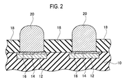
- FIG. 2 is a schematic view showing a II-II cross section of the structure shown in FIG. It is the schematic which shows an example of the apparatus used for the growth of CNT which concerns on embodiment of this invention.
- It is a schematic sectional drawing (the 1) which shows an example of the formation method of the CNT bundle which concerns on embodiment of this invention.
- It is a schematic sectional drawing (the 2) which shows an example of the formation method of the CNT bundle which concerns on embodiment of this invention.
- FIG. 23 is a schematic view showing a section XXIII-XXIII of the probe shown in FIG.
- FIG. 23 is a schematic view showing a section XXIII-XXIII of the probe shown in FIG.
- FIG. 23 is a schematic view showing a section XXIII-XXIII of the probe shown in FIG.
- FIG. 23 is a schematic view showing a section XXIII-XXIII of the probe shown in FIG.
- FIG. 23 is a cross-sectional schematic diagram which shows the other example of the probe using the structure which concerns on the 2nd application example of embodiment of this invention.
- the structure according to the embodiment of the present invention includes a plurality of conductive films (12, 14) provided in the base layer 10, and a plurality of conductive films (12 , 14) connected to each of a plurality of CNT bundles (hereinafter referred to as “CNT bundles”) 20.
- the plurality of CNT bundles 20 are respectively disposed in through holes provided in the insulating film 18 on the base layer 10.
- a catalyst layer 16 is disposed between each conductive film (12, 14) and the CNT bundle 20.
- Each conductive film (12, 14) is composed of a first conductive film 12 and a second conductive film 14, respectively.
- the CNT bundle 20 is used as a contact electrode such as a bump of an electronic device such as a semiconductor device.
- the conductive films (12, 14) are used as wirings connected to a semiconductor circuit or the like formed on the semiconductor substrate.
- the underlayer 10 is a wiring layer provided on the semiconductor substrate.
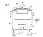
- FIG. 3 shows a surface wave plasma CVD apparatus as an example.
- the microwave introduced from the microwave waveguide 60 is introduced into the reaction chamber 6 from the slit antenna 62 through the quartz window 63.
- Plasma is generated by discharging in the reaction chamber 6 by the introduced microwave.
- An ion trap 64 made of quartz glass or the like is provided for reducing the ion component by retaining plasma in the discharge region 76 in the reaction chamber 6 near the slit antenna 62.
- a source gas is introduced into the reaction chamber 6 from a gas inlet 70.
- the reaction chamber 6 is evacuated by a vacuum pump 72 and maintained at a predetermined pressure by a flow rate of the raw material gas and an automatic pressure regulator (APC) 74.
- the substrate 2 is placed on the heater built-in susceptor 68 and maintained at a predetermined growth temperature.
- a grid 66 is disposed between the discharge region 76 and the substrate 2.
- a grid potential is applied to the grid 66 by a power source 67 so as to suppress a charge component diffused from the discharge region 76 onto the substrate 2.
- hydrocarbon gases such as methane (CH 4 ) and acetylene (C 2 H 2 ), and dilution gases such as hydrogen (H 2 ), argon (Ar), helium (He), and nitrogen (N 2 ) Is used.
- dilution gases such as hydrogen (H 2 ), argon (Ar), helium (He), and nitrogen (N 2 ) Is used.
- hydrogen H 2
- argon Ar
- He helium
- N 2 nitrogen
- first and second conductive films 12 and 14 are provided on the base layer 10 on the substrate 2.
- An insulating film 18 is formed on the base layer 10, and a through hole is provided in the insulating film 18 so that the surface of the second conductive film 14 is exposed.
- the catalyst metal is evaporated by physical vapor deposition such as laser ablation to form the catalyst layer 16 on the surface of the second conductive film 14.
- the substrate 2 thus prepared is placed on the susceptor 68 of the plasma CVD apparatus shown in FIG. 3, and CNT growth is performed.
- CH 4 gas and H 2 gas are used as source gas, and the concentration of CH 4 gas is set to about 10%.
- the grid potential is grounded.
- the growth temperature is about 600 ° C. to about 900 ° C., desirably about 600 ° C. to about 700 ° C.
- the first region 24a of the CNT bundle 20 composed of a plurality of CNTs 22 connected at one end to the catalyst layer 16 on the second conductive film 14 grows.
- Each of the grown CNTs 22 converges toward the center of the CNT bundle 20 by van der Waals force. Therefore, at least the CNTs 22 on the outer side of the CNT bundle 20 out of the plurality of CNTs 22 grow to have a convex curvature toward the outside, and the curvature increases toward the outer periphery of the CNT bundle 20. Therefore, the diameter of the CNT bundle 20 decreases toward the tip of the CNT bundle 20. Further, since the source gas is sufficiently supplied to the outer peripheral portion of the CNT bundle 20, the length of each of the plurality of CNTs 22 increases from the inside to the outside of the CNT bundle 20.
- the growth temperature is lowered to about 400 ° C. to about 600 ° C., desirably about 400 ° C. to about 500 ° C.
- the growth of the CNT 22 occurs at the interface with the catalyst layer 16, and the second region 24b grows below the first region 24a. Since the growth temperature is lowered, CNTs 22 having low linearity and meandering grow. As a result, the plurality of CNTs 22 are suppressed from converging to the central portion by van der Waals force, and the outer diameter of the second region 24b can be kept substantially constant. In this way, the CNT bundle 20 having the first and second regions 24a and 24b is formed.
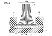
- FIG. 6 shows, as a comparative example, a CNT bundle 20a when the CNTs 22 are grown without lowering the growth temperature.
- the plurality of CNTs 22 grow with good linearity.
- the CNT 22 grows so as to extend with a concave curvature toward the outer periphery at the base end portion, and a substantially linear CNT bundle 20a having a smaller diameter than the base end portion is obtained at the tip end portion.
- the CNT bundle 20a of the comparative example since the CNTs 22 are substantially straight at the tip, if the pressure is applied from the tip of the CNT bundle 20a, the CNT bundle 20a is scattered.
- the distal end portion of the CNT bundle 20 has a convex curvature toward the outer periphery of the CNT bundle 20, and has an envelope shape in which a plurality of CNTs 22 converge toward the center. Take. Therefore, it is difficult for the CNT bundle 20 itself to be scattered.
- the catalyst layer 16 acts as a catalyst metal for the growth of the CNT bundle 20.
- metal particles such as a metal such as cobalt (Co), nickel (Ni), iron (Fe), or an alloy mainly composed of Co, Ni, Fe, or the like are used.
- the CNT diameter of the CNT bundle 20 is controlled by the diameter of the catalyst layer 16. Therefore, the average particle diameter of the catalyst layer 16 is in the range of about 2 nm to about 10 nm, desirably about 4 nm to about 6 nm.
- the average particle diameter is an average diameter when the metal particles are regarded as spherical, and is measured by, for example, a laser diffraction scattering method.
- the first conductive film 12 is made of a metal such as copper (Cu), aluminum (Al), or tungsten (W).
- TiN titanium nitride
- As a material for the low dielectric constant insulating film an inorganic material such as carbon-added silicon oxide (SiOC) or inorganic spin-on-glass (SOG), or an organic material such as organic SOG can be used.
- a laminated film such as an inorganic material film and an organic material film may be used as the low dielectric constant insulating film.
- the structure according to the embodiment of the present invention is provided on the uppermost wiring (first wiring) of the first substrate on which the semiconductor circuit is formed, and used as a contact electrode such as a bump.
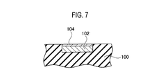
- a conductive film 102 such as Cu and a conductive film 104 such as TiN are formed over the conductive film 102 as the second wiring on the second substrate 100 used as a mounting substrate such as a package.
- the conductive film 104 of the second wiring is opposed to and electrically connected to the CNT bundle 20 that is a contact electrode.
- the CNT bundle 20 is pressed and connected to the second wiring. Since the CNT bundle 20 is convex toward the outer periphery, it is possible to prevent the CNT bundle 20 from being opened outward or buckled even if pressure is applied. In addition, since the CNT bundle 20 is not scattered even when pressure is applied, there is no possibility of contact with an adjacent structure, and the pitch of the contact electrodes can be reduced.
- the CNT 22 has a structure having higher meandering property than the tip end portion. Therefore, contact with higher pressure is possible. Further, as shown in FIG. 5, since the plurality of CNTs 22 meander, reliable connection is possible due to the spring effect.
- the first and second regions 24a and 24b of the CNT bundle 20 are grown by changing the growth temperature.
- the first and second regions 24a and 24b can be grown by changing at least one of the growth temperature, the concentration of hydrocarbon gas, or the grid potential.
- the growth temperature is about 600 ° C. and the grid potential is grounded.
- the first region 24a can be grown by setting the CH 4 gas concentration as low as about 1% to about 0.01%, desirably about 1% to about 0.1%.
- the second region 24b can be grown by increasing the CH 4 gas concentration to about 10% to about 100%, desirably about 10% to about 50%.
- the growth temperature is about 600 ° C. and the CH 4 gas concentration is about 10%.
- the first region 24a can be grown by setting the grid potential to a positive potential.
- the second region 24b can be grown by lowering the grid potential or making it floating.
- a first conductive film 12 such as Cu and TiN are formed on a wiring layer (underlayer) 10 formed on a substrate on which a semiconductor circuit or the like is formed by photolithography, etching, sputtering, or the like.
- a second conductive film 14 is formed. The first and second conductive films 12 and 14 are used as wiring.
- an insulating film 18 such as SiO 2 is formed on the wiring layer 10 by CVD or the like.
- a part of the insulating film 18 is selectively removed by photolithography, etching or the like to form a through hole 30.
- the surface of the second conductive film 14 is exposed in the through hole 30.
- a catalyst layer 16 such as Co is formed on the surface of the second conductive film 14 exposed in the through hole 30 by physical vapor deposition or the like.
- a CNT bundle 20 is grown on the catalyst layer 16 by plasma CVD using the plasma CVD apparatus shown in FIG. First, CNT growth is performed at a growth temperature of about 600 ° C., a CH 4 concentration of about 10%, and a grid potential at ground. Thereafter, the growth temperature is lowered to about 500 ° C. to perform CNT growth. As a result, a CNT bundle 20 having a convex curvature toward the outer periphery at the distal end and a shape that embeds the through hole 30 at the proximal end is formed.
- a remote plasma is generated inside the reaction chamber 6 by a surface wave type electromagnetic wave introduction method. Therefore, generation of amorphous carbon or the like and plasma damage to the catalyst layer 16 are minimized.
- the ion component contained in the discharge active species excited by the microwave power introduced from the surface wave type slit antenna 62 may generate amorphous carbon during CNT growth.
- the ion trap 64 is disposed in the vicinity of the microwave introduction portion to cause the discharge gas to stay in the discharge region 76 to reduce the ion component.
- a metal mesh grid 66 is provided in the vicinity of the substrate 2 to neutralize charge components diffusing from the discharge region. In this way, a CNT bundle can be selectively grown in the through hole 30.
- the diameter and deposition surface density of the CNT 22 are controlled by the underlying catalyst layer 16.
- the size distribution of a cluster such as Co evaporated by laser ablation or the like is adjusted using an impactor system or the like.
- the catalyst layer 16 is formed by depositing metal particles such as Co having an average particle diameter of about 5 nm at a desired surface density.
- the catalyst layer 16 may be formed by heating and aggregating a deposited metal thin film such as Co at a predetermined temperature.
- a metal film 40 may be selectively provided at the tip of the CNT bundle 20.
- a material other than carbon can be arbitrarily selected for the tip contact portion of the contact electrode. Further, it is effective when it is necessary to avoid the fine needle-like structure of each CNT22.
- the metal film 40 can be formed by printing and transferring a previously patterned paste electrode. Alternatively, the metal film 40 may be formed by mask vapor deposition.
- a through hole 115 is provided in the insulating film 108 provided over the substrate 100 as shown in FIG. Also good.
- the dimension of the through hole 115 is adjusted to the outer diameter of the CNT bundle 20.
- the CNT bundle 20 and the conductive films 102 and 104 are connected so that the tip of the CNT bundle 20 is fitted into the through hole 115.
- the tip of the CNT bundle 20 has a small diameter. Therefore, alignment and fitting of the CNT bundle 20 and the conductive films 102 and 104 can be performed smoothly. Further, there is no fear that the CNT bundle 20 protrudes outside the through hole 115. Therefore, the CNT bundle 20 can be pushed in with an appropriate contact pressure, and good contact between the CNT bundle 20 and the conductive film 104 can be obtained. Thereby, electrical or thermal conduction can be enhanced.
- a CNT bundle 110 may be formed on the surface of the conductive film 104.
- the CNT bundle 110 is grown on the catalyst layer 106 formed on the surface of the conductive film 104.
- the CNT bundle 20 and the CNT bundle 110 are connected so as to press each other.
- the CNT bundle 110 may be only the first region 24a shown in FIG.
- a CNT bundle 110 may be formed in a through hole 115 provided in the insulating film 108.
- the CNT bundle 20 is brought into contact with the CNT bundle 110 so as to fit into the through hole 115.
- the MEMS device As a first application example of the embodiment of the present invention, a micro electro mechanical system (MEMS) apparatus such as a micro switch using a CNT bundle will be described.
- the MEMS device according to the first application example includes a CNT bundle 20 as a fixed electrode and a movable beam 122.
- the CNT bundle 20 is disposed on the wiring 126 provided in the base layer 10 on the substrate.
- the movable beam 122 is fixed on the base layer 10 by an anchor 124.
- the tip of the movable beam 122 that is separated from the base layer 10 faces the CNT bundle 20.
- a movable electrode 120 is provided on the surface of the movable beam 122 facing the base layer 10.
- the movable beam 122 can be driven to bend and displaced by electrostatic force, thermal stress, electromagnetic force, piezoelectric power, etc., and brought into contact with the CNT bundle 20.
- electrostatic force thermal stress
- electromagnetic force piezoelectric power, etc.
- the probe according to the second application example includes a wiring (conductive film) 12 provided on a lead beam 140 such as silicon (Si) and a CNT provided on the wiring 12.
- a bundle 20 is provided.
- the wiring 12 is formed on the base layer 10 on the lead beam 140.
- the base end portion of the CNT bundle 20 is buried in the insulating film 18 provided on the surface of the base layer 10 at the tip end portion of the lead beam 140.
- the lead beam 140 is attached to the probe head 142 of the prober.
- the operation test of the semiconductor chip 132 can be performed by bringing the CNT bundle 20 into contact with the pad 130 provided on the surface of the semiconductor chip 132. Due to the elastic effect of the CNT bundle 20, the contact with the pad 130 can be performed stably, and the reliability of the test data can be improved.
- a probe array may be formed using a plurality of lead beams.
- CNT bundles 20a, 20b, and 20c are provided at the tips of the plurality of lead beams 140a, 140b, and 140c, respectively.
- the operation test is performed by bringing each of the CNT bundles 20a, 20b, and 20c into contact with the plurality of pads 130a, 130b, and 130c of the semiconductor chip 132. Due to the elastic effect of the CNT bundles 20a, 20b, and 20c, it is possible to simultaneously contact each of the plurality of pads 130a, 130b, and 130c with good stability.
- a plurality of CNT bundles 20 may be arranged in an array as bumps on a substrate 150 provided at the tip of the probe pin 152.
- Each of the plurality of CNT bundles 20 is disposed on the plurality of wirings 12 formed in the base layer 10 on the substrate 150.
- Each of the plurality of CNT bundles 20 is embedded in an insulating film 18 provided on the base layer 10.
- Each of the plurality of CNT bundles 20 is elastic and can be brought into stable contact with each of the plurality of pads 130 of the semiconductor chip 132 simultaneously.
- a structure having a CNT bundle is used for a contact electrode of a semiconductor device.
- the structure is not limited to the semiconductor device, but a liquid crystal device, a magnetic recording medium, an optical recording medium, a thin film magnetic head, It can be easily understood from the above description that the present invention can also be applied to contact electrodes of electronic devices such as conductive elements and acoustoelectric conversion elements.
- the present invention can be applied to structures and electronic devices using carbon nanotubes.
Landscapes
- Engineering & Computer Science (AREA)
- Chemical & Material Sciences (AREA)
- Nanotechnology (AREA)
- Physics & Mathematics (AREA)
- Materials Engineering (AREA)
- Manufacturing & Machinery (AREA)
- Crystallography & Structural Chemistry (AREA)
- General Chemical & Material Sciences (AREA)
- Organic Chemistry (AREA)
- Chemical Kinetics & Catalysis (AREA)
- General Physics & Mathematics (AREA)
- Textile Engineering (AREA)
- Condensed Matter Physics & Semiconductors (AREA)
- Thermal Sciences (AREA)
- Inorganic Chemistry (AREA)
- Microelectronics & Electronic Packaging (AREA)
- Electromagnetism (AREA)
- Composite Materials (AREA)
- Mathematical Physics (AREA)
- Theoretical Computer Science (AREA)
- Carbon And Carbon Compounds (AREA)
Abstract
下地層(10)に設けられた導電膜(12)と、一端を導電膜(12)に接続した複数のカーボンナノチューブのCNT束(20)とを備え、CNT束(20)の他端側において、複数のカーボンナノチューブのうち少なくともCNT束(20)の外側部のカーボンナノチューブがCNT束(20)の外に向かって凸の曲率を有して延伸し、CNT束(20)の外周に向かうほど曲率が大きくなり、他端に向かって束の直径が小さくなる。
Description
本発明は、カーボンナノチューブを用いる構造体、電子装置及び構造体の形成方法に関する。
カーボンナノチューブ(以下CNT)は、電気伝導特性、熱伝導特性、及び機械強度が高く、金属に代わる配線、電極、及び接点等の材料として注目されている。例えば、実用的な電流や熱量を伝導するために、CNTを一本ずつ用いるのではなく、多数本をまとめた束(以下、CNT束)として、半導体装置のパッドやバンプ等のコンタクト電極に用いる提案がなされている(例えば、特許文献1及び非特許文献1参照。)
しかしながら、より幅広い接続端子や電極等として用いる場合、以下のような課題がある。すなわち、CNT自体は高い強度を有しているが、CNT束内のCNT間はファンデアワールス力で集合しているに過ぎない。そのため、CNT束自体の散けが生じやすくなり、例えばコンタクト電極で一般的な押圧を加えた時に、CNTの外側への開きや坐屈となって現れる懸念がある。更に、CNTの外側への開きや坐屈により、隣接の構造との接触が生じる恐れがあり、狭ピッチ化を妨げる可能性があった。
特開2007-115798号公報
岩井、他、電子デバイス国際会議(IEDM)、2005年(IEEE Cat. No.05CH37703C (USA) CD-ROM pp.4-7)
しかしながら、より幅広い接続端子や電極等として用いる場合、以下のような課題がある。すなわち、CNT自体は高い強度を有しているが、CNT束内のCNT間はファンデアワールス力で集合しているに過ぎない。そのため、CNT束自体の散けが生じやすくなり、例えばコンタクト電極で一般的な押圧を加えた時に、CNTの外側への開きや坐屈となって現れる懸念がある。更に、CNTの外側への開きや坐屈により、隣接の構造との接触が生じる恐れがあり、狭ピッチ化を妨げる可能性があった。
本発明の目的は、CNTの散けを防止することが可能な構造体、電子装置及び構造体の形成方法を提供することにある。
本発明の第1の態様によれば、下地層に設けられた導電膜と、一端を導電膜に接続した複数のカーボンナノチューブからなるCNT束とを備え、CNT束の他端側において、複数のカーボンナノチューブのうち少なくともCNT束の外側部のカーボンナノチューブがCNT束の外に向かって凸の曲率を有して延伸し、CNT束の外周に向かうほど曲率が大きくなり、他端に向かってCNT束の直径が小さくなる構造体が提供される。
本発明の第2の態様によれば、下地層に設けられた第1配線に一端を接続した複数の第1カーボンナノチューブからなる第1CNT束からなり、第1CNT束の他端側において、複数の第1カーボンナノチューブのうち少なくとも第1CNT束の外側部のカーボンナノチューブがCNT束の外に向かって凸の曲率を有して延伸し、第1CNT束の外周に向かうほど曲率が大きくなり、第1CNT束の他端に向かって第1CNT束の直径が小さくなるコンタクト電極を有する第1基板と、第1基板に対向し、コンタクト電極に電気的に接続される第2配線を有する第2基板とを備える電子装置が提供される。
本発明の第3の態様によれば、プラズマが生成される反応室において、下地層に形成された導電膜に一端を接続する複数のカーボンナノチューブからなるCNT束を成長させる構造体の形成方法であって、CNT束の他端側において、複数のカーボンナノチューブのうち少なくともCNT束の外側部のカーボンナノチューブがCNT束の外に向かって凸の曲率を有して成長し、CNT束の外周に向かうほど曲率が大きくなり、他端に向かってCNT束の直径が小さくなるように、成長温度、反応室に供給する炭化水素ガスの濃度、及びプラズマと導電膜の間に設けたグリッドのグリッド電位を設定して複数のカーボンナノチューブの第1領域を導電膜上に成長させる段階と、導電膜と第1領域の間で複数のカーボンナノチューブのそれぞれが蛇行するように、成長温度を下げること、炭化水素ガスの濃度を上げること、及びグリッド電位を下げることのうち少なくとも一つを実施して複数のカーボンナノチューブの第2領域を成長させる段階とを含む構造体の形成方法が提供される。
本発明によれば、CNT束の散けを防止することが可能な構造体、電子装置及び構造体の形成方法を提供することが可能となる。
以下図面を参照して、本発明の形態について説明する。以下の図面の記載において、同一または類似の部分には同一または類似の符号が付してある。但し、図面は模式的なものであり、厚みと平面寸法との関係、各層の厚みの比率等は現実のものとは異なることに留意すべきである。したがって、具体的な厚みや寸法は以下の説明を参酌して判断すべきものである。また図面相互間においても互いの寸法の関係や比率が異なる部分が含まれていることは勿論である。
本発明の実施の形態に係る構造体は、図1及び図2に示すように、下地層10に設けられた複数の導電膜(12、14)と、それぞれの一端を複数の導電膜(12、14)のそれぞれに接続した複数のCNTの束(以下において、「CNT束」と称す。)20とを備える。複数のCNT束20は、下地層10上の絶縁膜18中に設けられた貫通孔にそれぞれ配置される。それぞれの導電膜(12、14)とCNT束20の間に、触媒層16が配置される。各導電膜(12、14)は、それぞれ第1及び第2導電膜12、14からなる。
例えば、CNT束20は半導体装置等の電子装置のバンプ等のコンタクト電極として用いられる。導電膜(12、14)は、半導体基板に形成された半導体回路等に接続された配線として用いられる。下地層10は、半導体基板上に設けられた配線層である。
CNT束20の成膜には、プラズマ化学気相成長法(CVD)法を用いることが望ましい。図3には、一例として表面波プラズマCVD装置を示す。マイクロ波導波路60から導入されたマイクロ波はスリットアンテナ62から石英窓63を介して反応室6内に導入される。導入されたマイクロ波により、反応室6内で放電させプラズマを発生させる。反応室6のスリットアンテナ62近傍の放電領域76にプラズマを滞留させてイオン成分を低減する石英ガラス等のイオントラップ64が配置される。反応室6内には、原料ガスがガス導入口70より導入される。反応室6内は真空ポンプ72により排気され、原料ガスの流量と自動圧力調整器(APC)74により所定の圧力に維持される。基板2はヒータ内蔵サセプタ68に設置され、所定の成長温度に維持される。放電領域76と基板2の間にグリッド66が配置される。グリッド66には電源67により、放電領域76から基板2上に拡散してくる電荷成分を抑制するようにグリッド電位が印加される。
原料ガスとして、メタン(CH4)やアセチレン(C2H2)等の炭化水素ガス、及び水素(H2)、アルゴン(Ar)、ヘリウム(He)、及び窒素(N2)等の希釈ガスが用いられる。なお、成長条件によっては、希釈ガス無しで炭化水素ガスだけを用いてもよい。
図4に示すように、基板2上の下地層10に第1及び第2導電膜12、14を設ける。下地層10上に絶縁膜18を形成し、第2導電膜14の表面が露出するように絶縁膜18に貫通孔が設けられる。レーザアブレーション等の物理蒸着により触媒金属を蒸発させて第2導電膜14表面に触媒層16を形成する。
このようにして準備した基板2を、図3に示したプラズマCVD装置のサセプタ68に設置してCNT成長を行う。例えば、原料ガスとして、CH4ガス及びH2ガスを用い、CH4ガスの濃度を約10%とする。また、グリッド電位を接地とする。まず、成長温度を約600℃~約900℃、望ましくは約600℃~約700℃とする。その結果、第2導電膜14上の触媒層16に一端を接続した複数のCNT22からなるCNT束20の第1領域24aが成長する。
成長した複数のCNT22のそれぞれは、ファンデアワールス力によってCNT束20の中央部に向かって収束する。そのため、複数のCNT22のうち少なくともCNT束20の外側部のCNT22は外に向かって凸の曲率を有して延伸するように成長し、CNT束20の外周に向かうほど曲率が大きくなる。よって、CNT束20の先端に向かってCNT束20の直径が小さくなる。また、CNT束20の外周部は原料ガスの供給が十分であるため、複数のCNT22のそれぞれの長さは、CNT束20の内側から外側に向かって長くなる。
その後、成長温度を約400℃~約600℃、望ましくは約400℃~約500℃に下げる。CNT22の成長は触媒層16との界面で起こり、第1領域24aの下側に第2領域24bが成長する。成長温度を下げているため、直線性が低く蛇行したCNT22が成長する。その結果、複数のCNT22がファンデアワールス力によって中央部に収束することが抑制され、第2領域24bの外径寸法をほぼ一定に保つことができる。このようにして、第1及び第2領域24a、24bを有するCNT束20が形成される。
図6には、比較例として、成長温度を下げずにCNT22を成長させた場合のCNT束20aを示す。図6に示すように、複数のCNT22は直線性よく成長する。その結果、CNT22は基端部において外周に向かって凹状の曲率を有して延伸するように成長し、先端部においては基端部より小さな直径でほぼ直線的なCNT束20aが得られる。
比較例のCNT束20aでは、先端部でCNT22がほぼ直線となっているため、CNT束20aの先端から押圧を加えると、CNT束20aの散けが生じてしまう。一方、本発明の実施の形態によれば、CNT束20の先端部では、CNT束20の外周に向かって凸状の曲率を有し、複数のCNT22が中心に向かって集束する包絡面形状をとる。よって、CNT束20自体の散けが生じにくい。
触媒層16は、CNT束20の成長のための触媒金属として作用する。触媒層16として、コバルト(Co)、ニッケル(Ni)、鉄(Fe)等の金属、あるいはCo、Ni、Fe等を主成分とする合金等の金属粒子が用いられる。CNT束20のCNTの直径は、触媒層16の直径で制御される。したがって、触媒層16の平均粒径は、約2nm~約10nm、望ましくは約4nm~約6nmの範囲とされる。ここで、平均粒径は、金属粒子を球形とみなしたときの平均直径であり、例えば、レーザ回折散乱法等により測定される。
また、第1導電膜12として、銅(Cu)、アルミニウム(Al)、タングステン(W)等の金属が用いられる。第2導電膜14として、窒化チタン(TiN)等が用いられる。下地層10、及び絶縁膜18として、酸化シリコン(SiO2)膜、窒化シリコン(Si3N4)膜、低誘電率(low-k)絶縁膜等が用いられる。低誘電率絶縁膜の材料として、炭素添加酸化シリコン(SiOC)、無機スピンオングラス(SOG)等の無機材料、あるいは有機SOG等の有機材料が使用できる。また、低誘電率絶縁膜として、無機材料膜及び有機材料膜等の積層膜を用いてもよい。
例えば、本発明の実施の形態に係る構造体を、半導体回路が形成された第1基板の最上配線(第1配線)に設けて、バンプ等のコンタクト電極として用いる。図7に示すように、パッケージ等の実装基板として用いる第2基板100に第2配線として、Cu等の導電膜102、及び導電膜102上にTiN等の導電膜104を形成する。図8に示すように、コンタクト電極であるCNT束20に第2配線の導電膜104を対向させて電気的に接続する。
この場合、CNT束20に押圧を加えて第2配線と接続させる。CNT束20が外周に向かって凸状になっているため、押圧を加えてもCNT束20の外側への開きや坐屈を生じにくくすることが出来る。また、押圧を加えてもCNT束20が散けないため、隣接の構造との接触が生じる恐れがなく、コンタクト電極の狭ピッチ化を進めることが可能となる。
また、CNT束20の基端部では、CNT22が先端部に比較して蛇行性の高い構造を有している。そのため、より高い押圧での接触が可能になる。また、図5に示したように、複数のCNT22が蛇行しているため、バネ的な効果により、確実な接続が可能になる。
なお、上記説明においては、成長温度を変えることによりCNT束20の第1及び第2領域24a、24bを成長させている。しかし、成長温度、炭化水素ガスの濃度、あるいはグリッド電位のうち少なくとも一つを変化させることにより、第1及び第2領域24a、24bを成長させることができる。
例えば、成長温度を約600℃、グリッド電位を接地とする。CH4ガス濃度を約1%~約0.01%、望ましくは約1%~約0.1%と低く設定することにより、第1領域24aを成長させることができる。CH4ガス濃度を約10%~約100%、望ましくは約10%~約50%に上げることにより、第2領域24bを成長させることができる。
また、成長温度を約600℃、CH4ガス濃度を約10%とする。グリッド電位を正極性の電位に設定することにより、第1領域24aを成長させることができる。グリッド電位を下げる、あるいはフローティングにすることにより、第2領域24bを成長させることができる。
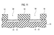
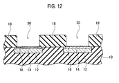
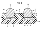
次に、本発明の実施の形態に係る構造体を用いる半導体装置の製造方法を、図9~図13に示す工程断面図を用いて説明する。
図9に示すように、フォトリソグラフィ、エッチング、及びスパッタリング等により、半導体回路等が形成された基板上に形成された配線層(下地層)10に、Cu等の第1導電膜12、及びTiN等の第2導電膜14を形成する。第1及び第2導電膜12、14が配線として用いられる。
図10に示すように、CVD等により配線層10上にSiO2等の絶縁膜18を形成する。
図11に示すように、フォトリソグラフィ、エッチング等により絶縁膜18の一部を選択に除去して貫通孔30を形成する。貫通孔30には、第2導電膜14の表面が露出する。
図12に示すように、物理蒸着等により貫通孔30内に露出した第2導電膜14表面にCo等の触媒層16を形成する。
図13に示すように、図3に示したプラズマCVD装置を用いるプラズマCVD等により、触媒層16上にCNT束20を成長させる。まず、成長温度を約600℃、CH4濃度を約10%、及びグリッド電位を接地としてCNT成長を行う。その後、成長温度を約500℃に下げてCNT成長を行う。その結果、先端部において外周に向かって凸状の曲率を有し、基端部において貫通孔30を埋めこむような形状のCNT束20が形成される。
本発明の実施の形態では、図3に示したように、表面波型の電磁波導入方式によって、反応室6の内部でリモート化されたプラズマを発生させる。そのため、アモルファスカーボン等の生成や触媒層16へのプラズマによるダメージを最小化している。また、表面波型のスリットアンテナ62から導入されたマイクロ波電力により励起された放電活性種に含まれるイオン成分は、CNT成長の際にアモルファスカーボンを生成させる恐れがある。そのため、マイクロ波導入部近傍にイオントラップ64を配置して放電ガスを放電領域76に滞留させてイオン成分を低減する。更に、基板2の近傍には金属製メッシュのグリッド66を設置し、放電領域から拡散してくる電荷成分を中和する。このようにして、貫通孔30内に選択的にCNT束を成長させることが出来る。
ここで、CNT22は、下地の触媒層16により直径及び堆積表面密度が制御される。例えば、レーザアブレーション等によって蒸発させたCo等のクラスタをインパクタ方式等を用いてサイズ分布を整える。このようにして、平均粒径が約5nmのCo等の金属粒子を所望の面密度で堆積させて触媒層16を形成する。あるいは、堆積したCo等の金属薄膜を、所定の温度で加熱して凝集させることにより触媒層16を形成してもよい。
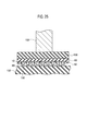
なお、図14に示すように、CNT束20の先端に金属膜40を選択的に設けてもよい。コンタクト電極の先端接触部に炭素以外の材料を任意に選択することができる。また、CNT22個々の微細な針状構造を避ける必要がある場合に有効である。金属膜40は、予めパターニングしたペースト電極を印刷して転写することにより形成することができる。あるいは、マスク蒸着により金属膜40を形成してもよい。
また、本発明の実施の形態に係る構造体をコンタクト電極として用い、パッケージ等の配線と接続させる場合、図15に示すように、基板100上に設けた絶縁膜108に貫通孔115を設けてもよい。貫通孔115の寸法は、CNT束20の外径に合わせる。
図16に示すように、CNT束20の先端部を貫通孔115に嵌め合わせるようにしてCNT束20と導電膜102、104とを接続させる。CNT束20の先端部は直径が小さくなっている。そのため、CNT束20と導電膜102、104との位置合わせやはめ込みをスムーズに行うことができる。また、CNT束20は貫通孔115の外にはみ出してしまう恐れがない。したがって、CNT束20を適切な接触圧で押し込むことができ、CNT束20と導電膜104との良好な接触を得ることができる。これにより、電気的あるいは熱的な導通を高めることが可能となる。
また、図17に示すように、導電膜104の表面にCNT束110を形成してもよい。この場合、導電膜104の表面に形成した触媒層106上にCNT束110を成長させる。図18に示すように、CNT束20とCNT束110とを互いに押し付けるようにして接続させる。CNT束110は、図4に示した第1領域24aだけであってもよい。
また、図19に示すように、絶縁膜108に設けた貫通孔115の中にCNT束110を形成してもよい。この場合、図20に示すように、CNT束20は貫通孔115に嵌め合わせるようにしてCNT束110と接触させる。
図18及び図20に示した構造では、CNT束20、110同士を接触させるため、接触電位差等を生じさせること無く接続することが可能である。また、接触を保持できるストローク幅が広がるため、CNT束20、110の先端高さがばらつく場合にも、押圧を確保しながら、一様に接触させることができる。
(第1の応用例)
本発明の実施の形態の第1の応用例として、CNT束を用いるマイクロスイッチ等のマイクロ電気機械システム(MEMS)装置について説明する。第1の応用例に係るMEMS装置は、図21に示すように、固定電極としてのCNT束20と可動梁122を備える。CNT束20は、基板上の下地層10に設けられた配線126上に配置される。可動梁122は、アンカー124により下地層10上に固定される。下地層10から離間した可動梁122の先端が、CNT束20と対向する。可動梁122の下地層10に対向する表面に可動電極120が設けられる。
本発明の実施の形態の第1の応用例として、CNT束を用いるマイクロスイッチ等のマイクロ電気機械システム(MEMS)装置について説明する。第1の応用例に係るMEMS装置は、図21に示すように、固定電極としてのCNT束20と可動梁122を備える。CNT束20は、基板上の下地層10に設けられた配線126上に配置される。可動梁122は、アンカー124により下地層10上に固定される。下地層10から離間した可動梁122の先端が、CNT束20と対向する。可動梁122の下地層10に対向する表面に可動電極120が設けられる。
可動梁122を静電力、熱応力、電磁力、圧電力等で駆動して屈曲変位させ、CNT束20と接触させることができる。高い電気伝導性及び熱伝導性を有するCNT束20を用いることにより、安定で十分な接触が可能な接点構造を実現することができる。
(第2の応用例)
本発明の実施の形態の第2の応用例では、CNT束を用いる電子装置の電気的特性の検査に用いるプローバのプローブについて説明する。第2の応用例に係るプローブは、図22及び図23に示すように、シリコン(Si)等のリードビーム140上に設けられた配線(導電膜)12と、配線12上に設けられたCNT束20を備える。配線12は、リードビーム140上の下地層10に形成される。CNT束20の基端部は、リードビーム140の先端部において下地層10表面に設けられた絶縁膜18に埋めこまれている。リードビーム140は、プローバのプローブヘッド142に取り付けられる。
本発明の実施の形態の第2の応用例では、CNT束を用いる電子装置の電気的特性の検査に用いるプローバのプローブについて説明する。第2の応用例に係るプローブは、図22及び図23に示すように、シリコン(Si)等のリードビーム140上に設けられた配線(導電膜)12と、配線12上に設けられたCNT束20を備える。配線12は、リードビーム140上の下地層10に形成される。CNT束20の基端部は、リードビーム140の先端部において下地層10表面に設けられた絶縁膜18に埋めこまれている。リードビーム140は、プローバのプローブヘッド142に取り付けられる。
例えば、CNT束20を半導体チップ132表面に設けられたパッド130に接触させて半導体チップ132の動作試験を行うことができる。CNT束20の弾性効果によりパッド130との接触を安定に行うことができ、試験データの信頼性を向上させることが可能となる。
また、複数のリードビームを用いてプローブアレイとしてもよい。例えば、図24に示すように、複数のリードビーム140a、140b、140cのそれぞれの先端部にCNT束20a、20b、20cが設けられる。CNT束20a、20b、20cのそれぞれを半導体チップ132の複数のパッド130a、130b、130cに接触させて動作試験が行われる。CNT束20a、20b、20cの弾性効果により、複数のパッド130a、130b、130cのそれぞれに同時に安定性よく接触させることが可能である。
更に、図25に示すように、プローブピン152の先端に設けた基板150上に、バンプとしてアレイ状に複数のCNT束20を配置してもよい。複数のCNT束20のそれぞれは、基板150上の下地層10に形成された複数の配線12上に、それぞれ配置される。また、複数のCNT束20のそれぞれは、下地層10上に設けられた絶縁膜18に埋めこまれている。複数のCNT束20のそれぞれには弾力性があり、半導体チップ132の複数のパッド130のそれぞれと同時に安定に接触させることができる。
(その他の実施の形態)
上記のように、本発明の実施の形態を記載したが、この開示の一部をなす論述及び図面はこの発明を限定するものであると理解すべきではない。この開示から当業者にはさまざまな代替実施の形態、実施例及び運用技術が明らかとなろう。
上記のように、本発明の実施の形態を記載したが、この開示の一部をなす論述及び図面はこの発明を限定するものであると理解すべきではない。この開示から当業者にはさまざまな代替実施の形態、実施例及び運用技術が明らかとなろう。
本発明の実施の形態においては、CNT束を有する構造体を半導体装置のコンタクト電極に用いているが、半導体装置に限定されず、液晶装置、磁気記録媒体、光記録媒体、薄膜磁気ヘッド、超伝導素子、音響電気変換素子、等の電子装置のコンタクト電極に対しても、本発明が適用できることは、上記説明から容易に理解できるであろう。
このように、本発明はここでは記載していないさまざまな実施の形態等を含むことは勿論である。したがって、本発明の技術的範囲は上記の説明から妥当な特許請求の範囲に係わる発明特定事項によってのみ定められるものである。
本発明は、カーボンナノチューブを用いる構造体及び電子装置に適用できる。
Claims (9)
- 下地層に設けられた導電膜と、
一端を前記導電膜に接続した複数のカーボンナノチューブからなるCNT束とを備え、
前記CNT束の他端側において、前記複数のカーボンナノチューブのうち少なくとも前記CNT束の外側部のカーボンナノチューブが前記CNT束の外に向かって凸の曲率を有して延伸し、前記CNT束の外周に向かうほど前記曲率が大きくなり、前記他端に向かって前記CNT束の直径が小さくなることを特徴とする構造体。 - 前記他端側における前記複数のカーボンナノチューブのそれぞれの長さが、前記CNT束の内側から前記外側に向かって長くなることを特徴とする請求項1に記載の構造体。
- 前記一端側における前記複数のカーボンナノチューブのそれぞれが、蛇行していることを特徴とする請求項1に記載の構造体。
- 前記他端に接続した金属膜を更に備えることを特徴とする請求項1に記載の構造体。
- 前記CNT束が、前記下地層上の絶縁膜中に設けられた貫通孔に配置されることを特徴とする請求項1に記載の構造体。
- 下地層に設けられた第1配線に一端を接続した複数の第1カーボンナノチューブからなる第1CNT束からなり、前記第1CNT束の他端側において、前記複数の第1カーボンナノチューブのうち少なくとも前記第1CNT束の外側部のカーボンナノチューブが前記CNT束の外に向かって凸の曲率を有して延伸し、前記第1CNT束の外周に向かうほど前記曲率が大きくなり、前記第1CNT束の他端に向かって前記第1CNT束の直径が小さくなるコンタクト電極を有する第1基板と、
前記第1基板に対向し、前記コンタクト電極に電気的に接続される第2配線を有する第2基板
とを備えることを特徴とする電子装置。 - 前記第2基板の上に、少なくとも前記第1CNT束の他端側の領域と嵌合する貫通孔を有する絶縁膜が設けられることを特徴とする請求項6に記載の電子装置。
- 前記第2配線に一端を接続した複数の第2カーボンナノチューブからなる第2CNT束を更に備え、該第2CNT束の他端に前記コンタクト電極が接続され、前記第2CNT束の他端側において、前記複数の第2カーボンナノチューブのうち少なくとも前記第2CNT束の外側部のカーボンナノチューブが前記CNT束の外に向かって凸の曲率を有して延伸し、前記第2CNT束の外周に向かうほど前記曲率が大きくなり、前記第2CNT束の他端に向かって前記第2CNT束の直径が小さくなることを特徴とする請求項6に記載の電子装置。
- プラズマが生成される反応室において、下地層に形成された導電膜に一端を接続する複数のカーボンナノチューブからなるCNT束を成長させる構造体の形成方法であって、
前記CNT束の他端側において、前記複数のカーボンナノチューブのうち少なくとも前記CNT束の外側部のカーボンナノチューブが前記CNT束の外に向かって凸の曲率を有して成長し、前記CNT束の外周に向かうほど前記曲率が大きくなり、前記他端に向かって前記CNT束の直径が小さくなるように、成長温度、前記反応室に供給する炭化水素ガスの濃度、及び前記プラズマと前記導電膜の間に設けたグリッドのグリッド電位を設定して前記複数のカーボンナノチューブの第1領域を前記導電膜上に成長させる段階と、
前記導電膜と前記第1領域の間で前記複数のカーボンナノチューブのそれぞれが蛇行するように、前記成長温度を下げること、前記炭化水素ガスの濃度を上げること、及び前記グリッド電位を下げることのうち少なくとも一つを実施して前記複数のカーボンナノチューブの第2領域を成長させる段階
とを含むことを特徴とする構造体の形成方法。
Priority Applications (2)
| Application Number | Priority Date | Filing Date | Title |
|---|---|---|---|
| US13/060,994 US8350160B2 (en) | 2008-08-25 | 2008-08-25 | Structure, electronic device, and method for fabricating a structure |
| PCT/JP2008/065128 WO2010023720A1 (ja) | 2008-08-25 | 2008-08-25 | 構造体、電子装置及び構造体の形成方法 |
Applications Claiming Priority (1)
| Application Number | Priority Date | Filing Date | Title |
|---|---|---|---|
| PCT/JP2008/065128 WO2010023720A1 (ja) | 2008-08-25 | 2008-08-25 | 構造体、電子装置及び構造体の形成方法 |
Publications (1)
| Publication Number | Publication Date |
|---|---|
| WO2010023720A1 true WO2010023720A1 (ja) | 2010-03-04 |
Family
ID=41720909
Family Applications (1)
| Application Number | Title | Priority Date | Filing Date |
|---|---|---|---|
| PCT/JP2008/065128 Ceased WO2010023720A1 (ja) | 2008-08-25 | 2008-08-25 | 構造体、電子装置及び構造体の形成方法 |
Country Status (2)
| Country | Link |
|---|---|
| US (1) | US8350160B2 (ja) |
| WO (1) | WO2010023720A1 (ja) |
Cited By (1)
| Publication number | Priority date | Publication date | Assignee | Title |
|---|---|---|---|---|
| WO2018173884A1 (ja) * | 2017-03-21 | 2018-09-27 | 日本電産リード株式会社 | プローブ構造体、及びプローブ構造体の製造方法 |
Families Citing this family (6)
| Publication number | Priority date | Publication date | Assignee | Title |
|---|---|---|---|---|
| US7827519B2 (en) * | 2006-12-29 | 2010-11-02 | Cadence Design Systems, Inc. | Method, system, and computer program product for preparing multiple layers of semiconductor substrates for electronic designs |
| FR2952048B1 (fr) * | 2009-11-03 | 2011-11-18 | Thales Sa | Micro-commutateur capacitif comportant un drain de charges a base de nanotubes orientes sur l'electrode basse et procede de fabrication |
| JP2011204769A (ja) * | 2010-03-24 | 2011-10-13 | Toshiba Corp | 半導体装置及びその製造方法 |
| US9388731B2 (en) | 2013-03-15 | 2016-07-12 | Kohler Co. | Noise suppression system |
| JP5951568B2 (ja) * | 2013-08-29 | 2016-07-13 | 株式会社東芝 | 半導体装置及びその製造方法 |
| CA3006938C (en) * | 2014-12-10 | 2023-08-15 | Paul D. Okulov | Micro electro-mechanical strain displacement sensor and usage monitoring system |
Citations (3)
| Publication number | Priority date | Publication date | Assignee | Title |
|---|---|---|---|---|
| JP2007279014A (ja) * | 2006-03-13 | 2007-10-25 | Serubakku:Kk | 集積回路検査装置およびその製造方法 |
| JP2008137846A (ja) * | 2006-12-01 | 2008-06-19 | Fujitsu Ltd | 炭素細長構造束状体、その製造方法および電子素子 |
| JP2008210954A (ja) * | 2007-02-26 | 2008-09-11 | Fujitsu Ltd | カーボンナノチューブバンプ構造体とその製造方法、およびこれを用いた半導体装置 |
Family Cites Families (9)
| Publication number | Priority date | Publication date | Assignee | Title |
|---|---|---|---|---|
| US6232706B1 (en) * | 1998-11-12 | 2001-05-15 | The Board Of Trustees Of The Leland Stanford Junior University | Self-oriented bundles of carbon nanotubes and method of making same |
| US6297063B1 (en) * | 1999-10-25 | 2001-10-02 | Agere Systems Guardian Corp. | In-situ nano-interconnected circuit devices and method for making the same |
| JP4212258B2 (ja) | 2001-05-02 | 2009-01-21 | 富士通株式会社 | 集積回路装置及び集積回路装置製造方法 |
| US8048688B2 (en) * | 2006-10-24 | 2011-11-01 | Samsung Electronics Co., Ltd. | Method and apparatus for evaluation and improvement of mechanical and thermal properties of CNT/CNF arrays |
| US7135773B2 (en) * | 2004-02-26 | 2006-11-14 | International Business Machines Corporation | Integrated circuit chip utilizing carbon nanotube composite interconnection vias |
| US20050285116A1 (en) * | 2004-06-29 | 2005-12-29 | Yongqian Wang | Electronic assembly with carbon nanotube contact formations or interconnections |
| JP4855757B2 (ja) | 2005-10-19 | 2012-01-18 | 富士通株式会社 | カーボンナノチューブパッド及び電子デバイス |
| KR100813243B1 (ko) * | 2006-07-04 | 2008-03-13 | 삼성에스디아이 주식회사 | 탄소나노튜브를 이용한 반도체 소자의 층간 배선 및 그제조 방법 |
| US8063483B2 (en) * | 2007-10-18 | 2011-11-22 | International Business Machines Corporation | On-chip temperature gradient minimization using carbon nanotube cooling structures with variable cooling capacity |
-
2008
- 2008-08-25 US US13/060,994 patent/US8350160B2/en active Active
- 2008-08-25 WO PCT/JP2008/065128 patent/WO2010023720A1/ja not_active Ceased
Patent Citations (3)
| Publication number | Priority date | Publication date | Assignee | Title |
|---|---|---|---|---|
| JP2007279014A (ja) * | 2006-03-13 | 2007-10-25 | Serubakku:Kk | 集積回路検査装置およびその製造方法 |
| JP2008137846A (ja) * | 2006-12-01 | 2008-06-19 | Fujitsu Ltd | 炭素細長構造束状体、その製造方法および電子素子 |
| JP2008210954A (ja) * | 2007-02-26 | 2008-09-11 | Fujitsu Ltd | カーボンナノチューブバンプ構造体とその製造方法、およびこれを用いた半導体装置 |
Cited By (2)
| Publication number | Priority date | Publication date | Assignee | Title |
|---|---|---|---|---|
| WO2018173884A1 (ja) * | 2017-03-21 | 2018-09-27 | 日本電産リード株式会社 | プローブ構造体、及びプローブ構造体の製造方法 |
| JPWO2018173884A1 (ja) * | 2017-03-21 | 2020-01-30 | 日本電産リード株式会社 | プローブ構造体、及びプローブ構造体の製造方法 |
Also Published As
| Publication number | Publication date |
|---|---|
| US20110147177A1 (en) | 2011-06-23 |
| US8350160B2 (en) | 2013-01-08 |
Similar Documents
| Publication | Publication Date | Title |
|---|---|---|
| KR100813243B1 (ko) | 탄소나노튜브를 이용한 반도체 소자의 층간 배선 및 그제조 방법 | |
| US6764874B1 (en) | Method for chemical vapor deposition of single walled carbon nanotubes | |
| CN100568436C (zh) | 碳纳米管发射器及利用其的场发射器件及它们的制造方法 | |
| KR100376768B1 (ko) | 전자, 스핀 및 광소자 응용을 위한 탄소나노튜브의 선택적 수평성장 방법 | |
| US8350160B2 (en) | Structure, electronic device, and method for fabricating a structure | |
| JP4773317B2 (ja) | 電界放出装置及びその製造方法 | |
| US8476994B2 (en) | Electromechanical switch and method of manufacturing the same | |
| JP5636654B2 (ja) | カーボンナノチューブシート構造体およびその製造方法、半導体装置 | |
| US20080169563A1 (en) | Semiconductor package and method of manufacturing the same | |
| TW200913105A (en) | Connecting and bonding adjacent layers with nanostructures | |
| US20060292848A1 (en) | Method for manufacturing nano-gap electrode device | |
| US7989286B2 (en) | Electronic devices using carbon nanotubes having vertical structure and the manufacturing method thereof | |
| CN101313092B (zh) | 基于纳米结构的互联线和散热器 | |
| JP5013116B2 (ja) | シート状構造体及びその製造方法並びに電子機器 | |
| US20100018747A1 (en) | Conductive Nanowires For Electrical Interconnect | |
| JP3222179B2 (ja) | 回路測定用端子およびその製造方法 | |
| JP4635030B2 (ja) | 構造体、電子装置及び構造体の形成方法 | |
| KR101111127B1 (ko) | 시트 형상 구조체와 그 제조 방법 및 전자기기 | |
| US20140287909A1 (en) | Method of forming nano-pads of catalytic metal for growth of single-walled carbon nanotubes | |
| KR100803194B1 (ko) | 탄소나노튜브 구조체 형성방법 | |
| JP2005111583A (ja) | ナノメータスケールの構造物の作製方法 | |
| CN101027742B (zh) | 碳纳米管装置及其制造方法 | |
| US7645482B2 (en) | Method to make and use long single-walled carbon nanotubes as electrical conductors | |
| JP5444912B2 (ja) | 電子機器及びその製造方法 | |
| US7718224B2 (en) | Synthesis of single-walled carbon nanotubes |
Legal Events
| Date | Code | Title | Description |
|---|---|---|---|
| 121 | Ep: the epo has been informed by wipo that ep was designated in this application |
Ref document number: 08809288 Country of ref document: EP Kind code of ref document: A1 |
|
| WWE | Wipo information: entry into national phase |
Ref document number: 13060994 Country of ref document: US |
|
| NENP | Non-entry into the national phase |
Ref country code: DE |
|
| NENP | Non-entry into the national phase |
Ref country code: JP |
|
| 122 | Ep: pct application non-entry in european phase |
Ref document number: 08809288 Country of ref document: EP Kind code of ref document: A1 |