WO2010010761A1 - 絶縁型スイッチング電源装置 - Google Patents
絶縁型スイッチング電源装置 Download PDFInfo
- Publication number
- WO2010010761A1 WO2010010761A1 PCT/JP2009/060734 JP2009060734W WO2010010761A1 WO 2010010761 A1 WO2010010761 A1 WO 2010010761A1 JP 2009060734 W JP2009060734 W JP 2009060734W WO 2010010761 A1 WO2010010761 A1 WO 2010010761A1
- Authority
- WO
- WIPO (PCT)
- Prior art keywords
- secondary winding
- capacitor
- series
- circuit
- switch circuit
- Prior art date
- Legal status (The legal status is an assumption and is not a legal conclusion. Google has not performed a legal analysis and makes no representation as to the accuracy of the status listed.)
- Ceased
Links
Images














Classifications
-
- H—ELECTRICITY
- H02—GENERATION; CONVERSION OR DISTRIBUTION OF ELECTRIC POWER
- H02M—APPARATUS FOR CONVERSION BETWEEN AC AND AC, BETWEEN AC AND DC, OR BETWEEN DC AND DC, AND FOR USE WITH MAINS OR SIMILAR POWER SUPPLY SYSTEMS; CONVERSION OF DC OR AC INPUT POWER INTO SURGE OUTPUT POWER; CONTROL OR REGULATION THEREOF
- H02M1/00—Details of apparatus for conversion
- H02M1/12—Arrangements for reducing harmonics from AC input or output
- H02M1/126—Arrangements for reducing harmonics from AC input or output using passive filters
-
- H—ELECTRICITY
- H02—GENERATION; CONVERSION OR DISTRIBUTION OF ELECTRIC POWER
- H02M—APPARATUS FOR CONVERSION BETWEEN AC AND AC, BETWEEN AC AND DC, OR BETWEEN DC AND DC, AND FOR USE WITH MAINS OR SIMILAR POWER SUPPLY SYSTEMS; CONVERSION OF DC OR AC INPUT POWER INTO SURGE OUTPUT POWER; CONTROL OR REGULATION THEREOF
- H02M1/00—Details of apparatus for conversion
- H02M1/14—Arrangements for reducing ripples from DC input or output
-
- H—ELECTRICITY
- H02—GENERATION; CONVERSION OR DISTRIBUTION OF ELECTRIC POWER
- H02M—APPARATUS FOR CONVERSION BETWEEN AC AND AC, BETWEEN AC AND DC, OR BETWEEN DC AND DC, AND FOR USE WITH MAINS OR SIMILAR POWER SUPPLY SYSTEMS; CONVERSION OF DC OR AC INPUT POWER INTO SURGE OUTPUT POWER; CONTROL OR REGULATION THEREOF
- H02M3/00—Conversion of DC power input into DC power output
- H02M3/22—Conversion of DC power input into DC power output with intermediate conversion into AC
- H02M3/24—Conversion of DC power input into DC power output with intermediate conversion into AC by static converters
- H02M3/28—Conversion of DC power input into DC power output with intermediate conversion into AC by static converters using discharge tubes with control electrode or semiconductor devices with control electrode to produce the intermediate AC
- H02M3/325—Conversion of DC power input into DC power output with intermediate conversion into AC by static converters using discharge tubes with control electrode or semiconductor devices with control electrode to produce the intermediate AC using devices of a triode or a transistor type requiring continuous application of a control signal
- H02M3/335—Conversion of DC power input into DC power output with intermediate conversion into AC by static converters using discharge tubes with control electrode or semiconductor devices with control electrode to produce the intermediate AC using devices of a triode or a transistor type requiring continuous application of a control signal using semiconductor devices only
- H02M3/33569—Conversion of DC power input into DC power output with intermediate conversion into AC by static converters using discharge tubes with control electrode or semiconductor devices with control electrode to produce the intermediate AC using devices of a triode or a transistor type requiring continuous application of a control signal using semiconductor devices only having several active switching elements
- H02M3/33571—Half-bridge at primary side of an isolation transformer
-
- H—ELECTRICITY
- H02—GENERATION; CONVERSION OR DISTRIBUTION OF ELECTRIC POWER
- H02M—APPARATUS FOR CONVERSION BETWEEN AC AND AC, BETWEEN AC AND DC, OR BETWEEN DC AND DC, AND FOR USE WITH MAINS OR SIMILAR POWER SUPPLY SYSTEMS; CONVERSION OF DC OR AC INPUT POWER INTO SURGE OUTPUT POWER; CONTROL OR REGULATION THEREOF
- H02M3/00—Conversion of DC power input into DC power output
- H02M3/22—Conversion of DC power input into DC power output with intermediate conversion into AC
- H02M3/24—Conversion of DC power input into DC power output with intermediate conversion into AC by static converters
- H02M3/28—Conversion of DC power input into DC power output with intermediate conversion into AC by static converters using discharge tubes with control electrode or semiconductor devices with control electrode to produce the intermediate AC
- H02M3/325—Conversion of DC power input into DC power output with intermediate conversion into AC by static converters using discharge tubes with control electrode or semiconductor devices with control electrode to produce the intermediate AC using devices of a triode or a transistor type requiring continuous application of a control signal
- H02M3/335—Conversion of DC power input into DC power output with intermediate conversion into AC by static converters using discharge tubes with control electrode or semiconductor devices with control electrode to produce the intermediate AC using devices of a triode or a transistor type requiring continuous application of a control signal using semiconductor devices only
- H02M3/33569—Conversion of DC power input into DC power output with intermediate conversion into AC by static converters using discharge tubes with control electrode or semiconductor devices with control electrode to produce the intermediate AC using devices of a triode or a transistor type requiring continuous application of a control signal using semiconductor devices only having several active switching elements
- H02M3/33573—Full-bridge at primary side of an isolation transformer
-
- H—ELECTRICITY
- H02—GENERATION; CONVERSION OR DISTRIBUTION OF ELECTRIC POWER
- H02M—APPARATUS FOR CONVERSION BETWEEN AC AND AC, BETWEEN AC AND DC, OR BETWEEN DC AND DC, AND FOR USE WITH MAINS OR SIMILAR POWER SUPPLY SYSTEMS; CONVERSION OF DC OR AC INPUT POWER INTO SURGE OUTPUT POWER; CONTROL OR REGULATION THEREOF
- H02M3/00—Conversion of DC power input into DC power output
- H02M3/01—Resonant DC/DC converters
Definitions
- the present invention relates to an isolated switching power supply apparatus that uses a composite transformer having a plurality of secondary windings and uses its leakage inductance to eliminate the need for an external choke coil.
- a low-pass filter for smoothing an output current is generally composed of an external inductor and a smoothing capacitor.
- By deliberately reducing the degree of magnetic coupling of the transformer In addition, techniques for increasing leakage inductance are also known. Patent Documents 1 to 4 are shown as examples of these.
- Patent Document 1 is configured such that a leakage gap is intentionally generated by providing a core gap GAP4 in the core of the insulating transformer T2, and an external inductor L is provided. The size can be reduced.
- Patent Document 2 has an isolation transformer in which both the primary winding and the secondary winding have N turns, and the inductor L2 is intentionally increased from the isolation transformer. The leakage inductance is used.
- Patent Document 3 as shown in FIG. 3, the primary winding 5a and the tertiary winding 5c of the transformer T1 are loosely coupled, the leakage inductance of the tertiary winding 5c is increased, and the external inductor is externally seen. It is a technology that can be eliminated.
- Patent Document 4 is a technique that eliminates the need for an external choke coil by utilizing the leakage inductance L1 of the transformer T as shown in FIG. JP 2001-218457 A Special Table 2003-533163 International Publication WO2004 / 019472 Pamphlet JP 2007-43858 A
- the insulating switching power supply devices disclosed in Patent Documents 1 to 4 have a fundamental problem. That is, when the leakage inductance of the transformer is used as an output current smoothing inductor, the inductance value is small only with the leakage inductance, and the output current ripple is large because the ability to smooth the output current is low.
- the on-time ratio of the primary side switch element changes in order to control the output voltage, and the voltage generated in the secondary winding during the on period of the primary side switch element and the voltage generated in the secondary winding during the off period. As the difference between and increases, the output current ripple increases.
- the magnetic coupling degree of the transformer is intentionally reduced by, for example, providing an air gap in the transformer core in an attempt to increase the leakage inductance value, the inductance value for energy transmission is also reduced. This will increase the size of the transformer itself.
- an object of the present invention is to eliminate the above-mentioned problems, and without using a choke coil as an external inductor, and can sufficiently reduce output current ripple, and is an insulation type switching using a relatively small transformer. It is to provide a power supply device.
- the present invention is configured as follows to solve the above-described problems.
- a DC power input unit to which a DC input voltage Vi is input; At least a first primary winding np, a first secondary winding ns, a second secondary winding nf1, and a third secondary winding nf2 that are magnetically coupled are provided.
- a first transformer T A first switching circuit S1 including a parallel circuit of a first switching element Q1, a first capacitor C1, and a first diode D1, A series circuit composed of the first primary winding np and the first switch circuit S1 connected in series to the DC power supply input unit;
- a first inductor Lrf1 formed as a leakage inductance in series with the second secondary winding nf1, The second inductor Lrf2, which is formed as a leakage inductance in series with the third secondary winding nf2, the first inductance Lrf1, the second inductor Lrf2, and the second inductor constituting the low-pass filter.
- An insulated switching power supply device configured to transmit energy from a primary side to a secondary side in accordance with an on / off operation of the first switch circuit S1,
- the second secondary winding nf1 and the third secondary winding nf2 are wound so that the number of turns is equal to each other and their magnetic polarities are opposite to each other.
- the first secondary winding ns, the second secondary winding nf1, and the third secondary winding nf2 are connected in series to form a closed loop with the first capacitor Co;
- the output voltage Vo is output from the output terminal of the low pass filter.
- the first primary winding np and the first secondary winding ns are wound such that their magnetic polarities are the same, A second diode Ds that is turned on while the first switch circuit S1 is on; A forward converter having a third diode Df that is turned on while the first switch circuit S1 is off is configured.
- the first primary winding np and the first secondary winding ns are wound so that their magnetic polarities are opposite to each other,
- the first secondary winding ns includes a first diode Ds that is turned on during a period in which the first switch circuit S1 is turned off;
- a flyback converter having a rectifying and smoothing circuit comprising: a third capacitor Co1 that discharges during a period when the first switch circuit S1 is on and charges during a period when the first switch circuit S1 is off. It is characterized by comprising.
- a fourth capacitor Cr comprising a parallel circuit of a second switching element Q2, a fifth capacitor C2, and a fourth diode D2, A third inductor Lr connected in series with the first primary winding np and formed as a leakage inductance in series with the first primary winding np; A series circuit composed of the first primary winding np and the first switch circuit S1 is connected to the DC power supply input unit, A series circuit including the fourth capacitor and the second switch circuit S2 is configured to be connected in parallel to the first primary winding np or the first switch circuit S1.
- a second switch circuit S2 composed of a parallel circuit of a second switching element Q2, a fifth capacitor C2, and a fourth diode D2, A sixth capacitor Cr1, A seventh capacitor Cr2, A third inductor Lr connected in series to the first primary winding np and formed as a leakage inductance in series with the first primary winding np;
- a series circuit composed of the first switch circuit S1 and the second switch circuit S2 and a series circuit composed of the sixth capacitor Cr1 and the seventh capacitor Cr2 are parallel to the DC power supply input unit. Connected, Between the connection point between the first switch circuit S1 and the second switch circuit S2 and the connection point between the sixth capacitor Cr1 and the seventh capacitor Cr2, the first primary winding is provided.
- a half bridge circuit is configured by connecting the line np.
- a second switch circuit S2 composed of a parallel circuit of a second switching element Q2, a fifth capacitor C2, and a fourth diode D2,
- a third switching circuit S3 comprising a parallel circuit of a third switching element Q3, an eighth capacitor C3, and a fifth diode D3;
- a fourth switching circuit S4 comprising a parallel circuit of a fourth switching element Q4, a ninth capacitor C4, and a sixth diode D4;
- a third inductor Lr connected in series with the first primary winding np and formed as a leakage inductance in series with the first primary winding np;
- the first 1 A full bridge circuit is configured by connecting the next winding np.
- the first primary winding np includes a second primary winding np1 and a third primary winding np2 whose one ends are connected to each other.
- a second switching circuit S2 composed of a parallel circuit of a second switching element Q2, a fifth capacitor C2, and a fourth diode D2,
- a series circuit composed of the second primary winding np1 and the second switch circuit S2 with respect to the DC power supply input unit;
- a series circuit including the third primary winding np2 and the first switch circuit S1 is connected in parallel to each other.
- the transformer T further including a fourth primary winding ni and a fourth secondary winding no;
- a second switch circuit S2 comprising a parallel circuit of a second switching element Q2, a fifth capacitor C2, and a fourth diode D2, A fourth capacitor Cr; A tenth capacitor Ce;
- a third inductor Lr connected in series with the first primary winding np and formed as a leakage inductance in series with the first primary winding np;
- a fourth inductor Lri connected in series with the fourth primary winding ni and formed as a leakage inductance in series with the fourth primary winding ni; From the DC power supply input unit, a series circuit including the fourth primary winding ni and the first switch circuit S1, a first primary winding np, and the tenth capacitor Ce Are connected in parallel to each other,
- a series circuit composed of the second switch circuit S2 and the fourth capacitor Cr is connected in parallel to the first primary winding np or the first switch circuit S1. .
- the transformer T is wound so that energy transmission is performed from the primary side to the secondary side in a period in which the first switch circuit S1 is on and the second switch circuit S2 is off.
- the first secondary winding ns and the fourth secondary winding no are connected in series,
- a fifth inductor Lro formed as a leakage inductance in series with the fourth secondary winding no;
- a second diode Ds that is turned on while the first switch circuit S1 is on;
- a third diode Df that is turned on while the first switch circuit S1 is turned off is connected.
- One end of the first secondary winding ns and the fourth secondary winding no are commonly connected, and the other end is connected to the second diode Ds or the third diode Df.
- a center tap type rectifier circuit is configured.
- a second diode Ds having a cathode connected to one end of the first secondary winding ns and an anode connected to one end of the eleventh capacitor;
- a third diode Df having an anode connected to the one end of the first secondary winding ns and a cathode connected to a third capacitor Co1;
- a voltage doubler rectifier circuit is configured by connecting the other end of the eleventh capacitor Co2 and the other end of the third capacitor Co1 to the other end of the first secondary winding ns.
- the second secondary winding nf1 is connected between one end of the first secondary winding ns and a high potential side terminal of the second capacitor Co, and the third secondary winding The winding nf2 is connected between the other end of the first secondary winding ns and the low potential side terminal of the second capacitor Co.
- the first transformer T further includes a fifth secondary winding nf3 and a sixth secondary winding nf4.
- the fifth secondary winding nf3 and the sixth secondary winding nf4 are wound so that the number of turns is equal to each other and the magnetic polarities of the fifth secondary winding nf3 are opposite to each other.
- the second secondary winding nf1, the third secondary winding nf2, the fifth secondary winding nf3, and the sixth secondary winding nf4 are the first secondary winding Connected in series to the winding ns, A sixth inductor Lrf3 formed as a leakage inductance in series with the fifth secondary winding nf3, connected in series with the fifth secondary winding nf3; A seventh inductor Lrf4 formed as a leakage inductance in series with the sixth secondary winding nf4, connected in series with the sixth secondary winding nf4; A second capacitor Co constituting a first low pass filter together with the sixth inductance Lrf3 and the seventh inductor Lrf4; The second inductor Lrf1 and the third capacitor Co1 that forms a second low-pass filter together with the third inductor Lrf2.
- the output voltage Vo is output from the output terminal of the first low pass filter.
- the first transformer T further includes a fifth secondary winding nf3 and a sixth secondary winding nf4.
- the fifth secondary winding nf3 and the sixth secondary winding nf4 are wound so that the number of turns is equal to each other and the magnetic polarities of the fifth secondary winding nf3 are opposite to each other.
- the second secondary winding nf1, the third secondary winding nf2, the fifth secondary winding nf3, and the sixth secondary winding nf4 are the first secondary winding Connected in series to the winding ns, A fifth inductor Lro formed as a leakage inductance in series with the fourth secondary winding no in series with the fourth secondary winding no; A sixth inductor Lrf3 formed as a leakage inductance in series with the fifth secondary winding nf3 in series with the fifth secondary winding nf3;
- the seventh inductor Lrf4 configured by the leakage inductance of the sixth secondary winding nf4 in series with the sixth secondary winding nf4, the sixth inductance Lrf3, and the seventh inductor Lrf4
- an eleventh capacitor Co2 constitu
- the magnetic component can be only a transformer, it is not necessary to use an external inductor, and the switching power supply device can be downsized.
- the secondary windings nf1 and nf2 can reduce switching noise when the transformer voltage is inverted.
- the resistance to the common mode noise is enhanced by connecting the secondary windings nf1 and nf2 to the high potential side and the low potential side of the secondary winding ns or ns and no, respectively.
- FIG. 1 is a circuit diagram of an insulating switching power supply device disclosed in Patent Document 1.
- FIG. It is a circuit diagram of an insulation type switching power supply device shown in patent documents 2. It is a circuit diagram of an insulation type switching power supply device shown in patent documents 3. It is a circuit diagram of an insulation type switching power supply device shown in patent documents 4.
- 1 is a circuit diagram of an insulated switching power supply device according to a first embodiment. It is a circuit diagram of the insulation type switching power supply device concerning a 2nd embodiment. It is a circuit diagram of the insulation type switching power supply device concerning a 3rd embodiment. It is a wave form diagram of the insulation type switching power supply device concerning a 3rd embodiment. It is a circuit diagram of the insulation type switching power supply device concerning a 4th embodiment.
- transformer used for the insulation type switching power supply device concerning a 13th embodiment. It is another structural example of the transformer used for the insulation type switching power supply device concerning a 14th embodiment. It is the other structural example of the transformer used for the insulation type switching power supply device which concerns on 15th Embodiment. It is another structural example of the transformer used for the insulation type switching power supply device according to the sixteenth embodiment. It is another structural example of the transformer used for the insulation type switching power supply device according to the seventeenth embodiment. It is another structural example of the transformer used for the insulation type switching power supply device concerning the 18th embodiment. It is another structural example of the transformer used for the insulation type switching power supply device according to the nineteenth embodiment.
- transformer used for the insulation type switching power supply device concerning a 20th embodiment. It is another structural example of the transformer used for the insulation type switching power supply device concerning a 21st embodiment. It is another structural example of the transformer used for the insulation type switching power supply device concerning a 22nd embodiment.
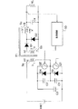
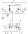
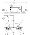
- FIG. 5 is a circuit diagram of the isolated switching power supply device according to the first embodiment.
- the insulated switching power supply device includes a first primary winding np and a first switch circuit S1 connected in series to both ends of a DC power supply input unit to which a DC input voltage Vi is input.
- the circuit is connected.
- the first primary winding np forms a composite transformer T with the first secondary winding ns, the second secondary winding nf1, and the third secondary winding nf2.
- One end of the first secondary winding ns is connected to one end of the second secondary winding nf1 and the cathode of the third diode Df, and the other end is connected to the cathode of the second diode Ds.
- the second secondary winding nf1 has one end connected to the high potential side of the first secondary winding ns and the other end connected to the high potential side of the output terminal.
- the third secondary winding nf2 has one end connected to the anode of the third diode Df and the anode of the second diode Ds, and the other end connected to the low potential side of the output terminal.
- a second capacitor Co that is a smoothing capacitor is connected in parallel between the output terminals.
- the first primary winding np and the first secondary winding ns are configured to be a forward type.
- the second secondary winding nf1 and the third secondary winding nf2 are wound so that the number of turns is equal to each other and the magnetic polarity is opposite to each other. The resulting voltage is canceled out.
- the magnetic flux not interlinked with the third secondary winding nf2 acts as a first inductor Lrf1 that is a leakage inductance.
- the magnetic flux not interlinked with the second secondary winding nf1 acts as a second inductor Lrf2 that is a leakage inductance.
- the first switch circuit S1 is configured by a parallel connection circuit of a first switching element Q1, a first diode D1, and a first capacitor C1.
- the first switching element Q1 By configuring the first switching element Q1 with a field effect transistor such as a MOSFET, it is possible to use the parasitic diode as the first diode D1 and the parasitic capacitor as the first capacitor C1. As a result, the mounting as these individual components can be omitted, and the number of components can be reduced.
- a field effect transistor such as a MOSFET
- the on / off timing of the first switching element Q1 includes, for example, an output voltage detection circuit for detecting an output voltage, and an insulation feedback means such as a photocoupler is used when a predetermined voltage is exceeded. On / off control is performed based on the feedback.
- the switching frequency is constant, so that frequency components such as EMI noise generated by the switching operation are also concentrated on the constant frequency. There is an advantage that it is easy to take measures against noise.
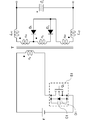
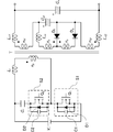
- FIG. 6 is a circuit diagram of an isolated switching power supply device according to the second embodiment.
- the first primary winding np and the first secondary winding ns in the first embodiment have opposite magnetic polarities. Polarity. That is, while the first embodiment is a forward method, the second embodiment is a flyback method. Accordingly, the third diode Df becomes unnecessary, but it is preferable to connect the third capacitor Co1 instead of the third diode Df in order to effectively reduce the current ripple.
- a circuit configuration in which the second secondary winding nf1, the first inductance Lrf1, and the low-pass filter by the second capacitor Co are inserted becomes more current. Ripple can be reduced.
- the third secondary is output during the period when the first switch circuit S1 including the parallel circuit of the first switching element Q1, the first diode D1, and the first capacitor C1 is on.
- a current flows in the order of the winding nf2 ⁇ the third capacitor Co1 ⁇ the second secondary winding nf1, and the energy charged in the third capacitor Co1 and the second capacitor Co2 is output to the output terminal.
- the second secondary winding nf2 ⁇ the second diode Ds ⁇ the first secondary winding ns ⁇ the second secondary winding nf1.
- a current flows in order, and only the voltage generated in the first secondary winding ns is output to the output terminal.
- the effects of the configuration of the insulated switching power supply according to the second embodiment are the effects (a), (c), (d), (e), and (f) among the effects mentioned in the first embodiment. , (G).
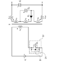
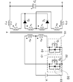
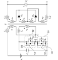
- FIG. 7 is a circuit diagram of an isolated switching power supply device according to the third embodiment.
- this isolated switching power supply device includes a third inductor Lr and a first primary winding with respect to the + side terminal and the ⁇ side terminal of the power input unit to which the DC voltage Vi is supplied.
- a series circuit including the line np and the first switch circuit S1 is connected, and the connection point between the fourth capacitor Cr and the first switch circuit S1, the fourth capacitor Cr, and the second switch circuit S2. Is connected in parallel to either the first primary winding np or the first switch circuit S2.
- the first switch circuit S1 includes a parallel connection circuit of a first switching element Q1, a first diode D1, and a first capacitor C1
- the second switch circuit S2 includes a second switch circuit S2.
- the switching element Q2, a fourth diode D2, and a fifth capacitor C2 are connected in parallel.
- the parasitic diodes are the first diode D1 and the fourth diode D2, and the parasitic capacitor is the first capacitor. It can be used as C1 and the fifth capacitor C2. As a result, the mounting as these individual components can be omitted, and the number of components can be reduced.
- the first switch circuit S1 and the second switch circuit S2 are short-circuited when both are turned on at the same time. Therefore, the first switch circuit S1 and the second switch circuit S2 are configured to be complementarily turned on / off with a minimum dead time. Is done.
- the secondary side of the composite transformer T is provided with a first secondary winding ns and a fourth secondary winding no, and the first primary winding np and the first 1
- the next winding ns is wound so as to have the same polarity, and the first primary winding np and the fourth secondary winding no have opposite polarities.
- One end of the first secondary winding ns of the composite transformer T is connected to the cathode of the second diode Ds, and the other end of the first secondary winding ns is connected to the cathode of the third diode Df.
- the anode of the third diode Df is connected to the anode of the second diode Ds.
- One end of the fourth secondary winding no is connected to the cathode of the fourth diode Df and one end of the first secondary winding ns, and the other end of the fourth secondary winding no is the third end. Connected to one end of the secondary winding nf2.
- a smoothing second capacitor Co is connected in parallel between the output terminals.
- the first primary winding np and the first secondary winding ns in the composite transformer T are periods in which the first switch circuit S1 is on and the second switch circuit S2 is off.
- the fourth secondary winding no the first switch circuit S1 is turned off and the second switch circuit S2 is turned on. Since the polarity of the winding is set so as to operate as a flyback system that sends power to the output during the period, the first switch circuit S1 is on and the second switch circuit S2 is off. Current flows in the order of two diodes Ds ⁇ first secondary winding ns ⁇ fourth secondary winding no ⁇ third secondary winding nf2 ⁇ second secondary winding nf1. Supplied.
- the second secondary winding nf1 and the third secondary winding nf2 include the first secondary winding ns ⁇ the fourth secondary winding no ⁇ the third secondary winding.
- the winding nf2 ⁇ the second secondary winding nf1 are connected in this order.
- the composite transformer T energy transmission from the primary side to the secondary side can be realized in either the on period or the off period of the first switch circuit S1, so that the minimum dead time is necessary. Except for, energy transmission from the primary side to the secondary side can be performed over substantially the entire switching period. Furthermore, in the dead time period that is a short period during which the transmission path is switched, the first inductor Lrf1, the second inductor Lrf2, and the fifth inductor Lro that can be configured by the leakage flux of the transformer can suppress the current fluctuation, and thus output. Ripple noise can be greatly reduced, and the second capacitor Co for smoothing can be reduced in size.
- the third inductor Lr is also a leakage inductance formed in series with the primary winding np by the leakage flux of the transformer. As a result, the noise component superimposed on the DC input voltage Vi can be reduced.
- the voltage induced in the first secondary winding ns is Vo1
- the voltage induced in the second secondary winding no is Vo2
- the effects of the configuration of the insulated switching power supply according to the third embodiment are the effects (a), (b), (c), (d), and (e) among the effects mentioned in the first embodiment. , (F).
- FIG. 8 is a waveform diagram of each part of the circuit of the insulated switching power supply device shown in FIG. The circuit operation will be described below with reference to FIG.
- vgs1 and vgs2 are the gate-source voltages of the switching elements Q1 and Q2, respectively, and are waveforms that substantially represent the on / off states of the switching elements Q1 and Q2.
- vds1 and vds2 are the drain-source voltages of the switching elements Q1 and Q2, respectively, and are substantially voltage waveforms across the capacitors C1 and C2.
- id1, id2, ip, and iL are current waveforms of currents flowing through the switch circuits S1, S2, the first primary winding np, and the fifth inductor Lro, respectively.
- the operation in the rated operation of this insulated switching power supply device can be divided into six operation states from time t1 to t7 in one switching cycle Ts.
- the circuit operation will be described below for each state.
- the current flowing to the secondary side of the composite transformer T is as follows: the third diode Ds ⁇ the first secondary winding ns ⁇ the fifth inductor Lro ⁇ the third secondary winding nf2 ⁇ the second inductor Lrf2 ⁇ The second secondary winding nf1 flows in the order of the first inductor Lrf1.
- the current flowing to the secondary side of the composite transformer T is the fourth diode Df ⁇ the fourth secondary winding no ⁇ the fifth inductor Lro ⁇ the third secondary winding nf2 ⁇ the second inductor Lrf2 ⁇
- the second secondary winding nf1 flows in the order of the first inductor Lrf1.
- the on / off timing of the first switching element Q1 and the second switching element Q2 has, for example, an output voltage detection circuit for detecting the output voltage, and a photo that exceeds a predetermined voltage is detected. Feedback is performed using an insulating feedback means such as a coupler, and on / off control is performed based on the feedback.
- the switching frequency is constant, so that frequency components such as EMI noise generated by the switching operation are also concentrated on the constant frequency. There is an advantage that it is easy to take measures against noise.
- PWM pulse amplitude modulation
- PFM pulse frequency modulation
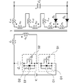
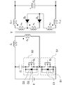
- FIG. 9 is a circuit diagram of an isolated switching power supply device according to the fourth embodiment.
- the secondary circuit is a center tap rectifier circuit. That is, in FIG. 9, the first secondary winding ns and the fourth secondary winding no are wound with the same polarity, one end is commonly connected, and the other ends are the second diode Ds and the third diode, respectively. Commonly connected via Df.
- the second secondary winding nf1 has one end connected to the high potential side of the output terminal and the other end connected to the cathodes of the second diode Ds and the third diode Df.
- the third secondary winding nf2 has one end connected to the low potential side of the output terminal and the other end connected to the common connection point of the first secondary winding ns and the fourth secondary winding no. ing.
- the first switch circuit S1 is on, the second switch circuit S2 is off, and the first switch circuit S1 is off, so that the second switch circuit S2 is off.
- Energy transmission from the primary side to the secondary side can be performed in both periods when is on.
- the effects of the configuration of the insulated switching power supply according to the fourth embodiment are the effects (a), (b), (c), (d), (e) among the effects mentioned in the first embodiment. , (F).
- FIG. 10 is a circuit diagram of an isolated switching power supply device according to the fifth embodiment.
- the difference from the circuit shown in FIG. 7 is the connection order of the second secondary winding nf1 and the third secondary winding nf2. That is, in FIG. 10, the second secondary winding nf1 is on the high potential side and the third secondary winding nf2 is between the first secondary winding ns and the fourth secondary winding no. Connected to the low potential side.
- the effects of the configuration of the insulated switching power supply according to the fifth embodiment are the effects (a), (b), (c), (d), and (e) among the effects mentioned in the first embodiment. , (F).
- FIG. 11 is a circuit diagram of an isolated switching power supply device according to the sixth embodiment.
- the primary circuit is a half-bridge circuit. That is, a series circuit composed of the first switch circuit S1 and the second switch circuit S2 and a series circuit composed of the sixth capacitor Cr1 and the seventh capacitor Cr2 are connected in parallel to the DC input voltage Vi.
- One end of the first primary winding np is connected to the connection point of the first switch circuit S1 and the second switch circuit S2, and the other end is connected to the connection point of the sixth capacitor Cr1 and the seventh capacitor Cr2. It is connected. Since other points are the same as those in the first embodiment, description thereof will be omitted.
- the effects of the configuration of the insulated switching power supply according to the sixth embodiment are the effects (a), (b), (c), (d), and (e) among the effects mentioned in the first embodiment. , (F).
- FIG. 12 is a circuit diagram of an isolated switching power supply device according to the seventh embodiment.
- the insulated switching power supply device shown in FIG. 12 has a configuration in which a third capacitor Co1 is added to both ends of the fourth secondary winding no in the circuit of the fifth embodiment shown in FIG. With such a configuration, the current ripple can be further reduced. Since other points are the same as those in the first embodiment, description thereof will be omitted.
- the effects of the configuration of the insulated switching power supply device according to the seventh embodiment are the effects (a), (b), (c), (d), (e) among the effects mentioned in the first embodiment. , (F).
- FIG. 13 is a circuit diagram of an isolated switching power supply device according to the eighth embodiment.
- the insulated switching power supply device shown in FIG. 13 differs from the fourth embodiment shown in FIG. 9 in the position of the fourth capacitor Cr. That is, in FIG. 13, the second switch circuit S2 is connected in parallel to the series circuit including the first primary winding np, the fourth capacitor Cr, and the first switch circuit S1. Yes. With this configuration, the sum of the voltage across the first primary winding np and the voltage across the fourth capacitor Cr becomes equal to the DC input voltage Vi, and the voltage applied across the switch circuit S1. Therefore, the withstand voltage of a switching element such as a MOSFET used in the switch circuit S1 can be reduced, and the size can be reduced. Since other points are the same as those in the first embodiment, description thereof will be omitted.
- the effects of the configuration of the insulated switching power supply according to the eighth embodiment are the effects (a), (b), (c), (d), and (e) among the effects mentioned in the first embodiment. , (F).
- FIG. 14 is a circuit diagram of an isolated switching power supply device according to the ninth embodiment.
- the insulated switching power supply device shown in FIG. 14 differs from the sixth embodiment in that the primary circuit is configured as a full bridge circuit instead of a half bridge circuit. That is, the third switch circuit S3 and the fourth switch circuit S4 are connected in place of the sixth capacitor Cr1 and the seventh capacitor Cr2. Since other points are the same as those in the sixth embodiment, description thereof is omitted.
- MOSFET etc. also about 3rd switch circuit S3 and 4th switch circuit S4 similarly to 1st switch circuit S1 and 2nd switch circuit S2.
- the effects of the configuration of the insulated switching power supply according to the ninth embodiment are the effects (a), (b), (c), (d), and (e) among the effects mentioned in the first embodiment. , (F).
- FIG. 15 is a circuit diagram of an isolated switching power supply device according to the tenth embodiment.
- the primary side circuit is configured as a push-pull circuit instead of a half-bridge circuit. That is, as shown in FIG. 15, the primary winding of the composite transformer T is composed of the second primary winding np1 and the third primary winding np2, and the first input winding Vi is A series circuit composed of two primary windings np1 and the second switch circuit S2 and a series circuit composed of the third primary winding np2 and the first switch circuit S1 are connected in parallel. Since other points are the same as those in the sixth embodiment, description thereof is omitted.
- the effects of the configuration of the insulated switching power supply according to the tenth embodiment are the effects (a), (b), (c), (d), and (e) among the effects mentioned in the first embodiment. , (F).
- FIG. 16 is a circuit diagram of an isolated switching power supply device according to the eleventh embodiment.
- the isolated switching power supply device shown in FIG. 16 is the same as the third embodiment shown in FIG. 7 for the primary side circuit, and the same as the first embodiment shown in FIG. 5 for the secondary side circuit. It is.
- the effects of the configuration of the insulated switching power supply according to the eleventh embodiment are the effects (a), (b), (c), (d), and (e) among the effects mentioned in the first embodiment. , (F).
- FIG. 17 is a circuit diagram of an isolated switching power supply device according to the twelfth embodiment. 17 is the same as the third embodiment shown in FIG. 7 for the primary side circuit, and the same as the second embodiment shown in FIG. 6 for the secondary side circuit. It is.
- the effects of the configuration of the insulated switching power supply according to the twelfth embodiment are the effects (a), (b), (c), (d), and (e) among the effects mentioned in the first embodiment. , (F).
- FIG. 18 is a circuit diagram of an isolated switching power supply device according to the thirteenth embodiment.
- the insulated switching power supply device shown in FIG. 18 differs from the twelfth embodiment shown in FIG. 17 in that the secondary circuit is composed of a voltage doubler rectifier circuit.
- the effects of the configuration of the insulated switching power supply according to the thirteenth embodiment are as follows: (a), (b), (c), (d), (e) among the effects mentioned in the first embodiment. , (F).
- FIG. 19 is a circuit diagram of an isolated switching power supply device according to the fourteenth embodiment. 19 is different from the thirteenth embodiment shown in FIG. 18 in that the fourth secondary winding no is added to the first transformer T, and the connection point of the third diode Df. Is changed to one end of the fourth secondary winding no, and there is no change in being a voltage doubler rectifier circuit.
- the effects of the configuration of the insulated switching power supply according to the fourteenth embodiment are the effects (a), (b), (c), (d), and (e) among the effects mentioned in the first embodiment. , (F).
- FIG. 20 is a circuit diagram of an isolated switching power supply device according to the fifteenth embodiment.
- the insulation type switching power supply device shown in FIG. 20 is the same as the eighth embodiment shown in FIG. 13 for the primary side circuit, and the same as the fourth embodiment shown in FIG. 9 for the secondary side circuit.
- a center tap rectifier circuit is configured, and a third capacitor Co1 is connected to both ends of the fourth secondary winding no in order to further reduce current ripple.
- the effects of the configuration of the insulated switching power supply according to the fifteenth embodiment are the effects (a), (b), (c), (d), and (e) among the effects mentioned in the first embodiment. , (F).
- FIG. 21 is a circuit diagram of an isolated switching power supply device according to the sixteenth embodiment.
- the fourth primary winding ni is connected in parallel to the first primary winding np as compared to the fifth embodiment shown in FIG. It has a configuration. That is, a series circuit including the third inductor Lr, the fourth primary winding ni, and the first switch circuit S1 is connected to both ends of the DC input power source Vi, and the fourth primary winding is connected.
- a series circuit including a first primary winding np and a tenth capacitor Ce is connected between a connection point between ni and the first switch circuit S1 and a negative terminal of the DC input power source Vi.
- a series circuit composed of the second switch circuit S2 and the fourth capacitor Cr is connected in parallel to one primary winding np.
- the effects of the configuration of the insulated switching power supply according to the eleventh embodiment are the effects (a), (b), (c), (d), and (e) among the effects mentioned in the first embodiment. , (F).
- FIG. 22 is a circuit diagram of an isolated switching power supply apparatus according to the seventeenth embodiment.
- the connection position of the fourth capacitor Cr2 is different in the primary side circuit compared to the sixteenth embodiment shown in FIG. That is, the fourth capacitor Cr is connected in series between the first primary winding np and the tenth capacitor Ce.
- a center tap type rectifier circuit is configured as in the tenth embodiment shown in FIG.
- the effects of the configuration of the insulated switching power supply according to the fifteenth embodiment are the effects (a), (b), (c), (d), and (e) among the effects mentioned in the first embodiment. , (F).
- FIG. 23 is a circuit diagram of an isolated switching power supply device according to the eighteenth embodiment.
- the connection position of the fourth capacitor Cr2 is different in the primary side circuit compared to the sixteenth embodiment shown in FIG. That is, the fourth capacitor Cr is connected in series between the fourth primary winding ni and the first switch circuit S1.
- a center tap type rectifier circuit is configured as in the tenth embodiment shown in FIG.
- the effects of the configuration of the insulated switching power supply according to the eighteenth embodiment are the effects (a), (b), (c), (d), and (e) among the effects mentioned in the first embodiment. , (F).
- FIG. 24 is a circuit diagram of an isolated switching power supply device according to the nineteenth embodiment. 24 is the same as the sixteenth embodiment shown in FIG. 21 for the primary side circuit, and the same as the eleventh embodiment shown in FIG. 16 for the secondary side circuit. It is.
- the effects of the configuration of the insulated switching power supply according to the nineteenth embodiment are the effects (a), (b), (c), (d), and (e) among the effects mentioned in the first embodiment. , (F).
- FIG. 25 is a circuit diagram of an isolated switching power supply device according to the twentieth embodiment.
- the isolated switching power supply device shown in FIG. 25 has the same primary side circuit as that of the fourth embodiment shown in FIG. 9, and the secondary side circuit thereof is different from that of the fourth embodiment shown in FIG.
- the fifth secondary winding nf3 is connected in series to the high potential side of the second secondary winding nf1
- the sixth secondary winding nf4 is connected to the low potential side of the third secondary winding nf2.
- the second capacitor Co is connected between the high potential side terminal of the fifth secondary winding nf3 and the low potential side terminal of the sixth secondary winding nf4.
- a third capacitor Co1 is connected between the high potential side terminal of the second secondary winding nf1 and the low potential side terminal of the third secondary winding nf2.
- the effects of the configuration of the insulated switching power supply according to the twentieth embodiment are the effects (a), (b), (c), (d), and (e) among the effects mentioned in the first embodiment. , (F).
- FIG. 26 is a circuit diagram of an isolated switching power supply device according to the twenty-first embodiment.
- the isolated switching power supply device shown in FIG. 26 is the same as the fifth embodiment shown in FIG. 10 for the primary side circuit, and compared with the fifth embodiment shown in FIG. 10 for the secondary side circuit.
- the fifth secondary winding nf3 is connected in series to the high potential side of the second secondary winding nf1
- the sixth secondary winding nf4 is connected to the low potential side of the third secondary winding nf2.
- the second capacitor Co is connected between the high potential side terminal of the fifth secondary winding nf3 and the low potential side terminal of the sixth secondary winding nf4.
- An eleventh capacitor Ce is connected between the high-potential side terminal of the second secondary winding nf1 and the low-potential side terminal of the third secondary winding nf2, and the fourth secondary winding is connected.
- a third capacitor Co1 is connected to both ends of the line no.
- the effects of the configuration of the insulated switching power supply according to the twenty-first embodiment are the effects (a), (b), (c), (d), and (e) among the effects mentioned in the first embodiment. , (F).
- FIG. 27 is a circuit diagram of an isolated switching power supply device according to the twenty-second embodiment.
- the isolated switching power supply device shown in FIG. 27 is the same as the sixteenth embodiment shown in FIG. 21 with respect to the primary side circuit, and the secondary side circuit is compared with the sixteenth embodiment shown in FIG.
- the third capacitor Co1 is connected to both ends of the fourth secondary winding no. With this configuration, two stages of low pass filters are formed, and the ripple current can be further reduced.
- the effects of the configuration of the insulated switching power supply according to the twenty-second embodiment are the effects (a), (b), (c), (d), and (e) among the effects mentioned in the first embodiment. , (F).
Landscapes
- Engineering & Computer Science (AREA)
- Power Engineering (AREA)
- Dc-Dc Converters (AREA)
Abstract
Description
(1)直流入力電圧Viが入力される直流電源入力部と、
磁気的に結合された第1の1次巻線npと、第1の2次巻線nsと、第2の2次巻線nf1と、第3の2次巻線nf2と、を少なくとも備えた第1のトランスTと、
第1のスイッチング素子Q1と、第1のキャパシタC1と、第1のダイオードD1の並列回路からなる第1のスイッチ回路S1と、
前記直流電源入力部に対して直列に接続される、前記第1の1次巻線npと前記第1のスイッチ回路S1とからなる直列回路と、
前記第2の2次巻線nf1と直列に漏洩インダクタンスとして形成される第1のインダクタLrf1と、
前記第3の2次巻線nf2と直列に漏洩インダクタンスとして形成される第2のインダクタLrf2と、前記第1のインダクタンスLrf1と、前記第2のインダクタLrf2と、ロー・パス・フィルタを構成する第1のキャパシタCoと、
前記第1のスイッチ回路S1のオン/オフ動作に伴って1次側から2次側にエネルギー伝送が行われるように構成された絶縁型スイッチング電源装置であって、
前記第2の2次巻線nf1と前記第3の2次巻線nf2は互いに巻数が等しく、かつ互いの磁気極性が逆極性になるように巻回されており、
前記第1の2次巻線nsと前記第2の2次巻線nf1と前記第3の2次巻線nf2は前記第1のキャパシタCoと閉ループを構成するように直列に接続され、
前記ロー・パス・フィルタの出力端子から出力電圧Voが出力されるように構成したことを特徴とする。
前記第1のスイッチ回路S1がオンである期間にオンとなる第2のダイオードDsと、
前記第1のスイッチ回路S1がオフである期間にオンとなる第3のダイオードDfと、を有するフォワードコンバータを構成したことを特徴とする。
前記第1の2次巻線nsには、前記第1のスイッチ回路S1がオフである期間にオンとなる第1のダイオードDsと、
前記第1のスイッチ回路S1がオンである期間に放電を行い、前記第1のスイッチ回路S1がオフである期間に充電を行う第3のキャパシタCo1と、からなる整流平滑回路を有するフライバックコンバータを構成したことを特徴とする。
第2のスイッチング素子Q2と、第5のキャパシタC2と、第4のダイオードD2の並列回路からなる第2のスイッチ回路S2と、
前記第1の1次巻線npに直列に接続された、前記第1の1次巻線npと直列に漏洩インダクタンスとして形成される第3のインダクタLrと、を有し、
前記直流電源入力部に対して、前記第1の1次巻線npと前記第1のスイッチ回路S1からなる直列回路が接続され、
前記第4のキャパシタと前記第2のスイッチ回路S2からなる直列回路が、前記第1の1次巻線npまたは前記第1のスイッチ回路S1に対して並列に接続されて構成されることを特徴とする。
第6のキャパシタCr1と、
第7のキャパシタCr2と、
前記第1の1次巻線npに直列に接続された、前記第1の1次巻線npのと直列に漏洩インダクタンスとして形成される第3のインダクタLrと、を有し、を有し、
前記直流電源入力部に対して、前記第1のスイッチ回路S1と前記第2のスイッチ回路S2からなる直列回路と、前記第6のキャパシタCr1と前記第7のキャパシタCr2からなる直列回路が互いに並列接続され、
前記第1のスイッチ回路S1と前記第2のスイッチ回路S2との接続点と、前記第6のキャパシタCr1と前記第7のキャパシタCr2との接続点との間に、前記第1の1次巻線npが接続されることで、ハーフブリッジ回路を構成したことを特徴とする。
第3のスイッチング素子Q3と、第8のキャパシタC3と、第5のダイオードD3の並列回路からなる第3のスイッチ回路S3と、
第4のスイッチング素子Q4と、第9のキャパシタC4と、第6のダイオードD4の並列回路からなる第4のスイッチ回路S4と、
前記第1の1次巻線npに直列に接続された、前記第1の1次巻線npと直列に漏洩インダクタンスとして形成される第3のインダクタLrと、を有し、
前記直流電源入力部に対して、前記第1のスイッチ回路S1と前記第2のスイッチ回路S2からなる直列回路と、前記第3のスイッチ回路S3と前記第4のスイッチ回路S4からなる直列回路が互いに並列接続され、
前記第1のスイッチ回路S1と前記第2のスイッチ回路S2との接続点と、前記第3のスイッチ回路S3と前記第4のスイッチ回路S4との接続点との間に、前記第1の1次巻線npが接続されることで、フルブリッジ回路を構成したことを特徴とする。
第2のスイッチング素子Q2と、第5のキャパシタC2と、第4のダイオードD2の並列回路からなる第2のスイッチ回路S2を有し、
前記直流電源入力部に対して、前記第2の1次巻線np1と前記第2のスイッチ回路S2からなる直列回路と、
前記第3の1次巻線np2と前記第1のスイッチ回路S1からなる直列回路が、互いに並列接続されていることを特徴とする。
第2のスイッチング素子Q2と、第5のキャパシタC2と、第4のダイオードD2の並列回路からなる第2のスイッチ回路S2と、
第4のキャパシタCrと、
第10のキャパシタCeと、
前記第1の1次巻線npに直列に接続された、前記第1の1次巻線npと直列に漏洩インダクタンスとして形成される第3のインダクタLrと、
前記第4の1次巻線niに直列に接続された、前記第4の1次巻線niと直列に漏洩インダクタンスとして形成される第4のインダクタLriと、をさらに有し、
前記直流電源入力部に対して、前記第4の1次巻線niと前記第1のスイッチ回路S1とからなる直列回路と、前記第1の1次巻線npと前記第10のキャパシタCeからなる直列回路が、互いに並列接続され、
前記第2のスイッチ回路S2と前記第4のキャパシタCrからなる直列回路が、前記第1の1次巻線npまたは前記第1のスイッチ回路S1に対して並列に接続されたことを特徴とする。
前記第1のスイッチ回路S1がオフ、前記第2のスイッチ回路S2がオンである期間に、1次側から2次側にエネルギー伝送が行われるように巻回された第4の2次巻線noと、を有し、
前記第1の2次巻線nsと前記第4の2次巻線noとが直列接続され、
前記第4の2次巻線noと直列に漏洩インダクタンスとして形成される第5のインダクタLroと、を有し、
前記第1のスイッチ回路S1がオンである期間にオンとなる第2のダイオードDsと、
前記第1のスイッチ回路S1がオフである期間にオンとなる第3のダイオードDfと、が接続されたことを特徴とする。
ns:no=2:1としたことを特徴とする。
前記第1の2次巻線nsの前記一端にアノードが接続され、カソードが第3のキャパシタCo1に接続された第3のダイオードDfと、
前記第1の2次巻線nsの他端に、前記第11のキャパシタCo2の他端と、前記第3のキャパシタCo1の他端が接続されて、倍電圧整流回路が構成されていることを特徴とする。
前記第5の2次巻線nf3と前記第6の2次巻線nf4は互いに巻数が等しく、かつ互いの磁気極性が逆極性になるように巻回されており、
前記第2の2次巻線nf1と、前記第3の2次巻線nf2と、前記第5の2次巻線nf3と、前記第6の2次巻線nf4は、前記第1の2次巻線nsに対して直列に接続され、
前記第5の2次巻線nf3に直列に接続された、前記第5の2次巻線nf3と直列に漏洩インダクタンスとして形成される第6のインダクタLrf3と、
前記第6の2次巻線nf4に直列に接続された、前記第6の2次巻線nf4と直列に漏洩インダクタンスとして形成される第7のインダクタLrf4と、
前記第6のインダクタンスLrf3と、前記第7のインダクタLrf4と共に第1のロー・パス・フィルタを構成する第2のキャパシタCoと、
前記第2のインダクタンスLrf1と、前記第3のインダクタLrf2と共に第2のロー・パス・フィルタを構成する第3のキャパシタCo1とをさらに有し、
前記第1のロー・パス・フィルタの出力端子から出力電圧Voが出力されるようにしたことを特徴とする。
前記第5の2次巻線nf3と前記第6の2次巻線nf4は互いに巻数が等しく、かつ互いの磁気極性が逆極性になるように巻回されており、
前記第2の2次巻線nf1と、前記第3の2次巻線nf2と、前記第5の2次巻線nf3と、前記第6の2次巻線nf4は、前記第1の2次巻線nsに対して直列に接続され、
前記第4の2次巻線noに直列に前記第4の2次巻線noと直列に漏洩インダクタンスとして形成される第5のインダクタLroと、
前記第5の2次巻線nf3に直列に前記第5の2次巻線nf3と直列に漏洩インダクタンスとして形成される第6のインダクタLrf3と、
前記第6の2次巻線nf4に直列に前記第6の2次巻線nf4の漏洩インダクタンスで構成される第7のインダクタLrf4と、前記第6のインダクタンスLrf3と、前記第7のインダクタLrf4と共に第1のロー・パス・フィルタを構成する第2のキャパシタCoと、前記第2のインダクタンスLrf1と、前記第3のインダクタLrf2と共に第2のロー・パス・フィルタを構成する第3のキャパシタCo1と、前記第5のインダクタンスLroと共に第3のロー・パス・フィルタを構成する第11のキャパシタCo2と、をさらに有し、
前記第1のロー・パス・フィルタの出力端子から出力電圧Voが出力されるようにしたことを特徴とする。
(a)磁性部品をトランスのみにできるため、外付けインダクタを用いる必要がなく、スイッチング電源装置の小型化を図ることができる。
np-第1の1次巻線
np1-第2の1次巻線
np2-第3の1次巻線
ni-第4の1次巻線
ns-第1の2次巻線
nf1-第2の2次巻線
nf2-第3の2次巻線
no-第4の2次巻線
nf3-第5の2次巻線
nf4-第6の2次巻線
Lrf1-第1のインダクタ
Lrf2-第2のインダクタ
Lr-第3のインダクタ
Lri-第4のインダクタ
Lro-第5のインダクタ
Lrf3-第6のインダクタ
Lrf4-第7のインダクタ
C1-第1のキャパシタ
Co-第2のキャパシタ
Co1-第3のキャパシタ
Cr-第4のキャパシタ
C2-第5のキャパシタ
Cr1-第6のキャパシタ
Cr2-第7のキャパシタ
C3-第8のキャパシタ
C4-第9のキャパシタ
Ce-第10のキャパシタ
Co2-第11のキャパシタ
D1-第1のダイオード
Ds-第2のダイオード
Df-第3のダイオード
D2-第4のダイオード
D3-第5のダイオード
D4-第6のダイオード
Q1-第1のスイッチング素子
Q2-第2のスイッチング素子
Q3-第3のスイッチング素子
Q4-第4のスイッチング素子
S1-第1のスイッチ回路
S2-第2のスイッチ回路
S3-第3のスイッチ回路
S4-第4のスイッチ回路
Vo-出力電圧
Vi-直流電源入力部の入力電圧
Vgs1-スイッチング素子Q1のゲート-ソース間電圧
Vgs2-スイッチング素子Q2のゲート-ソース間電圧
Vds1-スイッチング素子Q1のドレイン-ソース間電圧
Vds2-スイッチング素子Q2のドレイン-ソース間電圧
id1-スイッチ回路S1に流れる電流の電流波形
id2-スイッチ回路S2に流れる電流の電流波形
ip-第1の1次巻線npに流れる電流の電流波形
iL-第5のインダクタLroに流れる電流の電流波形
図5は第1の実施形態に係る絶縁型スイッチング電源装置の回路図である。
図5に示すように、この絶縁型スイッチング電源装置は、直流入力電圧Viが入力される直流電源入力部の両端に対して第1の1次巻線npと第1のスイッチ回路S1からなる直列回路が接続されている。第1の1次巻線npは、第1の2次巻線nsと、第2の2次巻線nf1と、第3の2次巻線nf2とで複合型トランスTを構成しており、第1の2次巻線nsの一端は、第2の2次巻線nf1の一端及び第3のダイオードDfのカソードに接続され、他端が第2のダイオードDsのカソードに接続されている。第2の2次巻線nf1は、一端が第1の2次巻線nsの高電位側に接続され、他端が出力端子の高電位側に接続される。第3の2次巻線nf2は、一端が第3のダイオードDfのアノード及び第2のダイオードDsのアノードに接続され、他端が出力端子の低電位側に接続される。また、出力端子間には平滑用コンデンサである第2のキャパシタCoが並列接続されている。
図6は第2の実施形態に係る絶縁型スイッチング電源装置の回路図であり、第1の実施形態における第1の1次巻線npと第1の2次巻線nsとは磁気極性が逆極性になっている。すなわち、第1の実施形態がフォワード方式であったのに対し、第2の実施形態はフライバック方式となっている。これに伴い、第3のダイオードDfが不要となるが、電流リップルを効果的に低減するため、第3のダイオードDfに代わって、第3のキャパシタCo1を接続することが好ましい。これによって、第3のキャパシタCo1によって平滑された後に、第2の2次巻線nf1及び第1のインダクタンスLrf1と第2のキャパシタCoによるロー・パス・フィルタが挿入される回路構成となり、より電流リップルを低減させることができる。
この第2の実施形態に係る絶縁型スイッチング電源装置の構成による効果は、第1の実施形態で挙げた効果のうち、(a)、(c)、(d)、(e)、(f)、(g)の効果を有する。
図7は第3の実施形態に係る絶縁型スイッチング電源装置の回路図である。図7に示すように、この絶縁型スイッチング電源装置は、直流電圧Viが供給される電源入力部の+側端子及び-側端子に対して、第3のインダクタLrと、第1の1次巻線npと、第1のスイッチ回路S1とからなる直列回路が接続され、第4のキャパシタCrと第1のスイッチ回路S1との接続点と、第4のキャパシタCrと第2のスイッチ回路S2からなる直列回路が、第1の1次巻線npまたは第1のスイッチ回路S2のどちらか一方に対して並列に接続されている。
初めに第2のスイッチング素子Q2がターンオフした後、第1のスイッチング素子Q1のドレイン-ソース間電圧Vds1がゼロ電圧近傍になると、第1のダイオードD1がターンオンする。このタイミングで、第1のスイッチング素子Q1をターンオンさせ、ゼロ電圧スイッチング(ZVS)動作を行う。
第1のスイッチング素子Q1がターンオンされることにより、第1の1次巻線npには電流が流れ、第1のスイッチング素子Q1に流れる電流id1及び第1の1次巻線npに流れる電流ipは1次関数的に増大する。この時、第1の2次巻線nsはフォワードコンバータとして動作し、第4の2次巻線noは、フライバックコンバータとして動作するため、複合型トランスTの2次側においては、第1の2次巻線nsにのみ電流が流れるため、第3のダイオードDsがターンオンし、第4のダイオードDfはターンオフしている。
第1のスイッチング素子Q1がターンオフすると、第3のインダクタLrに蓄積されたエネルギーによって、第1のキャパシタC1が充電され、それに伴い第1のスイッチング素子Q1のドレイン-ソース間電圧Vds1は上昇する。また、同時に第5のキャパシタC2は放電され、それに伴い第2のスイッチング素子Q2のドレイン-ソース間電圧Vds2は降下する。
第2のスイッチング素子Q2のドレイン-ソース間電圧Vds2がゼロ電圧近傍になると、第4のダイオードD2がターンオンする。このタイミングで、第2のスイッチング素子Q2をターンオンさせ、ゼロ電圧スイッチング(ZVS)動作を行う。
第2のスイッチング素子Q2がターンオンされることにより、第1の1次巻線npは[状態2]の時とは逆方向に励磁される。また、第2のスイッチング素子Q2に流れる電流id2も1次関数的に増大する。この時、第1の2次巻線nsはフォワードコンバータとして動作し、第4の2次巻線noはフライバックコンバータとして動作するため、複合型トランスTの2次側においては、第4の2次巻線noにのみ電流が流れるため、第3のダイオードDsがターンオフし、第4のダイオードDsはターンオンする。よって複合型トランスTの2次側に流れる電流は、第4のダイオードDf→第4の2次巻線no→第5のインダクタLro→第3の2次巻線nf2→第2のインダクタLrf2→第2の2次巻線nf1→第1のインダクタLrf1という順番で流れる。
第2のスイッチング素子Q2がターンオフすると、第3のインダクタLrに蓄積されたエネルギーによって、第5のキャパシタC2が充電され、それに伴い第2のスイッチング素子Q2のドレイン-ソース間電圧Vds2は上昇する。また、同時に第1のキャパシタC1は放電され、それに伴い第1のスイッチング素子Q1のドレイン-ソース間電圧Vds1は降下する。この後、[状態1]の動作に戻る。
図9は第4の実施形態に係る絶縁型スイッチング電源装置の回路図である。図7に示した回路と異なるのは、2次側回路がセンタータップ型整流回路である点である。すなわち図9では、第1の2次巻線nsと第4の2次巻線noが同極性に巻回され、一端が共通接続され、他端は各々第2のダイオードDsと第3のダイオードDfを介して共通接続されている。また、第2の2次巻線nf1は一端が出力端子の高電位側に接続され、他端が第2のダイオードDs及び第3のダイオードDfのカソードに接続される。また、第3の2次巻線nf2は一端が出力端子の低電位側に接続され、他端が第1の2次巻線ns及び第4の2次巻線noの共通接続点に接続されている。
この第4の実施形態に係る絶縁型スイッチング電源装置の構成による効果は、第1の実施形態で挙げた効果のうち、(a)、(b)、(c)、(d)、(e)、(f)の効果を有する。
図10は第5の実施形態に係る絶縁型スイッチング電源装置の回路図である。図7に示した回路と異なるのは、第2の2次巻線nf1及び第3の2次巻線nf2の接続順である。すなわち、図10においては、第1の2次巻線ns及び第4の2次巻線noを挟んで、第2の2次巻線nf1が高電位側、第3の2次巻線nf2が低電位側に接続されている。
図11は第6の実施形態に係る絶縁型スイッチング電源装置の回路図である。
この第6の実施形態に係る絶縁型スイッチング電源装置の構成による効果は、第1の実施形態で挙げた効果のうち、(a)、(b)、(c)、(d)、(e)、(f)の効果を有する。
図12は第7の実施形態に係る絶縁型スイッチング電源装置の回路図である。図12に示す絶縁型スイッチング電源装置は、図10に示した第5の実施形態の回路において、第4の2次巻線noの両端に第3のキャパシタCo1を追加した構成である。このような構成とすることで、電流リップルをさらに低減することができる。その他の点については、第1の実施形態と同様であるので、説明を省略する。
この第7の実施形態に係る絶縁型スイッチング電源装置の構成による効果は、第1の実施形態で挙げた効果のうち、(a)、(b)、(c)、(d)、(e)、(f)の効果を有する。
図13は第8の実施形態に係る絶縁型スイッチング電源装置の回路図である。
図13に示す絶縁型スイッチング電源装置は、図9に示した第4の実施形態と比べて、第4のキャパシタCrの位置が異なる。すなわち、図13においては、第1の1次巻線npと、第4のキャパシタCrと、第1のスイッチ回路S1からなる直列回路に対して、第2のスイッチ回路S2が並列に接続されている。このような構成とすることで、第1の1次巻線npの両端電圧と第4のキャパシタCrの両端電圧の和が直流入力電圧Viに等しくなり、スイッチ回路S1の両端に印加される電圧を低く設定できるので、スイッチ回路S1に用いられるMOSFET等のスイッチング素子の耐圧を小さくでき、小型化が可能となる。その他の点については、第1の実施形態と同様であるので、説明を省略する。
この第8の実施形態に係る絶縁型スイッチング電源装置の構成による効果は、第1の実施形態で挙げた効果のうち、(a)、(b)、(c)、(d)、(e)、(f)の効果を有する。
図14は第9の実施形態に係る絶縁型スイッチング電源装置の回路図である。
図14に示す絶縁型スイッチング電源装置は、第6の実施形態に対して、1次側回路をハーフブリッジ回路ではなくフルブリッジ回路に構成した点で相違する。すなわち、第6のキャパシタCr1及び第7のキャパシタCr2に代えて第3のスイッチ回路S3及び第4のスイッチ回路S4を接続している。その他の点については、第6の実施形態と同様であるので、説明を省略する。
この第9の実施形態に係る絶縁型スイッチング電源装置の構成による効果は、第1の実施形態で挙げた効果のうち、(a)、(b)、(c)、(d)、(e)、(f)の効果を有する。
図15は第10の実施形態に係る絶縁型スイッチング電源装置の回路図である。
この第10の実施形態に係る絶縁型スイッチング電源装置の構成による効果は、第1の実施形態で挙げた効果のうち、(a)、(b)、(c)、(d)、(e)、(f)の効果を有する。
図16は第11の実施形態に係る絶縁型スイッチング電源装置の回路図である。
図16に示す絶縁型スイッチング電源装置は、1次側回路については図7に示した第3の実施形態と同じであり、2次側回路については図5に示した第1の実施形態と同じである。
この第11の実施形態に係る絶縁型スイッチング電源装置の構成による効果は、第1の実施形態で挙げた効果のうち、(a)、(b)、(c)、(d)、(e)、(f)の効果を有する。
図17は第12の実施形態に係る絶縁型スイッチング電源装置の回路図である。
図17に示す絶縁型スイッチング電源装置は、1次側回路については図7に示した第3の実施形態と同じであり、2次側回路については図6に示した第2の実施形態と同じである。
この第12の実施形態に係る絶縁型スイッチング電源装置の構成による効果は、第1の実施形態で挙げた効果のうち、(a)、(b)、(c)、(d)、(e)、(f)の効果を有する。
図18は第13の実施形態に係る絶縁型スイッチング電源装置の回路図である。
図18に示す絶縁型スイッチング電源装置は、図17に示した第12の実施形態と比べて、2次側回路が倍電圧整流回路で構成されている点が異なる。
この第13の実施形態に係る絶縁型スイッチング電源装置の構成による効果は、第1の実施形態で挙げた効果のうち、(a)、(b)、(c)、(d)、(e)、(f)の効果を有する。
図19は第14の実施形態に係る絶縁型スイッチング電源装置の回路図である。
図19に示す絶縁型スイッチング電源装置は、図18に示した第13の実施形態と比べて、第1のトランスTに第4の2次巻線noを加え、第3のダイオードDfの接続点を第4の2次巻線noの一端に変更したものであり、倍電圧整流回路であることには変わりがない。
この第14の実施形態に係る絶縁型スイッチング電源装置の構成による効果は、第1の実施形態で挙げた効果のうち、(a)、(b)、(c)、(d)、(e)、(f)の効果を有する。
図20は第15の実施形態に係る絶縁型スイッチング電源装置の回路図である。
図20に示す絶縁型スイッチング電源装置は、1次側回路については図13に示した第8の実施形態と同じであり、2次側回路については図9に示した第4の実施形態と同様、センタータップ型整流回路を構成しており、電流リップルをさらに低減するために第4の2次巻線noの両端に第3のキャパシタCo1が接続されている。
この第15の実施形態に係る絶縁型スイッチング電源装置の構成による効果は、第1の実施形態で挙げた効果のうち、(a)、(b)、(c)、(d)、(e)、(f)の効果を有する。
図21は第16の実施形態に係る絶縁型スイッチング電源装置の回路図である。
図21に示す絶縁型スイッチング電源装置は、図10に示した第5の実施形態と比べて、第1の1次巻線npに対して第4の1次巻線niが並列に接続された構成となっている。すなわち、直流入力電源Viの両端に対して、第3のインダクタLrと、第4の1次巻線niと、第1のスイッチ回路S1からなる直列回路が接続され、第4の1次巻線niと第1のスイッチ回路S1との接続点と、直流入力電源Viの-側端子との間に、第1の1次巻線npと第10のキャパシタCeからなる直列回路が接続され、第1の1次巻線npに対して、第2のスイッチ回路S2と第4のキャパシタCrからなる直列回路が並列に接続されている。
この第11の実施形態に係る絶縁型スイッチング電源装置の構成による効果は、第1の実施形態で挙げた効果のうち、(a)、(b)、(c)、(d)、(e)、(f)の効果を有する。
図22は第17の実施形態に係る絶縁型スイッチング電源装置の回路図である。
図22に示す絶縁型スイッチング電源装置は、1次側回路については図21に示した第16の実施形態と比べて、第4のキャパシタCr2の接続位置が異なる。すなわち、第4のキャパシタCrは第1の1次巻線npと第10のキャパシタCeとの間に直列に接続されている。2次側回路については図15に示した第10の実施形態と同様、センタータップ型整流回路を構成している。
この第15の実施形態に係る絶縁型スイッチング電源装置の構成による効果は、第1の実施形態で挙げた効果のうち、(a)、(b)、(c)、(d)、(e)、(f)の効果を有する。
図23は第18の実施形態に係る絶縁型スイッチング電源装置の回路図である。
図23に示す絶縁型スイッチング電源装置は、1次側回路については図21に示した第16の実施形態と比べて、第4のキャパシタCr2の接続位置が異なる。すなわち、第4のキャパシタCrは第4の1次巻線niと第1のスイッチ回路S1との間に直列に接続されている。2次側回路については図15に示した第10の実施形態と同様、センタータップ型整流回路を構成している。
この第18の実施形態に係る絶縁型スイッチング電源装置の構成による効果は、第1の実施形態で挙げた効果のうち、(a)、(b)、(c)、(d)、(e)、(f)の効果を有する。
図24は第19の実施形態に係る絶縁型スイッチング電源装置の回路図である。
図24に示す絶縁型スイッチング電源装置は、1次側回路については図21に示した第16の実施形態と同じであり、2次側回路については図16に示した第11の実施形態と同じである。
この第19の実施形態に係る絶縁型スイッチング電源装置の構成による効果は、第1の実施形態で挙げた効果のうち、(a)、(b)、(c)、(d)、(e)、(f)の効果を有する。
図25は第20の実施形態に係る絶縁型スイッチング電源装置の回路図である。
図25に示す絶縁型スイッチング電源装置は、1次側回路については図9に示した第4の実施形態と同じであり、2次側回路については図9に示した第4の実施形態と比べて、第2の2次巻線nf1の高電位側に第5の2次巻線nf3が直列に接続され、第3の2次巻線nf2の低電位側に第6の2次巻線nf4が直列に接続された構成となっており、第5の2次巻線nf3の高電位側端子と第6の2次巻線nf4の低電位側端子との間に、第2のキャパシタCoが接続され、第2の2次巻線nf1の高電位側端子と第3の2次巻線nf2の低電位側端子との間に、第3のキャパシタCo1が接続されている。このような構成とすることによって、ロー・パス・フィルタが2段形成されることになり、リップル電流をさらに低減することができる。
この第20の実施形態に係る絶縁型スイッチング電源装置の構成による効果は、第1の実施形態で挙げた効果のうち、(a)、(b)、(c)、(d)、(e)、(f)の効果を有する。
図26は第21の実施形態に係る絶縁型スイッチング電源装置の回路図である。
図26に示す絶縁型スイッチング電源装置は、1次側回路については図10に示した第5の実施形態と同じであり、2次側回路については図10に示した第5の実施形態と比べて、第2の2次巻線nf1の高電位側に第5の2次巻線nf3が直列に接続され、第3の2次巻線nf2の低電位側に第6の2次巻線nf4が直列に接続された構成となっており、第5の2次巻線nf3の高電位側端子と第6の2次巻線nf4の低電位側端子との間に、第2のキャパシタCoが接続され、第2の2次巻線nf1の高電位側端子と第3の2次巻線nf2の低電位側端子との間に、第11のキャパシタCeが接続され、第4の2次巻線noの両端に第3のキャパシタCo1が接続されている。このような構成とすることによって、ロー・パス・フィルタが3段形成されることになり、リップル電流をさらに低減することができる。
この第21の実施形態に係る絶縁型スイッチング電源装置の構成による効果は、第1の実施形態で挙げた効果のうち、(a)、(b)、(c)、(d)、(e)、(f)の効果を有する。
図27は第22の実施形態に係る絶縁型スイッチング電源装置の回路図である。
図27に示す絶縁型スイッチング電源装置は、1次側回路については図21に示した第16の実施形態と同じであり、2次側回路については図21に示した第16の実施形態と比べて、第4の2次巻線no両端に、第3のキャパシタCo1が接続されている。このような構成とすることによって、ロー・パス・フィルタが2段形成されることになり、リップル電流をさらに低減することができる。
この第22の実施形態に係る絶縁型スイッチング電源装置の構成による効果は、第1の実施形態で挙げた効果のうち、(a)、(b)、(c)、(d)、(e)、(f)の効果を有する。
Claims (15)
- 直流入力電圧Viが入力される直流電源入力部と、
磁気的に結合された第1の1次巻線npと、第1の2次巻線nsと、第2の2次巻線nf1と、第3の2次巻線nf2と、を少なくとも備えた第1のトランスTと、
第1のスイッチング素子Q1と、第1のキャパシタC1と、第1のダイオードD1の並列回路からなる第1のスイッチ回路S1と、
前記直流電源入力部に対して直列に接続される、前記第1の1次巻線npと前記第1のスイッチ回路S1とからなる直列回路と、
前記第2の2次巻線nf1と直列に漏洩インダクタンスとして形成される第1のインダクタLrf1と、
前記第3の2次巻線nf2と直列に漏洩インダクタンスとして形成される第2のインダクタLrf2と、前記第1のインダクタンスLrf1と、前記第2のインダクタLrf2と、ロー・パス・フィルタを構成する第1のキャパシタCoと、
前記第1のスイッチ回路S1のオン/オフ動作に伴って1次側から2次側にエネルギー伝送が行われるように構成された絶縁型スイッチング電源装置であって、
前記第2の2次巻線nf1と前記第3の2次巻線nf2は互いに巻数が等しく、かつ互いの磁気極性が逆極性になるように巻回されており、
前記第1の2次巻線nsと前記第2の2次巻線nf1と前記第3の2次巻線nf2は前記第1のキャパシタCoと閉ループを構成するように直列に接続され、
前記ロー・パス・フィルタの出力端子から出力電圧Voが出力されるように構成したことを特徴とする絶縁型スイッチング電源装置。 - 前記第1の1次巻線npと前記第1の2次巻線nsは、互いの磁気極性が同極性になるように巻回され、
前記第1のスイッチ回路S1がオンである期間にオンとなる第2のダイオードDsと、
前記第1のスイッチ回路S1がオフである期間にオンとなる第3のダイオードDfと、を有するフォワードコンバータを構成したことを特徴とする請求項1に記載の絶縁型スイッチング電源装置。 - 前記第1の1次巻線npと前記第1の2次巻線nsは、互いの磁気極性が逆極性になるように巻回され、
前記第1の2次巻線nsには、前記第1のスイッチ回路S1がオフである期間にオンとなる第1のダイオードDsと、
前記第1のスイッチ回路S1がオンである期間に放電を行い、前記第1のスイッチ回路S1がオフである期間に充電を行う第3のキャパシタCo1と、からなる整流平滑回路を有するフライバックコンバータを構成したことを特徴とする請求項1に記載の絶縁型スイッチング電源装置。 - 第4のキャパシタCrと、
第2のスイッチング素子Q2と、第5のキャパシタC2と、第4のダイオードD2の並列回路からなる第2のスイッチ回路S2と、
前記第1の1次巻線npに直列に接続された、前記第1の1次巻線npと直列に漏洩インダクタンスとして形成される第3のインダクタLrと、を有し、
前記直流電源入力部に対して、前記第1の1次巻線npと前記第1のスイッチ回路S1からなる直列回路が接続され、
前記第4のキャパシタと前記第2のスイッチ回路S2からなる直列回路が、前記第1の1次巻線npまたは前記第1のスイッチ回路S1に対して並列に接続されて構成されることを特徴とする請求項1に記載の絶縁型スイッチング電源装置。 - 第2のスイッチング素子Q2と、第5のキャパシタC2と、第4のダイオードD2の並列回路からなる第2のスイッチ回路S2と、
第6のキャパシタCr1と、
第7のキャパシタCr2と、
前記第1の1次巻線npに直列に接続された、前記第1の1次巻線npのと直列に漏洩インダクタンスとして形成される第3のインダクタLrと、を有し、を有し、
前記直流電源入力部に対して、前記第1のスイッチ回路S1と前記第2のスイッチ回路S2からなる直列回路と、前記第6のキャパシタCr1と前記第7のキャパシタCr2からなる直列回路が互いに並列接続され、
前記第1のスイッチ回路S1と前記第2のスイッチ回路S2との接続点と、前記第6のキャパシタCr1と前記第7のキャパシタCr2との接続点との間に、前記第1の1次巻線npが接続されることで、ハーフブリッジ回路を構成したことを特徴とする請求項1に記載の絶縁型スイッチング電源装置。 - 第2のスイッチング素子Q2と、第5のキャパシタC2と、第4のダイオードD2の並列回路からなる第2のスイッチ回路S2と、
第3のスイッチング素子Q3と、第8のキャパシタC3と、第5のダイオードD3の並列回路からなる第3のスイッチ回路S3と、
第4のスイッチング素子Q4と、第9のキャパシタC4と、第6のダイオードD4の並列回路からなる第4のスイッチ回路S4と、
前記第1の1次巻線npに直列に接続された、前記第1の1次巻線npと直列に漏洩インダクタンスとして形成される第3のインダクタLrと、を有し、
前記直流電源入力部に対して、前記第1のスイッチ回路S1と前記第2のスイッチ回路S2からなる直列回路と、前記第3のスイッチ回路S3と前記第4のスイッチ回路S4からなる直列回路が互いに並列接続され、
前記第1のスイッチ回路S1と前記第2のスイッチ回路S2との接続点と、前記第3のスイッチ回路S3と前記第4のスイッチ回路S4との接続点との間に、前記第1の1次巻線npが接続されることで、フルブリッジ回路を構成したことを特徴とする請求項1に記載の絶縁型スイッチング電源装置。 - 前記トランスTは、前記第1の1次巻線npが、互いに一端が接続された第2の1次巻線np1と第3の1次巻線np2から構成され、
第2のスイッチング素子Q2と、第5のキャパシタC2と、第4のダイオードD2の並列回路からなる第2のスイッチ回路S2を有し、
前記直流電源入力部に対して、前記第2の1次巻線np1と前記第2のスイッチ回路S2からなる直列回路と、
前記第3の1次巻線np2と前記第1のスイッチ回路S1からなる直列回路が、互いに並列接続されていることを特徴とする請求項1に記載の絶縁型スイッチング電源装置。 - 第4の1次巻線niと、第4の2次巻線noとをさらに有する前記トランスTと、
第2のスイッチング素子Q2と、第5のキャパシタC2と、第4のダイオードD2の並列回路からなる第2のスイッチ回路S2と、
第4のキャパシタCrと、
第10のキャパシタCeと、
前記第1の1次巻線npに直列に接続された、前記第1の1次巻線npと直列に漏洩インダクタンスとして形成される第3のインダクタLrと、
前記第4の1次巻線niに直列に接続された、前記第4の1次巻線niと直列に漏洩インダクタンスとして形成される第4のインダクタLriと、をさらに有し、
前記直流電源入力部に対して、前記第4の1次巻線niと前記第1のスイッチ回路S1とからなる直列回路と、前記第1の1次巻線npと前記第10のキャパシタCeからなる直列回路が、互いに並列接続され、
前記第2のスイッチ回路S2と前記第4のキャパシタCrからなる直列回路が、前記第1の1次巻線npまたは前記第1のスイッチ回路S1に対して並列に接続されたことを特徴とする請求項1に記載の絶縁型スイッチング電源装置。 - 前記トランスTは、前記第1のスイッチ回路S1がオン、前記第2のスイッチ回路S2がオフである期間に、1次側から2次側にエネルギー伝送が行われるように巻回された第1の2次巻線nsと、
前記第1のスイッチ回路S1がオフ、前記第2のスイッチ回路S2がオンである期間に、1次側から2次側にエネルギー伝送が行われるように巻回された第4の2次巻線noと、を有し、
前記第1の2次巻線nsと前記第4の2次巻線noとが直列接続され、
前記第4の2次巻線noと直列に漏洩インダクタンスとして形成される第5のインダクタLroと、を有し、
前記第1のスイッチ回路S1がオンである期間にオンとなる第2のダイオードDsと、
前記第1のスイッチ回路S1がオフである期間にオンとなる第3のダイオードDfと、が接続されたことを特徴とする請求項1乃至8のいずれかに記載の絶縁型スイッチング電源装置。 - 前記第1の2次巻線nsと前記第4の2次巻線noとの巻数比を、
ns:no=2:1としたことを特徴とする請求項9に記載の絶縁型スイッチング電源装置。 - 前記第1の2次巻線nsと、前記第4の2次巻線noは、一端が共通接続され、他端に第2のダイオードDsまたは第3のダイオードDfが各々接続されたセンタータップ型整流回路を構成したことを特徴とする請求項4乃至8のいずれかに記載の絶縁型スイッチング電源装置。
- 前記第1の2次巻線nsの一端にカソードが接続され、アノードが第11のキャパシタの一端に接続された第2のダイオードDsと、
前記第1の2次巻線nsの前記一端にアノードが接続され、カソードが第3のキャパシタCo1に接続された第3のダイオードDfと、
前記第1の2次巻線nsの他端に、前記第11のキャパシタCo2の他端と、前記第3のキャパシタCo1の他端が接続されて、倍電圧整流回路が構成されていることを特徴とする請求項4乃至8のいずれかに記載の絶縁型スイッチング電源装置。 - 前記第2の2次巻線nf1は、前記第1の2次巻線nsの一端と前記第2のキャパシタCoの高電位側端子との間に接続され、前記第3の2次巻線nf2は、前記第1の2次巻線nsの他端と前記第2のキャパシタCoの低電位側端子との間に接続されたことを特徴とする請求項1乃至12のいずれかに記載の絶縁型スイッチング電源装置。
- 前記第1のトランスTは、さらに第5の2次巻線nf3と第6の2次巻線nf4を含み、
前記第5の2次巻線nf3と前記第6の2次巻線nf4は互いに巻数が等しく、かつ互いの磁気極性が逆極性になるように巻回されており、
前記第2の2次巻線nf1と、前記第3の2次巻線nf2と、前記第5の2次巻線nf3と、前記第6の2次巻線nf4は、前記第1の2次巻線nsに対して直列に接続され、
前記第5の2次巻線nf3に直列に接続された、前記第5の2次巻線nf3と直列に漏洩インダクタンスとして形成される第6のインダクタLrf3と、
前記第6の2次巻線nf4に直列に接続された、前記第6の2次巻線nf4と直列に漏洩インダクタンスとして形成される第7のインダクタLrf4と、
前記第6のインダクタンスLrf3と、前記第7のインダクタLrf4と共に第1のロー・パス・フィルタを構成する第2のキャパシタCoと、
前記第2のインダクタンスLrf1と、前記第3のインダクタLrf2と共に第2のロー・パス・フィルタを構成する第3のキャパシタCo1とをさらに有し、
前記第1のロー・パス・フィルタの出力端子から出力電圧Voが出力されるようにしたことを特徴とする請求項1に記載の絶縁型スイッチング電源装置。 - 前記第1のトランスTは、さらに第5の2次巻線nf3と第6の2次巻線nf4を含み、
前記第5の2次巻線nf3と前記第6の2次巻線nf4は互いに巻数が等しく、かつ互いの磁気極性が逆極性になるように巻回されており、
前記第2の2次巻線nf1と、前記第3の2次巻線nf2と、前記第5の2次巻線nf3と、前記第6の2次巻線nf4は、前記第1の2次巻線nsに対して直列に接続され、
前記第4の2次巻線noに直列に前記第4の2次巻線noと直列に漏洩インダクタンスとして形成される第5のインダクタLroと、
前記第5の2次巻線nf3に直列に前記第5の2次巻線nf3と直列に漏洩インダクタンスとして形成される第6のインダクタLrf3と、
前記第6の2次巻線nf4に直列に前記第6の2次巻線nf4の漏洩インダクタンスで構成される第7のインダクタLrf4と、前記第6のインダクタンスLrf3と、前記第7のインダクタLrf4と共に第1のロー・パス・フィルタを構成する第2のキャパシタCoと、前記第2のインダクタンスLrf1と、前記第3のインダクタLrf2と共に第2のロー・パス・フィルタを構成する第3のキャパシタCo1と、前記第5のインダクタンスLroと共に第3のロー・パス・フィルタを構成する第11のキャパシタCo2と、をさらに有し、
前記第1のロー・パス・フィルタの出力端子から出力電圧Voが出力されるようにしたことを特徴とする請求項9に記載の絶縁型スイッチング電源装置。
Priority Applications (3)
| Application Number | Priority Date | Filing Date | Title |
|---|---|---|---|
| CN200980121673.XA CN102057561B (zh) | 2008-07-23 | 2009-06-12 | 绝缘型开关电源装置 |
| JP2010506470A JP5018960B2 (ja) | 2008-07-23 | 2009-06-12 | 絶縁型スイッチング電源装置 |
| US12/980,433 US8027177B2 (en) | 2008-07-23 | 2010-12-29 | Isolated switching power supply apparatus |
Applications Claiming Priority (4)
| Application Number | Priority Date | Filing Date | Title |
|---|---|---|---|
| JP2008-190129 | 2008-07-23 | ||
| JP2008190129 | 2008-07-23 | ||
| JP2008191173 | 2008-07-24 | ||
| JP2008-191173 | 2008-07-24 |
Related Child Applications (1)
| Application Number | Title | Priority Date | Filing Date |
|---|---|---|---|
| US12/980,433 Continuation US8027177B2 (en) | 2008-07-23 | 2010-12-29 | Isolated switching power supply apparatus |
Publications (1)
| Publication Number | Publication Date |
|---|---|
| WO2010010761A1 true WO2010010761A1 (ja) | 2010-01-28 |
Family
ID=41570228
Family Applications (1)
| Application Number | Title | Priority Date | Filing Date |
|---|---|---|---|
| PCT/JP2009/060734 Ceased WO2010010761A1 (ja) | 2008-07-23 | 2009-06-12 | 絶縁型スイッチング電源装置 |
Country Status (4)
| Country | Link |
|---|---|
| US (1) | US8027177B2 (ja) |
| JP (1) | JP5018960B2 (ja) |
| CN (1) | CN102057561B (ja) |
| WO (1) | WO2010010761A1 (ja) |
Cited By (3)
| Publication number | Priority date | Publication date | Assignee | Title |
|---|---|---|---|---|
| JP2012034525A (ja) * | 2010-08-02 | 2012-02-16 | Nippon Soken Inc | スイッチング電源装置 |
| US8837174B2 (en) | 2010-01-29 | 2014-09-16 | Murata Manufacturing Co., Ltd. | Switching power-supply apparatus including switching elements having a low threshold voltage |
| JP2025089267A (ja) * | 2023-12-01 | 2025-06-12 | 厦門普為光電科技有限公司 | 電磁干渉抑制機能を備えたフライバックコンバータ |
Families Citing this family (8)
| Publication number | Priority date | Publication date | Assignee | Title |
|---|---|---|---|---|
| JP5527429B2 (ja) * | 2010-12-02 | 2014-06-18 | 株式会社村田製作所 | スイッチング電源回路 |
| US9825544B2 (en) * | 2014-04-01 | 2017-11-21 | Securaplane Technologies, Inc. | Power converters |
| CN107241374B (zh) * | 2016-03-28 | 2020-01-31 | 财团法人工业技术研究院 | 负载平衡系统、负载平衡装置及拓朴管理方法 |
| US10243453B1 (en) * | 2017-09-27 | 2019-03-26 | Apple Inc. | Common mode noise cancelation in power converters |
| JP6724897B2 (ja) * | 2017-12-28 | 2020-07-15 | 株式会社豊田中央研究所 | 非接触電力伝達装置、それを用いた電池パック及び電力グリッドシステム並びに電力伝達方法 |
| KR102075470B1 (ko) * | 2018-05-25 | 2020-02-10 | 한국항공우주연구원 | 플라이백 컨버터 |
| CN109347318A (zh) * | 2018-11-23 | 2019-02-15 | 四川长虹电器股份有限公司 | 可校正功率因数的双反激电源电路 |
| TWI837663B (zh) * | 2022-05-16 | 2024-04-01 | 宏碁股份有限公司 | 抑制磁飽和之電源供應器 |
Citations (5)
| Publication number | Priority date | Publication date | Assignee | Title |
|---|---|---|---|---|
| JP2001218457A (ja) * | 2000-02-03 | 2001-08-10 | Yokogawa Electric Corp | Dc/dcコンバータ |
| WO2004019472A1 (ja) * | 2002-08-22 | 2004-03-04 | Sanken Electric Co., Ltd. | 直流変換装置 |
| WO2005074113A1 (ja) * | 2004-01-30 | 2005-08-11 | Murata Manufacturing Co., Ltd. | スイッチング電源装置 |
| JP2006166550A (ja) * | 2004-12-06 | 2006-06-22 | Denso Corp | 入出力絶縁型dcーdcコンバータ |
| JP2007043858A (ja) * | 2005-08-05 | 2007-02-15 | Shindengen Electric Mfg Co Ltd | 共振形コンバータ |
Family Cites Families (9)
| Publication number | Priority date | Publication date | Assignee | Title |
|---|---|---|---|---|
| JPH0919135A (ja) * | 1995-06-30 | 1997-01-17 | Mitsubishi Electric Corp | Dc/dcコンバータ |
| JP3351400B2 (ja) * | 1999-01-18 | 2002-11-25 | 株式会社村田製作所 | スイッチング電源装置 |
| US6163466A (en) * | 1999-09-16 | 2000-12-19 | Lucent Technologies, Inc. | Asymmetrical DC/DC converter having output current doubler |
| US6304460B1 (en) | 2000-05-05 | 2001-10-16 | Slobodan Cuk | Switching DC-to-DC converter utilizing a soft switching technique |
| US7057906B2 (en) | 2003-03-11 | 2006-06-06 | Denso Corporation | Insulating switching DC/DC converter |
| JP4151014B2 (ja) | 2003-03-11 | 2008-09-17 | 株式会社デンソー | 絶縁型スイッチングdc/dcコンバータ |
| JP4151015B2 (ja) | 2003-03-11 | 2008-09-17 | 株式会社デンソー | 絶縁型スイッチングdc/dcコンバータ |
| JP2004282918A (ja) * | 2003-03-17 | 2004-10-07 | Fuji Electric Holdings Co Ltd | Dc/dcコンバータ |
| US7016205B2 (en) * | 2003-10-01 | 2006-03-21 | General Electric Company | Ripple-current reduction schemes for AC converters |
-
2009
- 2009-06-12 JP JP2010506470A patent/JP5018960B2/ja not_active Expired - Fee Related
- 2009-06-12 CN CN200980121673.XA patent/CN102057561B/zh not_active Expired - Fee Related
- 2009-06-12 WO PCT/JP2009/060734 patent/WO2010010761A1/ja not_active Ceased
-
2010
- 2010-12-29 US US12/980,433 patent/US8027177B2/en not_active Expired - Fee Related
Patent Citations (5)
| Publication number | Priority date | Publication date | Assignee | Title |
|---|---|---|---|---|
| JP2001218457A (ja) * | 2000-02-03 | 2001-08-10 | Yokogawa Electric Corp | Dc/dcコンバータ |
| WO2004019472A1 (ja) * | 2002-08-22 | 2004-03-04 | Sanken Electric Co., Ltd. | 直流変換装置 |
| WO2005074113A1 (ja) * | 2004-01-30 | 2005-08-11 | Murata Manufacturing Co., Ltd. | スイッチング電源装置 |
| JP2006166550A (ja) * | 2004-12-06 | 2006-06-22 | Denso Corp | 入出力絶縁型dcーdcコンバータ |
| JP2007043858A (ja) * | 2005-08-05 | 2007-02-15 | Shindengen Electric Mfg Co Ltd | 共振形コンバータ |
Cited By (3)
| Publication number | Priority date | Publication date | Assignee | Title |
|---|---|---|---|---|
| US8837174B2 (en) | 2010-01-29 | 2014-09-16 | Murata Manufacturing Co., Ltd. | Switching power-supply apparatus including switching elements having a low threshold voltage |
| JP2012034525A (ja) * | 2010-08-02 | 2012-02-16 | Nippon Soken Inc | スイッチング電源装置 |
| JP2025089267A (ja) * | 2023-12-01 | 2025-06-12 | 厦門普為光電科技有限公司 | 電磁干渉抑制機能を備えたフライバックコンバータ |
Also Published As
| Publication number | Publication date |
|---|---|
| US20110090715A1 (en) | 2011-04-21 |
| JPWO2010010761A1 (ja) | 2012-01-05 |
| JP5018960B2 (ja) | 2012-09-05 |
| US8027177B2 (en) | 2011-09-27 |
| CN102057561B (zh) | 2014-01-01 |
| CN102057561A (zh) | 2011-05-11 |
Similar Documents
| Publication | Publication Date | Title |
|---|---|---|
| JP5018960B2 (ja) | 絶縁型スイッチング電源装置 | |
| US8169796B2 (en) | Isolated switching power supply apparatus | |
| JP5088386B2 (ja) | スイッチング電源装置 | |
| JP4803262B2 (ja) | 絶縁型スイッチング電源装置 | |
| JP4801121B2 (ja) | 電圧クランプ式パワーコンバータ | |
| JP5434370B2 (ja) | 共振型スイッチング電源装置 | |
| US10686387B2 (en) | Multi-transformer LLC resonant converter circuit | |
| US20060221655A1 (en) | Filter circuit and power supply unit | |
| CN111492568B (zh) | 交错式llc谐振变换器 | |
| WO2010119761A1 (ja) | スイッチング電源装置 | |
| KR20150081396A (ko) | 전원 공급 장치 | |
| KR20140091191A (ko) | 단일 전력단 교류/직류 컨버터 | |
| US20040246748A1 (en) | Bridge-buck converter with self-driven synchronous rectifiers | |
| US20110199802A1 (en) | Single ended power converters operating over 50% duty cycle | |
| US10164542B2 (en) | Electronic converter, and corresponding method for designing a magnetic component | |
| JP4438885B2 (ja) | 絶縁型スイッチング電源装置 | |
| KR100978921B1 (ko) | 전원장치 | |
| CN102067426B (zh) | 绝缘型开关电源装置 | |
| US20080278971A1 (en) | Forward-forward converter | |
| KR101958276B1 (ko) | 능동 클램프 포워드 컨버터 | |
| KR101813778B1 (ko) | 하이브리드 방식 led 전원장치 | |
| KR101721321B1 (ko) | 하이브리드 방식 led 전원장치 | |
| JP2003092877A (ja) | スイッチング電源装置 | |
| JP2007312479A (ja) | 直流変換装置 |
Legal Events
| Date | Code | Title | Description |
|---|---|---|---|
| WWE | Wipo information: entry into national phase |
Ref document number: 200980121673.X Country of ref document: CN |
|
| ENP | Entry into the national phase |
Ref document number: 2010506470 Country of ref document: JP Kind code of ref document: A |
|
| 121 | Ep: the epo has been informed by wipo that ep was designated in this application |
Ref document number: 09800277 Country of ref document: EP Kind code of ref document: A1 |
|
| NENP | Non-entry into the national phase |
Ref country code: DE |
|
| 122 | Ep: pct application non-entry in european phase |
Ref document number: 09800277 Country of ref document: EP Kind code of ref document: A1 |