WO2010004648A1 - 光ディスク - Google Patents
光ディスク Download PDFInfo
- Publication number
- WO2010004648A1 WO2010004648A1 PCT/JP2008/062594 JP2008062594W WO2010004648A1 WO 2010004648 A1 WO2010004648 A1 WO 2010004648A1 JP 2008062594 W JP2008062594 W JP 2008062594W WO 2010004648 A1 WO2010004648 A1 WO 2010004648A1
- Authority
- WO
- WIPO (PCT)
- Prior art keywords
- laminated film
- laminated
- film
- signal
- optical disk
- Prior art date
- Legal status (The legal status is an assumption and is not a legal conclusion. Google has not performed a legal analysis and makes no representation as to the accuracy of the status listed.)
- Ceased
Links
Images





Classifications
-
- G—PHYSICS
- G11—INFORMATION STORAGE
- G11B—INFORMATION STORAGE BASED ON RELATIVE MOVEMENT BETWEEN RECORD CARRIER AND TRANSDUCER
- G11B7/00—Recording or reproducing by optical means, e.g. recording using a thermal beam of optical radiation by modifying optical properties or the physical structure, reproducing using an optical beam at lower power by sensing optical properties; Record carriers therefor
- G11B7/12—Heads, e.g. forming of the optical beam spot or modulation of the optical beam
- G11B7/135—Means for guiding the beam from the source to the record carrier or from the record carrier to the detector
- G11B7/1387—Means for guiding the beam from the source to the record carrier or from the record carrier to the detector using the near-field effect
-
- G—PHYSICS
- G11—INFORMATION STORAGE
- G11B—INFORMATION STORAGE BASED ON RELATIVE MOVEMENT BETWEEN RECORD CARRIER AND TRANSDUCER
- G11B7/00—Recording or reproducing by optical means, e.g. recording using a thermal beam of optical radiation by modifying optical properties or the physical structure, reproducing using an optical beam at lower power by sensing optical properties; Record carriers therefor
- G11B7/24—Record carriers characterised by shape, structure or physical properties, or by the selection of the material
- G11B7/2403—Layers; Shape, structure or physical properties thereof
- G11B7/24056—Light transmission layers lying on the light entrance side and being thinner than the substrate, e.g. specially adapted for Blu-ray® discs
- G11B7/24059—Light transmission layers lying on the light entrance side and being thinner than the substrate, e.g. specially adapted for Blu-ray® discs specially adapted for near-field recording or reproduction
-
- G—PHYSICS
- G11—INFORMATION STORAGE
- G11B—INFORMATION STORAGE BASED ON RELATIVE MOVEMENT BETWEEN RECORD CARRIER AND TRANSDUCER
- G11B7/00—Recording or reproducing by optical means, e.g. recording using a thermal beam of optical radiation by modifying optical properties or the physical structure, reproducing using an optical beam at lower power by sensing optical properties; Record carriers therefor
- G11B7/24—Record carriers characterised by shape, structure or physical properties, or by the selection of the material
- G11B7/2403—Layers; Shape, structure or physical properties thereof
- G11B7/24067—Combinations of two or more layers with specific interrelation
Definitions
- the present invention relates to the technical field of optical discs used for recording or reproducing information via evanescent light, for example.
- an optical recording medium having a recording film and a transparent dielectric layer on a substrate has been proposed.
- a technology for suppressing the temperature rise of the optical recording medium during recording by forming the transparent dielectric layer using a material having an average refractive index of 1.4 to 2 and increasing the film thickness. It is disclosed (see Patent Document 2).
- an optical recording medium having a recording film and a transparent dielectric layer on a substrate has been proposed.
- a technique for suppressing the temperature rise of the optical recording medium during recording by setting the difference between the refractive index of the immersion lens and the average refractive index of the transparent dielectric layer to 0 to 0.05. (See Patent Document 3).
- Patent Document 4 an information recording disk having a plurality of non-reflective coating layers on the upper side of the signal recording layer has been proposed (see Patent Document 4).
- Patent Document 1 has a technical problem that it is difficult to sufficiently achieve a high recording density. Further, the techniques described in Patent Documents 2 to 4 have a technical problem that it is extremely difficult to solve the above problems.
- the present invention has been made in view of the above problems, for example, and an object of the present invention is to provide an optical disc capable of realizing a high recording density.
- the optical disc of the present invention is an optical disc on which information is recorded or reproduced in a recording / reproducing apparatus including a solid immersion lens.
- Each of the optical discs is provided on a substrate and one substrate surface of the substrate. and first and second multilayer films stacked, the numerical aperture of the solid immersion lens is NA, the refractive index of the substrate as n s, a refractive index of the first multilayer film as a n 1, the first When the refractive index of the two laminated films is n 2 , the following formula, n 1 >NA> n 2 > ns is satisfied.
- the optical disc is recorded or reproduced by a recording / reproducing apparatus including a solid immersion lens (SIL).
- Information is recorded as an array of a plurality of marks and a plurality of spaces formed on the recording surface of the optical disc.
- SIL solid immersion lens
- An optical disk is laminated on one substrate surface including, for example, polycarbonate and the like, and is laminated on one substrate surface including, for example, ZnS—SiO 2 and the like, and laminated on one substrate surface, such as SiN. Including a second laminated film.
- the “one substrate surface” according to the present invention typically means the surface of the substrate on the side on which light irradiated from the recording / reproducing apparatus to the optical disk is incident.
- first laminated film or the second laminated film may be laminated on the upper layer side. That is, the first laminated film may be laminated on the upper layer side of the second laminated film, or the second laminated film may be laminated on the upper layer side of the first laminated film.
- the numerical aperture of the solid immersion lens is NA, and the refractive index of the substrate and n s, a refractive index of the first stacked film as n 1, the refractive index of the second multilayer film is taken as n 2, the substrate, the first materials constituting the laminated film and the second multilayer film is set so as to satisfy n 1>NA> n 2> n s.
- the refractive index of the substrate is desirably 1 or more.
- Light having a numerical aperture greater than or equal to the refractive index of the material constituting the substrate of the optical disk means that the solid immersion is greater than the maximum cone angle corresponding to the numerical aperture having a value equal to the refractive index of the material constituting the substrate. It means light included in the range below the maximum cone angle corresponding to the numerical aperture of the lens. Specifically, for example, if the refractive index of the material constituting the substrate is 1.5 and the numerical aperture of the solid immersion lens is 2.0, the numerical aperture equal to or greater than the maximum cone angle corresponding to the numerical aperture 1.5. It means light included in the range below the maximum cone angle corresponding to 0.
- the recording density is theoretically improved. It is possible to make it.
- the practical recording density is limited by the influence of, for example, jitter.
- the film is laminated.
- the upper limit value of the theoretical recording density can be improved by the first laminated film, and further, for example, jitter and the like can be suppressed by laminating a plurality of laminated films on one substrate surface.
- the upper limit of possible recording density can be improved.
- the optical disk of the present invention it is possible to realize a high recording density of the optical disk.
- the refractive index of the material constituting the substrate is not limited, the degree of freedom of the material constituting the substrate can be increased, which is very advantageous in practice. Specifically, for example, if the material constituting the substrate is polycarbonate, it is relatively easy to make a large number of copies by injection molding.
- the second laminated film is laminated on the upper layer side of the first laminated film.
- the second laminated film can have a function as, for example, a protective film.
- a protective film it is not necessary to provide a separate protective film, and for example, manufacturing costs can be suppressed, which is very advantageous in practice.
- the optical disk further includes a third laminated film that is laminated on the one substrate surface and includes a light absorbing material.
- the optical disc further includes the third laminated film including a material that absorbs light such as metal.
- the “material that absorbs light” according to the present invention means a material having a relatively large extinction coefficient.
- the third laminated film may be laminated on the upper layer side of the first laminated film and the second laminated film, or may be laminated on the lower layer side. Alternatively, it may be laminated between the first laminated film and the second laminated film. Further, there is no restriction on the refractive index of the third laminated film.
- the absorption coefficient is relatively large (typically defined by the refractive index and the absorption coefficient). It has been found that the recording density of the optical disk can be improved if the absolute value of the complex refractive index is greater than the numerical aperture value of the solid immersion lens.
- the recording density of the optical disk can be further improved.
- the first laminated film may be laminated on the upper layer side of the third laminated film
- the second laminated film may be laminated on the upper layer side of the first laminated film.
- the third laminated film can have a function as a reflective film, for example, and the second laminated film can have a function as a protective film, for example.
- a fourth laminated film laminated on the one substrate surface may be further provided.
- the fourth laminated film may be laminated on the lower layer side of the third laminated film.
- the fourth laminated film can function as, for example, a corrosion-resistant layer. As a result, it is possible to suppress the deterioration of information recorded on the optical disc, which is very advantageous in practice.
- the refractive index of the fourth laminated film may be the same as the refractive index of the first laminated film, or may be the same as the refractive index of the second laminated film.
- the numerical aperture is greater than 1.0.
- the recording density of the optical disk can be improved, which is very advantageous in practice.
- the thickness of the first laminated film is greater than 5 nm (nanometers).
- the upper limit value of the film thickness of the first laminated film is preferably about 100 nm.
- the film thickness of the third laminated film may be thicker than 5 nm.
- the total thickness of the first laminated film and the third laminated film may be thicker than 5 nm.
- FIG. 1 is a schematic cross-sectional view of an optical disc according to a first embodiment. It is an optical path diagram which shows the optical path in the optical pick-up of the recording / reproducing apparatus which concerns on 1st Embodiment. It is a conceptual diagram which shows the gap between the bottom part of SIL which concerns on 1st Embodiment, and the optical disk surface. It is an example of the simulation result which shows the relationship between the signal level of each of GE signal and RF signal, and a gap for every numerical aperture of SIL.
- A is an oscilloscope image which shows an example of RF signal
- (b) is an oscilloscope image which shows an example of RF signal processed by the equalizer.
- FIG. 1 is a schematic sectional view of an optical disc according to the present embodiment.
- the optical disk 1 includes a substrate 11, a reflective film 12, a dielectric film 13, and a protective film 14.
- the “reflective film 12”, the “dielectric film 13”, and the “protective film 14” according to the present embodiment are the “third laminated film”, “first laminated film”, and “first laminated film” according to the present invention, respectively. It is an example of “two laminated films”.
- the “surface of the substrate 11 on which the light L is incident (that is, the upper surface of the substrate 11 in FIG. 1)” according to the present embodiment is an example of “one substrate surface” according to the present invention.
- the substrate 11 is made of polycarbonate and has a refractive index of 1.55.
- the reflective film 12 is made of, for example, a silver alloy (Ag alloy) such as AgPdCu, and has a refractive index of 0.8, an extinction coefficient of 2.5, and a film thickness of 25 nm.
- the dielectric film 13 is made of ZnS—SiO 2 and has a refractive index of 2.3 and a film thickness of 20 nm.
- the protective film 14 is made of SiN and has a refractive index of 1.8 and a film thickness of 20 nm.
- substrate 11, the reflecting film 12, the dielectric material film 13, and the protective film 14 are not restricted to the above-mentioned material.
- FIG. 2 is an optical path diagram showing an optical path in the optical pickup of the recording / reproducing apparatus according to the present embodiment. Note that a dotted line L in the figure indicates an optical path.
- an optical pickup 200 includes a semiconductor laser 201, a collimator lens 202, an anamorphic prism 203, a diffraction grating 204, a non-polarizing beam splitter 205, a polarizing beam splitter 206, a beam expander 207, a quarter wavelength plate 208, a mirror. 209, an SIL assembly 210 having an SIL 210a, lenses 211 and 213, a light receiving element 212 for RF (Radio Frequency), a light receiving element 214 for GE (Gap Error), and a front monitor (FM) 215.
- RF Radio Frequency
- a light receiving element 214 for GE (Gap Error
- FM front monitor
- the RF light receiving element 212 is a two- or four-divided light receiving element.
- the light receiving element 214 for GE may be a divided type light receiving element or a light receiving element that is not divided.
- the light L emitted from the semiconductor laser 201 enters the diffraction grating 204 via the collimator lens 202 and the anamorphic prism 203.
- the light L separated into a plurality of diffracted lights by the diffraction grating 204 is passed through a non-polarizing beam splitter 205, a polarizing beam splitter 206, a beam expander 207, a quarter-wave plate 208 and a mirror 209, and the SIL assembly 210. Is incident on.
- the front monitor 215 is electrically connected to a power comparison circuit (not shown).
- a signal indicating the intensity of the light L transmitted from the front monitor 215 is compared with a reference signal, and the output of the semiconductor laser 201 is controlled based on the signal indicating the result. .
- Part of the light L incident on the SIL 210a is emitted to the optical disc 1 as evanescent light, and the other part is reflected on the bottom of the SIL 210a.
- the reflected light from the optical disk 1 enters the SIL 210 a again, and enters the polarization beam splitter 206 via the mirror 209, the quarter-wave plate 208 and the beam expander 207.
- the polarization direction of the light L emitted from the semiconductor laser 201 and the polarization direction of the reflected light from the optical disk 1 are 90 degrees different from each other, the reflected light from the optical disk 1 passes through the lens 211 and is RF. Incident light receiving element 212.
- an RF signal generation circuit (not shown) is electrically connected to the RF light receiving element 212, and an RF signal caused by reflected light incident on the RF light receiving element 212 is generated.
- the generated RF signal is transmitted to a reproduction signal processing unit (not shown) including, for example, a demodulation circuit, an error correction circuit, a decoding circuit, and the like.
- a tracking servo circuit (not shown).
- a tracking error signal is generated by the tracking servo circuit, and a lens actuator (not shown) is controlled based on the generated tracking error signal so that the position of the spot on the optical disc 1 becomes a predetermined position.
- the light reflected at the bottom of the SIL 210a enters the non-polarizing beam splitter 205 via the mirror 209, the quarter-wave plate 208, the beam expander 207, and the polarizing beam splitter 206.
- a part of the light reflected from the bottom of the SIL 210 a enters the GE light receiving element 214 via the lens 213.
- a GE signal generation circuit (not shown) is electrically connected to the GE light receiving element 214, and a GE signal caused by light incident on the GE light receiving element 214 is generated.
- the generated GE signal is transmitted to a gap error servo circuit (not shown).
- the gap error servo circuit typically compares the transmitted GE signal with a reference signal, and based on the signal indicating the result, the distance between the bottom of the SIL 210a and the surface of the optical disc 1 (ie, FIG. 3).
- the lens actuator (not shown) is controlled so that the gap g) in FIG.
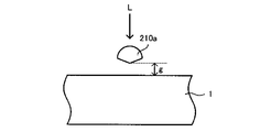
- FIG. 3 is a conceptual diagram showing a gap between the bottom of the SIL and the optical disc surface according to this embodiment.
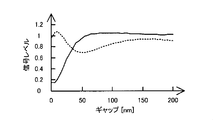
- FIG. 4 is an example of a simulation result showing the relationship between the signal level of each of the GE signal and the RF signal and the gap for each numerical aperture of the SIL. The simulation is performed on the assumption that the optical disk 1 has no irregularities such as marks (that is, as a flat plate).
- 4A, 4B, 4C, and 4D are examples of simulation results when the numerical aperture of the SIL 210a is 1.5, 1.8, 2.0, and 2.26, respectively. is there.
- the solid line indicates the GE signal
- the dotted line indicates the RF signal.
- the vertical axis in FIGS. 4A to 4D represents the relative value when the signal level of the GE signal is 1 when the gap is infinite.
- the GE signal is caused by the light reflected from the bottom surface of the SIL 210a. For this reason, when the gap g shown in FIG. 3 is reduced and evanescent light is emitted, the light reflected from the bottom surface of the SIL 210a is reduced and the signal level of the GE signal is lowered. Therefore, it is shown that the light contributing to the reproduction of the information recorded on the optical disc 1 increases as the signal level of the GE signal approaches zero.
- the signal level of the GE signal is zero when the gap g is near zero.
- the signal level of the GE signal may not be zero if any physical quantity or parameter related to reproduction characteristics such as jitter is within an allowable range. This is caused by a phenomenon peculiar to evanescent light generated between the SIL 210a and the optical disc 1.
- the signal level of the GE signal is close to zero when the gap g is close to zero.
- the signal level of the GE signal is set. It can be seen that it can approach zero.
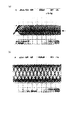
- FIG. 5A is an oscilloscope image showing an example of the RF signal
- FIG. 5B is an oscilloscope image showing an example of the RF signal processed by the equalizer.
- the track pitch of the optical disc 1 is 160 nm
- the shortest mark length (here, the mark length corresponding to 2T) is 75 nm.
- the numerical aperture of the SIL 210a included in the recording / reproducing apparatus is 2.0.
- a rhombus formed by overlapping the waveforms of the RF signals can be clearly observed. If sufficient light does not contribute to the reproduction of information recorded on the optical disc 1, the rhombus resulting from the RF signal processed by the equalizer may be blurred or the rhombus may not be observed. It has been found by research.
- an optical disc having a capacity of at least 100 GB can be realized.
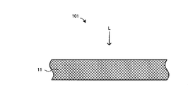
- FIG. 6 is a schematic cross-sectional view of an optical disc according to a comparative example of the present embodiment having the same purpose as FIG.
- an optical disk 101 is configured to include a substrate 11 made of polycarbonate.
- the refractive index of the substrate 11 is 1.55.
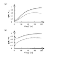
- FIG. 7 is an example of a simulation result showing the relationship between the signal level of each of the GE signal and the RF signal and the gap for each numerical aperture of the SIL, which has the same meaning as in FIG.
- FIG. 7A and 7B are examples of simulation results when the numerical aperture of the SIL 210a is 1.5 and 2.0, respectively.
- the solid line indicates the GE signal
- the dotted line indicates the RF signal.
- FIG. 8 is an example of a simulation result showing the relationship between the signal level of each of the GE signal and the RF signal and the gap having the same meaning as in FIG.
- the numerical aperture of the SIL 210a is 2.0. Further, the solid line in the figure indicates the GE signal, and the dotted line indicates the RF signal.
- the configuration of the optical disc according to the first modification of the present embodiment is the same as the configuration of the optical disc 1 according to the present embodiment shown in FIG. 1, but the film thickness of the dielectric film 13 is 55 nm. Note that the thickness of each of the reflective film 12 and the protective film 14 is the same as that of the optical disc 1 according to this embodiment.
- the optical disc according to the present modification it is possible to realize a high recording density of the optical disc.
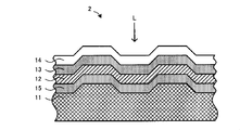
- FIG. 9 is a schematic cross-sectional view of an optical disc according to a second modification of the present embodiment having the same meaning as in FIG.
- the optical disc 2 includes a substrate 11, a reflective film 12, dielectric films 13 and 15, and a protective film 14.
- the “dielectric film 15” according to the present embodiment is an example of the “fourth laminated film” according to the present invention.
- FIG. 10 is a schematic cross-sectional view of an optical disc according to a third modification of the present embodiment having the same meaning as in FIG.
- the optical disk 3 includes a substrate 11, a reflective film 12, a dielectric film 13, a protective film 14, and a corrosion-resistant film 16.
- the “corrosion resistant film 16” according to the present embodiment is another example of the “fourth laminated film” according to the present invention.
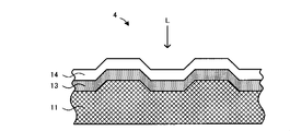
- FIG. 11 is a schematic cross-sectional view of the optical disc according to this embodiment having the same purpose as FIG.
- the optical disk 4 includes a substrate 11, a dielectric film 13, and a protective film 14.
- the film thickness of the dielectric film 13 is 55 nm
- the film thickness of the protective film 14 is 20 nm.
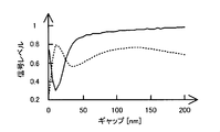
- FIG. 12 is an example of a simulation result showing the relationship between the signal level of each of the GE signal and the RF signal and the gap having the same meaning as in FIG.
- the numerical aperture of the SIL 210a is 2.0. Further, the solid line in the figure indicates the GE signal, and the dotted line indicates the RF signal.
- the optical disc according to the present embodiment it is possible to realize a high recording density of the optical disc.
- the signal level of the GE signal is about 0.75, but when recording information on the optical disk or reproducing information recorded on the optical disk, For example, since the gap is set in the range of 10 nm to 25 nm, there is no practical problem.
- FIG. 13 is a schematic cross-sectional view of the optical disc according to this embodiment having the same purpose as FIG.
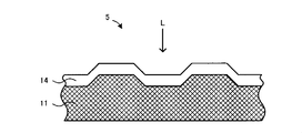
- the optical disk 5 includes a substrate 11 and a protective film 14.
- the protective film 14 has a thickness of 75 nm.
- FIG. 14 is an example of a simulation result showing the relationship between the signal level and the gap of each of the GE signal and the RF signal, which has the same concept as in FIG.
- the numerical aperture of the SIL 210a is 2.0.
- the solid line in the figure indicates the GE signal, and the dotted line indicates the RF signal.
- the optical disc according to the present embodiment it is possible to realize a high recording density of the optical disc.
Landscapes
- Physics & Mathematics (AREA)
- Optics & Photonics (AREA)
- Optical Record Carriers And Manufacture Thereof (AREA)
Abstract
光ディスク(1)は、ソリッドイマージョンレンズ(210a)を備える記録再生装置において、情報の記録又は再生が行われる光ディスクである。該光ディスクは、基板(11)と、基板の一の基板面上に夫々積層された第1積層膜(13)及び第2積層膜(14)とを備える。ソリッドイマージョンレンズの開口数をNAとし、基板の屈折率をnsとし、第1積層膜の屈折率をn1とし、第2積層膜の屈折率をn2としたときに、基板、第1積層膜及び第2積層膜を構成する材料は、n1>NA>n2>nsを満足するように設定される。
Description
本発明は、例えばエバネッセント光を介した情報の記録又は再生に用いられる光ディスクの技術分野に関する。
この種の光ディスクとして、例えば、光照射側の最表面に記録部を設けた光記録媒体が提案されている。ここでは特に、記録部の屈折率をnとし、集光レンズの開口数をNAとするとき、n≧NAの関係であることが開示されている(特許文献1参照)。
或いは、基板上に記録膜及び透明誘電体層を備える光記録媒体が提案されている。ここでは特に、透明誘電体層を、平均屈折率が1.4~2の材料を用いて構成すると共に、膜厚を厚くすることによって、記録時の光記録媒体の温度上昇を抑制する技術が開示されている(特許文献2参照)。
或いは、基板上に記録膜及び透明誘電体層を備える光記録媒体が提案されている。ここでは特に、イマージョンレンズの屈折率と透明誘電体層の平均屈折率との差を0~0.05とすることによって、記録時の光記録媒体の温度上昇を抑制する技術が開示されている(特許文献3参照)。
或いは、信号記録層の上層側に、複数の無反射コーティング層を備える情報記録ディスクが提案されている(特許文献4参照)。
しかしながら、特許文献1に記載の技術では、高記録密度化を十分には達成することが困難であるという技術的問題点がある。また、特許文献2乃至4に記載の技術では、上記問題点を解決することは極めて困難であるという技術的問題点ある。
本発明は、例えば上記問題点に鑑みてなされたものであり、高記録密度化を実現することができる光ディスクを提供することを課題とする。
本発明の光ディスクは、上記課題を解決するために、ソリッドイマージョンレンズを備える記録再生装置において、情報の記録又は再生が行われる光ディスクであって、基板と、前記基板の一の基板面上に夫々積層された第1及び第2積層膜とを備え、前記ソリッドイマージョンレンズの開口数をNAとし、前記基板の屈折率をnsとし、前記第1積層膜の屈折率をn1とし、前記第2積層膜の屈折率をn2としたときに、下記の式、n1>NA>n2>nsを満足するように設定される。
本発明の光ディスクによれば、当該光ディスクは、ソリッドイマージョンレンズ(Solid Immersion Lens:SIL)を備える記録再生装置において、情報の記録又は再生が行われる。尚、情報は、光ディスクの記録面に形成された複数のマーク及び複数のスペースの配列として記録される。
光ディスクは、例えばポリカーボネート等を含む基板と、該基板の一の基板面上に積層され、例えばZnS-SiO2等を含む第1積層膜と、一の基板面上に積層され、例えばSiN等を含む第2積層膜とを備えている。ここに、本発明に係る「一の基板面」とは、典型的には、基板の、記録再生装置から当該光ディスクに照射される光が入射する側の面を意味する。
尚、第1積層膜及び第2積層膜は、どちらが上層側に積層されていてもよい。即ち、第2積層膜の上層側に第1積層膜が積層されていてもよいし、第1積層膜の上層側に第2積層膜が積層されていてもよい。
ソリッドイマージョンレンズの開口数をNAとし、基板の屈折率をnsとし、第1積層膜の屈折率をn1とし、第2積層膜の屈折率をn2としたときに、基板、第1積層膜及び第2積層膜を構成する材料は、n1>NA>n2>nsを満足するように設定される。尚、基板の屈折率は、1以上であることが望ましい。
本願発明者の研究によれば、実効開口数が1.0を超えるソリッドイマージョンレンズを備える記録再生装置において、光ディスクに記録された情報を読み取る(即ち、再生する)場合、ソリッドイマージョンレンズの開口数を増加させたとしても、光ディスクの基板を構成する材料の屈折率以上の開口数の光が情報の再生に寄与せず、光ディスクの高記録密度化の妨げになっていることが判明している。
尚、「光ディスクの基板を構成する材料の屈折率以上の開口数の光」とは、基板を構成する材料の屈折率の値と等しい値を有する開口数に対応する最大錐角以上、ソリッドイマージョンレンズの開口数に対応する最大錐角以下の範囲に含まれる光を意味する。具体的には例えば、基板を構成する材料の屈折率を1.5とし、ソリッドイマージョンレンズの開口数を2.0とすると、開口数1.5に対応する最大錐角以上、開口数2.0に対応する最大錐角以下の範囲に含まれる光を意味する。
本願発明者の研究によれば、更に、光ディスクの基板上に、ソリッドイマージョンレンズの開口数より大きな値を有する屈折率の材料からなる積層膜を積層すれば、理論的には、記録密度を向上させることが可能である。しかしながら、例えばジッタ等の影響により実用可能な記録密度は制限されてしまうことが判明している。
しかるに本発明では、一の基板面上に、n1>NAの関係を満足する屈折率を有する第1積層膜と、NA>n2>nsの関係を満足する屈折率を有する第2積層膜とが積層されている。このため、第1積層膜により、理論的な記録密度の上限値を向上させることができ、更に、複数の積層膜を一の基板面上に積層することにより、例えばジッタ等を抑制して実用可能な記録密度の上限値を向上させることができる。
以上の結果、本発明の光ディスクによれば、光ディスクの高記録密度化を実現することができる。加えて、基板を構成する材料の屈折率は制限されないため、基板を構成する材料の自由度を増加させることができ、実用上非常に有利である。具体的には例えば、基板を構成する材料をポリカーボネートとすれば、比較的容易にして、射出成型により大量複製が可能となる。
本発明の光ディスクの一態様では、前記第2積層膜は、前記第1積層膜の上層側に積層されている。
この態様によれば、第2積層膜に、例えば保護膜としての機能を持たせることができる。この結果、別途保護膜を設ける必要がなく、例えば製造コスト等を抑制することができ、実用上非常に有利である。
本発明の光ディスクの他の態様では、前記一の基板面上に積層され、光を吸収する材料を含んでなる第3積層膜を更に備える。
この態様によれば、当該光ディスクは、例えば金属等の光を吸収する材料を含んでなる第3積層膜を更に備えている。ここに、本発明に係る「光を吸収する材料」とは、吸光係数の比較的大きい材料を意味する。
尚、第3積層膜は、第1積層膜及び第2積層膜の上層側に積層されてもよいし、下層側に積層されてもよい。或いは、第1積層膜及び第2積層膜の層間に積層されてもよい。また、第3積層膜の屈折率に制限は設けられていない。
本願発明者の研究によれば、第3積層膜の屈折率が、仮に基板の屈折率よりも小さくても、吸光係数が比較的大きければ(典型的には、屈折率と吸光係数とにより定義される複素屈折率の絶対値が、ソリッドイマージョンレンズの開口数の値よりも大きければ)、光ディスクの記録密度を向上させることができることが判明している。
従って、この態様によれば、光ディスクの記録密度をより向上させることができる。
この第3積層膜を備える態様では、前記第1積層膜は、前記第3積層膜の上層側に積層され、前記第2積層膜は、前記第1積層膜の上層側に積層されていてよい。
このように構成すれば、第3積層膜に、例えば反射膜としての機能を持たせることができると共に、第2積層膜に、例えば保護膜としての機能を持たせることができる。
この第3積層膜を備える態様では、前記一の基板面上に積層された第4積層膜を更に備えてよい。
このように構成すれば、例えばジッタ等をより抑制することができ、実用上非常に有利である。
この第4積層膜を備える態様では、前記第4積層膜は、前記第3積層膜の下層側に積層されていてよい。
このように構成すれば、第4積層膜を、例えば耐食性層として機能させることができる。この結果、当該光ディスクに記録された情報の劣化を抑制することができ、実用上非常に有利である。
尚、第4積層膜の屈折率は、第1積層膜の屈折率と同じであってもよいし、第2積層膜の屈折率と同じであってもよい。
本発明の光ディスクの他の態様では、前記開口数は1.0より大きい。
この態様によれば、光ディスクの記録密度を向上させることができ、実用上非常に有利である。
本発明の光ディスクの他の態様では、前記第1積層膜の膜厚は5nm(ナノメートル)より厚い。
この態様によれば、光ディスクの基板を構成する材料の屈折率以上の開口数の光を情報の再生に、確実に寄与させることができる。尚、第1積層膜の膜厚の上限値は、100nm程度であることが望ましい。
第3積層膜を備える態様では、前記第3積層膜の膜厚は5nmより厚くてよい。
このように構成すれば、第3積層膜を構成する材料の吸光係数に起因する光ディスクの記録密度を向上させるという効果を確実に得ることができる。
第3積層膜を備える態様では、前記第1積層膜の膜厚及び前記第3積層膜の膜厚の合計は、5nmより厚くてよい。
このように構成すれば、光ディスクの記録密度を向上させるという効果を確実に得ることができる。
本発明の作用及び他の利得は次に説明する実施するための最良の形態から明らかにされよう。
1~5、101 光ディスク
11 基板
12 反射膜
13、15 誘電体膜
14 保護膜
16 耐食性膜
200 光ピックアップ
11 基板
12 反射膜
13、15 誘電体膜
14 保護膜
16 耐食性膜
200 光ピックアップ
以下、本発明の光ディスクに係る実施形態を図面に基づいて説明する。
<第1実施形態>
本発明の光ディスクに係る第1実施形態を、図1乃至図5を参照して説明する。
本発明の光ディスクに係る第1実施形態を、図1乃至図5を参照して説明する。
先ず、図1を参照して本実施形態に係る光ディスク1の構成について説明する。図1は、本実施形態に係る光ディスクの断面模式図である。
図1において、光ディスク1は、基板11、反射膜12、誘電体膜13及び保護膜14を備えて構成されている。ここに、本実施形態に係る「反射膜12」、「誘電体膜13」及び「保護膜14」は、夫々、本発明に係る「第3積層膜」、「第1積層膜」及び「第2積層膜」の一例である。また、本実施形態に係る「基板11の光Lが入射する側の面(即ち、図1における基板11の上面)」は、本発明に係る「一の基板面」の一例である。
ここで、基板11はポリカーボネートからなり、その屈折率は1.55である。反射膜12は、例えばAgPdCu等の銀合金(Ag alloy)からなり、その屈折率は0.8、吸光係数は2.5、膜厚は25nmである。誘電体膜13はZnS-SiO2からなり、その屈折率は2.3、膜厚は20nmである。保護膜14はSiNからなり、その屈折率は1.8、膜厚は20nmである。尚、基板11、反射膜12、誘電体膜13及び保護膜14各々を構成する材料や膜厚等は、上述の材料等に限られない。
次に、光ディスク1に情報の記録を行う、或いは、光ディスク1に記録された情報の再生を行う、ソリッドイマージョンレンズ(以下、適宜“SIL”と称する)を備える記録再生装置について、図2を参照して説明する。ここに、図2は、本実施形態に係る記録再生装置の光ピックアップにおける光路を示す光路図である。尚、図中の点線Lは光路を示している。
図2において、光ピックアップ200は、半導体レーザ201、コリメータレンズ202、アナモフィックプリズム203、回折格子204、無偏光ビームスプリッタ205、偏光ビームスプリッタ206、ビーム拡大器207、4分の1波長板208、ミラー209、SIL210aを有するSILアセンブリ210、レンズ211及び213、RF(Radio Frequency)用受光素子212、GE(Gap Error)用受光素子214並びにフロントモニタ(FM)215を備えて構成されている。
尚、RF用受光素子212は、2又は4分割受光素子である。他方、GE用受光素子214は、分割型受光素子であってもよいし、分割されてない受光素子であってもよい。
半導体レーザ201から出射された光Lは、コリメータレンズ202及びアナモフィックプリズム203を介して、回折格子204に入射する。該回折格子204によって複数の回折光に分離された光Lは、無偏光ビームスプリッタ205、偏光ビームスプリッタ206、ビーム拡大器207、4分の1波長板208及びミラー209を介して、SILアセンブリ210に入射する。
尚、無偏光ビームスプリッタ205に入射した光Lの一部は、フロントモニタ215によって受光される。該フロントモニタ215には、図示しないパワー比較回路が電気的に接続されている。該パワー比較回路では、典型的には、フロントモニタ215から送信された光Lの強度を示す信号と基準信号とが比較され、その結果を示す信号に基づいて半導体レーザ201の出力が制御される。
SIL210aに入射した光Lの一部は、エバネッセント光として光ディスク1に出射され、他の一部はSIL210aの底部で反射される。光ディスク1からの反射光は、再びSIL210aに入射し、ミラー209、4分の1波長板208及びビーム拡大器207を介して、偏光ビームスプリッタ206に入射する。ここで、半導体レーザ201から出射される光Lの偏光方向と、光ディスク1からの反射光の偏光方向とは90度異なっているため、光ディスク1からの反射光は、レンズ211を介して、RF用受光素子212に入射する。
尚、RF用受光素子212には、図示しないRF信号生成回路が電気的に接続されており、RF用受光素子212に入射した反射光に起因するRF信号が生成される。該生成されたRF信号は、図示しない、例えば復調回路、エラー訂正回路、デコード回路等を含んで構成される再生信号処理部に送信される。或いは、図示しないトラッキングサーボ回路に送信される。該トラッキングサーボ回路によってトラッキングエラー信号が生成され、該生成されたトラッキングエラー信号に基づいて、光ディスク1上のスポットの位置が所定の位置となるように、図示しないレンズアクチュエータが制御される。
他方、SIL210aの底部で反射した光は、ミラー209、4分の1波長板208、ビーム拡大器207及び偏光ビームスプリッタ206を介して、無偏光ビームスプリッタ205に入射する。SIL210aの底部で反射した光の一部は、レンズ213を介して、GE用受光素子214に入射する。
尚、GE用受光素子214には、図示しないGE信号生成回路が電気的に接続されており、GE用受光素子214に入射した光に起因するGE信号が生成される。該生成されたGE信号は、図示しないギャップエラーサーボ回路に送信される。該ギャップエラーサーボ回路では、典型的には、送信されたGE信号と基準信号とが比較され、その結果を示す信号に基づいて、SIL210aの底部及び光ディスク1の表面間の距離(即ち、図3におけるギャップg)が所定距離となるように、図示しないレンズアクチュエータが制御される。ここに、図3は、本実施形態に係るSILの底部及び光ディスク表面間のギャップを示す概念図である。
次に、上述の如く構成された記録再生装置において、光ディスク1に光Lを照射した際に得られるGE信号及びRF信号各々の信号レベルとギャップとの関係を、図4を参照して説明する。ここに、図4は、GE信号及びRF信号各々の信号レベルとギャップとの関係を、SILの開口数毎に示す、シミュレーション結果の一例である。尚、シミュレーションは、光ディスク1にマーク等の凹凸がないものとして(即ち、平板として)行っている。
図4(a)、(b)、(c)及び(d)は、夫々、SIL210aの開口数が1.5、1.8、2.0及び2.26である場合のシミュレーション結果の一例である。尚、図中の実線がGE信号を示しており、点線がRF信号を示している。また、図4(a)乃至(d)における縦軸は、ギャップが無限遠である場合のGE信号の信号レベルを1としたときの相対値を示している。
上述の如く、GE信号は、SIL210aの底面で反射した光に起因している。このため、図3に示したギャップgが小さくなりエバネッセント光が出射されると、SIL210aの底面で反射する光が少なくなりGE信号の信号レベルが低下する。従って、GE信号の信号レベルがゼロに近づくほど、光ディスク1に記録された情報の再生に寄与する光が多くなることを示している。
尚、ギャップgがゼロ近傍であるときに、GE信号の信号レベルがゼロであることが望ましい。しかしながら、実用上は、例えばジッタ等の再生特性に係る何らかの物理量又はパラメータが許容範囲内であれば、GE信号の信号レベルがゼロでなくてもよい。これは、SIL210a及び光ディスク1間において生じるエバネッセント光に特有の現象に起因している。
図4(a)乃至(d)に示すように、SIL210aの開口数がいずれの場合であっても、ギャップgがゼロ近傍であるときに、GE信号の信号レベルがゼロ近傍となっている。ここでは特に、光ディスク1を図1のように構成することにより、基板11の屈折率である1.55より大きい値の開口数を有するSIL210aを用いた場合であってもGE信号の信号レベルをゼロに近づけることができることがわかる。
次に、100GB(ギガバイト)の容量を有するように、トラックピッチやマーク長等が設定された光ディスク1に記録された情報を再生する際に得られるRF信号について、図5を参照して説明する。ここに、図5(a)は、RF信号の一例を示すオシロスコープ画像であり、図5(b)は、イコライザで処理されたRF信号の一例を示すオシロスコープ画像である。
尚、光ディスク1のトラックピッチは160nmであり、最短マーク長(ここでは、2Tに対応するマーク長)は75nmである。また、記録再生装置が備えるSIL210aの開口数は、2.0である。
図5(a)に示すように、ジッタが比較的少ない(ここでは、6.8%)ので、RF信号の波形を鮮明に観測することができる。尚、図5(a)中に矢印で示す、比較的色の濃い部分(即ち、RF信号の振幅方向の中心近傍)は、最短マークである2Tに対応するRF信号である。
また、図5(b)に示すように、イコライザで処理された後のRF信号では、RF信号の波形が相互に重なることによってできる菱形を鮮明に観測することができる。仮に、十分な光が光ディスク1に記録された情報の再生に寄与しなければ、イコライザで処理されたRF信号に起因する菱形が不鮮明になる、或いは菱形が観測されなくなることが、本願発明者の研究により判明している。
以上の結果、本実施形態に係る光ディスク1によれば、少なくとも100GBの容量を有する光ディスクを実現することができる。
(比較例)
次に、本実施形態に係る光ディスクの比較例について、図6及び図7を参照して説明する。ここに、図6は、図1と同趣旨の、本実施形態の比較例に係る光ディスクの断面模式図である。
次に、本実施形態に係る光ディスクの比較例について、図6及び図7を参照して説明する。ここに、図6は、図1と同趣旨の、本実施形態の比較例に係る光ディスクの断面模式図である。
図6において、光ディスク101は、ポリカーボネートからなる基板11を備えて構成されている。尚、基板11の屈折率は1.55である。
次に、上述の如く構成された光ディスク101に光Lを照射した際に得られるGE信号及びRF信号各々の信号レベルとギャップとの関係を、図7を参照して説明する。ここに、図7は、図4と同趣旨の、GE信号及びRF信号各々の信号レベルとギャップとの関係を、SILの開口数毎に示す、シミュレーション結果の一例である。
図7(a)及び(b)は、夫々、SIL210aの開口数が1.5及び2.0である場合のシミュレーション結果の一例である。尚、図中の実線がGE信号を示しており、点線がRF信号を示している。
図7(a)に示すように、SIL210aの開口数の値(即ち、1.5)が基板11の屈折率(即ち、1.55)よりも小さければ、ギャップがゼロ近傍であるときに、GE信号の信号レベルがゼロ近傍となっている。他方、図7(b)に示すように、SIL210aの開口数の値(即ち、2.0)が基板11の屈折率よりも大きい場合、GE信号の信号レベルは、ゼロ近傍まで低下していない。これは、基板11の屈折率以上の開口数の光が、SIL210aの底面で反射してしまうことに起因している。
(第1変形例)
次に、本実施形態に係る光ディスクの第1変形例について、図8を参照して説明する。ここに、図8は、図4と同趣旨の、GE信号及びRF信号各々の信号レベルとギャップとの関係を示すシミュレーション結果の一例である。尚、SIL210aの開口数は、2.0である。また、図中の実線がGE信号を示しており、点線がRF信号を示している。
次に、本実施形態に係る光ディスクの第1変形例について、図8を参照して説明する。ここに、図8は、図4と同趣旨の、GE信号及びRF信号各々の信号レベルとギャップとの関係を示すシミュレーション結果の一例である。尚、SIL210aの開口数は、2.0である。また、図中の実線がGE信号を示しており、点線がRF信号を示している。
ここで、本実施形態の第1変形例に係る光ディスクの構成は、図1に示した本実施形態に係る光ディスク1の構成と同様であるが、誘電体膜13の膜厚が55nmである。尚、反射膜12及び保護膜14各々の膜厚は、本実施形態に係る光ディスク1と同じである。
図8に示すように、ギャップがゼロ近傍であるときに、GE信号の信号レベルがゼロ近傍となっている。従って、本変形例に係る光ディスクによれば、光ディスクの高記録密度化を実現することができる。
(第2変形例)
次に、本実施形態に係る光ディスクの第2変形例について、図9を参照して説明する。ここに、図9は、図1と同趣旨の、本実施形態の第2変形例に係る光ディスクの断面模式図である。
次に、本実施形態に係る光ディスクの第2変形例について、図9を参照して説明する。ここに、図9は、図1と同趣旨の、本実施形態の第2変形例に係る光ディスクの断面模式図である。
図9において、光ディスク2は、基板11、反射膜12、誘電体膜13及び15、並びに保護膜14を備えて構成されている。ここに、本実施形態に係る「誘電体膜15」は、本発明に係る「第4積層膜」の一例である。
(第3変形例)
次に、本実施形態に係る光ディスクの第3変形例について、図10を参照して説明する。ここに、図10は、図1と同趣旨の、本実施形態の第3変形例に係る光ディスクの断面模式図である。
次に、本実施形態に係る光ディスクの第3変形例について、図10を参照して説明する。ここに、図10は、図1と同趣旨の、本実施形態の第3変形例に係る光ディスクの断面模式図である。
図9において、光ディスク3は、基板11、反射膜12、誘電体膜13、保護膜14及び耐食性膜16を備えて構成されている。ここに、本実施形態に係る「耐食性膜16」は、本発明に係る「第4積層膜」の他の例である。
<第2実施形態>
次に、本発明の光ディスクに係る第2実施形態を、図11及び図12を参照して説明する。第2実施形態では、反射膜を備えていない点が異なる以外は、第1実施形態と同様である。よって、第2実施形態について、第1実施形態と重複する説明を省略すると共に、図面上における共通箇所には同一符号を付して示し、基本的に異なる点についてのみ、図11及び図12を参照して説明する。ここに、図11は、図1と同趣旨の、本実施形態に係る光ディスクの断面模式図である。
次に、本発明の光ディスクに係る第2実施形態を、図11及び図12を参照して説明する。第2実施形態では、反射膜を備えていない点が異なる以外は、第1実施形態と同様である。よって、第2実施形態について、第1実施形態と重複する説明を省略すると共に、図面上における共通箇所には同一符号を付して示し、基本的に異なる点についてのみ、図11及び図12を参照して説明する。ここに、図11は、図1と同趣旨の、本実施形態に係る光ディスクの断面模式図である。
図11において、光ディスク4は、基板11、誘電体膜13及び保護膜14を備えて構成されている。尚、誘電体膜13の膜厚は55nmであり、保護膜14の膜厚は20nmである。
次に、上述の如く構成された光ディスク4に光Lを照射した際に得られるGE信号及びRF信号各々の信号レベルとギャップとの関係を、図12を参照して説明する。ここに、図12は、図4と同趣旨の、GE信号及びRF信号各々の信号レベルとギャップとの関係を示すシミュレーション結果の一例である。尚、SIL210aの開口数は、2.0である。また、図中の実線がGE信号を示しており、点線がRF信号を示している。
図12に示すように、ギャップがゼロ近傍であるときに、GE信号の信号レベルがゼロ近傍となっている。従って、本実施形態に係る光ディスクによれば、光ディスクの高記録密度化を実現することができる。
尚、図12において、ギャップがゼロのときに、GE信号の信号レベルが約0.75となっているが、光ディスクに情報を記録する際、或いは光ディスクに記録された情報を再生する際は、例えば10nm~25nmの範囲にギャップが設定されるので、実用上何らの問題もない。
<第3実施形態>
次に、本発明の光ディスクに係る第3実施形態を、図13及び図14を参照して説明する。第3実施形態では、反射膜及び誘電体膜を備えていない点が異なる以外は、第1実施形態と同様である。よって、第3実施形態について、第1実施形態と重複する説明を省略すると共に、図面上における共通箇所には同一符号を付して示し、基本的に異なる点についてのみ、図13及び図14を参照して説明する。ここに、図13は、図1と同趣旨の、本実施形態に係る光ディスクの断面模式図である。
次に、本発明の光ディスクに係る第3実施形態を、図13及び図14を参照して説明する。第3実施形態では、反射膜及び誘電体膜を備えていない点が異なる以外は、第1実施形態と同様である。よって、第3実施形態について、第1実施形態と重複する説明を省略すると共に、図面上における共通箇所には同一符号を付して示し、基本的に異なる点についてのみ、図13及び図14を参照して説明する。ここに、図13は、図1と同趣旨の、本実施形態に係る光ディスクの断面模式図である。
図13において、光ディスク5は、基板11及び保護膜14を備えて構成されている。尚、保護膜14の膜厚は75nmである。
次に、上述の如く構成された光ディスク5に光Lを照射した際に得られるGE信号及びRF信号各々の信号レベルとギャップとの関係を、図14を参照して説明する。ここに、図14は、図4と同趣旨の、GE信号及びRF信号各々の信号レベルとギャップとの関係を示すシミュレーション結果の一例である。尚、SIL210aの開口数は、2.0である。また、図中の実線がGE信号を示しており、点線がRF信号を示している。
図14に示すように、ギャップがゼロ近傍であるときに、GE信号の信号レベルがゼロ付近となっている。従って、本実施形態に係る光ディスクによれば、光ディスクの高記録密度化を実現することができる。
尚、本発明は、上述した実施形態に限られるものではなく、請求の範囲及び明細書全体から読み取れる発明の要旨、或いは思想に反しない範囲で適宜変更可能であり、そのような変更を伴う光ディスクもまた、本発明の技術的範囲に含まれるものである。
Claims (10)
- ソリッドイマージョンレンズを備える記録再生装置において、情報の記録又は再生が行われる光ディスクであって、
基板と、
前記基板の一の基板面上に夫々積層された第1及び第2積層膜と
を備え、
前記ソリッドイマージョンレンズの開口数をNAとし、前記基板の屈折率をnsとし、前記第1積層膜の屈折率をn1とし、前記第2積層膜の屈折率をn2としたときに、下記の式、
n1>NA>n2>ns
を満足するように設定される
ことを特徴とする光ディスク。 - 前記第2積層膜は、前記第1積層膜の上層側に積層されていることを特徴とする請求の範囲第1項に記載の光ディスク。
- 前記一の基板面上に積層され、光を吸収する材料を含んでなる第3積層膜を更に備えることを特徴とする請求の範囲第1項に記載の光ディスク。
- 前記第1積層膜は、前記第3積層膜の上層側に積層され、
前記第2積層膜は、前記第1積層膜の上層側に積層されている
ことを特徴とする請求の範囲第3項に記載の光ディスク。 - 前記一の基板面上に積層された第4積層膜を更に備えることを特徴とする請求の範囲第3項に記載の光ディスク。
- 前記第4積層膜は、前記第3積層膜の下層側に積層されていることを特徴とする請求の範囲第5項に記載の光ディスク。
- 前記開口数は1.0より大きいことを特徴とする請求の範囲第1項に記載の光ディスク。
- 前記第1積層膜の膜厚は5nmより厚いことを特徴とする請求の範囲第1項に記載の光ディスク。
- 前記第3積層膜の膜厚は5nmより厚いことを特徴とする請求の範囲第3項に記載の光ディスク。
- 前記第1積層膜の膜厚及び前記第3積層膜の膜厚の合計は、5nmより厚いことを特徴とする請求の範囲第3項に記載の光ディスク。
Priority Applications (1)
| Application Number | Priority Date | Filing Date | Title |
|---|---|---|---|
| PCT/JP2008/062594 WO2010004648A1 (ja) | 2008-07-11 | 2008-07-11 | 光ディスク |
Applications Claiming Priority (1)
| Application Number | Priority Date | Filing Date | Title |
|---|---|---|---|
| PCT/JP2008/062594 WO2010004648A1 (ja) | 2008-07-11 | 2008-07-11 | 光ディスク |
Publications (1)
| Publication Number | Publication Date |
|---|---|
| WO2010004648A1 true WO2010004648A1 (ja) | 2010-01-14 |
Family
ID=41506779
Family Applications (1)
| Application Number | Title | Priority Date | Filing Date |
|---|---|---|---|
| PCT/JP2008/062594 Ceased WO2010004648A1 (ja) | 2008-07-11 | 2008-07-11 | 光ディスク |
Country Status (1)
| Country | Link |
|---|---|
| WO (1) | WO2010004648A1 (ja) |
Cited By (1)
| Publication number | Priority date | Publication date | Assignee | Title |
|---|---|---|---|---|
| JP5441902B2 (ja) * | 2008-06-13 | 2014-03-12 | パナソニック株式会社 | 情報記録媒体とそれを用いた記録再生方法 |
Citations (3)
| Publication number | Priority date | Publication date | Assignee | Title |
|---|---|---|---|---|
| JP2002050043A (ja) * | 2000-05-26 | 2002-02-15 | Tosoh Corp | 表面再生型光記録媒体 |
| JP2002163842A (ja) * | 2000-11-21 | 2002-06-07 | Tosoh Corp | 表面再生型光記録媒体 |
| JP2002260279A (ja) * | 2001-03-05 | 2002-09-13 | Tosoh Corp | 光記録媒体 |
-
2008
- 2008-07-11 WO PCT/JP2008/062594 patent/WO2010004648A1/ja not_active Ceased
Patent Citations (3)
| Publication number | Priority date | Publication date | Assignee | Title |
|---|---|---|---|---|
| JP2002050043A (ja) * | 2000-05-26 | 2002-02-15 | Tosoh Corp | 表面再生型光記録媒体 |
| JP2002163842A (ja) * | 2000-11-21 | 2002-06-07 | Tosoh Corp | 表面再生型光記録媒体 |
| JP2002260279A (ja) * | 2001-03-05 | 2002-09-13 | Tosoh Corp | 光記録媒体 |
Cited By (1)
| Publication number | Priority date | Publication date | Assignee | Title |
|---|---|---|---|---|
| JP5441902B2 (ja) * | 2008-06-13 | 2014-03-12 | パナソニック株式会社 | 情報記録媒体とそれを用いた記録再生方法 |
Similar Documents
| Publication | Publication Date | Title |
|---|---|---|
| US5485452A (en) | Optical information recording medium | |
| TWI279790B (en) | Optical pickup | |
| EP0520619A1 (en) | Optical information recording medium | |
| WO2010013441A1 (ja) | 光情報記録媒体及び記録再生装置 | |
| WO2012014429A1 (ja) | 光情報記録媒体及び駆動装置 | |
| KR100199298B1 (ko) | 한면 판독형 2층식 광디스크 및 재생헤드 | |
| US6321028B1 (en) | Optical disk recording/reproduction apparatus for recording/reproducing information to/from optical disk of different standards | |
| Mitsumori et al. | Multilayer 500 Gbyte optical disk | |
| KR101143028B1 (ko) | 다층 광학 정보 기록 매체 | |
| US7813258B2 (en) | Optical information recording medium and optical information reproducing method | |
| CN101499294A (zh) | 光学拾取头装置 | |
| JPWO2006093054A1 (ja) | ホログラム記録媒体及びホログラム記録再生装置 | |
| WO2010004648A1 (ja) | 光ディスク | |
| US8315147B2 (en) | Multilayer optical recording medium having three or more recording layers with reduced interlayer crosstalk | |
| JP4341496B2 (ja) | 多層光情報記録媒体 | |
| JP3708320B2 (ja) | 光情報検出装置 | |
| JP2001307376A (ja) | 光記録媒体及びピックアップ装置 | |
| WO2011064992A1 (ja) | 光ピックアップ装置および光ディスク装置 | |
| CN101295520B (zh) | 光拾取装置 | |
| JP2007272980A (ja) | 光ピックアップ装置 | |
| JP3703451B2 (ja) | 光記録媒体及びその製造方法 | |
| JPWO2003088224A1 (ja) | 光学的情報記録再生の方法及び装置 | |
| JP4437806B2 (ja) | 光集積ユニットおよびそれを備えた光ピックアップ装置 | |
| JP3887384B2 (ja) | 光情報検出装置 | |
| JP2003281779A (ja) | 光学的情報記録媒体およびそれを用いる光学的情報記録再生装置 |
Legal Events
| Date | Code | Title | Description |
|---|---|---|---|
| 121 | Ep: the epo has been informed by wipo that ep was designated in this application |
Ref document number: 08778109 Country of ref document: EP Kind code of ref document: A1 |
|
| NENP | Non-entry into the national phase |
Ref country code: DE |
|
| 122 | Ep: pct application non-entry in european phase |
Ref document number: 08778109 Country of ref document: EP Kind code of ref document: A1 |
|
| NENP | Non-entry into the national phase |
Ref country code: JP |