WO2009150949A1 - フィルタ - Google Patents
フィルタ Download PDFInfo
- Publication number
- WO2009150949A1 WO2009150949A1 PCT/JP2009/059953 JP2009059953W WO2009150949A1 WO 2009150949 A1 WO2009150949 A1 WO 2009150949A1 JP 2009059953 W JP2009059953 W JP 2009059953W WO 2009150949 A1 WO2009150949 A1 WO 2009150949A1
- Authority
- WO
- WIPO (PCT)
- Prior art keywords
- filter
- pass
- scaling
- frequency
- low
- Prior art date
Links
Images


Classifications
-
- H—ELECTRICITY
- H03—ELECTRONIC CIRCUITRY
- H03H—IMPEDANCE NETWORKS, e.g. RESONANT CIRCUITS; RESONATORS
- H03H17/00—Networks using digital techniques
- H03H17/02—Frequency selective networks
- H03H17/06—Non-recursive filters
-
- H—ELECTRICITY
- H03—ELECTRONIC CIRCUITRY
- H03H—IMPEDANCE NETWORKS, e.g. RESONANT CIRCUITS; RESONATORS
- H03H17/00—Networks using digital techniques
- H03H17/02—Frequency selective networks
- H03H17/0223—Computation saving measures; Accelerating measures
- H03H17/0227—Measures concerning the coefficients
- H03H17/0229—Measures concerning the coefficients reducing the number of taps
Definitions
- the present invention relates to a filter, and more particularly, to an FIR (Finite Impulse Response) filter having a small number of taps and a steep attenuation characteristic.
- FIR Finite Impulse Response
- Non-Patent Document 1 describes the Remez method that is normally used as a conventional method.
- Non-Patent Document 2 describes a configuration method of a low-sensitivity linear phase FIR filter using a cascade configuration, and reduces the number of multipliers using the cascade configuration.
- Patent Document 1 describes an FIR filter for the purpose of making the delay of a filter output signal variable.
- FIR filters according to applications such as a filter for band separation in an acoustic signal and a filter for image noise removal have been studied.
- Non-Patent Document 3 discloses the design and implementation of a non-maximum decimation filter bank for a low aliasing multilevel FIR filter.
- Non-Patent Document 4 discloses a filter bank that realizes desired frequency characteristics with low aliasing noise.
- Non-Patent Document 5 discloses a method for realizing a completely reconstructed non-maximum decimation cosine modulation filter bank.
- Patent Document 2 discloses a filter bank and a filtering method that can efficiently realize a maximum thinning filter bank for a signal having a real value and a cosine modulation filter bank as a special case thereof.
- An object of the present invention is to provide a filter capable of obtaining predetermined characteristics with a small number of input taps, a delay circuit, and a multiplier, and improving responsiveness and cost. I will.
- Another object of the present invention is to provide a low-cost FIR filter having excellent noise removal characteristics.
- Another object of the present invention is to provide an FIR filter suitable for signal processing that does not generate jaggy or the like.
- the FIR filter can be used in various devices such as an acoustic device such as an amplifier, an image device for processing moving images and still images, a communication device such as a mobile phone, a control device, a computer, and a PC.
- the passband can be narrowed according to the scale value by frequency scaling of the basic filter, and further, the attenuation in the stopband can be increased to increase the number of zeros. It is in.
- the cascade connection of the scaling filters is to combine a low-pass type and a high-pass type scaling filter having a pass band width equal to or wider than a desired pass band width, and having a cutoff frequency. Is to ensure a desired value.
- the scaling filter is selected using the attenuation in the stop band as an evaluation value, the attenuation in the stop band is very large.
- Low-pass filter L p scaled to filter
- a high-pass basic filter that is a coefficient obtained by inverting the sign of every other filter coefficient q + 1 times (q is an integer of 0 or more) on the time axis or frequency axis
- a filter formed as in (z) is provided.
- each subscript is as follows.
- ⁇ p , ⁇ p power value (indicating that the same L p and H q are connected ⁇ p times and
- the basic configuration is a configuration that sequentially adds signals delayed by multiplying a discrete input of a finite interval by a coefficient.
- the scaling filter is configured by increasing or decreasing the number of delay elements in the basic configuration, and the scaling filters are cascaded.
- a filter is provided that outputs a signal.
- a low-pass / high-pass basic filter whose coefficient is the nodal value of an impulse response function composed of piecewise polynomials on a finite platform, and multiple scalings that scale the basic filter on the time axis or frequency axis
- a FIR filter characterized by combining filters to obtain desired characteristics, a center frequency, a cutoff frequency, a stopband frequency, a maximum stopband attenuation, and a sampling frequency are input, and a pass determined by the cutoff frequency and the center frequency
- the maximum order of scaling is determined from the frequency band width, and a scaling filter having an order smaller than the scaling order is sequentially selected, and the attenuation at the stopband frequency of the FIR filter to be obtained is selected to be equal to or less than the predetermined maximum attenuation.
- FIR filter characterized in that the configuration is provided.
- ⁇ P , ⁇ P power value (same L P, N1 or [1-H P, N2 ] are connected ⁇ P times, ⁇ P times.
- N1 N p ( 1)
- N2 N p (2)
- the number of stages of N1 H P ladder connection in N P (2): [1 -H p, N2] in L number P ladder connection P Indicates a filter whose frequency is scaled by (P + 1) times.
- the low-pass basic filter L 0 and the low-pass filter L M , the high-pass basic filter H 0 and the high-pass filter H M are cascaded as represented by the following equation:
- N k number of stages of ladder connection of H p in L pk
- Nk N 1 number of stages of ladder connection of L p in [1-H ql, Nl ] p k , q l : frequency (p k +1), respectively
- a filter scaled by (q l +1) times is shown.
- the low-pass filter and the high-pass filter are scaled by frequency scaling.
- a filter is selected so that the pass bandwidth is equal to or greater than a predetermined required width, and a low-pass type scaling filter that satisfies the required characteristics is selected using the selected scaling filter, and the selected low-pass filter is selected.
- a filter characterized by forming a passband characteristic of a filter by connecting a high-pass type scaling filter in a ladder shape to a bandpass type scaling filter is provided.
- a seventh solution of the present invention Based on a low-pass filter and a high-pass filter whose coefficients are the node values of the impulse response function represented by a finite piecewise polynomial, the low-pass filter and the high-pass filter are scaled by frequency scaling.
- a filter is selected so that the passband width is equal to or greater than a predetermined required width, and a high-pass type scaling filter that satisfies the required characteristics is selected using the selected scaling filter.
- a filter characterized by forming a passband characteristic of a filter by connecting a low-pass type scaling filter in a ladder form to a bandpass type scaling filter is provided.
- a basic filter with good steepness is configured by a scaled filter, so a low-pass filter, a high-pass filter, and a band-pass filter with excellent frequency separation and a small number of taps, delay circuits, and multipliers are realized. it can. Further, according to the present invention, since the attenuation in the stop band can be increased, a filter having excellent noise removal characteristics can be realized. Furthermore, according to the present invention, the number of taps (the number of multipliers) can be greatly reduced as compared with a conventional filter, so that a low-cost filter is possible.
- the block diagram of the filter of this Embodiment The block diagram of the scaled element filter in this Embodiment. Schematic explanatory drawing of the filter process of this Embodiment.
- the block diagram of the general filter of this Embodiment The figure which shows the conventional impulse response function waveform of this Embodiment.
- the figure which shows the impulse response waveform of this Embodiment Explanatory drawing of the discrete impulse response and filter coefficient value of this Embodiment.
- FIG. 6 is an explanatory diagram of discrete impulse responses and filter coefficient values of the basic high-pass filter according to the present embodiment.
- a circuit diagram of the filter G is shown.
- a circuit diagram of G pass is shown. It shows the expanded view of G pass, indicating the preceding portion of the G pass. It shows the expanded view of G pass, indicating the Koko portion of G pass.
- a circuit diagram of G stop is shown. It is a hardware block diagram regarding this Embodiment.
- the flowchart of a filter design procedure (low-pass filter) is shown.
- blocking characteristic by the cascade connection model G (f) of a product-sum module is shown. It is explanatory drawing of a low-pass filter specification.
- G pass and G stop is an explanatory view of the filter G.
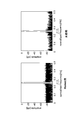
- the characteristic diagram of the filter comprised by the conventional method and this invention is shown.
- (A) is the least square method
- (b) is the Remez method
- (c) is the method according to the present invention. It is a figure which shows the number of multipliers in each design method, and the comparison of R. It is explanatory drawing of the example (low-pass filter) in which a characteristic is improved by G (f).
- FIG. 5 is a diagram showing a conventional impulse response function waveform.
- the SINC function shown in FIG. 5 is applied as the impulse response function, and the function value at a point half the sample interval is adopted as the filter coefficient C k .
- the SINC function is a function of an infinite interval, and an infinite number of filter coefficients C k are ideally required. In an actual filter, there must be a finite number of coefficients, but there is a problem that the number of coefficients must be very large in order to ensure error and accuracy due to the truncation of coefficients.
- FIG. 6 is a diagram showing an impulse response waveform of the present embodiment.
- a finite impulse response function as shown in FIG. 6 is used.
- this function there is the following function obtained by synthesizing by shifting the B-spline function every 1 ⁇ 2 interval between sample points.
- h sampling time interval
- f frequency
- FIG. 7 is an explanatory diagram of the discrete impulse response and the filter coefficient value of the present embodiment.
- the ⁇ marks in the figure indicate the sampling points (singular points) of the impulse response function of the finite platform.
- a function ⁇ (t) shown in the figure is given as an impulse response waveform of a finite stage, the delay time of the filter is set to 1 ⁇ 2 of the sampling time width h, and the value on the vertical axis marked with ⁇ is the filter coefficient (tap coefficient) ) If given to C (k), the lowest-order impulse response waveform is reproduced.
- the basic low-pass filter is expressed as follows.
- L 0 (z) L 0 (z) is as defined above. It becomes.
- the frequency characteristic of the basic low-pass filter is expressed by the following equation.
- FIG. 9 shows a configuration diagram of the basic low-pass filter of the present embodiment.
- the arithmetic circuit of the basic low-pass filter L 0 has a configuration shown in FIG. 9 as an example.
- This basic low-pass filter includes delay elements 91-1, 91-2, 91-3, 91-4, 91-5 and 91-6, multipliers 92-1, 92-2 and 92-3, and an adder. 93-1, 93-2, 93-3 and 93-4.
- the filter coefficients of the multipliers 92-1 to 92-3 are ⁇ 1/16, 9/16, and 1, respectively.
- the multiplier 92-3 can be omitted because the coefficient is 1.
- the basic high-pass filter H 0 (z) can be expressed by the following equation from the low-pass filter L 0 (z).
- FIG. 10 is an explanatory diagram of the discrete impulse response and filter coefficient values of the basic high-pass filter of the present embodiment.
- the coefficient b (k) in the above equation is a value obtained by alternately inverting the sign of the coefficient C (k) as shown in FIG.
- a filter scaled on the frequency axis is defined based on the basic low-pass filter L 0 (z) and the basic high-pass filter H 0 (z) described above. That is, a filter obtained by scaling the basic low-pass filter L 0 (z) and the basic high-pass filter H 0 (z) by (M + 1) times can be expressed by the following formulas, respectively, for the low-pass filter L M (z) and the high-pass filter H M (z). .
- FIG. 12 is an explanatory diagram of M-times scaling according to the present embodiment. That is, as in the above equation, scaling on the frequency axis corresponds to upsampling on the time axis.
- the low-pass filter L M (z) and the high-pass filter H M (z) described above insert M 0s between sample points by up-sampling M times on the time axis as shown in FIG. be equivalent to.
- FIG. 13 is an explanatory diagram of the scaled filter according to the present embodiment.
- the frequency characteristic at this time is shown in FIG. 13 when an example of the low-pass filter L M (z) is shown.
- This figure shows the characteristics of the filters L 1 and L 2 obtained by scaling the basic low-pass filter L 0 by 2 times and 3 times, respectively.
- Filter L 1 is scaled as shown by basic filter L 0 and filter L 2 is further scaled by filter L 1 as shown. Filter L 3 and later also scaled similarly.
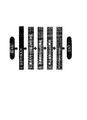
- FIG. 2 shows a configuration diagram of the scaled element filter in the present embodiment.
- the figure shows a filter obtained by scaling the basic filter by p + 1 times.
- This basic low-pass filter includes delay elements 21-1, 21-2, 21-3, 21-4, 21-5, and 21-6 that are delayed by p + 1 samples, and multipliers 22-1, 22-2, and 22-3. And adders 23-1, 23-2, 23-3 and 23-4.
- the filter coefficients of the multipliers 22-1 to 22-3 are ⁇ 1/16, 9/16, and 1, respectively.
- the multiplier 22-3 can be omitted because the coefficient is 1.
- This filter represents an arithmetic circuit of the following equation.
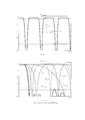
- FIG. 14 is an explanatory diagram of changes in frequency characteristics due to the cascade connection of basic filters.
- the scaled low-pass filter L pk (z) in cascade as shown in FIG. 1, for example, a filter having a frequency characteristic shown in FIG. 14 can be realized.
- the scaled filters in cascade features such as a narrow passband width and a sufficiently low stopband can be found.
- the first stage shows the case of the basic filter L 0
- the second stage shows the case where the basic filter L 0 and the filter L 1 are connected in cascade.
- the third stage shows a case where the basic filter L 0 , the filter L 1 and the filter L 2 are connected in cascade.
- the cascade connection of the scaled filters makes it possible to narrow the passband width and reduce the stopband.
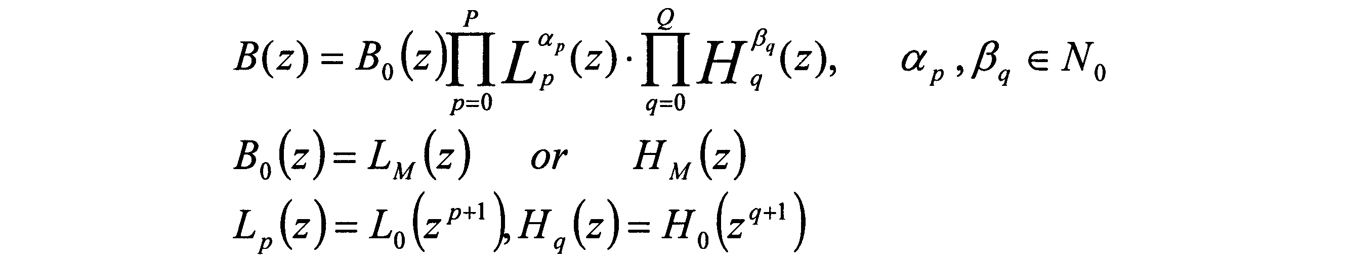
- the filter X (z) can be generally expressed by the following equation.
- L 0 is a low-pass basic filter (mother filter).
- H 0 is a high-pass basic filter (mother filter).
- p and q are scaling numbers (scaling factors). That is, the filter is obtained by scaling the frequency by p + 1 times or q + 1 times.
- ⁇ p is the number of connections of the same scaling filter, and is the number of connections (power value) of the low-pass filter scaled by p + 1.
- ⁇ q is the number of connections of the same scaling filter, and is the number of connections (power value) of the high-pass filter scaled q + 1 times.
- H Q (z) H 0 (z Q + 1 )
- the highest orders p and q at that time are P and Q.
- the relationship between the target bandwidth fp and the bandwidth f 0 of the mother filters L 0 and H 0 is expressed by the following equation.
- the bandwidth can be reduced in the pass band, and the unnecessary band can be attenuated in the stop band.
- the present embodiment is to make use of this characteristic to constitute a filter with a small number of taps.
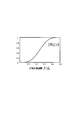
- FIG. 15 is an explanatory diagram of the bandpass filter according to the present embodiment. This figure shows the characteristics of the filter to be realized, which is a design target. The following items are given as the requirements of the filter to be realized. The relationship between the symbols is shown in FIG. (1) Sampling frequency fs (2) Center frequency fc (3) Cutoff frequency (frequency of 3 dB attenuation) f 1 , f ⁇ 1 (4) Passband frequency width (-3 dB bandwidth) ⁇ fb (5) Stopband frequency f 2 , f ⁇ 2 (6) Stop band attenuation Ad (dB)
- the sampling frequency fs is the repetition frequency of the signal input to the filter
- the center frequency fc is the center frequency of the filter extracted from the frequency components included in the signal.
- the cut-off frequency f 1 is the maximum frequency that allows the signal to pass
- the target f ⁇ 1 across the center frequency fc is the minimum frequency that allows the signal to pass.
- the attenuation of the passing signal with respect to the original signal at the cutoff frequencies f 1 and f ⁇ 1 is ⁇ 3 dB.
- An appropriate value other than ⁇ 3 dB may be set as a reference.
- This attenuation A is defined by the following equation, where X is the magnitude of the input signal and Y is the magnitude of the filter output signal at the cutoff frequency. That is, at the cutoff frequencies f 1 and f ⁇ 1 , it means that a signal attenuated to about 70.8% (1 / ⁇ 2) of the input signal is output. This represents that the amplitude energy of the signal is attenuated to 1 ⁇ 2.
- a signal passing band is defined between the cutoff frequencies f 1 and f ⁇ 1 and the frequency width ⁇ fb (m) is given by the following equation.
- the cutoff frequency f 1, f A transition band characteristic that attenuates from an attenuation level of ⁇ 1 (for example, ⁇ 3 dB) to an attenuation degree Ad is given.
- ⁇ 1 for example, ⁇ 3 dB
- Ad attenuation degree
- an appropriate value may be set as a reference.
- the attenuation degree Ad in the stop band is ⁇ 80 dB
- the ratio of the magnitude of the input signal X and the filter output signal is 0.01% as follows.
- FIG. 16 is an explanatory diagram of the frequency shift of the bandpass filter of this embodiment.
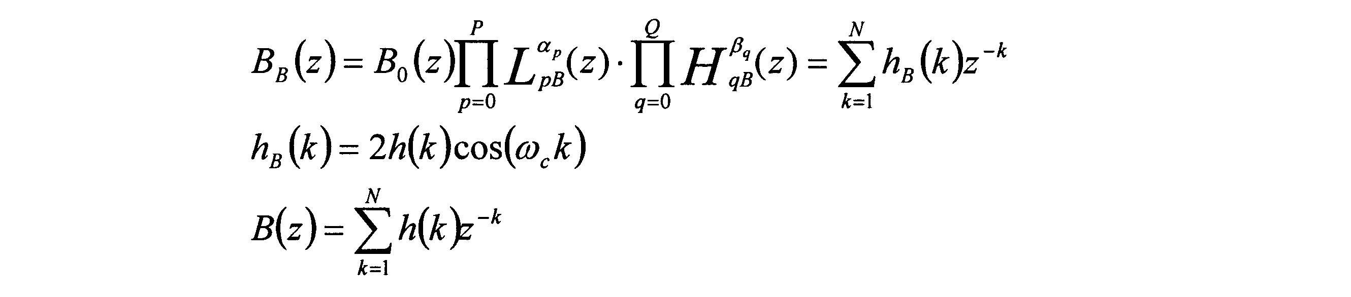
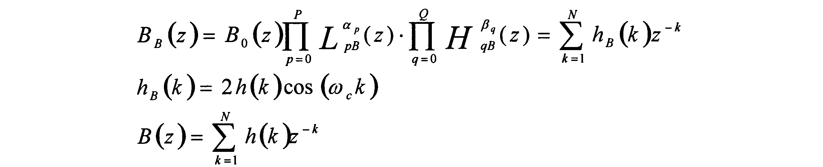
- the filter B B (z) is converted into a form obtained by multiplying the coefficient of the filter B (z) by 2 cos ( ⁇ c k). From this, first, it is only necessary to convert the requirements into the following items and design the filter B (z).
- FIG. 21 is an explanatory diagram of the bandpass filter according to the present embodiment. This figure shows the characteristics of the filter to be realized, which is the design goal described above.
- Sampling frequency fs (2) Center frequency 0
- Cutoff frequency (eg, frequency of 3 dB attenuation)
- Passband frequency width (eg, -3 dB bandwidth) ⁇ fb
- Stop band attenuation Ad (dB) (Example: -80 dB)
- L p (z) is a low-pass filter obtained by scaling the basic low-pass filter L 0 (z) by p + 1.
- H q (z) is a high-pass filter obtained by scaling the basic high-pass filter H 0 (z) by q + 1.
- M is a scale value determined from the frequency width of the passband
- P and Q ( ⁇ M) indicate scale values smaller than M.
- ⁇ p and ⁇ q indicate powers of the same L p (z) and H q (z), and indicate that ⁇ p and ⁇ q are cascaded.
- the filter B 0 (z) is L M (z) in the case of the low-pass filter format, and H M (z) in the case of the high-pass filter format.
- FIG. 17 is a diagram illustrating the relationship between the passband frequency width and the scaling factor according to this embodiment.
- the maximum scale value M is determined from the required passband frequency width ⁇ fb.
- the frequency width ⁇ fb of the pass band becomes narrower as the scale value becomes larger. Therefore, there is a relationship shown in FIG. 17 between ⁇ fb and the scale value p (or q).
- FIG. 19 is a diagram illustrating a configuration example of the band-pass filter according to the present embodiment.
- the bandpass filter is designed with the configuration example shown in the figure.
- This filter is a filter B 0 maximum scale value (z), 0B, ... and the low-pass filter L 0B, ... filter the L pB alpha p and cascaded scaled by pB, 0B, high pass filter scaled ... qB
- a filter in which H 0B ,... H qB are connected in ⁇ q stages is provided.
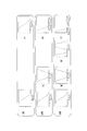
- FIG. 22 shows a configuration diagram of the basic low-pass filter L 0B (z).
- the basic low-pass filter L 0B (z) as in the above equation is specifically represented by the illustrated circuit configuration.
- This basic low-pass filter includes delay elements 21-1, 21-2, 21-3, 21-4, 21-5, and 21-6 that are delayed by one sample, and multipliers 22-1, 22-2, and 22-3. , 22-4 and 22-5, and adders 23-1, 23-2, 23-3 and 23-4.
- the filter coefficients of the multipliers 22-1 to 22-5 are ⁇ 1/8, 9/8 cos (2 ⁇ c ), 2 cos (3 ⁇ c ), 9/8 cos (4 ⁇ c ), and ⁇ 1/8 cos (6 ⁇ c ), respectively. ).
- FIG. 23 shows a configuration diagram of the low-pass filter L pB (z) scaled by p + 1.
- the low-pass filter L pB (z) scaled by p + 1 times has the same structure as L 0B as shown in the figure, but Z ⁇ 1 becomes Z ⁇ (p + 1) .
- This low-pass filter scaled by p + 1 times includes blocks 31-1, 31-2, 31-3, 31-4, 31-5 and 31-6 having p + 1 delay elements, and multipliers 32-1, 32. -2, 32-3, 32-4 and 32-5, and adders 33-1, 33-2, 33-3 and 33-4.
- each delay element 31-1 to 31-6 has (p + 1) delay elements.
- Each block of delay elements may be any number as long as it is a delay element that is delayed by (p + 1) samples.
- FIG. 25 shows a configuration diagram of the high-pass filter H qB (z) scaled by q + 1 times.
- the high-pass filter H qB (z) scaled by q + 1 times has the same structure as H 0 as shown, but Z ⁇ 1 becomes Z ⁇ (q + 1) .
- the high-pass filter scaled q + 1 times includes blocks 51-1, 51-2, 51-3, 51-4, 51-5 and 51-6 having q + 1 delay elements, and multipliers 52-1, 52. -2, 52-3, 52-4 and 52-5 and adders 53-1, 53-2, 53-3 and 53-4.
- each delay element 51-1 to 51-6 has (q + 1) delay elements.
- Each block of delay elements may be any number as long as it is a delay element that is delayed by (q + 1) samples.
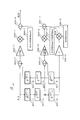
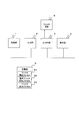
- FIG. 32 is a hardware configuration diagram of the design system according to the present embodiment.
- This design system includes a processing unit 1, which is a central processing unit (CPU), an input unit 2, an output IF unit 3, a display unit 4, a storage unit 5, and a filter circuit 6. Further, the processing unit 1, the input unit 2, the output IF unit 3, the display unit 4, and the storage unit 5 are connected by appropriate connection means such as a star or a bus. The processing unit 1 accesses the storage unit 5 and executes processing for designing a filter.
- CPU central processing unit
- the processing unit 1 accesses the storage unit 5 and executes processing for designing a filter.
- the storage unit 5 stores a filter configuration file 51 for storing design specifications and requirements (for example, conditions (range, value, ratio, etc.) for the pass band and the stop band and upper limit of the number of filter cascade connections ⁇ p , ⁇ q , etc.).
- design specifications and requirements for example, conditions (range, value, ratio, etc.) for the pass band and the stop band and upper limit of the number of filter cascade connections ⁇ p , ⁇ q , etc.
- the low-pass filter L 0 was basic low-pass filter and scaling as described above, L 1, ⁇ ⁇ ⁇ , L p, ⁇ ⁇ ⁇ , lowpass multiplied by 2cos ( ⁇ c k) in each filter coefficients of these filters L p A filter L pB , a basic high-pass filter and a scaled high-pass filter H 0 , H 1 ,..., H q ,..., A high-pass filter that multiplies each filter coefficient of these filters H q by 2 cos ( ⁇ c k) H qB, basic filter characteristic file 52 for storing the characteristics of, and data parameters for determining the filter structure designed (example In the filter for storing the shift amount B, the maximum scale value M, the filter coefficients of the multiplier, p, q, alpha p, intermediate result by the processing unit 1 of the filter characteristics or the like which is beta p, etc.) and design and the final results, etc.
- FIG. 18 is a flowchart showing the processing procedure of the present embodiment.
- the design system configures the filter by the following steps S01 to S07.
- Step S01 The processing unit 1 receives desired characteristic data that becomes design specifications / requirements including, for example, a center frequency fc, a cutoff frequency f1, a stopband frequency f2, a passband attenuation A, a stopband attenuation Ad, and a sample frequency fs.
- desired characteristic data that becomes design specifications / requirements including, for example, a center frequency fc, a cutoff frequency f1, a stopband frequency f2, a passband attenuation A, a stopband attenuation Ad, and a sample frequency fs.
- desired characteristic data that becomes design specifications / requirements including, for example, a center frequency fc, a cutoff frequency f1, a stopband frequency f2, a passband attenuation A, a stopband attenuation Ad, and a sample frequency fs.
- step S01 the processing unit 1 reads each value of the set characteristic data from the storage unit 5 (filter configuration file 51), and shifts the center frequency fc to the origin 0 by the following equation based on the input characteristic data.
- the shift amount B to be calculated is calculated.
- B [fc / fs] ([] indicates rounding to the nearest decimal place.)
- the processing unit 1 stores the obtained shift amount B in the storage unit 5 (filter output file 53).
- the processing unit 1 in accordance with the shift amount B, converts the center frequency fc of the input characteristic data, a cut-off frequency f1, the stopband frequency f2 respectively, the center frequency 0, the cutoff frequency f a, the stopband frequency f b
- Each value is stored in the storage unit 5 (filter output file 53).
- the processing unit 1 reads each value of the set characteristic data from the storage unit 5 (filter configuration file 51), and calculates the maximum order scale value (scaling factor) M based on the input characteristic data. To do.
- the processing unit calculates a passband width ⁇ fb (M) of a filter obtained by scaling the scale value (maximum scale value) M of the highest order by, for example, M + 1 times as follows.
- Passband width ⁇ fb (M) (f1 ⁇ fc) * 2
- the processing unit 1 refers to a scaling curve stored in advance in the storage unit 5 (basic filter characteristic file 52) or calculates from a relational expression of the scaling curve to thereby obtain a passband width ⁇ fb ( The maximum scale value M is obtained according to M).
- the processing unit 1 may determine the maximum scale value M in advance by the input unit 2 or the storage unit 5.
- the processing unit 1 stores the obtained maximum scale value M in the storage unit 5 (filter output file 53).
- the maximum values of ⁇ p and ⁇ q are set in advance in the storage unit 5 (filter configuration file 51) and the processing unit 1 selects from the maximum values in descending order, for example, and p, By selecting q in descending order from the maximum scale value M, an optimal selection of a combination of p, q, ⁇ p , ⁇ q can be performed.
- Step S07 The processing unit 1 reads out specification data and parameters for constructing a filter such as p, q, ⁇ p , and ⁇ q from the storage unit 5 (filter output file 53), and further stores the storage unit 5 (basic filter characteristic file 52).
- the characteristics of the filter L 0M or the filter H 0M corresponding to B 0 (z) according to the low-pass filter or the high-pass filter, and the characteristics of the filter L pB and the filter H qB are read out from the filter B B (z) And the filter characteristics and use data / parameters are displayed on the display unit 4 and / or stored in the storage unit 5 (filter output file 53).
- the processing unit 1 reads specification data and parameters for constructing a filter such as p, q, ⁇ p , ⁇ q and the like from the storage unit 5 (filter output file 53), and also stores the storage unit 5 (basic filter characteristics).
- the characteristics of the filter L pB and the filter H qB can be read from the file 52), and each value can be output to the filter circuit 6 via the output IF unit 3.
- the processing unit 1 may form the filter B B (z) by the filter circuit 6 according to each read value.
- the filter circuit 6 can form the filter B B (z) by computer simulation or software. Further, the filter circuit 6 may form the filter B B (z) by hardware according to each value output from the output IF unit 3.
- the quantization expansion method is a method of realizing the same characteristic as the impulse response characteristic with the illustrated filter circuit configuration based on the cascade-structured filter designed as described above.
- L p (z) L 0 (z p + 1 )
- the impulse signal is input to the filter having the cascade connection structure designed in (1) to obtain the response.
- the impulse response can be calculated by, for example, a well-known simulation software such as MATLAB, and the impulse response waveform can be obtained.
- X (z) mathematical calculation software such as MATTHEMATICA.
- the expansion equation is an impulse response function of X (z). Therefore, a filter can be configured by using the impulse response coefficient C k as a filter coefficient.
- FIG. 27 shows an example of a filter configuration diagram.
- This filter includes multipliers 72-0 to 72-k, delay elements 71-1 to k that delay one sample, and adders 73-1 to 73-k.
- the processing unit 1 reads data (filter coefficients, p, q, ⁇ p , ⁇ q, etc.) for configuring a filter from the storage unit 5 (filter output file 53), and uses the filter circuit 6 or the like, An impulse response is obtained, and a coefficient C k of the impulse response is stored in the storage unit 5 (filter output file 53).
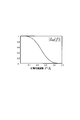
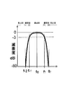
- FIG. 29 is a frequency characteristic diagram of a filter designed by each method using theoretical values. As shown in the left figure, the Remez method satisfies the specifications, but ripples are generated in the passband and the stopband. On the other hand, in the filter according to the present invention, as shown in the right figure, the specification is satisfied, and a large attenuation is observed in the stop band.
- FIG. 30 shows a frequency characteristic diagram of a filter designed by each method after coefficient quantization. As shown in the left figure, in the Remez method, errors are conspicuous over the entire stop band. On the other hand, in the filter according to the present invention, it can be seen that the error is only slightly observed in the transition region as shown in the right figure.
- FIG. 31 shows the evaluation of the filter according to the present invention against the required specifications.
- the filter according to the present invention can be realized with a very small number of taps as compared with the conventional method.
- the filter configuration (design) method or filter configuration (design) apparatus / system of the present invention records a filter configuration (design) program and a filter configuration (design) program for causing a computer to execute each procedure.
- the program can be provided by a computer-readable recording medium, a program product including a filter configuration (design) program and loadable into an internal memory of the computer, a computer such as a server including the program, and the like.
- FIG. 33 shows a circuit diagram of the filter G.
- FIG. 34 shows a circuit diagram of G pass .
- FIG. 35 and FIG. 36 show developed views of G pass .
- FIG. 35 shows the previous term part of G pass .
- FIG. 36 shows the latter term part of G pass .
- N1 N p ( 1)
- N2 N p (2)
- N P (1) L p , the number of stages of the ladder connection H P in N1 (indicating the diagonal connection stages of FIG. 35.)
- N P (2) The number of ladder connections of L P in [1-H p, N2 ] (shows the number of diagonally connected stages in FIG. 36).
- P Indicates a filter whose frequency is scaled by (P + 1) times. About scaling, it becomes the relationship of the following formula.
- FIG. 37 shows a circuit diagram of G stop .
- the stop band main part G stop is formed in the same manner.
- G stop is expressed by the following equation.
- ⁇ k , ⁇ l power value ( indicating that the same L pk, Nk and [1-H ql, Nl ] are connected ⁇ k times and ⁇ l times)
- N k The number of stages of ladder connection of H p at L pk and Nk (shows the number of diagonal connection stages in FIG. 35 (corresponding to N p (1) ).
- N l [1-H ql , Nl] number of ladder connected between L P in (indicating the corresponding to diagonal connection stages of FIG.
- FIG. 38 is a hardware configuration diagram according to the present embodiment.
- This hardware includes a processing unit 1, which is a central processing unit (CPU), an input unit 2, an output IF unit 3, a display unit 4, a storage unit 5, and a filter circuit 6. Further, the processing unit 1, the input unit 2, the output IF unit 3, the display unit 4, and the storage unit 5 are connected by appropriate connection means such as a star or a bus.
- the storage unit 5 includes a filter configuration file 51 that stores design specifications and conditions (for example, conditions (range, value, ratio, etc.) for the pass band and the stop band, and an upper limit N pass for the number of multipliers), as described above.
- Basic low-pass filter and scaled low-pass filter (L 0 , L 1 ,..., L m ,...), Basic high-pass filter and scaled high-pass filter (H 0 , H 1 ,..., H m,. ..) basic filter characteristic file 52 for storing characteristics and data parameters (for example, filter coefficients N pass , N p (1) , N p (2) of the multiplier) for defining the designed filter configuration ⁇ p, ⁇ p, P, N k, N l, ⁇ pk, ⁇ pl, p k, q l , etc.) and designed intermediate result by the processing unit 1 of the filter characteristics and the final result, and the like
- a filter output file 53 for storing.
- Each of these data can be output by the processing unit 1 to the filter circuit 6 (for example, data parameters for determining a filter configuration such as a filter coefficient of a multiplier) via the output IF unit 3.
- the filter circuit 6 is configured by software or hardware, and implements a filter having a predetermined characteristic according to each set data by the processing unit 1 via the output IF unit 3.
- Design specification setting (S0)
- the processing unit 1 stores the design specifications (for example, conditions (range, value, ratio, etc.) for the pass band and the stop band and the upper limit N pass of the number of multipliers, etc.) according to the operation from the input unit 2. It is set in advance by storing it in the configuration file 51) or by reading the value stored in the storage unit 5 (filter configuration file 51) stored in advance.
- FIG. 40 is a diagram illustrating the cutoff characteristics of the product-sum module cascade connection model G (f).
- f 3 and f 80 are as follows.
- the steep cut-off characteristic is expressed by the following equation, for example, by a value R (0 ⁇ R ⁇ 1) representing a ratio between f 3 and f 80 .
- R f 3 / f 80 ⁇ 1
- the processing unit 1 can set the design specifications as follows, for example. Pass band [0, f 3 ] is ⁇ 3 [dB] or more Stop band [f 80 , 1] is ⁇ 80 [dB] or less R ⁇ R 0 (the calculated filter ratio R is a predetermined ratio R 0 or more (Indicates that However, 0 ⁇ f 3 ⁇ f 80 ⁇ 1, 0 ⁇ R 0 ⁇ 1
- Step S1 (Determination of the maximum value of p)
- the processing unit 1 may determine the value of P in advance by the input unit 2 or the storage unit 5 (filter output file 53). That is, the processing unit 1 uses f 3 (p) as a point -3 [dB] of L p , f 3 (0) is obtained in advance, and then Let P be the smallest p.
- the processing unit 1 stores the obtained P in the storage unit 5 (filter output file 53).
- the processing unit 1 reads the characteristics of the corresponding low-pass filter and high-pass filter determined by N p (1) , N p (2) , ⁇ p , ⁇ p from the storage unit 5 (basic filter characteristic file 52),
- the G pass characteristic is calculated by the above equation, and the combination having the minimum number of multipliers is selected from the combinations that satisfy the design specifications (eg, R ⁇ R 0 ).
- the processing unit 1 may further select one that matches the design specifications of the passband and the stopband.
- the following are defined as combination rules.
- the processing section 1 is In (N k , N l , ⁇ pk , ⁇ ql ) ⁇ ⁇ 0, 1, 2 ,.
- G G pass G stop
- the combination having the minimum number of multipliers is selected from the combinations having the design specifications (for example, R ⁇ R 0 ).
- Step S4. G configuration and output
- the processing unit 1 is configured to store N p (1) , N p (2) , ⁇ p , ⁇ p , N k , N l , ⁇ pk , ⁇ pl, etc. from the storage unit 5 (filter output file 53).
- G G pass G stop
- the processing unit 1 the storage unit 5 from (filter output file 53) N p (1), N p (2), ⁇ p, ⁇ p, N k, N l, ⁇ pk, ⁇ filters such as pl
- the specification data and parameters for configuration are read, and each value is output to the filter circuit 6 via the output IF unit 3.
- the filter circuit 6 can form the filter G by computer simulation or software.
- the filter circuit 6 may form the filter G by hardware according to each value output from the output IF unit 3.
- FIG. 41 is an explanatory diagram of low-pass filter specifications.
- a configuration example of a low-pass filter is given according to the above-described configuration means.
- the specifications of desired characteristics are as shown in the figure.
- the passband and stopband are sections with normalized frequencies.
- select P 7,
- G pass L 3 Set to 7,9 .
- FIG. 42 is an explanatory diagram of the G pass and G stop and the filter G.
- FIG. 42A shows a G pass characteristic diagram.
- the stop band the second to fourth side lobes of G pass must be blocked, but for the third and fourth side lobes, (1-H 1 1,1 ) in FIG. And (1-H 1 2,1 ) is almost blocked.
- P ⁇ 5 is assumed, and as can be seen from FIG. 26 (b), the vicinity of the second side lobe center is L 1 3,1 and L 1 4,2 , and the right side is L 1 3,1 .
- FIG. 43 is a characteristic diagram of a filter configured by the conventional method and the present invention.
- (A) is the least square method
- (b) is the Remez method
- (c) is the method according to the present invention.
- FIG. 44 is a diagram showing a comparison between the number of multipliers and R in each design method.
- the number of multipliers is the one when the characteristic first meets the specification completely.
- the method according to the present invention is superior in both the number of multipliers and R as compared with the method of least squares.
- R is slightly superior to the method according to the present invention, but the number of multipliers is as large as 1142.
- the effectiveness of the steep low-pass filter characteristic approximation model by the cascade connection of the element filters by the product-sum module according to the present invention was shown.
- a piecewise m-order polynomial can be used as the impulse response function, and an interpolation function with a waveform adjustment parameter or the like may be used.
- the present invention is applied to various technologies such as audio technology, video technology, image technology, transmission technology, communication technology, analog-digital conversion / digital-analog conversion technology, compression / decompression technology, encryption / decryption (decompression) technology, filter technology, etc. can do.
- the present invention can be widely used as a filter for signal processing in sound, image, communication, and the like. Further, the present invention can be used for various devices such as an acoustic device such as an amplifier, an image device for processing moving images and still images, a communication device such as a mobile phone, a control device, a computer, and a PC.
Landscapes
- Engineering & Computer Science (AREA)
- Physics & Mathematics (AREA)
- Computer Hardware Design (AREA)
- Mathematical Physics (AREA)
- Computing Systems (AREA)
- Theoretical Computer Science (AREA)
- Tone Control, Compression And Expansion, Limiting Amplitude (AREA)
- Filters And Equalizers (AREA)
- Compression, Expansion, Code Conversion, And Decoders (AREA)
- Filters That Use Time-Delay Elements (AREA)
Abstract
少ない入力タップ数、遅延回路、乗算器で所定の特性を得ることが可能で、且つ応答性の向上、低コスト化を図るFIRフィルタを実現すること。 FIRフィルタによるローパスフィルタ、バンドパスフィルタ、ハイパスフィルタにおいて、基本インパルス応答関数を与え、そのインパルス応答関数から決定されるフィルタ係数を持つ基本フィルタを構成し、該基本フィルタの時間スケールあるいは周波数スケールを変更することにより、周波数特性の異なるフィルタを構成する。この特性の異なるフィルタを縦続形式、あるいは階段形式に組み合わせることでタップ数の少ないFIRフィルタを構築する。
Description
本発明は、フィルタに係り、特に、タップ数が少なく、急峻な減衰特性を持つFIR(Finite Impulse Response:有限インパルス応答)フィルタに関する。
近年におけるマルチメディア情報のディジタル化に伴い、ディジタル信号処理を実現する演算処理アルゴリズムや演算処理回路の重要性が増してきている。その中でもディジタルフィルタは、雑音除去、周波数特性の調整、信号分離などに利用されている。特に、インパルス応答が有限なFIRフィルタは、有界な入力に対しては常に安定性が保証され、インパルス応答が対称の場合、FIRフィルタは完全な線形位相を実現できる。線形位相は波形伝送、計測、音声再生などにおいて重要となる性質である。しかしながら、フィルタの周波数特性に要求される精度とフィルタの規模との間にはトレードオフの関係があり、より急峻な特性を得るためには高次の伝達特性が必要となり、回路的には乗算器、遅延素子などが多大に必要になるという課題がある。例えば、帯域が非常に狭い帯域通過型のフィルタを設計する場合、伝達特性の次数は顕著に高くなり、それに応じた多くの乗算器が必要になる。
このような背景から、これまで多くの提案がなされてきた。下記非特許文献1には、従来法として通常利用されているRemezの方法が記載されている。また、非特許文献2には、縦続構成による低感度な線形位相FIRフィルタの一構成法が記載されており、縦続構成によって乗算器の低減を図っている。さらに、特許文献1には、フィルタ出力信号の遅延を可変とすることを目的とするFIRフィルタが記載されている。
その他にも、従来より、音響信号における帯域分離のためのフィルタや画像のノイズ除去のためのフィルタなど、用途に応じたFIRフィルタが検討されている。
その他にも、従来より、音響信号における帯域分離のためのフィルタや画像のノイズ除去のためのフィルタなど、用途に応じたFIRフィルタが検討されている。
さらに、従来技術として、例えば、非特許文献3には、低折返しマルチレベルFIRフィルタのための非最大間引きフィルタバンクの設計と実装について開示されている。
また、非特許文献4には、低折返し雑音で所望周波数特性を実現するフィルタバンクが開示されている。
さらに、非特許文献5には、完全再構成非最大間引きコサイン変調フィルタバンクの一実現法が開示されている。
また、特許文献2には、実数値を持つ信号に対する最大間引きフィルタバンクと、その特別の場合であるコサイン変調フィルタバンクを効率的に実現することができるフィルタバンク及びフィルタリング方法が開示されている。
また、非特許文献4には、低折返し雑音で所望周波数特性を実現するフィルタバンクが開示されている。
さらに、非特許文献5には、完全再構成非最大間引きコサイン変調フィルタバンクの一実現法が開示されている。
また、特許文献2には、実数値を持つ信号に対する最大間引きフィルタバンクと、その特別の場合であるコサイン変調フィルタバンクを効率的に実現することができるフィルタバンク及びフィルタリング方法が開示されている。
D.Shpak、"A generalized Remez method for the design of FIR digital filters、" IEEE Trans. Circuit System、vol.37、no.2、pp.161-174、Feb. 1990.
本間仁志、森幸雄、佐川雅彦、"縦続構成による低感度な線形位相FIRフィルタの一構成法、"信学論、vol.J70-A、no.5、pp.766-774、May.1987.
河野、高沢他 「低折返しマルチレベルFIRフィルタのための非最大間引きフィルタバンクの設計と実装」 計測自動制御学会東北支部 第229回研究集会(2006.6.9) 資料番号 229-8 p1-11
高沢、阿部他 「低折返し雑音で所望周波数特性を実現するフィルタバンク」 計測自動制御学会東北支部 第215回研究集会(2004.5.27) 資料番号 215-7 p1-10
伊丹、渡部他 「完全再構成非最大間引きコサイン変調フィルタバンクの一実現法」 電子情報通信学会論文誌 A Vol.J83-A No.9 pp.1037-1046 2000年9月
しかしながら、従来の技術においては、いずれのフィルタにおいても、乗算器(ソフト演算の場合は乗算回数)や遅延素子(ソフト処理の場合はメモリ数)の飛躍的低減には結びついていない。
例えば、上述した非特許文献1では、急峻な減衰特性を有するフィルタを実現するためには膨大な乗算器や遅延素子が必要となる。また、上述した非特許文献2では、低感度なフィルタを対象としており、急峻な減衰特性を有するフィルタには適さない。
例えば、上述した非特許文献1では、急峻な減衰特性を有するフィルタを実現するためには膨大な乗算器や遅延素子が必要となる。また、上述した非特許文献2では、低感度なフィルタを対象としており、急峻な減衰特性を有するフィルタには適さない。
このように、従来法では急峻な減衰特性を持つ高性能フィルタを構成する場合、膨大な入力タップ数、遅延回路、乗算器を必要とし、所定の特性を持つフィルタ出力が安定するまで長大な経過時間を要していた。
さらに、近年、音、映像などのマルチメディアが音響信号圧縮(MP3)や映像信号圧縮(MPEG)等の形式で配信されているが、情報の洪水や、ジャギー等の発生による品質劣化が課題となっている。また、圧縮処理において、周波数領域での帯域分離が行われるが、過大な乗算器や遅延素子が必要となっている。
さらに、近年、音、映像などのマルチメディアが音響信号圧縮(MP3)や映像信号圧縮(MPEG)等の形式で配信されているが、情報の洪水や、ジャギー等の発生による品質劣化が課題となっている。また、圧縮処理において、周波数領域での帯域分離が行われるが、過大な乗算器や遅延素子が必要となっている。
また、その他にも、従来のREMEZフィルタはSINC函数(無限区間の函数)を基本函数としているため、実際の回路では有限区間に打ち切る必要があるので、ノイズの発生原因となる可能性があることが分かっている。
本願発明は、以上の点に鑑み、少ない入力タップ数、遅延回路、乗算器で所定の特性を得ることが可能で、応答性の向上、低コスト化を図るフィルタを提供することを目的の一つとする。
本願発明は、以上の点に鑑み、少ない入力タップ数、遅延回路、乗算器で所定の特性を得ることが可能で、応答性の向上、低コスト化を図るフィルタを提供することを目的の一つとする。
本発明はまた、ノイズ除去特性に優れた低コストなFIRフィルタ提供することを目的の一つとする。
また、本発明は、ジャギー等を発生させない信号処理に適切なFIRフィルタを提供することを目的の一つとする。
なお、FIRフィルタは、例えば、アンプ等の音響装置、動画、静止画処理のための画像装置、携帯電話等の通信装置、制御装置、コンピュータ、PC等の様々な各種装置に用いることができる。
また、本発明は、ジャギー等を発生させない信号処理に適切なFIRフィルタを提供することを目的の一つとする。
なお、FIRフィルタは、例えば、アンプ等の音響装置、動画、静止画処理のための画像装置、携帯電話等の通信装置、制御装置、コンピュータ、PC等の様々な各種装置に用いることができる。
本発明の主な特徴のひとつは、有限台のn次区分多項式で表したインパルス応答関数を基本関数とし、該関数の節点値をフィルタ係数とするため、従来のSINC関数を基本関数とするフィルタに比べ、入力信号のサンプル点は少なくなり、周波数特性も台の打ち切り誤差や折り返し誤差などの無いフィルタを構成することができる。
本発明の他の特徴は、前記n次区分多項式は2~4次の関数で良く、通過域での周波数特性はリプルの少ない平坦特性で、且つ線形位相を持つ特徴を有する。
本発明の他の特徴は、前記n次区分多項式は2~4次の関数で良く、通過域での周波数特性はリプルの少ない平坦特性で、且つ線形位相を持つ特徴を有する。
本発明の他の特徴は、基本フィルタを周波数スケーリングすることで、スケール値に応じて通過域を狭めることが可能となり、さらに零点の数を増加させるため阻止域での減衰度を高めることができることにある。
本発明の他の特徴として、前記スケーリングされたフィルタを縦続接続することにより、乗算器が少なく、高性能なフィルタを構成できる。
本発明の他の特徴として、前記スケーリングフィルタの縦続接続は、通過域幅が所望の通過域幅と同じあるいは広い通過域幅を持つローパス型およびハイパス型のスケーリングフィルタを組み合わせることにあり、遮断周波数を所望の値に確保することにある。
本発明の他の特徴として、阻止域の減衰度を評価値として、スケーリングフィルタの選択を行うため、阻止域の減衰度を非常に大とすることにある。
本発明の他の特徴として、前記スケーリングされたフィルタを縦続接続することにより、乗算器が少なく、高性能なフィルタを構成できる。
本発明の他の特徴として、前記スケーリングフィルタの縦続接続は、通過域幅が所望の通過域幅と同じあるいは広い通過域幅を持つローパス型およびハイパス型のスケーリングフィルタを組み合わせることにあり、遮断周波数を所望の値に確保することにある。
本発明の他の特徴として、阻止域の減衰度を評価値として、スケーリングフィルタの選択を行うため、阻止域の減衰度を非常に大とすることにある。
本発明の第1の解決手段によると、
有限台の区分的多項式で構成されるインパルス応答函数の節点値を係数とする低域通過/高域通過型の基本フィルタを構成し、該基本フィルタを時間軸あるいは周波数軸でスケーリングした複数のスケーリングフィルタを組み合わせて所望の特性とすることを特徴とするFIRフィルタが提供される。
有限台の区分的多項式で構成されるインパルス応答函数の節点値を係数とする低域通過/高域通過型の基本フィルタを構成し、該基本フィルタを時間軸あるいは周波数軸でスケーリングした複数のスケーリングフィルタを組み合わせて所望の特性とすることを特徴とするFIRフィルタが提供される。
本発明の第2の解決手段によると、
有限台の区分的多項式で構成されるインパルス応答函数の節点値をフィルタ係数とした低域通過型基本フィルタを時間軸又は周波数軸でp+1倍(pは0以上の整数、p=0のとき基本フィルタ)にスケーリングした低域通過型フィルタLp、前記フィルタ係数の符号をひとつおきに反転して係数とした高域通過型基本フィルタを時間軸又は周波数軸でq+1倍(qは0以上の整数、q=0のとき基本フィルタ)にスケーリングした高域通過型フィルタHqと、により、次式で表されるように、フィルタLp及びフィルタHqを縦続接続することで次式のフィルタB(z)のように形成されたフィルタが提供される。
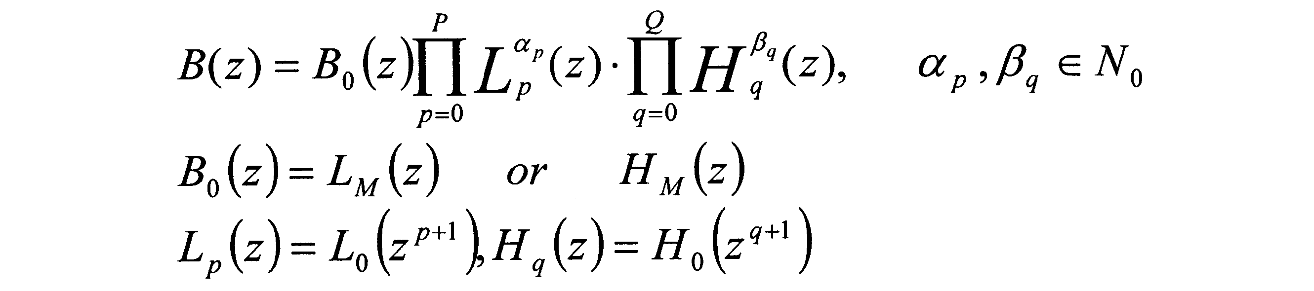
ここで、各添え字については以下の通り。
αp、βp:累乗値(同じLpやHqをαp回、βp回接続することを示す。)
P、Q:スケーリング値p、qの最大値
有限台の区分的多項式で構成されるインパルス応答函数の節点値をフィルタ係数とした低域通過型基本フィルタを時間軸又は周波数軸でp+1倍(pは0以上の整数、p=0のとき基本フィルタ)にスケーリングした低域通過型フィルタLp、前記フィルタ係数の符号をひとつおきに反転して係数とした高域通過型基本フィルタを時間軸又は周波数軸でq+1倍(qは0以上の整数、q=0のとき基本フィルタ)にスケーリングした高域通過型フィルタHqと、により、次式で表されるように、フィルタLp及びフィルタHqを縦続接続することで次式のフィルタB(z)のように形成されたフィルタが提供される。
αp、βp:累乗値(同じLpやHqをαp回、βp回接続することを示す。)
P、Q:スケーリング値p、qの最大値
本発明の第3の解決手段によると、
有限区間の離散入力に係数を乗じて遅延させた信号を順次加算する構成を基本構成とし、その基本構成における遅延素子の数を増減してスケーリングフィルタを構成し、該スケーリングフィルタを縦続接続して信号を出力することを特徴とするフィルタが提供される。
有限区間の離散入力に係数を乗じて遅延させた信号を順次加算する構成を基本構成とし、その基本構成における遅延素子の数を増減してスケーリングフィルタを構成し、該スケーリングフィルタを縦続接続して信号を出力することを特徴とするフィルタが提供される。
本発明の第4の解決手段によると、
有限台の区分的多項式で構成されるインパルス応答函数の節点値を係数とする低域通過/高域通過型の基本フィルタを構成し、該基本フィルタを時間軸あるいは周波数軸でスケーリングした複数のスケーリングフィルタを組み合わせて所望の特性とすることを特徴とするFIRフィルタにおいて、中心周波数、遮断周波数、阻止域周波数、阻止域最高減衰度およびサンプリング周波数を入力し、遮断周波数と中心周波数と決定される通過域周波数幅からスケーリングの最大次数を決定し、該スケーリング次数より少ない次数のスケーリングフィルタを順次選択して、求めるFIRフィルタの阻止域周波数における減衰度が所定の前記最大減衰度以下となるように選択したスケーリングフィルタの採否を判定し、スケーリングフィルタを縦続接続で構成することを特徴とするFIRフィルタが提供される。
有限台の区分的多項式で構成されるインパルス応答函数の節点値を係数とする低域通過/高域通過型の基本フィルタを構成し、該基本フィルタを時間軸あるいは周波数軸でスケーリングした複数のスケーリングフィルタを組み合わせて所望の特性とすることを特徴とするFIRフィルタにおいて、中心周波数、遮断周波数、阻止域周波数、阻止域最高減衰度およびサンプリング周波数を入力し、遮断周波数と中心周波数と決定される通過域周波数幅からスケーリングの最大次数を決定し、該スケーリング次数より少ない次数のスケーリングフィルタを順次選択して、求めるFIRフィルタの阻止域周波数における減衰度が所定の前記最大減衰度以下となるように選択したスケーリングフィルタの採否を判定し、スケーリングフィルタを縦続接続で構成することを特徴とするFIRフィルタが提供される。
本発明の第5の解決手段によると、
有限の区分的多項式で構成される標本化函数の節点値をフィルタ係数とした低域通過型基本フィルタL0と、前記低域通過型基本フィルタを周波数スケーリングした複数の低域通過型フィルタLMと、前記フィルタ係数の符号をひとつおきに反転して係数とした高域通過型基本フィルタH0と、前記高域通過型基本フィルタを周波数スケーリングした複数の高域通過型フィルタHMと、により、次式で表されるように縦続接続して形成された通過域部フィルタGpassと、

ここで、Gpassの各添え字については以下の通り。
αP,βP :累乗値(同じLP,N1や[1-HP,N2]をαP回、βP回接続することを示す。ここで、記載の都合上、N1=Np (1),N2=Np (2) とした。)
NP (1) :Lp,N1においてHPのラダー接続の段数
NP (2) :[1-Hp,N2]においてLPのラダー接続の段数
P :周波数を(P+1)倍にスケーリングしたフィルタを示す。
前記低域通過型基本フィルタL0及び前記低域通過型フィルタLM、前記高域通過型基本フィルタH0及び前記高域通過型フィルタHMと、により、次式で表されるように縦続接続して形成された阻止域部フィルタGstopと、

αk,βl:累乗値(同じLpk,Nkや[1-Hql,Nl]をαk回、βl回接続することを示す。)
Nk :Lpk,NkにおいてHpのラダー接続の段数
Nl :[1-Hql,Nl]においてLpのラダー接続の段数
pk,ql:周波数をそれぞれ、(pk+1)、(ql+1)倍にスケーリングしたフィルタを示す。
を備え、
前記通過域部フィルタGpass及び前記阻止域部フィルタGstopを縦続接続することで形成されたフィルタが提供される。
有限の区分的多項式で構成される標本化函数の節点値をフィルタ係数とした低域通過型基本フィルタL0と、前記低域通過型基本フィルタを周波数スケーリングした複数の低域通過型フィルタLMと、前記フィルタ係数の符号をひとつおきに反転して係数とした高域通過型基本フィルタH0と、前記高域通過型基本フィルタを周波数スケーリングした複数の高域通過型フィルタHMと、により、次式で表されるように縦続接続して形成された通過域部フィルタGpassと、
αP,βP :累乗値(同じLP,N1や[1-HP,N2]をαP回、βP回接続することを示す。ここで、記載の都合上、N1=Np (1),N2=Np (2) とした。)
NP (1) :Lp,N1においてHPのラダー接続の段数
NP (2) :[1-Hp,N2]においてLPのラダー接続の段数
P :周波数を(P+1)倍にスケーリングしたフィルタを示す。
前記低域通過型基本フィルタL0及び前記低域通過型フィルタLM、前記高域通過型基本フィルタH0及び前記高域通過型フィルタHMと、により、次式で表されるように縦続接続して形成された阻止域部フィルタGstopと、
Nk :Lpk,NkにおいてHpのラダー接続の段数
Nl :[1-Hql,Nl]においてLpのラダー接続の段数
pk,ql:周波数をそれぞれ、(pk+1)、(ql+1)倍にスケーリングしたフィルタを示す。
を備え、
前記通過域部フィルタGpass及び前記阻止域部フィルタGstopを縦続接続することで形成されたフィルタが提供される。
本発明の第6の解決手段によると、
有限の区分多項式で表されるインパルス応答関数の節点値を係数とする低域通過型フィルタ及び高域通過型フィルタを基本とし、該低域通過型フィルタ及び高域通過型フィルタを周波数スケーリングしたスケーリングフィルタを、通過帯域幅が所定の要求幅以上となる様に選択し、該選択されたスケーリングフィルタを用いて、要求特性を満足する低域通過型のスケーリングフィルタを選定し、該選定された低域通過型のスケーリングフィルタに対して、高域通過型のスケーリングフィルタをラダー状に接続することにより、フィルタの通過域特性を形成することを特徴とするフィルタが提供される。
有限の区分多項式で表されるインパルス応答関数の節点値を係数とする低域通過型フィルタ及び高域通過型フィルタを基本とし、該低域通過型フィルタ及び高域通過型フィルタを周波数スケーリングしたスケーリングフィルタを、通過帯域幅が所定の要求幅以上となる様に選択し、該選択されたスケーリングフィルタを用いて、要求特性を満足する低域通過型のスケーリングフィルタを選定し、該選定された低域通過型のスケーリングフィルタに対して、高域通過型のスケーリングフィルタをラダー状に接続することにより、フィルタの通過域特性を形成することを特徴とするフィルタが提供される。
本発明の第7の解決手段によると、
有限の区分多項式で表されるインパルス応答関数の節点値を係数とする低域通過型フィルタ及び高域通過型フィルタを基本とし、該低域通過型フィルタ及び高域通過型フィルタを周波数スケーリングしたスケーリングフィルタを、通過帯域幅が所定の要求幅以上となる様に選択し、該選択されたスケーリングフィルタを用いて、要求特性を満足する高域通過型のスケーリングフィルタを選定し、該選定された高域通過型のスケーリングフィルタに対して、低域通過型のスケーリングフィルタをラダー状に接続することにより、フィルタの通過域特性を形成することを特徴とするフィルタが提供される。
有限の区分多項式で表されるインパルス応答関数の節点値を係数とする低域通過型フィルタ及び高域通過型フィルタを基本とし、該低域通過型フィルタ及び高域通過型フィルタを周波数スケーリングしたスケーリングフィルタを、通過帯域幅が所定の要求幅以上となる様に選択し、該選択されたスケーリングフィルタを用いて、要求特性を満足する高域通過型のスケーリングフィルタを選定し、該選定された高域通過型のスケーリングフィルタに対して、低域通過型のスケーリングフィルタをラダー状に接続することにより、フィルタの通過域特性を形成することを特徴とするフィルタが提供される。
本発明によると、急峻性の良い基本フィルタをスケーリングしたフィルタで構成するため、周波数分離性が優れ、タップ数や、遅延回路、乗算器の数の少ないローパスフィルタ、ハイパスフィルタ、バンドパスフィルタが実現できる。また、本発明によると、阻止域の減衰度を大きくできるため、ノイズ除去特性に優れたフィルタが実現できる。さらに、本発明によると、タップ数(乗算器の数)が従来のフィルタに比べて非常に低減できるため、低コストなフィルタが可能となる。
本発明の理解を深めるために、実施の形態を用いて具体的に説明する。
1.フィルタ構成
図3に、フィルタ処理の概略説明図を示す。
非再帰形ディジタルフィルタは、インパルス応答が有限個のパルスで表されるので、有限インパルス応答FIR(Finite Impulse Responce)形とも呼ばれる。
1.フィルタ構成
図3に、フィルタ処理の概略説明図を示す。
非再帰形ディジタルフィルタは、インパルス応答が有限個のパルスで表されるので、有限インパルス応答FIR(Finite Impulse Responce)形とも呼ばれる。
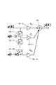
一般にFIRフィルタは、入力信号X(m)、出力信号Y(m)、として図3の様に現在と過去の入力信号に所定の係数(フィルタ係数)C(k)を乗じることで、下記入出力関係から求めることができる。

をFIRローパスフィルタと言う。ただしCk=C(k)である。
図4は、このフィルタの構成図の一例を示す。
このフィルタは、遅延素子31-m~31-(m-p)と、フィルタ係数をそれぞれC0~Cpとする乗算器32-0~32-pと、加算器33を備える。
なお、ハイパスフィルタは下記式で表される。

上式に示したようなローパスフィルタ及びハイパスフィルタにおいて、フィルタ係数Ckはインパルス応答関数から導かれる。
このフィルタは、遅延素子31-m~31-(m-p)と、フィルタ係数をそれぞれC0~Cpとする乗算器32-0~32-pと、加算器33を備える。
なお、ハイパスフィルタは下記式で表される。
図5は、従来のインパルス応答関数波形を示す図である。
従来、インパルス応答関数として、図5に示すSINC関数が適用され、標本間隔の1/2の点における関数値がフィルタ係数Ckとして採用されている。しかし、SINC関数は無限区間の関数であり、フィルタ係数Ckも理想的には無限個必要となる。実際のフィルタにおいては有限個の係数としなければならないが、係数の切り捨てによる誤差や精度を確保するためには係数の個数を非常に多くしなければならないという課題がある。
従来、インパルス応答関数として、図5に示すSINC関数が適用され、標本間隔の1/2の点における関数値がフィルタ係数Ckとして採用されている。しかし、SINC関数は無限区間の関数であり、フィルタ係数Ckも理想的には無限個必要となる。実際のフィルタにおいては有限個の係数としなければならないが、係数の切り捨てによる誤差や精度を確保するためには係数の個数を非常に多くしなければならないという課題がある。
これに対して、図6は、本実施の形態のインパルス応答波形を示す図である。
本実施の形態では、図6に示すような、有限台のインパルス応答関数を用いる。この関数例として、標本点間の1/2区間毎にB-スプライン関数をシフトして合成近似した下記の関数がある。

ここで、h:サンプリング時間間隔
f:周波数
本実施の形態では、図6に示すような、有限台のインパルス応答関数を用いる。この関数例として、標本点間の1/2区間毎にB-スプライン関数をシフトして合成近似した下記の関数がある。
f:周波数
上記関数は例えば特許公開2001-842442によれば次の区分多項式で近似した下記式で表すことができる。

図7は、本実施の形態の離散インパルス応答とフィルタ係数値の説明図である。
図中●印は、有限台のインパルス応答関数の標本点(特異点)を示す。有限台のインパルス応答波形として、図に示す関数ψ(t)が与えられた時、フィルタの遅延時間をサンプリング時間幅hの1/2として、●印の縦軸の値をフィルタ係数(タップ係数)C(k)に与えれば、最も低次のインパルス応答波形が再生される。このフィルタ係数C(k)を持つフィルタを基本ローパスフィルタL0とする。
図中●印は、有限台のインパルス応答関数の標本点(特異点)を示す。有限台のインパルス応答波形として、図に示す関数ψ(t)が与えられた時、フィルタの遅延時間をサンプリング時間幅hの1/2として、●印の縦軸の値をフィルタ係数(タップ係数)C(k)に与えれば、最も低次のインパルス応答波形が再生される。このフィルタ係数C(k)を持つフィルタを基本ローパスフィルタL0とする。
図示のような関数ψでは基本ローパスフィルタは次のように表される。
上式において、図7に示すように各区間のh/2毎の接続点におけるψ(t)の値を係数C(k)にとる。ただし
C(0)=ψ(-1.5)=-1/16
C(1)=ψ(-1.0)=0
C(2)=ψ(-0.5)=9/16
C(3)=ψ(0)=1
C(4)=ψ(0.5)=9/16
C(5)=ψ(1.0)=0
C(6)=ψ(1.5)=-1/16
とする。このとき、基本となるローパスフィルタL0(z)は下記式で表される。

L0(z)は、上述したような定義より
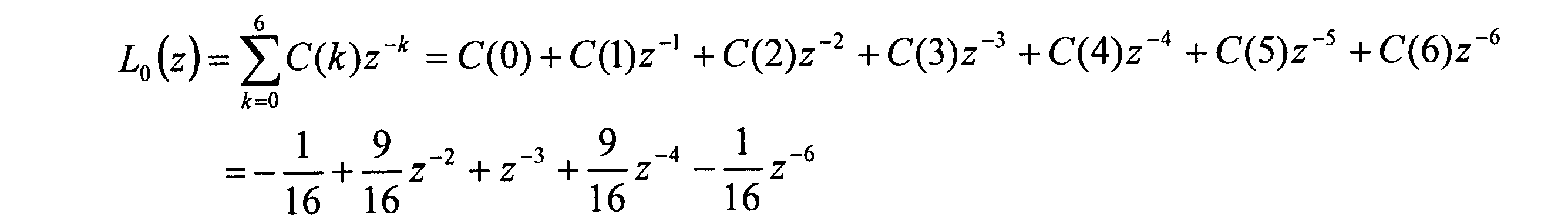
となる。
また、上記基本ローパスフィルタの周波数特性は下記式で表される。

上式において、図7に示すように各区間のh/2毎の接続点におけるψ(t)の値を係数C(k)にとる。ただし
C(0)=ψ(-1.5)=-1/16
C(1)=ψ(-1.0)=0
C(2)=ψ(-0.5)=9/16
C(3)=ψ(0)=1
C(4)=ψ(0.5)=9/16
C(5)=ψ(1.0)=0
C(6)=ψ(1.5)=-1/16
とする。このとき、基本となるローパスフィルタL0(z)は下記式で表される。
また、上記基本ローパスフィルタの周波数特性は下記式で表される。
図8は、本実施の形態のローパスフィルタ周波数応答例を示す図である。この図は、上式の特性を示したものである。
図9に、本実施の形態の基本ローパスフィルタの構成図を示す。
上記基本ローパスフィルタL0の演算回路は一例として図9に示す構成となる。
この基本ローパスフィルタは、遅延素子91-1、91-2、91-3、91-4、91-5及び91-6と、乗算器92-1、92-2、92-3と、加算器93-1、93-2、93-3及び93-4を備える。乗算器92-1~92-3のフィルタ係数は、それぞれ-1/16、9/16、1である。なお、乗算器92-3は、係数が1なので、省略することができる。
次に基本となるハイパスフィルタH0(z)は上記ローパスフィルタL0(z)から下記式で表すことができる。

上記基本ローパスフィルタL0の演算回路は一例として図9に示す構成となる。
この基本ローパスフィルタは、遅延素子91-1、91-2、91-3、91-4、91-5及び91-6と、乗算器92-1、92-2、92-3と、加算器93-1、93-2、93-3及び93-4を備える。乗算器92-1~92-3のフィルタ係数は、それぞれ-1/16、9/16、1である。なお、乗算器92-3は、係数が1なので、省略することができる。
次に基本となるハイパスフィルタH0(z)は上記ローパスフィルタL0(z)から下記式で表すことができる。
図10は、本実施の形態の基本ハイパスフィルタの離散インパルス応答とフィルタ係数値の説明図である。
上式における係数b(k)は、図10の様に係数C(k)の符号を交互に反転した値である。
上式における係数b(k)は、図10の様に係数C(k)の符号を交互に反転した値である。
また、図11は、本実施の形態の基本ハイパスフィルタの周波数応答例を示す図である。
このハイパスフィルタH0(z)の周波数特性は図11に示す特性となり、下記式で表される。

以上のようなフルーエンシDA関数等のインパルス応答関数を使う意義は、例えば、ローカルサポートのためフィルタ係数を有限個の範囲で取り扱うことができ、また、偶関数(線形位相)であるため、線形位相を実現することができることである。さらに、最大平坦特性により、通過域におけるリップルの課題を解消できることも挙げられる。
このハイパスフィルタH0(z)の周波数特性は図11に示す特性となり、下記式で表される。
2.スケーリングしたフィルタ
(1)スケーリング
ここで、上述の基本フィルタに対し、時間軸を(M+1)倍、すなわち、フィルタの遅延時間間隔を1/(M+1)倍にしたフィルタを考える。すなわち、次式のように周波数軸上スケーリングしたフィルタを定義する。ここで、LM(z)、HM(z)は、L0(z)、H0(z)をそれぞれ(M+1)倍スケーリングしたものである。なお、このMをスケーリングファクタと呼ぶ。
(1)スケーリング
ここで、上述の基本フィルタに対し、時間軸を(M+1)倍、すなわち、フィルタの遅延時間間隔を1/(M+1)倍にしたフィルタを考える。すなわち、次式のように周波数軸上スケーリングしたフィルタを定義する。ここで、LM(z)、HM(z)は、L0(z)、H0(z)をそれぞれ(M+1)倍スケーリングしたものである。なお、このMをスケーリングファクタと呼ぶ。
次に、以上示した基本ローパスフィルタL0(z)及び基本ハイパスフィルタH0(z)をベースとして、周波数軸上でスケーリングしたフィルタを定義する。
すなわち基本ローパスフィルタL0(z)及び基本ハイパスフィルタH0(z)を(M+1)倍スケーリングしたフィルタはローパスフィルタLM(z)及びハイパスフィルタHM(z)それぞれ下記式で表すことができる。

すなわち基本ローパスフィルタL0(z)及び基本ハイパスフィルタH0(z)を(M+1)倍スケーリングしたフィルタはローパスフィルタLM(z)及びハイパスフィルタHM(z)それぞれ下記式で表すことができる。
図12に、本実施の形態のM倍スケーリングの説明図を示す。
すなわち、上式のように、周波数軸上スケーリングすることは、時間軸上においてはアップサンプリングに相当する。
上述のローパスフィルタLM(z)及びハイパスフィルタHM(z)は、時間軸上では図12に示すように、M倍にアップサンプリングすることで標本点間にM個の0を挿入することに等しい。
すなわち、上式のように、周波数軸上スケーリングすることは、時間軸上においてはアップサンプリングに相当する。
上述のローパスフィルタLM(z)及びハイパスフィルタHM(z)は、時間軸上では図12に示すように、M倍にアップサンプリングすることで標本点間にM個の0を挿入することに等しい。
図13に、本実施の形態のスケールングしたフィルタの説明図を示す。
この時の周波数特性は、ローパスフィルタLM(z)での例を示すと図13となる。
この図は、基本ローパスフィルタL0をそれぞれ2倍、3倍にスケーリングしたフィルタL1、L2の特性を示す。
フィルタL1は、基本フィルタL0が図示のようにスケーリングされ、フィルタL2はさらにフィルタL1が図示のようにスケーリングされる。フィルタL3以降も同様にスケーリングされる。
この時の周波数特性は、ローパスフィルタLM(z)での例を示すと図13となる。
この図は、基本ローパスフィルタL0をそれぞれ2倍、3倍にスケーリングしたフィルタL1、L2の特性を示す。
フィルタL1は、基本フィルタL0が図示のようにスケーリングされ、フィルタL2はさらにフィルタL1が図示のようにスケーリングされる。フィルタL3以降も同様にスケーリングされる。
以下に、LM(z)の演算回路の一例の構成を説明する。なお、以下では、p+1倍スケーリングしたフィルタLp(z)について説明する。
図2に、本実施の形態におけるスケーリングした要素フィルタの構成図を示す。図示は、基本フィルタをp+1倍にスケーリングしたフィルタを示す。
この基本ローパスフィルタは、p+1サンプル遅延する遅延素子21-1、21-2、21-3、21-4、21-5及び21-6と、乗算器22-1、22-2、22-3と、加算器23-1、23-2、23-3及び23-4を備える。乗算器22-1~22-3のフィルタ係数は、それぞれ-1/16、9/16、1である。なお、乗算器22-3は、係数が1なので、省略することができる。
このフィルタは次式の演算回路を表す。

図2に、本実施の形態におけるスケーリングした要素フィルタの構成図を示す。図示は、基本フィルタをp+1倍にスケーリングしたフィルタを示す。
この基本ローパスフィルタは、p+1サンプル遅延する遅延素子21-1、21-2、21-3、21-4、21-5及び21-6と、乗算器22-1、22-2、22-3と、加算器23-1、23-2、23-3及び23-4を備える。乗算器22-1~22-3のフィルタ係数は、それぞれ-1/16、9/16、1である。なお、乗算器22-3は、係数が1なので、省略することができる。
このフィルタは次式の演算回路を表す。
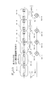
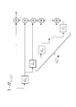
3.フィルタの縦続接続
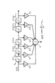
図1は、本実施の形態を実現するための一例として、ローパスフィルタを縦続接続したフィルタの一構成図である。
このフィルタは、ローパスフィルタLpk(z)をn個縦続接続したものである。ローパスフィルタLpk(z)は、基本となるローパスフィルタL0(z)をスケーリングした要素フィルタである。スケーリングとは、基本フィルタに対し、周波数軸又は時間軸上でpk+1倍にしたフィルタを定義したものである。
この図ではローパス型フィルタを基本構成とするスケーリングフィルタでのみ構成しているが、後で説明するように、ハイパスフィルタのみあるいはローパスフィルタとハイパスフィルタを混在した構成も本実施の形態を逸脱するものではない。
図14に、基本フィルタの縦続接続による周波数特性の変化の説明図を示す。
このように、上記スケーリングされたローパスフィルタLpk(z)を図1に示したように縦続接続することで、たとえば図14に示す周波数特性のフィルタを実現することができる。スケーリングしたフィルタを縦続接続することにより、通過帯域幅を狭めることが可能、阻止域を十分低下させることが可能、等の特徴が新たに見出される。
図中、1段は、基本フィルタL0の場合、2段は基本フィルタL0とフィルタL1を縦続接続した場合を示す。さらに、3段は、基本フィルタL0とフィルタL1とフィルタL2を縦続接続した場合を示す。このように、スケーリングしたフィルタの縦続接続により、通過帯域幅を狭めること、及び、阻止域を低下させることが可能となる。
上述の例はローパスフィルタのみで構成した例であるが、一般にはローパスフィルタとハイパスフィルタの組み合わせで、種々のフィルタX(z)を構成することが可能となる。すなわち、フィルタX(z)を一般的には次式で表すことができる。

L0は、ローパス基本フィルタ(マザーフィルタ)である。
H0は、ハイパス基本フィルタ(マザーフィルタ)である。
p,q は、スケーリング数(スケーリングファクタ)である。すなわち、周波数をp+1倍又はq+1倍にスケーリングしたフィルタを示す。
αpは、同一スケーリングフィルタの接続回数であり、p+1倍にスケーリングしたローパスフィルタの接続数(累乗値)である。
βqは、同一スケーリングフィルタの接続回数であり、q+1倍にスケーリングしたハイパスフィルタの接続数(累乗値)である。
X0(z)は目標の帯域幅(例えば、-3dB減衰までの周波数幅)を持つ最高次の
LP(z)=L0(zP+1)
または、
HQ(z)=H0(zQ+1)
で、その時の最高次数p、qをP,Qとする。
また、目標帯域幅fpとマザーフィルタL0,H0の帯域幅f0との関係は次式で表される。
fp=f0/(p+1)
以上のような、縦続接続による効果として、通過域においては、帯域幅を縮小させることができ、また、阻止域においては、不要な帯域を減衰させることができる。本実施の形態はこの特性を活かし、タップ数の少ないフィルタを構成することにある。
4.フィルタの構成方法
以下フィルタの構成方法について具体例を示す。
図15に、本実施の形態の帯域フィルタの説明図を示す。この図は、設計目標である実現するフィルタの特性を示す。
実現するフィルタの要求事項としては、下記の項目が与えられる。各記号の関係を図15に示す。
(1)標本化周波数fs
(2)中心周波数 fc
(3)遮断周波数(3dB減衰の周波数) f1、f-1
(4)通過域の周波数幅(-3dBバンド幅)Δfb
(5)阻止域の周波数 f2、f-2
(6)阻止域の減衰度 Ad(dB)
以下フィルタの構成方法について具体例を示す。
図15に、本実施の形態の帯域フィルタの説明図を示す。この図は、設計目標である実現するフィルタの特性を示す。
実現するフィルタの要求事項としては、下記の項目が与えられる。各記号の関係を図15に示す。
(1)標本化周波数fs
(2)中心周波数 fc
(3)遮断周波数(3dB減衰の周波数) f1、f-1
(4)通過域の周波数幅(-3dBバンド幅)Δfb
(5)阻止域の周波数 f2、f-2
(6)阻止域の減衰度 Ad(dB)
ここで、信号通過型フィルタの場合、標本化周波数fsとは、フィルタに入力される信号の繰り返し周波数で、中心周波数fcは信号に含まれる周波数成分の中から抽出するフィルタの中心の周波数であり、通常、ナイキストの定理から、fc/fs<0.5である。遮断周波数f1は信号を通過させる最大周波数であり、中心周波数fcを挟んで対象のf-1は信号を通過させる最少周波数である。ただし、ここでは、一例として、遮断周波数f1、f-1における通過信号の原信号に対する減衰度は-3dBとする。なお、-3dB以外にも適宜の値を基準として設定してもよい。この減衰度Aは入力信号の大きさをX、遮断周波数におけるフィルタ出力信号の大きさをYとするとき、下記式で定義される。

すなわち、遮断周波数f1、f-1では、入力信号の約70.8%(1/√2)に減衰された信号が出力されることを意味する。これは信号の振幅エネルギーが1/2に減衰することを表す。
この遮断周波数f1、f-1の間を信号通過域とし、その周波数幅Δfb(m)は、次式で与えられる。
Δfb(m)=f1-f-1=(f1-fc)*2
ここで、Δfb(m):m+1倍スケーリングしたフィルタの通過域幅
阻止周波数f2、f-2は入力信号のf2以上、あるいはf-2以下の周波数成分を阻止する周波数で、その時の減衰度Ad(例えば-80dB)を与えて、遮断周波数f1、f-1の減衰レベル(例えば-3dB)から減衰度Adまで減衰する遷移域の特性を与える。なお、-80dB以外にも、適宜の値を基準として設定してもよい。理想的には遮断周波数と阻止域周波数は同値であることが望ましいが、実際のフィルタにおいては実現困難のため、遷移域が存在する。阻止域の減衰度Adが-80dBとした時、入力信号Xとフィルタ出力信号の大きさの比は下記の様に、0.01%となる。
次に、上記の前提条件から、本実施の形態におけるフィルタの構成について説明する。
図16に、本実施の形態の帯域フィルタの周波数シフトの説明図を示す。
先ず、設計を簡単にするため、図16に示すように中心周波数fc(2πfc=ωc)の帯域通過型フィルタBB(z)を周波数0の点にシフトしたフィルタB(z)を考える。
すなわち、

と置くと、周波数推移定理より

となり、フィルタBB(z)は、フィルタB(z)の係数に2cos(ωck)を乗じた形に変換される。
このことから、まずは、要求事項を下記の事項に変換して、フィルタB(z)を設計すればよいことになる。
図16に、本実施の形態の帯域フィルタの周波数シフトの説明図を示す。
先ず、設計を簡単にするため、図16に示すように中心周波数fc(2πfc=ωc)の帯域通過型フィルタBB(z)を周波数0の点にシフトしたフィルタB(z)を考える。
すなわち、
このことから、まずは、要求事項を下記の事項に変換して、フィルタB(z)を設計すればよいことになる。
図21に、本実施の形態の帯域フィルタの説明図を示す。この図は、上述の設計目標である実現するフィルタの特性を示す。
(1)標本化周波数fs
(2)中心周波数 0
(3)遮断周波数(例:3dB減衰の周波数) fa=Δfb/2、-Δfb/2=-fa
(4)通過域の周波数幅(例:-3dBバンド幅)Δfb
(5)阻止域の周波数 fb=(f2-f-2)/2、-(f2-f-2)/2=-fb
(6)阻止域の減衰度 Ad(dB)(例:-80dB)
(1)標本化周波数fs
(2)中心周波数 0
(3)遮断周波数(例:3dB減衰の周波数) fa=Δfb/2、-Δfb/2=-fa
(4)通過域の周波数幅(例:-3dBバンド幅)Δfb
(5)阻止域の周波数 fb=(f2-f-2)/2、-(f2-f-2)/2=-fb
(6)阻止域の減衰度 Ad(dB)(例:-80dB)
次に、フィルタの縦続接続について説明する。
一般的には下記で表す。

ここで、
Lp(z)は、基本ローパスフィルタL0(z)をp+1倍スケーリングしたローパスフィルタである。
Hq(z)は、基本ハイパスフィルタH0(z)をq+1倍スケーリングしたハイパスフィルタである。
また、スケールファクターとして、最大スケール値Mは、通過域の周波数幅から決まるスケール値であり、P、Q(<M)はMよりも小さいスケール値を示す。また、αp、βqは同一のLp(z)、Hq(z)の累乗を示し、αp個、βq個縦続接続することを示す。
フィルタB0(z)は、ローパスフィルタの形式の場合はLM(z)であり、ハイパスフィルタの形式の場合はHM(z)である。
一般的には下記で表す。
Lp(z)は、基本ローパスフィルタL0(z)をp+1倍スケーリングしたローパスフィルタである。
Hq(z)は、基本ハイパスフィルタH0(z)をq+1倍スケーリングしたハイパスフィルタである。
また、スケールファクターとして、最大スケール値Mは、通過域の周波数幅から決まるスケール値であり、P、Q(<M)はMよりも小さいスケール値を示す。また、αp、βqは同一のLp(z)、Hq(z)の累乗を示し、αp個、βq個縦続接続することを示す。
フィルタB0(z)は、ローパスフィルタの形式の場合はLM(z)であり、ハイパスフィルタの形式の場合はHM(z)である。
図17に、本実施の形態の通過域周波数幅とスケーリングファクタの関係説明図を示す。
最大スケール値Mは要求される通過域の周波数幅Δfbから決定する。通過域の周波数幅Δfbは図13から明らかなように、スケール値が大きくなるほど狭くなることから、Δfbとスケール値p(またはq)との間には図17に示す関係がある。減衰度は、入力x(m)に対する出力Y(m)の減衰度を表し、Y(m)/x(m)=Lp(z)となるので、減衰度のデシベル(dB)の計算は、次のようになる。すなわち、この関係は、

を満足するΔfbとpとの関係であり、基本ローパスフィルタL0(z)の通過域幅Δfb0(=Δfb(0))と、p+1倍にスケーリングしたローパスフィルタの通過域幅Δfb(p)とは、下記関係で示すことができる。

本実施の形態では、一例として、p、q=MのローパスフィルタLM(z)あるいはハイパスフィルタHM(z)を初期値として、順次p、qを例えば降順で選択する等して、p、q、αp、βqの組み合わせの最適選択を行い、前記B(z)を設計していく。
Lp(z)、Hp(z)の選択は、阻止域周波数fbにおける減衰度が要求値Ad(例:-80dB)以下であるか否かで選択すると同時に、遮断周波数faにおける減衰度が要求値(例:-3dB)を大幅に下がるフィルタの場合は選択しない、という基準で選択する。
こうして、求めるフィルタBB(z)は下記となる。
ここで、フィルタLp(z)、Hq(z)に対して、各係数に2cos(ωck)を乗じることで、BB(z)を構成するLpB(z)、HqB(z)が求められる。
最大スケール値Mは要求される通過域の周波数幅Δfbから決定する。通過域の周波数幅Δfbは図13から明らかなように、スケール値が大きくなるほど狭くなることから、Δfbとスケール値p(またはq)との間には図17に示す関係がある。減衰度は、入力x(m)に対する出力Y(m)の減衰度を表し、Y(m)/x(m)=Lp(z)となるので、減衰度のデシベル(dB)の計算は、次のようになる。すなわち、この関係は、
Lp(z)、Hp(z)の選択は、阻止域周波数fbにおける減衰度が要求値Ad(例:-80dB)以下であるか否かで選択すると同時に、遮断周波数faにおける減衰度が要求値(例:-3dB)を大幅に下がるフィルタの場合は選択しない、という基準で選択する。
こうして、求めるフィルタBB(z)は下記となる。
図19は、本実施の形態による帯域フィルタの構成例を示す図である。
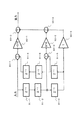
以上の方法で帯域フィルタは図に示す構成例で設計される。
このフィルタは、最大スケール値のフィルタB0(z)と、0B,…pBでスケーリングしたローパスフィルタL0B、…LpBをαp段縦続接続したフィルタと、0B,…qBでスケーリングしたハイパスフィルタH0B、…HqBをβq段接続したフィルタを備える。
以上の方法で帯域フィルタは図に示す構成例で設計される。
このフィルタは、最大スケール値のフィルタB0(z)と、0B,…pBでスケーリングしたローパスフィルタL0B、…LpBをαp段縦続接続したフィルタと、0B,…qBでスケーリングしたハイパスフィルタH0B、…HqBをβq段接続したフィルタを備える。
図20に、p+1倍にスケーリングしたローパスフィルタLpB(z)の構成図を示す。
このローパスフィルタは、p+1サンプル遅延する遅延素子201-1、201-2、201-3、201-4、201-5及び201-6と、乗算器202-1、202-2、202-3と、加算器203-1、203-2、203-3を備え、さらに、乗算器205-1、205-2、205-3を備える。乗算器202-1~202-3のフィルタ係数は、それぞれ-1/16、9/16、1である。また、乗算器205-1~205-3の係数は、それぞれ、2(1+cos(6ωc))、2(cos(2ωc)+cos(4ωc))、2cos(3ωc)である。なお、乗算器202-3は、係数が1なので、省略することができる。また、乗算器202-1と205-1、乗算器202-2と205-2、乗算器203-3と205-3をそれぞれ組み合わせたひとつの乗算器として構成してもよい。
このローパスフィルタは、p+1サンプル遅延する遅延素子201-1、201-2、201-3、201-4、201-5及び201-6と、乗算器202-1、202-2、202-3と、加算器203-1、203-2、203-3を備え、さらに、乗算器205-1、205-2、205-3を備える。乗算器202-1~202-3のフィルタ係数は、それぞれ-1/16、9/16、1である。また、乗算器205-1~205-3の係数は、それぞれ、2(1+cos(6ωc))、2(cos(2ωc)+cos(4ωc))、2cos(3ωc)である。なお、乗算器202-3は、係数が1なので、省略することができる。また、乗算器202-1と205-1、乗算器202-2と205-2、乗算器203-3と205-3をそれぞれ組み合わせたひとつの乗算器として構成してもよい。
図26に、q+1倍にスケーリングしたハイパスフィルタHqB(z)の構成図を示す。
このハイパスフィルタは、q+1サンプル遅延する遅延素子201-1、201-2、201-3、201-4、201-5及び201-6と、乗算器202-1、202-2、202-3と、加算器203-1、203-2、203-3を備え、さらに、乗算器205-1、205-2、205-3を備える。乗算器202-1~202-3のフィルタ係数は、それぞれ1/16、-9/16、1である。また、乗算器205-1~205-3の係数は、それぞれ、2(1+cos(6ωc))、2(cos(2ωc)+cos(4ωc))、2cos(3ωc)である。なお、乗算器202-3は、係数が1なので、省略することができる。また、乗算器202-1と205-1、乗算器202-2と205-2、乗算器203-3と205-3をそれぞれ組み合わせたひとつの乗算器として構成してもよい。
このハイパスフィルタは、q+1サンプル遅延する遅延素子201-1、201-2、201-3、201-4、201-5及び201-6と、乗算器202-1、202-2、202-3と、加算器203-1、203-2、203-3を備え、さらに、乗算器205-1、205-2、205-3を備える。乗算器202-1~202-3のフィルタ係数は、それぞれ1/16、-9/16、1である。また、乗算器205-1~205-3の係数は、それぞれ、2(1+cos(6ωc))、2(cos(2ωc)+cos(4ωc))、2cos(3ωc)である。なお、乗算器202-3は、係数が1なので、省略することができる。また、乗算器202-1と205-1、乗算器202-2と205-2、乗算器203-3と205-3をそれぞれ組み合わせたひとつの乗算器として構成してもよい。
5.フィルタ回路構成
以下に、他のフィルタ回路の構成について説明する。
図22に、基本ローパスフィルタL0B(z)の構成図を示す。
上式のような基本ローパスフィルタL0B(z)は、具体的には図示の回路構成で表される。
この基本ローパスフィルタは、1サンプル遅延する遅延素子21-1、21-2、21-3、21-4、21-5及び21-6と、乗算器22-1、22-2、22-3、22-4及び22-5と、加算器23-1、23-2、23-3及び23-4を備える。乗算器22-1~22-5のフィルタ係数は、それぞれ、-1/8、9/8cos(2ωc)、2cos(3ωc)、9/8cos(4ωc)、-1/8cos(6ωc)である。
以下に、他のフィルタ回路の構成について説明する。
図22に、基本ローパスフィルタL0B(z)の構成図を示す。
上式のような基本ローパスフィルタL0B(z)は、具体的には図示の回路構成で表される。
この基本ローパスフィルタは、1サンプル遅延する遅延素子21-1、21-2、21-3、21-4、21-5及び21-6と、乗算器22-1、22-2、22-3、22-4及び22-5と、加算器23-1、23-2、23-3及び23-4を備える。乗算器22-1~22-5のフィルタ係数は、それぞれ、-1/8、9/8cos(2ωc)、2cos(3ωc)、9/8cos(4ωc)、-1/8cos(6ωc)である。
図23に、p+1倍にスケーリングしたローパスフィルタLpB(z)の構成図を示す。
p+1倍にスケーリングしたローパスフィルタLpB(z)は、図示のように、L0Bと同様の構造であるが、Z-1がZ-(p+1)となる。
このp+1倍にスケーリングしたローパスフィルタは、p+1個の遅延素子を持つブロック31-1、31-2、31-3、31-4、31-5及び31-6と、乗算器32-1、32-2、32-3、32-4及び32-5と、加算器33-1、33-2、33-3及び33-4を備える。乗算器32-1~32-5のフィルタ係数は、それぞれ、-1/8、9/8cos(2ωc)、2cos(3ωc)、9/8cos(4ωc)、-1/8cos(6ωc)である。
また、例えば、この図では、各遅延素子31-1~31-6は(p+1)個の遅延素子を持つ。遅延素子の各ブロックは、(p+1)サンプル遅延する遅延素子であれば、個数はいくつでもよい。
図24に、基本ハイパスフィルタH0B(z)の構成図を示す。
また、このような基本ハイパスフィルタH0B(z)は、具体的には図示の回路構成で表される。
この基本ハイパスフィルタは、1サンプル遅延する遅延素子41-1、41-2、41-3、41-4、41-5及び41-6と、乗算器42-1、42-2、42-3、42-4及び42-5と、加算器43-1、43-2、43-3及び43-4を備える。乗算器42-1~42-5のフィルタ係数は、それぞれ、1/8、-9/8cos(2ωc)、2cos(3ωc)、-9/8cos(4ωc)、1/8cos(6ωc)である。
また、このような基本ハイパスフィルタH0B(z)は、具体的には図示の回路構成で表される。
この基本ハイパスフィルタは、1サンプル遅延する遅延素子41-1、41-2、41-3、41-4、41-5及び41-6と、乗算器42-1、42-2、42-3、42-4及び42-5と、加算器43-1、43-2、43-3及び43-4を備える。乗算器42-1~42-5のフィルタ係数は、それぞれ、1/8、-9/8cos(2ωc)、2cos(3ωc)、-9/8cos(4ωc)、1/8cos(6ωc)である。
図25に、q+1倍にスケーリングしたハイパスフィルタHqB(z)の構成図を示す。
q+1倍にスケーリングしたハイパスフィルタHqB(z)は、図示のように、H0と同様の構造であるが、Z-1がZ-(q+1)となる。
このq+1倍にスケーリングしたハイパスフィルタは、q+1個の遅延素子を持つブロック51-1、51-2、51-3、51-4、51-5及び51-6と、乗算器52-1、52-2、52-3、52-4及び52-5と、加算器53-1、53-2、53-3及び53-4を備える。乗算器52-1~52-5のフィルタ係数は、それぞれ、1/8、-9/8cos(2ωc)、2cos(3ωc)、-9/8cos(4ωc)、1/8cos(6ωc)である。
また、例えば、この図では、各遅延素子51-1~51-6は(q+1)個の遅延素子を持つ。遅延素子の各ブロックは、(q+1)サンプル遅延する遅延素子であれば、個数はいくつでもよい。
6.ハードウェア
図32は、本実施の形態に関する設計システムのハードウェアの構成図である。
この設計システムは、中央処理装置(CPU)である処理部1、入力部2、出力IF部3、表示部4及び記憶部5、フィルタ回路6を有する。また、処理部1、入力部2、出力IF部3、表示部4及び記憶部5は、スター又はバス等の適宜の接続手段で接続されている。
処理部1は、記憶部5にアクセスして、フィルタを設計する処理を実行する。
記憶部5は、設計仕様・要求事項(例えば、通過域及び阻止域についての条件(範囲、値、割合等)及びフィルタ縦続接続αp、βq数の上限等)を記憶するフィルタ構成ファイル51、前述のような基本ローパスフィルタ及びスケーリングしたローパスフィルタL0、L1、・・・、Lp、・・・、これらのフィルタLpの各フィルタ係数に2cos(ωck)を乗算したローパスフィルタLpB、基本ハイパスフィルタ及びスケーリングしたハイパスフィルタH0、H1、・・・、Hq、・・・、これらのフィルタHqの各フィルタ係数に2cos(ωck)を乗算したハイパスフィルタHqB、の各特性を記憶する基本フィルタ特性ファイル52、及び、設計されたフィルタ構成を定めるためのデータ・パラメータ(例えば、シフト量B、最大スケール値M、乗算器のフィルタ係数、p、q、αp、βp等)及び設計されたフィルタ特性等の処理部1による中間結果や最終結果等を記憶するフィルタ出力ファイル53を含む。これら各データは、処理部1により、出力IF部3を介して、フィルタ回路6(例えば、乗算器のフィルタ係数等、フィルタ構成を定めるためのデータ・パラメータ)に出力することができる。フィルタ回路6は、ソフトウェア又はハードウェアで構成され、処理部1により出力IF部3を介して、設定された各データに従い、所定の特性のフィルタを実現する。
7.設計フローチャート
図18は、本実施の形態の処理手順を示すフローチャートである。
設計システムは、以下のステップS01~S07により、フィルタを構成する。
図18は、本実施の形態の処理手順を示すフローチャートである。
設計システムは、以下のステップS01~S07により、フィルタを構成する。
(1)ステップS01
処理部1は、例えば、中心周波数fc、遮断周波数f1、阻止域周波数f2、通過域減衰度A、阻止域減衰度Ad,サンプル周波数fsを含む、設計仕様・要求事項となる所望の特性データを、入力部2からの操作に従い記憶部5(フィルタ構成ファイル51)に記憶することにより、又は、予め記憶された記憶部5(フィルタ構成ファイル51)に記憶された値を読み出すことにより、予め設定する。
処理部1は、例えば、中心周波数fc、遮断周波数f1、阻止域周波数f2、通過域減衰度A、阻止域減衰度Ad,サンプル周波数fsを含む、設計仕様・要求事項となる所望の特性データを、入力部2からの操作に従い記憶部5(フィルタ構成ファイル51)に記憶することにより、又は、予め記憶された記憶部5(フィルタ構成ファイル51)に記憶された値を読み出すことにより、予め設定する。
(2)ステップS03
処理部1は、ステップS01により、設定された特性データの各値を記憶部5(フィルタ構成ファイル51)から読み出し、入力された特性データに基づき、次式により、中心周波数fcを原点0にシフトするシフト量Bを算出する。
B=[fc/fs] ([ ]は、小数点四捨五入を示す。)
処理部1は、求めたシフト量Bを記憶部5(フィルタ出力ファイル53)に記憶する。
また、処理部1は、シフト量Bに従い、入力された特性データの中心周波数fc、遮断周波数f1、阻止域周波数f2をそれぞれ、中心周波数0、遮断周波数fa、阻止域周波数fbに変換し、各値を記憶部5(フィルタ出力ファイル53)に記憶する。
処理部1は、ステップS01により、設定された特性データの各値を記憶部5(フィルタ構成ファイル51)から読み出し、入力された特性データに基づき、最高次数のスケール値(スケーリングファクター)Mを算出する。
処理部は、最高次数のスケール値(最大スケール値)Mを、例えば、次のように、M+1倍にスケーリングしたフィルタの通過域幅Δfb(M)を算出する。
通過域幅Δfb(M)=(f1-fc)*2
次に、処理部1は、記憶部5(基本フィルタ特性ファイル52)に予め記憶されたスケーリング曲線を参照することにより、又は、そのスケーリング曲線の関係式から計算することにより、通過域幅Δfb(M)に従い最大スケール値Mを求める。
M=P=f-3(Δfb(M)) :-3dB値となるスケーリング曲線
=[Δfb(0)/Δfb(M)-1]: [ ]は小数点四捨五入
Δfb(0):基本フィルタの通過域幅
Δfb(M):M+1倍にスケーリングしたフィルタの通過域幅
なお、この例では、スケーリング曲線を-3dB値となる場合を示したが、これに限らず、遮断周波数又は通過域の周波数幅に対応して、適宜の値のスケーリング曲線を予め定めること又は処理部1が計算して設定することができる。
なお、処理部1は、最大スケール値Mを、入力部2又は記憶部5により、予め定められるようにしてもよい。
処理部1は、求めた最大スケール値Mを記憶部5(フィルタ出力ファイル53)に記憶する。
(3)ステップS05
処理部1は、ステップS01により設定された各値、及び、ステップS03により算出された最大スケール値Mを記憶部5(フィルタ構成ファイル51、フィルタ出力ファイル53)から読み出す。また、処理部1は、記憶部5から、次式のようなフィルタの組み合わせに基づき、p、q、αp,βqの組み合わせの最適選択を行う。
例えば、処理部1は、記憶部5(基本フィルタ特性ファイル52)からp,qで定められる該当するローパスフィルタLp及びハイパスフィルタHqの特性を読み出し、上式によりB(z)の特性を計算して求め、総当たりにより、設計仕様となる組合わせのうち、通過域および阻止域の設計仕様に合致するものを選択する。このとき、処理部1は、乗算器数が最少となるものをさらに選択するようにしてもよい。
Lp(z)、Hp(z)の選択は、阻止域周波数fbにおける減衰度が要求値Ad(例:-80dB)以下であるか否かで選択すると同時に、遮断周波数faにおける減衰度が要求値(例:-3dB)を大幅に下がるフィルタの場合は選択しない(例:予め定められた許容値以下のフィルタの場合は選択しない)、という基準で、処理部1は、p、q、αp,βqの組み合わせの最適選択を行う。
ここで、記憶部5(フィルタ構成ファイル51)等に、予めαp、βqの最大値を設定しておき、処理部1は、その最大値から例えば降順で選択して、また、p、qを最大スケール値Mから降順に選択して、p、q、αp、βqの組合わせの最適選択を行うことができる。
このとき、処理部は、次の判定及び処理を行うようにしてもよい。
(f=fs/(p+1)のXd=X(z)で最大減衰度を判定、
f=f2のXdが減少方向のとき、α、β増加
f=f1のXdが減少方向のとき、追加したLp、Hpを削除)
なお、上述では、基本ローパスフィルタ及び基本ハイパスフィルタをスケーリングしたフィルタの特性を記憶部5(基本フィルタ特性ファイル52)に予め記憶しておく例を説明したが、基本ローパスフィルタ及び基本ハイパスフィルタの特性のみを基本フィルタ特性ファイル52に記憶しておき、処理部1が必要に応じてこれら特性をもとにスケーリングの処理をして所定のスケーリングフィルタの特性を求めて用いるようにしてもよい。
処理部1は、求めたp、q、αp,βqを記憶部5(フィルタ出力ファイル53)に記憶する。
処理部1は、ステップS01により設定された各値、及び、ステップS03により算出された最大スケール値Mを記憶部5(フィルタ構成ファイル51、フィルタ出力ファイル53)から読み出す。また、処理部1は、記憶部5から、次式のようなフィルタの組み合わせに基づき、p、q、αp,βqの組み合わせの最適選択を行う。
Lp(z)、Hp(z)の選択は、阻止域周波数fbにおける減衰度が要求値Ad(例:-80dB)以下であるか否かで選択すると同時に、遮断周波数faにおける減衰度が要求値(例:-3dB)を大幅に下がるフィルタの場合は選択しない(例:予め定められた許容値以下のフィルタの場合は選択しない)、という基準で、処理部1は、p、q、αp,βqの組み合わせの最適選択を行う。
ここで、記憶部5(フィルタ構成ファイル51)等に、予めαp、βqの最大値を設定しておき、処理部1は、その最大値から例えば降順で選択して、また、p、qを最大スケール値Mから降順に選択して、p、q、αp、βqの組合わせの最適選択を行うことができる。
このとき、処理部は、次の判定及び処理を行うようにしてもよい。
(f=fs/(p+1)のXd=X(z)で最大減衰度を判定、
f=f2のXdが減少方向のとき、α、β増加
f=f1のXdが減少方向のとき、追加したLp、Hpを削除)
なお、上述では、基本ローパスフィルタ及び基本ハイパスフィルタをスケーリングしたフィルタの特性を記憶部5(基本フィルタ特性ファイル52)に予め記憶しておく例を説明したが、基本ローパスフィルタ及び基本ハイパスフィルタの特性のみを基本フィルタ特性ファイル52に記憶しておき、処理部1が必要に応じてこれら特性をもとにスケーリングの処理をして所定のスケーリングフィルタの特性を求めて用いるようにしてもよい。
処理部1は、求めたp、q、αp,βqを記憶部5(フィルタ出力ファイル53)に記憶する。
(4)ステップS07
処理部1は、記憶部5(フィルタ出力ファイル53)からp、q、αp,βq等のフィルタを構成するための仕様データ・パラメータを読み出し、さらに記憶部5(基本フィルタ特性ファイル52)から、ローパスフィルタ又はハイパスフィルタに従いB0(z)に相当するフィルタL0M又はフィルタH0Mの特性、また、フィルタLpB及びフィルタHqBの特性性を読み出し、次式に従いフィルタBB(z)を形成し、そのフィルタ特性及び使用データ・パラメータ等を表示部4に表示する及び/又は記憶部5(フィルタ出力ファイル53)に記憶する。
また、処理部1は、記憶部5(フィルタ出力ファイル53)からp、q、αp,βq等のフィルタを構成するための仕様データ・パラメータを読み出し、また、記憶部5(基本フィルタ特性ファイル52)から、フィルタLpB及びフィルタHqBの特性を読み出し、各値を出力IF部3を介してフィルタ回路6に出力することができる。そして、処理部1は、読み出した各値に従い、フィルタ回路6により、フィルタBB(z)を形成するようにしてもよい。フィルタ回路6は、フィルタBB(z)をコンピュータのシミュレーションで形成したり、ソフトウェアで形成することが出来る。また、フィルタ回路6は、出力IF部3から出力された各値に従い、ハードウェアでフィルタBB(z)を形成するようにしてもよい。
処理部1は、記憶部5(フィルタ出力ファイル53)からp、q、αp,βq等のフィルタを構成するための仕様データ・パラメータを読み出し、さらに記憶部5(基本フィルタ特性ファイル52)から、ローパスフィルタ又はハイパスフィルタに従いB0(z)に相当するフィルタL0M又はフィルタH0Mの特性、また、フィルタLpB及びフィルタHqBの特性性を読み出し、次式に従いフィルタBB(z)を形成し、そのフィルタ特性及び使用データ・パラメータ等を表示部4に表示する及び/又は記憶部5(フィルタ出力ファイル53)に記憶する。
8.係数の量子化展開方法
つぎに、フィルタ係数の量子化展開方法について説明する。
ここでいう量子化展開方法とは、上述のように設計された縦続接続構造のフィルタに基づき、そのインパルス応答特性と同じ特性を、図示のフィルタ回路構成で実現する方法である。
まず、Lp(z)=L0(zp+1)であることから、

で設計された縦続接続構造のフィルタにインパルス信号を入力してその応答を求める。インパルス応答については、例えば良く知られているMATLAB等のシミュレーションソフトで演算し、そのインパルス応答波形を求めることができる。あるいは、よく知られているMATHEMATHICA等の数式演算ソフトにより、上式のX(z)の展開式を導き出すことが可能である。その展開式は、X(z)のインパルス応答関数となっている。

従って、このインパルス応答の係数Ckをフィルター係数として用いて、フィルタを構成することができる。
つぎに、フィルタ係数の量子化展開方法について説明する。
ここでいう量子化展開方法とは、上述のように設計された縦続接続構造のフィルタに基づき、そのインパルス応答特性と同じ特性を、図示のフィルタ回路構成で実現する方法である。
まず、Lp(z)=L0(zp+1)であることから、
図27に、フィルタ構成図の一例を示す。
このフィルタは、乗算器72-0~72-k、1サンプル遅延する遅延素子71-1~k、加算器73-1~73-kを備える。
例えば、処理部1は、記憶部5(フィルタ出力ファイル53)からフィルタを構成するためのデータ(フィルタ係数、p、q、αp、βq等)を読み出し、フィルタ回路6などを用いて、インパルス応答を求め、そのインパルス応答の係数Ckを記憶部5(フィルタ出力ファイル53)に記憶する。
そして、処理部1は、フィルタ係数を記憶部5から読み出し、フィルタ回路6を用いることにより、
図示の回路構成において、上述の係数Ck(k+1個)をフィルタ係数(タップ係数)として用い、k個の遅延素子z-1を用いることで、フィルタを構成することができる。
図28に、他のフィルタ構成図の一例を示す。
このフィルタは、乗算器82-0~82-M、遅延素子81-1~M、加算器83を備える。
上述のフィルタ構成の他に、図示のようなフィルタ回路構成でも同様に、上述のように求めたフィルタ係数Ckにより設計された特性のフィルタを構成することができる。
このフィルタは、乗算器82-0~82-M、遅延素子81-1~M、加算器83を備える。
上述のフィルタ構成の他に、図示のようなフィルタ回路構成でも同様に、上述のように求めたフィルタ係数Ckにより設計された特性のフィルタを構成することができる。
9.本実施の形態と従来手法との比較検討
以下に、本実施の形態による手法と従来手法について比較する。
本実施の形態における要求仕様は次のとおりである。
標本化周波数 :1.8MHz
中心周波数 :450kHz
-3dB バンド幅 :6kHz
-80dB バンド幅:12kHz
量子化ビット数 :18-bit
位相特性 :線形位相
以下に、本実施の形態による手法と従来手法について比較する。
本実施の形態における要求仕様は次のとおりである。
標本化周波数 :1.8MHz
中心周波数 :450kHz
-3dB バンド幅 :6kHz
-80dB バンド幅:12kHz
量子化ビット数 :18-bit
位相特性 :線形位相
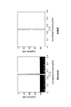
図29に、理論値における各手法により設計されたフィルタの周波数特性図を示す。
左図のとおり、Remez法では、仕様を満足するが、通過域及び阻止域にリップルが発生している。
一方、本発明によるフィルタでは、右図のとおり、仕様を満足し、阻止域での大きな減衰がみられる。
左図のとおり、Remez法では、仕様を満足するが、通過域及び阻止域にリップルが発生している。
一方、本発明によるフィルタでは、右図のとおり、仕様を満足し、阻止域での大きな減衰がみられる。
図30に、係数量子化後における各手法により設計されたフィルタの周波数特性図を示す。
左図のとおり、Remez法では、阻止域全体に亘り誤差が目立つ。
一方、本発明によるフィルタでは、右図のとおり、誤差は遷移域で若干程度みられるだけであることがわかる。
左図のとおり、Remez法では、阻止域全体に亘り誤差が目立つ。
一方、本発明によるフィルタでは、右図のとおり、誤差は遷移域で若干程度みられるだけであることがわかる。
図31に、要求仕様に対する本発明によるフィルタの評価を示す。
図示のとおり、本発明によるフィルタでは、従来手法と比較して非常に少ないタップ数で実現することができる。
図示のとおり、本発明によるフィルタでは、従来手法と比較して非常に少ないタップ数で実現することができる。
10.追記
本発明のフィルタの構成(設計)方法又はフィルタの構成(設計)装置・システムは、その各手順をコンピュータに実行させるためのフィルタの構成(設計)プログラム、フィルタの構成(設計)プログラムを記録したコンピュータ読み取り可能な記録媒体、フィルタの構成(設計)プログラムを含みコンピュータの内部メモリにロード可能なプログラム製品、そのプログラムを含むサーバ等のコンピュータ、等により提供されることができる。
本発明のフィルタの構成(設計)方法又はフィルタの構成(設計)装置・システムは、その各手順をコンピュータに実行させるためのフィルタの構成(設計)プログラム、フィルタの構成(設計)プログラムを記録したコンピュータ読み取り可能な記録媒体、フィルタの構成(設計)プログラムを含みコンピュータの内部メモリにロード可能なプログラム製品、そのプログラムを含むサーバ等のコンピュータ、等により提供されることができる。
11.フィルタGpass、Gstop、G
図33は、フィルタGの回路図を示す。
図34は、Gpassの回路図を示す。
図35及び図36に、Gpassの展開した図を示す。図35は、Gpassの前項部分を示す。図36は、Gpassの後項部分を示す。
上述のLm,Hmを用いて、以下の構成でフィルタの通過域主要部Gpassを形成する。
Gpassは、次式で表される。

ここで、Gpassの各添え字については以下の通り。
αP,βP :累乗値(同じLP,N1や[1-HP,N2]をαP回、βP回接続することを示す。ここで、記載の都合上、N1=Np (1),N2=Np (2) とした。)
NP (1) :Lp,N1においてHPのラダー接続の段数(図35の斜めの接続段数を示す。)
NP (2) :[1-Hp,N2]においてLPのラダー接続の段数(図36の斜めの接続段数を示す。)
P :周波数を(P+1)倍にスケーリングしたフィルタを示す。
スケーリングについては、次式の関係となる。
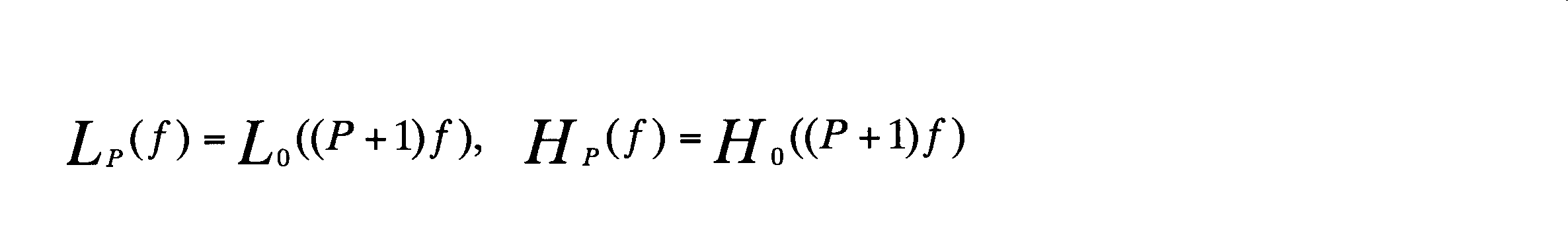
図33は、フィルタGの回路図を示す。
図34は、Gpassの回路図を示す。
図35及び図36に、Gpassの展開した図を示す。図35は、Gpassの前項部分を示す。図36は、Gpassの後項部分を示す。
上述のLm,Hmを用いて、以下の構成でフィルタの通過域主要部Gpassを形成する。
Gpassは、次式で表される。
αP,βP :累乗値(同じLP,N1や[1-HP,N2]をαP回、βP回接続することを示す。ここで、記載の都合上、N1=Np (1),N2=Np (2) とした。)
NP (1) :Lp,N1においてHPのラダー接続の段数(図35の斜めの接続段数を示す。)
NP (2) :[1-Hp,N2]においてLPのラダー接続の段数(図36の斜めの接続段数を示す。)
P :周波数を(P+1)倍にスケーリングしたフィルタを示す。
スケーリングについては、次式の関係となる。
図37は、Gstopの回路図を示す。
上述のLm,Hmを用いて、また、阻止域主要部Gstopも同様に形成する。
Gstopは、次式で表される。

αk,βl:累乗値(同じLpk,Nkや[1-Hql,Nl]をαk回、βl回接続することを示す。)
Nk :Lpk,NkにおいてHpのラダー接続の段数(図35の斜めの接続段数(Np (1)に相当)を示す。)
Nl :[1-Hql,Nl]においてLPのラダー接続の段数(図36の斜めの接続段数(Np (2)に相当)を示す。)
pk,ql:周波数をそれぞれ、(pk+1)、(ql+1)倍にスケーリングしたフィルタを示す。
ハイパスフィルタの各モジュールLpk,Nkおよび1-Hql,Nlの構造は、ローパスフィルタの各モジュール
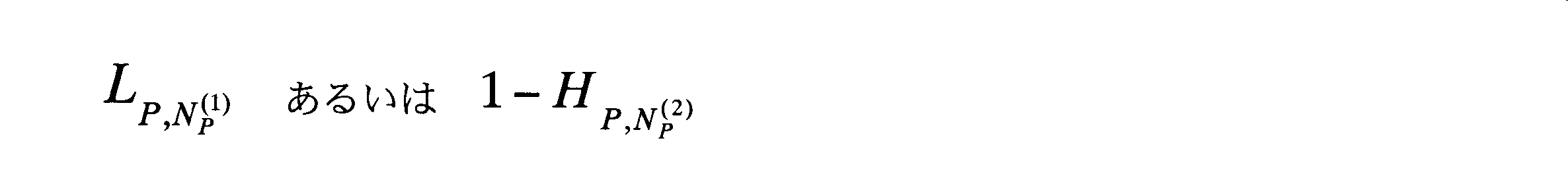
と同様である。
上述のLm,Hmを用いて、また、阻止域主要部Gstopも同様に形成する。
Gstopは、次式で表される。
Nk :Lpk,NkにおいてHpのラダー接続の段数(図35の斜めの接続段数(Np (1)に相当)を示す。)
Nl :[1-Hql,Nl]においてLPのラダー接続の段数(図36の斜めの接続段数(Np (2)に相当)を示す。)
pk,ql:周波数をそれぞれ、(pk+1)、(ql+1)倍にスケーリングしたフィルタを示す。
ハイパスフィルタの各モジュールLpk,Nkおよび1-Hql,Nlの構造は、ローパスフィルタの各モジュール
図38は、本実施の形態に関するハードウェアの構成図である。
このハードウェアは、中央処理装置(CPU)である処理部1、入力部2、出力IF部3、表示部4及び記憶部5、フィルタ回路6を有する。また、処理部1、入力部2、出力IF部3、表示部4及び記憶部5は、スター又はバス等の適宜の接続手段で接続されている。
記憶部5は、設計仕様・条件(例えば、通過域及び阻止域についての条件(範囲、値、割合等)及び乗算器数の上限Npass等)を記憶するフィルタ構成ファイル51、前述のような基本ローパスフィルタ及びスケーリングしたローパスフィルタ(L0、L1、・・・、Lm、・・・)、基本ハイパスフィルタ及びスケーリングしたハイパスフィルタ(H0、H1、・・・、Hm、・・・)の特性を記憶する基本フィルタ特性ファイル52、及び、設計されたフィルタ構成を定めるためのデータ・パラメータ(例えば、乗算器のフィルタ係数Npass、Np (1)、Np (2)αp、βp、P、Nk、Nl、αpk、βpl、pk、ql等)及び設計されたフィルタ特性等の処理部1による中間結果や最終結果等を記憶するフィルタ出力ファイル53を含む。これら各データは、処理部1により、出力IF部3を介して、フィルタ回路6(例えば、乗算器のフィルタ係数等、フィルタ構成を定めるためのデータ・パラメータ)に出力することができる。フィルタ回路6は、ソフトウェア又はハードウェアで構成され、処理部1により出力IF部3を介して、設定された各データに従い、所定の特性のフィルタを実現する。
12.フィルタ設計手順(ローパスフィルタ)
図39に、フィルタ設計手順(ローパスフィルタ)のフローチャートを示す。
このフローチャートは、以下の各ステップを含む。
0.設計仕様入力(S0)
1.最大スケール値p=Pの決定(S1)
2.通過域部Gpassの構成(S2)
3.阻止域部Gstopの構成(S3)
4.G=Gpass・Gstop(S4)
図39に、フィルタ設計手順(ローパスフィルタ)のフローチャートを示す。
このフローチャートは、以下の各ステップを含む。
0.設計仕様入力(S0)
1.最大スケール値p=Pの決定(S1)
2.通過域部Gpassの構成(S2)
3.阻止域部Gstopの構成(S3)
4.G=Gpass・Gstop(S4)
以下に、各ステップについて詳細に説明する。
0.設計仕様の設定(S0)
処理部1は、設計仕様(例えば、通過域及び阻止域についての条件(範囲、値、割合等)及び乗算器数の上限Npass等)を、入力部2からの操作に従い記憶部5(フィルタ構成ファイル51)に記憶することにより、又は、予め記憶された記憶部5(フィルタ構成ファイル51)に記憶された値を読み出すことにより、予め設定する。
0.設計仕様の設定(S0)
処理部1は、設計仕様(例えば、通過域及び阻止域についての条件(範囲、値、割合等)及び乗算器数の上限Npass等)を、入力部2からの操作に従い記憶部5(フィルタ構成ファイル51)に記憶することにより、又は、予め記憶された記憶部5(フィルタ構成ファイル51)に記憶された値を読み出すことにより、予め設定する。
図40に、積和モジュールの縦続接続モデルG(f)による遮断特性の図を示す。
図中、f3及びf80は次の通り。
f3:-3[dB]ラインとクロスする周波数(f=0から右に見て最初に-3[dB]ラインと交差する周波数点)
f80:-80[dB]ラインとクロスする周波数(f=fs/2から左に見て-80[dB]ラインと最初に交差する周波数点)
また、通過域と阻止域の周波数の比R(0<R≦1)を、 R=f3/f80 と定義する。
Rが1に近いほど、急峻さが高いことを意味する。急峻な遮断特性は、例えば、f3とf80の比を表した値R(0<R≦1)により、次式で表される。
R=f3/f80≒1
処理部1は、設計仕様を、例えば、以下のように設定することができる。
通過域 [0,f3]で-3[dB]以上
阻止域 [f80,1]で-80[dB]以下
R ≧R0(求めたフィルタの比Rが、予め定めた比R0以上であることを示す。)
ただし
0 <f3<f80<1,
0 <R0≦1
ステップS1.(pの最大値の決定)
処理部1は、ステップS1により、設定されたf3等の各値を記憶部5(フィルタ構成ファイル51)から読み出し、与えられたf3に合わせて最大スケール値p=Pを選択する。なお、処理部1は、Pの値を、入力部2又は記憶部5(フィルタ出力ファイル53)により、予め定められるようにしてもよい。
すなわち、処理部1は、f3 (p)をLpの-3[dB]点とし、f3 (0)は予め求めておき、そのとき
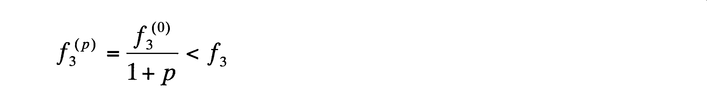
となる最小のpをPとする。
処理部1は、求めたPを記憶部5(フィルタ出力ファイル53)に記憶する。
処理部1は、ステップS1により、設定されたf3等の各値を記憶部5(フィルタ構成ファイル51)から読み出し、与えられたf3に合わせて最大スケール値p=Pを選択する。なお、処理部1は、Pの値を、入力部2又は記憶部5(フィルタ出力ファイル53)により、予め定められるようにしてもよい。
すなわち、処理部1は、f3 (p)をLpの-3[dB]点とし、f3 (0)は予め求めておき、そのとき
処理部1は、求めたPを記憶部5(フィルタ出力ファイル53)に記憶する。
ステップS2.通過域主要部の形成
処理部1は、ステップS1により設定されたNpass、R0等の各値を記憶部5(フィルタ構成ファイル51、フィルタ出力ファイル53)から読み出し、
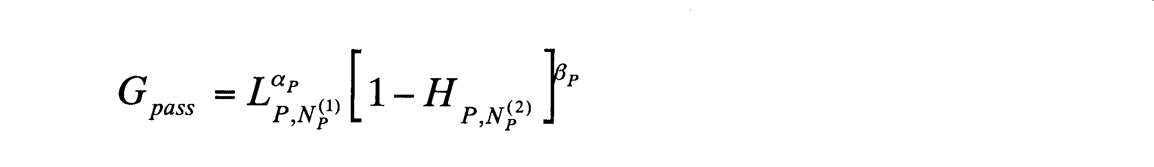
において設定した乗算器数の上限 Npass∈{1,2,・・・} を越えないように、
(Np (1),Np (2),αp,βp)⊂{0,1,2,・・・}
の総当たりにより、設計仕様(例:R≧R0)となる組合わせのうち、乗算器数が最少となるものを選択する。
例えば、処理部1は、記憶部5(基本フィルタ特性ファイル52)からNp (1),Np (2),αp,βpで定められる該当するローパスフィルタ及びハイパスフィルタの特性を読み出し、上式によりGpassの特性を計算して求め、総当たりにより、設計仕様(例:R≧R0)となる組合わせのうち、乗算器数が最少となるものを選択する。このとき、処理部1は、通過域および阻止域の設計仕様に合致するものをさらに選択するようにしてもよい。
ただし、組合せルールとして以下を定義する。
(αp,βp)≠(0,0),
Np (1)=0⇒αp=0,
Np (2)=0⇒βp=0
上述の乗算器数は、次のようになる。
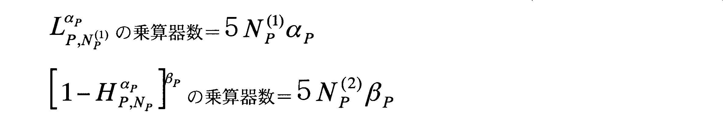
この場合、乗算器数には係数1の乗算器もカウントしているが、これを除くと、次式により乗算器数を上限Npass以下とする条件式が表される。
4(Np (1)αp+Np (2)βp)≦Npass
このようにして、処理部1は、求めたNp (1)、Np (2)、αp、βpを記憶部5(フィルタ出力ファイル53)に記憶する。
処理部1は、ステップS1により設定されたNpass、R0等の各値を記憶部5(フィルタ構成ファイル51、フィルタ出力ファイル53)から読み出し、
(Np (1),Np (2),αp,βp)⊂{0,1,2,・・・}
の総当たりにより、設計仕様(例:R≧R0)となる組合わせのうち、乗算器数が最少となるものを選択する。
例えば、処理部1は、記憶部5(基本フィルタ特性ファイル52)からNp (1),Np (2),αp,βpで定められる該当するローパスフィルタ及びハイパスフィルタの特性を読み出し、上式によりGpassの特性を計算して求め、総当たりにより、設計仕様(例:R≧R0)となる組合わせのうち、乗算器数が最少となるものを選択する。このとき、処理部1は、通過域および阻止域の設計仕様に合致するものをさらに選択するようにしてもよい。
ただし、組合せルールとして以下を定義する。
(αp,βp)≠(0,0),
Np (1)=0⇒αp=0,
Np (2)=0⇒βp=0
上述の乗算器数は、次のようになる。
4(Np (1)αp+Np (2)βp)≦Npass
このようにして、処理部1は、求めたNp (1)、Np (2)、αp、βpを記憶部5(フィルタ出力ファイル53)に記憶する。
ステップS3.阻止域部の形成
処理部1は、

において、
(Nk,Nl,αpk,βql)⊂{0,1,2,・・・}
の総当たりにより、
G=GpassGstop
を取って計算したとき、設計仕様(例:R≧R0)を保持している組合わせのうち、乗算器数が最少となるものを選択する。
例えば、処理部1は、記憶部5(基本フィルタ特性ファイル52)からNk,Nl,αpk,βqlで定められる該当するローパスフィルタ及びハイパスフィルタの特性を読み出し、上式によりGstopの特性を計算して求め、総当たりにより、
G=GpassGstop
を取って計算したとき、設計仕様(例:R≧R0)を保持している組合わせのうち、乗算器数が最少となるものを選択する。このとき、処理部1は、通過域および阻止域の設計仕様に合致するものをさらに選択するようにしてもよい。
処理部1は、求めたNk,Nl,αpk,βqlを記憶部5(フィルタ出力ファイル53)に記憶する。
処理部1は、
(Nk,Nl,αpk,βql)⊂{0,1,2,・・・}
の総当たりにより、
G=GpassGstop
を取って計算したとき、設計仕様(例:R≧R0)を保持している組合わせのうち、乗算器数が最少となるものを選択する。
例えば、処理部1は、記憶部5(基本フィルタ特性ファイル52)からNk,Nl,αpk,βqlで定められる該当するローパスフィルタ及びハイパスフィルタの特性を読み出し、上式によりGstopの特性を計算して求め、総当たりにより、
G=GpassGstop
を取って計算したとき、設計仕様(例:R≧R0)を保持している組合わせのうち、乗算器数が最少となるものを選択する。このとき、処理部1は、通過域および阻止域の設計仕様に合致するものをさらに選択するようにしてもよい。
処理部1は、求めたNk,Nl,αpk,βqlを記憶部5(フィルタ出力ファイル53)に記憶する。
ステップS4.Gの構成及び出力
処理部1は、記憶部5(フィルタ出力ファイル53)からNp (1),Np (2),αp,βp,Nk,Nl,αpk,βpl等のフィルタを構成するための仕様データ・パラメータを読み出し、さらに記憶部5(基本フィルタ特性ファイル52)から基本ローパスフィルタとそのスケーリングしたフィルタ、基本ハイパスフィルタとそのスケーリングしたフィルタの特性を読み出し、Gpass及びGstopを上述の各式に従い形成し、G=GpassGstopに従いフィルタGを形成し、そのフィルタGの特性を表示部4に表示する及び/又は記憶部5(フィルタ出力ファイル53)に記憶する。
また、処理部1は、記憶部5(フィルタ出力ファイル53)からNp (1),Np (2),αp,βp,Nk,Nl,αpk,βpl等のフィルタを構成するための仕様データ・パラメータを読み出し、各値を出力IF部3を介してフィルタ回路6に出力する。そして、処理部1は、読み出した各値に従い、フィルタ回路6により、Gpass及びGstopを上述の各式に従い形成し、G=GpassGstopに従いフィルタGを形成するようにしてもよい。フィルタ回路6は、フィルタGをコンピュータのシミュレーションで形成したり、ソフトウェアで形成することが出来る。また、フィルタ回路6は、出力IF部3から出力された各値に従い、ハードウェアでフィルタGを形成するようにしてもよい。
なお、上述では、基本ローパスフィルタ及び基本ハイパスフィルタをスケーリングしたフィルタの特性を記憶部5(基本フィルタ特性ファイル52)に予め記憶しておく例を説明したが、基本ローパスフィルタ及び基本ハイパスフィルタの特性のみを基本フィルタ特性ファイル52に記憶しておき、処理部1が必要に応じてこれら特性をもとにスケーリングの処理をして所定のスケーリングフィルタの特性を求めて用いるようにしてもよい。
13.ローパスフィルタの設計例
(1)基本的な特性改善
図45に、G(f)により特性が改善される例(ローパスフィルタ)の説明図を示す。
この図は、ローパスフィルタL0(f)とL1(f)を縦続接続することにより、次式のフィルタG(f)を形成し、そのフィルタGの特性を示したものである。
G(f)=L0(f)L1(f)
このように、要素となるフィルタを縦続接続することにより、急峻な特性に改善することができる。
(1)基本的な特性改善
図45に、G(f)により特性が改善される例(ローパスフィルタ)の説明図を示す。
この図は、ローパスフィルタL0(f)とL1(f)を縦続接続することにより、次式のフィルタG(f)を形成し、そのフィルタGの特性を示したものである。
G(f)=L0(f)L1(f)
このように、要素となるフィルタを縦続接続することにより、急峻な特性に改善することができる。
(2)フローチャートによる設計例
図41は、ローパスフィルタ仕様の説明図である。
ここでは、上述の構成手段に従い、ローパスフィルタの構成例を与える。所望の特性の仕様は、図示の通りとする。通過域、阻止域は正規化した周波数での区間である。
本実施の形態のフローチャートで設計したフィルタの構成式は次の通りである:
G=L3 7,9L1 3,1L1 4,2L1 5,3(1-H1 1,1)(1-H1 2,1)
この例では、P=7を選択し、その上でα7=0,1,2,3,4およびN7=0,1,2,3,・・・等をトライアルし、Gpass=L3 7,9と設定した。
図41は、ローパスフィルタ仕様の説明図である。
ここでは、上述の構成手段に従い、ローパスフィルタの構成例を与える。所望の特性の仕様は、図示の通りとする。通過域、阻止域は正規化した周波数での区間である。
本実施の形態のフローチャートで設計したフィルタの構成式は次の通りである:
G=L3 7,9L1 3,1L1 4,2L1 5,3(1-H1 1,1)(1-H1 2,1)
この例では、P=7を選択し、その上でα7=0,1,2,3,4およびN7=0,1,2,3,・・・等をトライアルし、Gpass=L3 7,9と設定した。
図42は、Gpass及びGstop、フィルタGの説明図である。
図42(a)に、Gpassの特性図を示す。Gpassの特性は、通過域区間=[0,0.096]、阻止域区間=[0.013,1]、およびR=0.738、乗算器数=150個となっている。
次に阻止域については、Gpassの第2~4サイドローブを阻止しなくてはならないが、第3、第4サイドローブについては図26(b)中の(1-H1 1,1)および(1-H1 2,1)によりほぼ阻止される。ここでは、P≦5を取ることにし、図26(b)から分かるように、第2サイドローブ中心付近はL1 3,1とL1 4,2により、右側付近はL1 3,1と1-H1 2,1により阻止されている。左側付近を阻止するために、p=5に対し、N5=0,1,2,・・・およびα5=0,1,2等をトライアルし、乗算器数との兼合いで(α5,N5)=(1,3)を選択した。
図43に、従来法および本発明で構成したフィルタの特性図を示す。(a)は最小2乗法、(b)はRemez法、(c)は、本発明による方法である。
図44は、各設計法での乗算器数及びRの比較を示す図である。ここで乗算器数は、特性が最初に仕様を完全に満たすようになったときのものである。本発明による方法は、最小2乗法に比べると乗算器数、Rともに優っている。Remez法はRは本発明による方法よりも僅かに優っているが、乗算器数が1142と多い。Remez法に対する優位性の確認を補足するため、Remez法のR=0.762を超えるR値(ここでは=0.767)となったときの乗算器数をみると365であった。
この結果により、本発明による積和モジュールによる要素フィルタの縦続接続による急峻なローパスフィルタ特性近似モデルの有効性が示された。
この結果により、本発明による積和モジュールによる要素フィルタの縦続接続による急峻なローパスフィルタ特性近似モデルの有効性が示された。
上述には、インパルス応答関数としては、例えば、、区分的m次多項式を用いることができ、また、波形調整パラメータ付き補間関数等を用いてもよい。
本発明は、音響技術、映像技術、画像技術、伝送技術、通信技術、アナログデジタル変換・デジタルアナログ変換技術、圧縮・解凍技術、暗号・解読(解凍)技術、フィルタ技術等、様々な技術に適用することができる。
本発明は、音響、画像、通信、などにおける信号処理のフィルタとして広範囲に利用可能である。
また、本発明は、例えば、アンプ等の音響装置、動画、静止画処理のための画像装置、携帯電話等の通信装置、制御装置、コンピュータ、PC等の様々な各種装置に用いることができる。
本発明は、音響技術、映像技術、画像技術、伝送技術、通信技術、アナログデジタル変換・デジタルアナログ変換技術、圧縮・解凍技術、暗号・解読(解凍)技術、フィルタ技術等、様々な技術に適用することができる。
本発明は、音響、画像、通信、などにおける信号処理のフィルタとして広範囲に利用可能である。
また、本発明は、例えば、アンプ等の音響装置、動画、静止画処理のための画像装置、携帯電話等の通信装置、制御装置、コンピュータ、PC等の様々な各種装置に用いることができる。
Claims (15)
- 有限台の区分的多項式で構成されるインパルス応答函数の節点値を係数とする低域通過/高域通過型の基本フィルタを構成し、該基本フィルタを時間軸あるいは周波数軸でスケーリングした複数のスケーリングフィルタを組み合わせて所望の特性とすることを特徴とするフィルタ。
- 請求項1で各スケーリングフィルタを縦続構造で組み合わせることを特徴とするフィルタ。
- 請求項1及び2において、有限区間の離散入力に係数を乗じて遅延させた信号を順次加算する構成を基本構成とし、その基本構成における遅延素子の数を増減してスケーリングフィルタを構成し、該スケーリングフィルタを縦続接続して信号を出力することを特徴とするフィルタ。
- 有限台の区分的多項式で構成されるインパルス応答函数の節点値を係数とする低域通過/高域通過型の基本フィルタを構成し、該基本フィルタを時間軸あるいは周波数軸でスケーリングした複数のスケーリングフィルタを組み合わせて所望の特性とすることを特徴とするFIRフィルタにおいて、中心周波数、遮断周波数、阻止域周波数、阻止域最高減衰度およびサンプリング周波数を入力し、遮断周波数と中心周波数と決定される通過域周波数幅からスケーリングの最大次数を決定し、該スケーリング次数より少ない次数のスケーリングフィルタを順次選択して、求めるFIRフィルタの阻止域周波数における減衰度が所定の前記最大減衰度以下となるように選択したスケーリングフィルタの採否を判定し、スケーリングフィルタを縦続接続で構成することを特徴とするフィルタ。
- 請求項4において、フィルタ係数を量子化し、該量子化した係数による通過域周波数幅、遮断周波数における減衰度、阻止域減衰度を再計算し、量子化による前記各値の誤差が許容範囲内となる様に、スケーリングフィルタの組み合わせを増減することを特徴とするフィルタ。
- 請求項4において、スケーリングの最大次数は基本フィルタの通過域周波数幅と求めるフィルタの通過域周波数幅との比から決定することを特徴とするフィルタ。
- 請求項4において、阻止域減衰度は、サンプリング周波数と(スケーリングファクタ+1)との比で決まる周波数におけるフィルタゲインを阻止域最高減衰度として求めることを特徴とするフィルタ。
- 請求項4において、スケーリングフィルタの選択において、組み合わせ前後におけるフィルタの阻止域周波数におけるフィルタゲインが減少方向のとき、同じスケーリングフィルタを縦続接続させる構成とすることを特徴とするフィルタ。
- 請求項1において、サンプリング周波数と所望の中心周波数との比で求まる遅延素子数分だけ、入力信号を遅延させて前記フィルタの入力とすることでバンドパスフィルタとすることを特徴とするフィルタ。
- 請求項1において、複数のスケーリングフィルタは次数の高くなる順序で順次構成することを特徴とするフィルタ。
- 請求項1において、前記低域通過型フィルタ及び高域通過型フィルタを周波数スケーリングしたスケーリングフィルタを、通過帯域幅が所定の要求幅以上となる様に選択し、該選択されたスケーリングフィルタを用いて、通過域特性を所定の要求特性となるように構成した通過域フィルタと、阻止域特性を所定の要求特性となるように構成した阻止域フィルタとを縦続構成で形成することを特徴とするフィルタ。
- 請求項1において、、前記低域通過型フィルタ及び高域通過型フィルタを周波数スケーリングしたスケーリングフィルタを、通過帯域幅が所定の要求幅以上となる様に選択し、該選択されたスケーリングフィルタを用いて、要求特性を満足する低域通過型のスケーリングフィルタを選定し、該選定された低域通過型のスケーリングフィルタに対して、高域通過型のスケーリングフィルタをラダー状に接続することにより、フィルタの通過域特性を形成することを特徴とするフィルタ。
- 請求項1において、前記低域通過型フィルタ及び高域通過型フィルタを周波数スケーリングしたスケーリングフィルタを、通過帯域幅が所定の要求幅以上となる様に選択し、該選択されたスケーリングフィルタを用いて、要求特性を満足する高域通過型のスケーリングフィルタを選定し、該選定された高域通過型のスケーリングフィルタに対して、低域通過型のスケーリングフィルタをラダー状に接続することにより、フィルタの通過域特性を形成することを特徴とするフィルタ。
- 請求項11乃至請求項13に記載されたフィルタに対し、阻止域の特性を要求特性とする補正フィルタを前記スケーリングフィルタにより構成し、該補正フィルタを前記通過域特性フィルタに縦続接続するように構成することを特徴とするフィルタ。
- 請求項1乃至14において、所定の通過帯域幅を満足するスケーリングの最大次数として、最大スケール値Pを、次式となる最小のpをPとすることを特徴とするフィルタ。
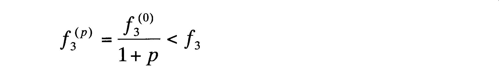
f3:-3[dB]ラインとクロスする周波数(設計仕様で与えられる。)
f3 (0):Lpの-3[dB]点(予め設定される。)
f3 (p):Lpの-3[dB]点
Priority Applications (2)
| Application Number | Priority Date | Filing Date | Title |
|---|---|---|---|
| EP09762379.7A EP2315353B1 (en) | 2008-06-10 | 2009-06-01 | Filter |
| US12/997,233 US8949303B2 (en) | 2008-06-10 | 2009-06-01 | Filter |
Applications Claiming Priority (4)
| Application Number | Priority Date | Filing Date | Title |
|---|---|---|---|
| JP2008-151982 | 2008-06-10 | ||
| JP2008151982A JP4968850B2 (ja) | 2008-06-10 | 2008-06-10 | フィルタ、フィルタの設計システム及び設計方法及び設計プログラム |
| JP2008200907A JP2010041311A (ja) | 2008-08-04 | 2008-08-04 | フィルタ、フィルタの構成システム及び構成方法 |
| JP2008-200907 | 2008-08-04 |
Publications (1)
| Publication Number | Publication Date |
|---|---|
| WO2009150949A1 true WO2009150949A1 (ja) | 2009-12-17 |
Family
ID=41416660
Family Applications (1)
| Application Number | Title | Priority Date | Filing Date |
|---|---|---|---|
| PCT/JP2009/059953 WO2009150949A1 (ja) | 2008-06-10 | 2009-06-01 | フィルタ |
Country Status (3)
| Country | Link |
|---|---|
| US (1) | US8949303B2 (ja) |
| EP (1) | EP2315353B1 (ja) |
| WO (1) | WO2009150949A1 (ja) |
Families Citing this family (5)
| Publication number | Priority date | Publication date | Assignee | Title |
|---|---|---|---|---|
| US8953716B1 (en) * | 2011-09-14 | 2015-02-10 | Marvell International Ltd. | DC offset estimation and compensaton for wideband systems |
| CN103684348A (zh) * | 2013-12-31 | 2014-03-26 | 中国人民解放军国防科学技术大学 | 基于二阶iir低通滤波器的去乘快速算法 |
| TWI571052B (zh) * | 2015-09-30 | 2017-02-11 | 國立彰化師範大學 | 串接式有限脈衝響應濾波器及其訊號處理方法 |
| US11517248B2 (en) * | 2016-03-04 | 2022-12-06 | University Of Tennessee Research Foundation | Ambulatory seizure monitoring system and method |
| CN107979712B (zh) * | 2016-10-20 | 2020-02-21 | 上海富瀚微电子股份有限公司 | 一种视频降噪方法及装置 |
Citations (7)
| Publication number | Priority date | Publication date | Assignee | Title |
|---|---|---|---|---|
| JPS63269613A (ja) * | 1987-04-28 | 1988-11-07 | Kenwood Corp | デジタル・フイルタ |
| JPH02222319A (ja) * | 1989-02-23 | 1990-09-05 | Lsi Rojitsuku Kk | ディジタルフィルタ |
| JPH06503450A (ja) * | 1990-12-19 | 1994-04-14 | ルンナー,トマス | 積の数を減らすことによりディジタルフィルタバンクの電力消費を減らす方法 |
| JP2001084242A (ja) | 1999-09-10 | 2001-03-30 | Hitachi Ltd | 可変演算プロセッサ |
| JP2001102931A (ja) | 1999-09-27 | 2001-04-13 | Japan Science & Technology Corp | フィルタバンク及びフィルタリング方法 |
| WO2004008637A1 (ja) * | 2002-07-15 | 2004-01-22 | Neuro Solution Corp. | デジタルフィルタの設計方法、デジタルフィルタ設計用プログラム、デジタルフィルタ |
| JP2006020191A (ja) | 2004-07-05 | 2006-01-19 | Nec Corp | Firフィルタ |
Family Cites Families (11)
| Publication number | Priority date | Publication date | Assignee | Title |
|---|---|---|---|---|
| JPH0770957B2 (ja) | 1988-04-26 | 1995-07-31 | パイオニア株式会社 | Firフィルタ |
| US5212659A (en) | 1991-10-08 | 1993-05-18 | Crystal Semiconductor | Low precision finite impulse response filter for digital interpolation |
| JP4023842B2 (ja) | 1995-09-28 | 2007-12-19 | ソニー株式会社 | ディジタルフィルタ及び音響再生装置 |
| US6748409B1 (en) * | 1998-01-26 | 2004-06-08 | Niigata Seimitsu Co., Ltd. | Data interpolating system |
| JP4397488B2 (ja) * | 1999-12-17 | 2010-01-13 | Nsc株式会社 | オーバーサンプリング処理回路およびデジタル−アナログ変換器 |
| JP4300272B2 (ja) * | 2001-09-10 | 2009-07-22 | Nsc株式会社 | デジタルフィルタおよびその設計方法 |
| US20050120067A1 (en) * | 2002-07-15 | 2005-06-02 | Neuro Solution Corp. | Digital filter designing method, digital filter designing program, digital filter |
| US7529788B2 (en) * | 2002-10-21 | 2009-05-05 | Neuro Solution Corp. | Digital filter design method and device, digital filter design program, and digital filter |
| TW200414675A (en) | 2002-10-21 | 2004-08-01 | Neuro Solution Corp | Digital filter design method and device, digital filter design program, and digital filter |
| GB2427093A (en) | 2004-02-17 | 2006-12-13 | Neuro Solution Corp | Digital filter design method and device, digital filter design program, and digital filter |
| TW200740113A (en) * | 2006-03-07 | 2007-10-16 | Neuro Solution Corp | Interpolation function generation circuit |
-
2009
- 2009-06-01 US US12/997,233 patent/US8949303B2/en active Active
- 2009-06-01 WO PCT/JP2009/059953 patent/WO2009150949A1/ja active Application Filing
- 2009-06-01 EP EP09762379.7A patent/EP2315353B1/en active Active
Patent Citations (7)
| Publication number | Priority date | Publication date | Assignee | Title |
|---|---|---|---|---|
| JPS63269613A (ja) * | 1987-04-28 | 1988-11-07 | Kenwood Corp | デジタル・フイルタ |
| JPH02222319A (ja) * | 1989-02-23 | 1990-09-05 | Lsi Rojitsuku Kk | ディジタルフィルタ |
| JPH06503450A (ja) * | 1990-12-19 | 1994-04-14 | ルンナー,トマス | 積の数を減らすことによりディジタルフィルタバンクの電力消費を減らす方法 |
| JP2001084242A (ja) | 1999-09-10 | 2001-03-30 | Hitachi Ltd | 可変演算プロセッサ |
| JP2001102931A (ja) | 1999-09-27 | 2001-04-13 | Japan Science & Technology Corp | フィルタバンク及びフィルタリング方法 |
| WO2004008637A1 (ja) * | 2002-07-15 | 2004-01-22 | Neuro Solution Corp. | デジタルフィルタの設計方法、デジタルフィルタ設計用プログラム、デジタルフィルタ |
| JP2006020191A (ja) | 2004-07-05 | 2006-01-19 | Nec Corp | Firフィルタ |
Non-Patent Citations (5)
Also Published As
| Publication number | Publication date |
|---|---|
| EP2315353A1 (en) | 2011-04-27 |
| EP2315353A4 (en) | 2013-07-03 |
| US20110153704A1 (en) | 2011-06-23 |
| US8949303B2 (en) | 2015-02-03 |
| EP2315353B1 (en) | 2020-07-29 |
Similar Documents
| Publication | Publication Date | Title |
|---|---|---|
| JP3337722B2 (ja) | デジタル・インターポレータ | |
| EP2200180B1 (en) | Subband signal processing | |
| JP2002374150A (ja) | デジタルフィルタ及びデジタル信号のフィルタリング方法 | |
| US11263293B2 (en) | Digital sample rate conversion | |
| US7196648B1 (en) | Non-integer decimation using cascaded intergrator-comb filter | |
| US7324025B1 (en) | Non-integer interpolation using cascaded integrator-comb filter | |
| WO2009150949A1 (ja) | フィルタ | |
| US7529788B2 (en) | Digital filter design method and device, digital filter design program, and digital filter | |
| US7280878B1 (en) | Sample rate converter having distributed filtering | |
| JP2010041311A (ja) | フィルタ、フィルタの構成システム及び構成方法 | |
| JP4300272B2 (ja) | デジタルフィルタおよびその設計方法 | |
| JPH08508374A (ja) | デシメーション・フィルター | |
| US8645443B2 (en) | Desensitized filters with droop correction | |
| JP2004120182A (ja) | デシメーションフィルタおよびインターポレーションフィルタ | |
| US7774394B2 (en) | Exponentiated polyphase digital filter | |
| JP4968850B2 (ja) | フィルタ、フィルタの設計システム及び設計方法及び設計プログラム | |
| US7242326B1 (en) | Sample rate conversion combined with filter | |
| WO2004079905A1 (ja) | デジタルフィルタの設計方法および装置、デジタルフィルタ設計用プログラム、デジタルフィルタ | |
| JP2002043965A (ja) | 受信機 | |
| Awasthi et al. | Compensated CIC-hybrid signed digit decimation filter | |
| Mottaghi-Kashtiban et al. | FIR filters involving shifts and only two additions, efficient for short word-length signal processing | |
| JPWO2007102611A1 (ja) | 補間関数生成回路 | |
| JP4989575B2 (ja) | フィルタ及びフィルタの構成方法 | |
| US10943330B2 (en) | Image processing filter | |
| US7262717B2 (en) | Sample rate conversion combined with filter |
Legal Events
| Date | Code | Title | Description |
|---|---|---|---|
| 121 | Ep: the epo has been informed by wipo that ep was designated in this application |
Ref document number: 09762379 Country of ref document: EP Kind code of ref document: A1 |
|
| WWE | Wipo information: entry into national phase |
Ref document number: 2009762379 Country of ref document: EP |
|
| NENP | Non-entry into the national phase |
Ref country code: DE |
|
| WWE | Wipo information: entry into national phase |
Ref document number: 12997233 Country of ref document: US |