WO2009139258A1 - 光学素子、アーム機構、および情報記録装置 - Google Patents
光学素子、アーム機構、および情報記録装置 Download PDFInfo
- Publication number
- WO2009139258A1 WO2009139258A1 PCT/JP2009/057576 JP2009057576W WO2009139258A1 WO 2009139258 A1 WO2009139258 A1 WO 2009139258A1 JP 2009057576 W JP2009057576 W JP 2009057576W WO 2009139258 A1 WO2009139258 A1 WO 2009139258A1
- Authority
- WO
- WIPO (PCT)
- Prior art keywords
- optical element
- light
- diffraction grating
- arm
- waveguide
- Prior art date
Links
Images


Classifications
-
- G—PHYSICS
- G11—INFORMATION STORAGE
- G11B—INFORMATION STORAGE BASED ON RELATIVE MOVEMENT BETWEEN RECORD CARRIER AND TRANSDUCER
- G11B5/00—Recording by magnetisation or demagnetisation of a record carrier; Reproducing by magnetic means; Record carriers therefor
- G11B5/127—Structure or manufacture of heads, e.g. inductive
- G11B5/31—Structure or manufacture of heads, e.g. inductive using thin films
- G11B5/3109—Details
- G11B5/313—Disposition of layers
- G11B5/3133—Disposition of layers including layers not usually being a part of the electromagnetic transducer structure and providing additional features, e.g. for improving heat radiation, reduction of power dissipation, adaptations for measurement or indication of gap depth or other properties of the structure
- G11B5/314—Disposition of layers including layers not usually being a part of the electromagnetic transducer structure and providing additional features, e.g. for improving heat radiation, reduction of power dissipation, adaptations for measurement or indication of gap depth or other properties of the structure where the layers are extra layers normally not provided in the transducing structure, e.g. optical layers
-
- G—PHYSICS
- G11—INFORMATION STORAGE
- G11B—INFORMATION STORAGE BASED ON RELATIVE MOVEMENT BETWEEN RECORD CARRIER AND TRANSDUCER
- G11B5/00—Recording by magnetisation or demagnetisation of a record carrier; Reproducing by magnetic means; Record carriers therefor
- G11B5/48—Disposition or mounting of heads or head supports relative to record carriers ; arrangements of heads, e.g. for scanning the record carrier to increase the relative speed
- G11B5/4806—Disposition or mounting of heads or head supports relative to record carriers ; arrangements of heads, e.g. for scanning the record carrier to increase the relative speed specially adapted for disk drive assemblies, e.g. assembly prior to operation, hard or flexible disk drives
- G11B5/4833—Structure of the arm assembly, e.g. load beams, flexures, parts of the arm adapted for controlling vertical force on the head
-
- G—PHYSICS
- G11—INFORMATION STORAGE
- G11B—INFORMATION STORAGE BASED ON RELATIVE MOVEMENT BETWEEN RECORD CARRIER AND TRANSDUCER
- G11B5/00—Recording by magnetisation or demagnetisation of a record carrier; Reproducing by magnetic means; Record carriers therefor
- G11B5/48—Disposition or mounting of heads or head supports relative to record carriers ; arrangements of heads, e.g. for scanning the record carrier to increase the relative speed
- G11B5/4806—Disposition or mounting of heads or head supports relative to record carriers ; arrangements of heads, e.g. for scanning the record carrier to increase the relative speed specially adapted for disk drive assemblies, e.g. assembly prior to operation, hard or flexible disk drives
- G11B5/4866—Disposition or mounting of heads or head supports relative to record carriers ; arrangements of heads, e.g. for scanning the record carrier to increase the relative speed specially adapted for disk drive assemblies, e.g. assembly prior to operation, hard or flexible disk drives the arm comprising an optical waveguide, e.g. for thermally-assisted recording
-
- G—PHYSICS
- G11—INFORMATION STORAGE
- G11B—INFORMATION STORAGE BASED ON RELATIVE MOVEMENT BETWEEN RECORD CARRIER AND TRANSDUCER
- G11B5/00—Recording by magnetisation or demagnetisation of a record carrier; Reproducing by magnetic means; Record carriers therefor
- G11B2005/0002—Special dispositions or recording techniques
- G11B2005/0005—Arrangements, methods or circuits
- G11B2005/0021—Thermally assisted recording using an auxiliary energy source for heating the recording layer locally to assist the magnetization reversal
Definitions
- the present invention relates to an information recording apparatus, and an arm mechanism and an optical element used therefor, for example, an optically assisted magnetic recording apparatus that uses a magnetic field and light for information recording, and an arm mechanism and an optical element used therefor It is about.
- the PSIM proposed in Patent Document 1 is provided with a diffraction grating, and considering the ratio of the amount of light collected by the PSIM with respect to the amount of light irradiated to the diffraction grating (light utilization efficiency),
- the incident angle to the diffraction grating has an appropriate angle range with respect to the wavelength of incident light.
- the present invention has been made in view of the above-described problems, and an object of the present invention is to propose a light guide technology to a waveguide that increases the light utilization efficiency.
- an arm mechanism includes an arm part, a head part including a waveguide provided with a grating coupler and attached to one end side of the arm part, and the grating coupler. And an optical element that is disposed on the optical path of the incident light and is attached to the arm portion and has a diffraction grating.
- the arm mechanism according to the second aspect is the arm mechanism according to the first aspect, wherein the optical element includes a prism.
- the arm mechanism according to the third aspect is the arm mechanism according to the first or second aspect, wherein the optical element has at least one reflecting surface.
- An arm mechanism is the arm mechanism according to the third aspect, wherein the diffraction grating is formed by a plurality of reflecting surfaces, and a light diffraction phenomenon is caused by reflection of light by the plurality of reflecting surfaces. Includes the resulting diffraction grating.
- An information recording apparatus includes an arm mechanism according to any one of the first to fourth aspects, a light source unit that generates light to be applied to the head unit via the optical element, A recording medium disposed opposite to the head unit, and the head unit records information on the recording medium by irradiating the recording medium with light.
- An optical element according to a sixth aspect is an optical element disposed on an optical path of light incident on a grating coupler provided in a waveguide, and is an optical element of the grating coupler according to a wavelength variation of light.
- a diffraction grating is provided that changes the direction in which light is emitted so as to correspond to fluctuations in the appropriate incident angle.
- the optical element according to the seventh aspect is the optical element according to the sixth aspect and includes a prism.
- the optical element according to the eighth aspect is the optical element according to the sixth or seventh aspect, and has at least one reflecting surface.
- the appropriate range of the incident angle of light with respect to the grating coupler changes according to the change in the wavelength of the light. Since the incident angle with respect to the grating coupler is adjusted by the optical element provided on the optical path, the light utilization efficiency can be increased.
- the optical path can be adjusted by the diffraction grating of the optical element following the change in the range of the appropriate incident angle with respect to the grating coupler.
- the information recording apparatus of the fifth aspect it is possible to reduce power consumption in recording information.
- FIG. 1 is a diagram showing a schematic configuration example of an information recording apparatus according to an embodiment of the present invention.
- FIG. 2 is a diagram illustrating a configuration example of the slider unit according to the embodiment of the present invention.
- FIG. 3 is a diagram illustrating a configuration example of an optical assist unit having a waveguide.
- FIG. 4 is a schematic diagram illustrating a configuration example of the arm mechanism.
- FIG. 5 is a diagram illustrating an arrangement of optical elements.
- FIG. 6 is a diagram illustrating characteristics of the first to fifth light source units.
- FIG. 7 is a diagram illustrating characteristics of the first to fifth light source units.
- FIG. 8 is a schematic cross-sectional view showing a configuration example of a waveguide grating element.
- FIG. 1 is a diagram showing a schematic configuration example of an information recording apparatus according to an embodiment of the present invention.
- FIG. 2 is a diagram illustrating a configuration example of the slider unit according to the embodiment of the present invention.
- FIG. 3 is
- FIG. 9 is a diagram for explaining chromatic dispersion characteristics related to the waveguide.
- FIG. 10 is a schematic view illustrating fluctuations in the appropriate incident angle to the waveguide.
- FIG. 11 is a diagram illustrating the relationship between the incident efficiency to the waveguide and the incident angle to the waveguide.
- FIG. 12 is a schematic diagram illustrating a configuration example of the first optical element unit.
- FIG. 13 is a diagram for explaining the adjustment of the incident angle by the first optical element unit.
- FIG. 14 is a schematic diagram illustrating a configuration example of an optical element unit according to a modification.
- FIG. 1 is a diagram illustrating a schematic configuration example of the information recording apparatus 100.
- three orthogonal XYZ axes are appropriately attached in order to clarify the orientation relationship.
- an information recording apparatus 100 is an optically assisted magnetic recording head, that is, a magnetic recording apparatus equipped with first to fifth slider portions 31 to 35 corresponding to the optical head (optically assisted magnetic recording apparatus).
- a magnetic recording apparatus equipped with first to fifth slider portions 31 to 35 corresponding to the optical head (optically assisted magnetic recording apparatus).
- the information recording apparatus 100 includes a substantially rectangular parallelepiped casing 1, first to third recording disks (magnetic recording media) 2a, 2b, 2c and an arm mechanism 10 disposed in the casing 1. Yes.
- the first to third recording disks 2a, 2b, and 2c are disk-shaped recording media, and are arranged so as to be separated from each other by a predetermined minute distance (for example, 1 mm or less) so that the disk surfaces are substantially parallel to each other. .
- the first recording disk 2a, the second recording disk 2b, and the third recording disk 2c are arranged sequentially in this order from the top (from the + Z side to the -Z side).
- the body 1 is rotatably supported by a predetermined rotating shaft and a motor.
- the arm mechanism 10 mainly includes first to fifth slider portions 31 to 35, first to fifth optical element portions 21 to 25, first to third arm portions 41 to 43, and a rotating shaft 5.
- the first to third arm portions 41 to 43 have the same shape, and each have a thin plate shape and an elongated shape, and are arranged substantially parallel to each other. Specifically, the first arm part 41, the second arm part 42, and the third arm part 43 are sequentially arranged in this order from above (from the + Z side to the -Z side).
- the first to third arm portions 41 to 43 are connected to each other by a rotating shaft 5 on one end side (here, the end portion in the ⁇ X direction), and in the direction of the arrow mA with the rotating shaft 5 as a fulcrum. It is supported so as to be rotatable with respect to the housing 1 in the tracking direction.
- the first to third arm portions 41 to 43 rotate in the arrow mA direction with the rotary shaft 5 as a fulcrum.
- the first arm part 41 and the second arm part 42 are arranged so as to sandwich the first recording disk 2a, and the second arm part 42 and the third arm part 43 hold the second recording disk 2b. It is arranged so as to sandwich it. From another point of view, the second arm part 42 is arranged so as to be sandwiched between the first recording disk 2a and the second recording disk 2b, and the third arm part 43 is arranged with the second recording disk 2b. It is arranged so as to be sandwiched between the third recording disk 2c.
- the first to fifth slider portions 31 to 35 have the same configuration, and are optical heads (corresponding to the “head portion” of the present invention) for irradiating the recording disks 2a, 2b, and 2c with light. is there.
- the first slider portion 31 has one main surface (first main surface) of the first recording disc 2a with respect to the lower surface on the other end side different from the one end side to which the rotary shaft 5 of the first arm portion 41 is connected.
- the second slider portion 32 is provided so as to face the upper surface), and the second slider portion 32 has the second arm portion 42 with respect to the upper surface on the other end side different from the one end side to which the rotating shaft 5 is coupled. It is provided so as to face the other main surface (here, the lower surface) of one recording disk 2a.
- the third slider portion 33 has one main surface of the second recording disk 2b (with respect to the lower surface on the other end side different from the one end side to which the rotating shaft 5 of the second arm portion 42 is coupled).
- the fourth slider portion 34 is arranged to face the upper surface on the other end side different from the one end side to which the rotating shaft 5 of the third arm portion 43 is connected. 2 is provided so as to face the other main surface (here, the lower surface) of the recording disk 2b. Further, the fifth slider portion 35 has one main surface of the third recording disk 2c (with respect to the lower surface on the other end side different from the one end side to which the rotating shaft 5 of the third arm portion 43 is connected). Here, it is provided so as to face the upper surface). As described above, the first to fifth slider portions 31 to 35 are held by the first to third arm portions 41 to 43.
- the shape of the surface (slider lower surface) facing each recording disk 2a to 2c in each of the slider portions 31 to 35 is a so-called air bearing surface shape (ABS: Air Bearing Surface).
- ABS Air Bearing Surface
- a motor (not shown) for rotating the first to third recording disks 2a to 2c in the direction of the arrow mB is provided in the housing 1. Then, when the first to third recording disks 2a to 2c are rotated, the first to fifth slider portions 31 to 35 are moved on the first to third recording disks 2a, 2b, and 2c.
- the disk 2a, 2b, 2c is configured to be able to move relatively while being levitated by a substantially constant distance.
- FIG. 2 is a schematic cross-sectional view showing a configuration example of the first to fifth slider portions 31 to 35.
- the first to fifth slider portions 31 to 35 have recording heads that use light for information recording on the first to third recording disks 2a to 2c.
- the first to fifth slider portions 31 to 35 are each composed of a substrate 50 made of, for example, ceramic. Inside the substrate 50, there are recorded portions of the first to third recording disks 2a to 2c.
- an optical assist unit 51, a magnetic recording unit 52, and a magnetic reproducing unit 53 are formed.
- the light assist portion 51 is mainly configured to have an optical waveguide, and the optical waveguide is provided to hang from the side surface of the substrate 50 to the lower surface.
- a metal film in which a minute rectangular opening is formed is disposed at an end (outgoing end) for emitting light in the optical waveguide. For this reason, the light incident from the end (incident end) opposite to the exit end of the optical waveguide is guided from the side surface side to the lower surface side of the substrate 50.
- an optical waveguide has a taper part for condensing with respect to an output end.
- the structure of the optical waveguide has a waveguide 60 (see FIG. 3) described later.
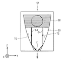
- FIG. 3 is a diagram illustrating a configuration example of the optical assist unit 51 having the waveguide 60.
- the waveguide 60 for example, a waveguide type solid immersion mirror (PSIM) proposed in Patent Document 1 can be applied.
- PSD waveguide type solid immersion mirror
- the waveguide 60 has parabolic inner surfaces 70 and 72 that are thin and have a width that gradually decreases from the top to the bottom. Further, a grating coupler corresponding to an optical coupler having a diffraction grating portion 68 is provided on the upper side surface of the waveguide 60.
- the laser light is irradiated on the diffraction grating portion 68 (specifically, the laser irradiation region in the thick broken line portion) and the laser light is introduced into the waveguide 60, the laser light is emitted as indicated by the thick arrow 64. Reflected by the inner surfaces 70 and 72, the laser beam is condensed at the lowermost focal point F of the waveguide 60, and electromagnetic waves are generated toward the first to third recording disks 2a to 2c. A small area of the disks 2a to 2c is heated. In FIG. 2, the outer edge of the optical path PR of the laser light applied to the light assist unit 51 is illustrated by a one-dot chain line. In consideration of increasing the incident efficiency of the laser light with respect to the waveguide 60, an appropriate angle (appropriate incident angle) exists for the incident angle of the laser light with respect to the diffraction grating portion 68. This proper incident angle will be described later.
- the magnetic recording section 52 is formed of a magnetic recording element that writes magnetic information to the recording portions of the first to third recording disks 2a to 2c.
- the sliders 31 to 35 record information by the magnetic recording unit 52 while irradiating the recording disks 2a to 2c with light by the light assist unit 51.
- first to fifth light source portions P1 to P5 (see FIG. 4) for supplying light beams are arranged for the first to fifth slider portions 31 to 35, respectively.
- the first to fifth light source parts P1 to P5 are constituted by, for example, a semiconductor laser chip or the like, and are appropriately attached to the arm parts 41 to 43.
- the magnetic reproducing unit 53 is formed by a magnetic reproducing element that reads magnetic information recorded on the first to third recording disks 2a to 2c.
- the first to fifth optical element portions 21 to 25 have the same configuration, have diffraction gratings, and are attached to the first to third arm portions 41 to 43.
- Each optical element portion 21 to 25 is in the vicinity of each slider portion 31 to 35 and on each optical path of light emitted from each light source portion P1 to P5 (FIG. 4) and incident on each diffraction grating portion 68. Placed in.
- the first optical element portion 21 is on the rotating shaft 5 side of the first slider portion 31 and the other end different from the one end side to which the rotating shaft 5 of the first arm portion 41 is connected.
- the second optical element portion 22 is located on the rotating shaft 5 side of the second slider portion 32, and is connected to the one end side to which the rotating shaft 5 of the second arm portion 42 is connected. Are provided on the upper surface on the other end side.
- the third optical element portion 23 is on the rotating shaft 5 side of the third slider portion 33, and the lower surface on the other end side different from the one end side to which the rotating shaft 5 of the second arm portion 42 is connected.
- the fourth optical element portion 24 is on the rotating shaft 5 side of the fourth slider portion 34 and is different from the one end side to which the rotating shaft 5 of the third arm portion 43 is connected. It is provided with respect to the upper surface of the end side. Further, the fifth optical element portion 25 is on the rotating shaft 5 side of the fifth slider portion 35, and the lower surface on the other end side is different from the one end side to which the rotating shaft 5 of the third arm portion 43 is connected. Is provided against. Thus, the first to fifth optical element portions 21 to 25 are held by the first to third arm portions 41 to 43.
- FIG. 4 is a schematic diagram illustrating a configuration example of the arm mechanism 10.
- FIG. 4 is a schematic view of the configuration of the arm mechanism 10 and its periphery viewed from above (+ Z direction).
- the first to fifth light source units P1 to P5 and the first to fifth optical element units 21 to 25 are shown.
- the arrangement relationship of the first to fifth slider portions 31 to 35 with respect to the first arm portion 41 is schematically shown by broken lines.
- optical paths L1 to L5 of light emitted from the light source parts P1 to P5 and introduced into the slider parts 31 to 35 via the optical element parts 21 to 25 are indicated by alternate long and short dash lines.
- FIG. 5 is a schematic view illustrating the arrangement of the optical element portion 21.
- the optical path L1 of the laser light from the first light source portion P1 to the first slider portion 31 is indicated by a one-dot chain line. .
- the first arm portion 41 includes an arm main body portion 41a and a suspension portion 41b.
- the arm body 41a is made of a material that is thicker and more rigid than the suspension 41b, and the suspension 41b is made of a flexible material.
- the arm body 41a and the suspension The extending direction of 41b is substantially the same.
- One end ( ⁇ X side end) of the arm main body 41a is fixed to the rotating shaft 5, and the suspension is placed on the lower surface ( ⁇ Z side surface) of the other end (+ X side end) of the arm main body 41a.
- the upper surface (the surface on the + Z side) at one end of the portion 41b is connected.
- the first slider portion 31 and the first optical element portion 21 are attached to the lower surface near the other end opposite to the one end connected to the arm main body portion 41a of the suspension portion 41b. . Specifically, the first slider portion 31 is attached to the suspension portion 41b via a predetermined spring member, and the first optical element portion 21 is attached to the suspension portion 41b with a resin adhesive or the like. ing. Further, the first light source P1 is disposed on the lower surface (the surface on the ⁇ Z side) near one end (the end on the ⁇ X side) fixed to the rotating shaft 5 of the arm main body 41a. Light emitted from P ⁇ b> 1 is supplied to the first slider portion 31 through the first optical element portion 21. In other words, the first optical element unit 21 is disposed between the first light source unit P1 and the first slider unit 31, and the first optical path of the laser light from the first light source unit P1 to the first slider unit 31 is first. An optical element unit 21 is disposed.
- the second arm portion 42 includes an arm main body portion 42a, an upper suspension portion 42b, and a lower suspension portion 42c that have substantially the same extending direction. Then, one end ( ⁇ X side end) of the arm main body 42a is fixed to the rotating shaft 5, and the upper suspension is placed on the upper surface (+ Z side surface) of the other end (+ X side end) of the arm main body 42a. The lower surface of one end of the portion 42b (the surface on the ⁇ Z side) is coupled, and the lower surface (the surface on the ⁇ Z side) of the other end of the arm main body portion 42a (the surface on the ⁇ Z side) is connected to the upper surface of one end of the lower suspension portion 42c ( + Z side surfaces) are connected.
- the second slider part 32 and the second optical element part 22 are attached to the upper surface of the upper suspension part 42b near the other end opposite to one end connected to the arm body part 42a. ing. Specifically, the second slider part 32 is attached to the upper suspension part 42b via a predetermined spring member, and the second optical element part 22 is attached to the upper suspension part 42b by a resin adhesive or the like. It is attached.
- the second light source P2 is arranged on the upper surface (+ Z side surface) near one end ( ⁇ X side end) fixed to the rotation shaft 5 of the arm main body 42a. The light emitted from the second slider portion 32 is supplied to the second slider portion 32 via the second optical element portion 22.
- the second optical element unit 22 is disposed between the second light source unit P2 and the second slider unit 32, and the second optical element unit 22 is arranged on the optical path of the laser light from the second light source unit P2 to the second slider unit 32.
- An optical element unit 22 is disposed.
- the third slider portion 33 and the third optical element portion 23 are attached to the lower surface in the vicinity of the other end opposite to the one end connected to the arm main body portion 42a of the lower suspension portion 42c. Yes. Specifically, the third slider portion 33 is attached to the lower suspension portion 42c via a predetermined spring member, and the third optical element portion 23 is attached to the lower suspension portion 42c by a resin adhesive or the like. It is attached.
- the third light source P3 is disposed on the lower surface (the surface on the ⁇ Z side) near one end (the end on the ⁇ X side) fixed to the rotating shaft 5 of the arm main body 42a. The light emitted from P3 is supplied to the third slider portion 33 via the third optical element portion 23.
- the third optical element unit 23 is disposed between the third light source unit P3 and the third slider unit 33, and the third optical path of the laser light from the third light source unit P3 to the third slider unit 33 is third.
- An optical element unit 23 is disposed.
- the third arm portion 43 includes an arm main body portion 43a, an upper suspension portion 43b, and a lower suspension portion 43c.
- the extending directions of the arm main body portion 43a, the upper suspension portion 43b, and the lower suspension portion 43c are substantially the same. is there.
- One end ( ⁇ X side end) of the arm main body 43a is fixed to the rotary shaft 5, and the upper suspension is placed on the upper surface (+ Z side surface) of the other end (+ X side end) of the arm main body 43a.
- the lower surface of one end of the portion 43b (the surface on the ⁇ Z side) is connected, and the upper surface of one end of the lower suspension portion 43c (the surface on the ⁇ Z side) is connected to the lower surface (the surface on the ⁇ Z side) of the other end of the arm main body portion 43a. + Z side surfaces) are connected.
- the fourth slider part 34 and the fourth optical element part 24 are attached to the upper surface of the upper suspension part 43b near the other end opposite to the one end connected to the arm body part 43a. ing. Specifically, the fourth slider portion 34 is attached to the upper suspension portion 43b via a predetermined spring member, and the fourth optical element portion 24 is attached to the upper suspension portion 43b by a resin adhesive or the like. It is attached.
- the fourth light source P4 is disposed on the upper surface (+ Z side surface) near one end ( ⁇ X side end) fixed to the rotation shaft 5 of the arm main body 43a, and the fourth light source unit P4. The light emitted from the first slider is supplied to the fourth slider portion 34 via the fourth optical element portion 24.
- the fourth optical element unit 24 is disposed between the fourth light source unit P4 and the fourth slider unit 34, and the fourth optical path of the laser light from the fourth light source unit P4 to the fourth slider unit 34 is fourth.
- An optical element unit 24 is disposed.
- the fifth slider portion 35 and the fifth optical element portion 25 are attached to the lower surface in the vicinity of the other end opposite to the one end connected to the arm main body portion 43a of the lower suspension portion 43c. Yes. Specifically, the fifth slider part 35 is attached to the lower suspension part 43c via a predetermined spring member, and the fifth optical element part 25 is attached to the lower suspension part 43c by a resin adhesive or the like. It is attached.
- the fifth light source P5 is disposed on the lower surface (the surface on the ⁇ Z side) near one end (the end on the ⁇ X side) fixed to the rotation shaft 5 of the arm main body 43a. The light emitted from P5 is supplied to the fifth slider portion 35 via the fifth optical element portion 25.
- the fifth optical element unit 25 is disposed between the fifth light source unit P5 and the fifth slider unit 35, and the fifth optical element path 25 extends from the fifth light source unit P5 to the fifth slider unit 35.
- An optical element unit 25 is disposed.
- the first to fifth light source sections P1 to P5 generate light that irradiates the first to fifth slider sections 31 to 35 through the first to fifth optical element sections 21 to 25, respectively. It is composed of inexpensive Fabry-Perot type laser diodes used in typical CD players and DVD recorders.
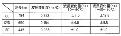
- FIG. 6 and 7 are diagrams illustrating characteristics of the first to fifth light source parts P1 to P5.
- FIG. 6 shows the characteristics of laser light sources used in general CD players, DVD recorders, and Blu-ray disc (BD) recorders.
- the wavelength of the laser light at room temperature (25 ° C.) the degree of change of the wavelength with respect to the temperature variation of the laser light source (wavelength change degree), a predetermined temperature range of the wavelength ( A change amount (wavelength change amount) at 0 to 60 ° C. and a change amount (wavelength change amount) of the wavelength in a predetermined temperature range ( ⁇ 40 to 70 ° C.) are shown.
- FIG. 7 is a diagram illustrating the temperature dependence of the wavelength of laser light emitted from a laser light source used in a general CD player.
- each laser light source When each laser light source emits laser light continuously or intermittently, it generates heat and the temperature of the laser light source rises, so that the wavelength of the laser light emitted from the laser light source varies. As shown in FIGS. 6 and 7, the fluctuation amount of the wavelength is as large as about ⁇ 7 nm, for example, even in a normal use environment (temperature range: 0 to 60 ° C.). Due to this variation in wavelength, the appropriate incident angle of the laser beam with respect to the diffraction grating portion 68 varies. Therefore, in the information recording apparatus 100 according to the present embodiment, the first to fifth optical element units 21 to 25 are provided in order to compensate for fluctuations in the appropriate incident angle.
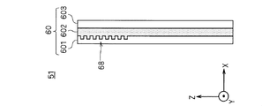
- FIG. 8 is a schematic cross-sectional view illustrating the configuration of an element (waveguide grating element) of the waveguide 60 in which the diffraction grating portion 68 is provided.
- the waveguide 60 is formed by laminating a lower clad layer 603, a core layer 602, and an upper clad layer 601 in this order.
- a diffraction grating portion 68 for optical coupling is provided on the core layer 602 sandwiched between the upper cladding layer 601 and the lower cladding layer 603.
- the core layer 602 is formed of a material having a higher refractive index than the cladding layers 601 and 603, and the light applied to the diffraction grating portion 68 is coupled by the diffraction grating portion 68, propagates through the core layer 602, and below ( In FIG. 8, the process proceeds in the ⁇ Z direction.
- FIG. 9 is a diagram for explaining the wavelength dispersion characteristic (wavelength dispersion characteristic) of the waveguide 60.
- wavelength dispersion characteristic wavelength dispersion characteristic
- the propagation constant of the waveguide mode in the core layer 602 is ⁇ 0
- the angle formed by the light beam radiated outside the waveguide 60 with respect to the XY plane (radiation angle to the outside of the substrate) is ⁇ 0
- the refractive index in the upper cladding layer 601 is n c
- the refractive index in the core layer 602 is n f
- the effective refractive index of the waveguide mode in the core layer 602 (also referred to as an equivalent refractive index or effective refractive index) is N
- the diffraction grating portion If the period of 68 irregularities is ⁇ , the wavelength of light emitted outside the waveguide 60 is ⁇ , and the order of diffraction is q (here, only ⁇ 1), the following equation (1) is established.
- the refractive index n 0 of the air which constitutes an external waveguide 60 is 1.0
- the refractive index n c of the SiO 2 which is a material of the upper cladding layer 601 is 1.47
- the refractive index n f of 2 O 5 is 2.1
- the effective refractive index N is 1.72
- the period ⁇ is 0.8462 ⁇ m
- the wavelength ⁇ is 785 nm
- the radiation angle ⁇ to the outside of the substrate from the above equation (1) 0 becomes 52.4 °.
- the appropriate incident angle of the light beam with the wavelength ⁇ with respect to the diffraction grating portion 68 is 52. 4 °.
- the appropriate incident angle indicates an appropriate value of the angle formed by incident light with respect to the XY plane (incident angle at which the incident efficiency is maximized). As shown in FIGS. 6 and 7, when the wavelength ⁇ varies by about ⁇ 7 nm, the proper incident angle varies by about ⁇ 0.78 °.
- the appropriate incident angle to the waveguide 60 from the outside of the waveguide 60 can be determined from the effective refractive index N of the waveguide mode in the core layer 602, the period ⁇ of the diffraction grating portion 68, and the like. .
- the proper angle of incidence also depends on the wavelength of the light (incident light) incident to the waveguide 60 lambda, the proper angle of incidence theta 11 becomes the time of the wavelength lambda 1, appropriate for when the wavelength is lambda 2 incident angle is ⁇ 12.
- the appropriate incident angle ⁇ 11 and the appropriate incident angle ⁇ 12 are expressed by the following equation (3). Have a relationship.
- the period ⁇ of the diffraction grating portion 68 is preferably set to a period at which secondary light and tertiary light are generated in consideration of the coupling efficiency of light, for example, 0.5 to 5 times the wavelength ⁇ . It is preferable to set the degree. However, under such conditions, the incident angle of the incident light with respect to the waveguide 60 is preferably within ⁇ 0.1 ° from the appropriate incident angle.
- FIG. 11 illustrates the relationship between the incident efficiency corresponding to the ratio of the amount of light incident on the waveguide 60 (incident light amount) to the amount of light irradiated on the waveguide 60 (irradiation light amount) and the incident angle of the incident light on the waveguide 60. It is a figure to do.
- FIG. 11 shows the case where the proper incident angle is 52.4 ° as described above, the horizontal axis indicates the incident angle, and the vertical axis indicates the incident efficiency when the maximum value of the incident efficiency is 1. Relative efficiency).
- the incident angle of the incident light with respect to the waveguide 60 is ⁇ 0.1 ° centered on the appropriate incident angle of 52.4 °. Need to be set within.
- the temperatures of the first to fifth light source portions P1 to P5 are set as described above.
- the wavelength ⁇ of the laser light emitted from the first to fifth light source parts P1 to P5 increases.
- the angle of diffraction of the light in the diffraction grating portion 68 increases, so that the appropriate incident angle of the laser beam decreases as shown in the above equations (2) and (3).
- the variation amount of the wavelength ⁇ of the laser light is about ⁇ 7 nm, and the appropriate incident angle of the laser light is ⁇ 0. It changes about 78 °.
- the amount of change in the appropriate incident angle greatly exceeds the error in the incident angle that is allowed when the relative efficiency shown in FIG. 11 is considered (hereinafter referred to as “allowable error”, here within ⁇ 0.1 °). If the incident angle of the laser beam simply exceeds the allowable error, the incident efficiency is lowered even if the positional relationship and the angular relationship between the laser beam and the diffraction grating portion 68 are not varied.
- the first to fifth optical element units 21 to 25 allow the laser light to be emitted by the first to fifth optical element units 21 to 25 while maintaining the positional relationship between the first to fifth light source units P1 to P5 and the waveguide 60.
- adjustment is made so that the incident angle of the laser light to the diffraction grating portion 68 becomes an appropriate incident angle.
- FIG. 12 is a schematic diagram illustrating a configuration example of the first optical element unit 21.
- FIG. 12A is a perspective view schematically showing a configuration example of the first optical element portion 21, and
- FIG. 12B is a schematic cross-sectional view of the first optical element portion 21 cut along the XZ plane.
- FIG. 12C is a diagram for explaining the shape of the reflective diffraction grating portion 212 of the first optical element portion 21. Note that since the actual shape of the reflection type diffraction grating unit 212 is fine, in FIG. 12, in order to clarify the shape of the reflection type diffraction grating unit 212, the reflection type diffraction grating unit 212 is used for convenience. The unevenness is highlighted.
- the first optical element portion 21 includes a prism portion 211 having a substantially triangular prism shape extending substantially along the Y axis and having a substantially right triangle whose XZ cross section is substantially constant, and the + Z side.
- the 1st optical element part 21 whole is formed with resin except the reflective film 212M mentioned later.
- the lengths H 21 and W 21 of two sides sandwiching the right angle of the side surface are set to 240 ⁇ m and 222 ⁇ m, respectively, and the length D 21 extending along the Y axis is set to 1 mm.
- the prism unit 211 reflects the ⁇ X side incident surface 211a on which the laser beam emitted from the first light source unit P1 is incident and the laser beam traveling in the + X direction.
- it has an internal reflection surface 211b which is deflected by about 90 ° and makes the traveling direction of the laser light the + Z direction.
- the reflection type diffraction grating portion 212 has a so-called blazed shape, and a plane (slope) in which the shape of the XZ section linearly rises in the + Z direction as it proceeds in the + X direction, and a plane substantially parallel to the YZ plane.
- Each reflection film 212M is formed of, for example, a metal reflection film such as aluminum (Al) or silver (Ag), or a dielectric multilayer film.
- the cross section of one convex portion formed by the inclined surface and the vertical surface in the reflective diffraction grating portion 212 has a bottom length of Wa (here, 0.69 ⁇ m), as shown in FIG.
- Wa a substantially right triangle having a height H a (here, 0.348 ⁇ m) is formed.
- the ratio between the length Wa and height H a of the base according to one of the convex portion of the serrated specifically, a value obtained by dividing the height H a of base length W a
- the aspect ratio (here, 0.504) is referred to.
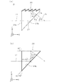
- FIG. 13 is a diagram for explaining the adjustment of the incident angle by the first optical element unit 21.
- FIG. 13A is a schematic diagram illustrating the variation in the emission angle of the laser light from the first optical element unit 21 according to the variation in the wavelength ⁇ of the laser light.
- the emission path from the reflective diffraction grating part 212 of the laser light emitted from the first light source part P1 at a predetermined reference temperature is indicated by a one-dot chain line L1a.
- FIG. 13B is a diagram exemplifying setting values for the reflection mode of the laser light inside the first optical element unit 21.
- the angle formed by the light beam L1 emitted from the first light source part P1 having a predetermined reference temperature and the perpendicular of the internal reflection surface 211b is 42.775 °, and the internal reflection surface
- the angle (diffraction angle) ⁇ 31 formed by the light beam incident on the upper surface of the first optical element portion 21 from 211b and the light beam emitted from the upper surface of the first optical element portion 21 is set to 41.03 °. .
- the angle (incident angle) ⁇ 32 formed by the laser beam 2 and the XY plane has the relationship of the following expression (5).
- the variation of the incident angle ⁇ due to the temperature variation (that is, the variation of the wavelength ⁇ ) of the first light source unit P1 represented by the equation (5) is the temperature variation (that is, the wavelength ⁇ ) of the first light source unit P1 represented by the above equation (3).
- Variation of the appropriate incident angle due to fluctuations in For this reason, the shape (for example, the length W a and the height H a of the bottom of the cross section, that is, the aspect ratio) of the reflection type diffraction grating unit 212 is appropriately adjusted, which is caused by the temperature variation of the first light source unit P1.
- the change in the appropriate incident angle due to the change in the wavelength ⁇ of the laser light can be canceled (ie, canceled) by the diffraction phenomenon by the first optical element unit 21.
- an appropriate laser for the diffraction grating portion 68 is changed in accordance with the change in the wavelength ⁇ of the laser light emitted from the first to fifth light source portions P1 to P5.
- the range of the incident angle of light changes, the incident angle with respect to the diffraction grating portion 68 is adjusted by the first to fifth optical element portions 21 to 25 provided on the optical path of the laser light. For this reason, the utilization efficiency of light can be raised and power consumption can also be reduced.
- the information recording apparatus 100 in order to reduce the thickness of the apparatus, laser light is irradiated from the side to the first to fifth slider parts 31 to 35, and the suspension parts 41b, 42b, 42c, 43b, 43c. And the recording disks 2a, 2b, 2c are generally set very narrowly to 0.5 mm or less.
- the appropriate incident angle with respect to the diffraction grating portion 68 is generally an oblique direction. For this reason, it is preferable to have a thin optical system that deflects the incident light to the diffraction grating portion 68 in an oblique direction and compensates for variations in the appropriate incident angle.
- the first to fifth optical element units 21 to 25 according to the present embodiment are provided as elements that are thin and compensate for fluctuations in the appropriate incident angle by utilizing reflection in the elements. ing.
- each suspension portion 41b, 42b, 42c, 43b, 43c On the other hand, the adhesive force when the first to fifth optical element portions 21 to 25 are bonded is improved. For this reason, the stability by fixing the first to fifth optical element portions 21 to 25 is increased.
- the first to fifth optical element portions 21 to 25 are configured by the reflective diffraction grating prism having the reflective diffraction grating portion 212, but the present invention is not limited to this.
- the first to fifth optical element portions 21 to 25 may be configured by prisms (transmission diffraction grating prisms) whose laser light exit surfaces are transmission diffraction gratings (transmission diffraction gratings). That is, an optical element having a wavelength dispersion characteristic that cancels the wavelength dispersion characteristic in the diffraction grating portion 68 may be employed.
- specific examples of the first to fifth optical element units 21A to 25A that constitute the arm mechanism 10A of the information recording apparatus 100A and to which the transmission diffraction grating prism is applied will be described.
- FIG. 14 is a schematic diagram illustrating a configuration example of the first optical element unit 21A according to the modification. Specifically, FIG. 14 shows a schematic cross-sectional view of the first optical element portion 21A cut along the XZ plane. Note that since the actual shape of the transmissive diffraction grating portion 215 is fine, in FIG. 14, the transmissive diffraction grating portion 215 is shown for convenience in order to clarify the shape of the transmissive diffraction grating portion 215. The unevenness is highlighted.
- the first optical element portion 21A has a substantially trapezoidal shape with a substantially constant XZ cross section and a substantially quadrangular prism shape extending along the Y axis, and a bottom surface (a surface on the ⁇ Z side) in the + X direction.
- the prism unit 213 includes a -X side incident surface 213a on which laser light emitted from the first light source unit P1 is incident, an upper surface 213U substantially parallel to the XY plane, and + X
- the laser beam traveling in the direction is reflected by a coated reflective film (for example, formed of Al, Ag, etc.) and deflected by about 60 ° to make the traveling direction of the laser beam obliquely downward (lower left in FIG. 14).
- a coated reflective film for example, formed of Al, Ag, etc.
- the transmissive diffraction grating portion 215 has a so-called blazed shape, and a plane (slope) linearly descending in the ⁇ Z direction and a plane substantially parallel to the YZ plane (vertical) as the XZ cross-sectional shape proceeds in the + X direction.
- a lower surface (exit surface) 215G that emits light by transmitting laser light.
- the exit surface 215G causes a laser light diffraction phenomenon.
- the incident angle ⁇ of the waveguide 60 to the diffraction grating portion 68 the relationship between the wavelength ⁇ 1 and the wavelength ⁇ 2 of the laser light as the temperature of the first light source portion P1 varies as shown in the above equation (2). 14, the angle (incident angle) ⁇ 41 formed by the laser beam having the wavelength ⁇ 1 and the XY plane and the angle (incident angle) ⁇ 42 formed by the laser beam having the wavelength ⁇ 2 and the XY plane, as shown in FIG. Have the relationship of the following formula (6).
- the variation of the incident angle ⁇ due to the temperature variation (that is, the variation of the wavelength ⁇ ) of the first light source unit P1 represented by the equation (6) is the temperature variation of the first light source unit P1 represented by the above equation (3) (that is, the wavelength ⁇ Variation of the appropriate incident angle due to fluctuations in Therefore, by appropriately adjusting the blazed shape of the transmissive diffraction grating unit 215, the variation of the appropriate incident angle due to the variation of the wavelength ⁇ of the laser light caused by the temperature variation of the first light source unit P1 can be reduced. It can be canceled (ie, canceled out) by the diffraction phenomenon by 21A.
- the reflective diffraction grating prism is preferable to the transmission diffraction grating prism.
- the position where the laser light is irradiated onto the diffraction grating part 68 is the wavelength of the laser light. Difficult to shift due to fluctuation of ⁇ .
- the preferred position setting is easier for the first optical element portion 21A employing the transmission type diffraction grating portion 215. Furthermore, as for the coating of the material for forming the reflective film (reflective material), the first optical element portion 21A formed by coating the reflective material on a flat surface is preferable in terms of easy manufacture.
- the laser beam is reflected by the reflective film, but without using the reflective film, the refractive index of the material forming the prism is adjusted as appropriate, and total reflection is used. You may make it reflect a laser beam.
- the first to fifth optical element portions 21 to 25 including the reflective diffraction grating portion 212 are employed.
- the first to fifth optical element portions including the transmissive diffraction grating portion 215 are provided.
- it is conceivable to employ various optical elements having wavelength dispersion characteristics such as a prism using a material having a very high refractive index compared to the refractive index in air without providing a diffraction grating portion.
- the information recording apparatuses 100 and 100A are configured as an optically assisted magnetic recording apparatus that records and reads information magnetically while applying heat to the recording medium with light.
- the present invention is generally applied to information recording apparatuses that record and read information using light irradiation, such as information recording apparatuses that record and read information by irradiating light onto a recording medium without using magnetism. May be.
- the present invention may be applied to general information recording apparatuses that can record information on a recording medium by irradiating the recording medium with light from an optical head.
- first to fifth optical element portions 21 to 25 reflect the laser beam twice inside, and the first optical element portions 21A to 25A according to the above specific examples internally reflect the laser beam 1 Although it was reflected once, it is not limited to this.
- the laser beam is deflected in the front surface of the diffraction grating part 68 using the diffraction phenomenon by using the diffraction phenomenon without reflecting the laser light even once, the laser light caused by the temperature fluctuation of the light source part.
- the traveling direction of the laser light is not deflected in the direction in which the fluctuation of the appropriate incident angle due to the fluctuation of the wavelength ⁇ is canceled (ie, canceled) by the diffraction phenomenon by the front diffraction grating. Accordingly, it is necessary to reflect the laser beam one or more times before entering the diffraction grating portion 68, and it is necessary to provide one or more reflecting surfaces on the first to fifth optical element portions 21 to 25 and 21A to 25A.
- the number of times (odd times or even times) the laser beam should be reflected is determined by the direction of the sawtooth inclined surface of the diffraction grating portion included in the first to fifth optical element portions 21 to 25 and 21A to 25A.
- the optical path can be adjusted by the first to fifth optical element portions 21 to 25 and 21A to 25A following the change in the range of the appropriate incident angle with respect to the grating portion 68.
- the first to fifth light source parts P1 to P5 are formed by the semiconductor laser chip.
- the present invention is not limited to this, and may be formed by various light emitting elements such as a light emitting diode (LED).
- LED light emitting diode
- the positions and the positions of the first to fifth light source portions P1 to P5 are considered. Varying the angle causes disadvantages such as unstable operation of the information recording apparatus 100 and increased power consumption in the movable part. Therefore, incidence by the first to fifth optical element parts 21 to 25 and 21A to 25A is caused. It is preferable to adjust the angle.
- the whole of the first optical element portion 21 except the reflective film 212M is made of resin, but is not limited thereto, and may be made of glass, for example.
- the prism portion 211 and the reflective diffraction grating portion 212 that constitute the first optical element portion 21 are formed using resin, but the present invention is not limited to this.
- the reflective diffraction grating portion 212 may be formed using resin for the prism portion 211 formed of glass.
Landscapes
- Physics & Mathematics (AREA)
- Electromagnetism (AREA)
- Engineering & Computer Science (AREA)
- Manufacturing & Machinery (AREA)
- Recording Or Reproducing By Magnetic Means (AREA)
- Optical Head (AREA)
- Magnetic Heads (AREA)
- Adjustment Of The Magnetic Head Position Track Following On Tapes (AREA)
- Supporting Of Heads In Record-Carrier Devices (AREA)
Abstract
Description
図1は、情報記録装置100の概略構成例を示す図である。図1および図1以降の図には、方位関係を明確化するためにXYZの直交する3軸が適宜付されている。
図4は、アーム機構10の構成例を示す模式図である。図4は、アーム機構10およびその周辺の構成を上方(+Z方向)から見た模式図であり、図4では、第1~5光源部P1~P5、第1~5光学素子部21~25、および第1~5スライダ部31~35の第1アーム部41に対する配置関係が破線で模式的に示されている。なお、図4では、各光源部P1~P5から射出されて、各光学素子部21~25を介して各スライダ部31~35に導入される光の各光路L1~L5が一点鎖線で示されている。また、図5は、光学素子部21の配置を例示する模式図であり、図5では、第1光源部P1から第1スライダ部31に至るレーザー光の光路L1が一点鎖線で示されている。
第1~5光源部P1~P5は、第1~5光学素子部21~25をそれぞれ介して第1~5スライダ部31~35に対して照射する光を発生させるものであり、例えば、一般的なCDプレイヤーやDVDレコーダーなどに使用される安価なファブリ・ペロー型のレーザーダイオードによって構成される。
図8は、回折格子部68が設けられた導波路60の素子(導波路グレーティング素子)の構成を例示する断面模式図である。
θ11<θ12 ・・・(3)。
第1~5光学素子部21~25は、それぞれ同様な構成を有するため、ここでは、第1光学素子部21を例にとって説明する。
本発明は上述の実施の形態に限定されるものではなく、本発明の要旨を逸脱しない範囲において種々の変更、改良等が可能である。
10,10A アーム機構
21~25,21A~25A 第1~5光学素子部
31~35,31A~35A 第1~5スライダ部
41~43 第1~3アーム部
51 光アシスト部
60 導波路
68 回折格子部
100,100A 情報記録装置
211,213 プリズム部
211a,213a 入射面
212 反射型回折格子部
212M 反射膜
213M 傾斜反射面
215 透過型回折格子部
211b,215G 射出面
P1~P5 第1~5光源部
Claims (8)
- アーム部と、
グレーティングカプラが設けられる導波路を含み且つ前記アーム部の一端側に取り付けられるヘッド部と、
前記グレーティングカプラに対して入射される光の光路上に配置されるとともに前記アーム部に取り付けられ且つ回折格子を有する光学素子と、
を備えることを特徴とするアーム機構。 - 請求項1に記載のアーム機構であって、
前記光学素子が、
プリズムを含むことを特徴とするアーム機構。 - 請求項1または請求項2に記載のアーム機構であって、
前記光学素子が、
少なくとも1つの反射面を有することを特徴とするアーム機構。 - 請求項3に記載のアーム機構であって、
前記回折格子が、
複数の反射面によって形成され且つ該複数の反射面による光の反射によって光の回折現象を生じさせる回折格子を含むことを特徴とするアーム機構。 - 請求項1から請求項4の何れかに記載のアーム機構と、
前記光学素子を介して前記ヘッド部に対して照射する光を発生させる光源部と、
前記ヘッド部に対して対向して配置される記録媒体と、
を備え、
前記ヘッド部が、
前記記録媒体に対して光を照射することで該記録媒体に対して情報の記録を行うことを特徴とする情報記録装置。 - 導波路に設けられたグレーティングカプラに対して入射される光の光路上に配置される光学素子であって、
光の波長変動に応じて、前記グレーティングカプラの適正入射角度の変動に対応するように光を射出する方向を変化させる回折格子を有することを特徴とする光学素子。 - 請求項6に記載の光学素子であって、
プリズムを含むことを特徴とする光学素子。 - 請求項6または請求項7に記載の光学素子であって、
少なくとも1つの反射面を有することを特徴とする光学素子。
Priority Applications (2)
| Application Number | Priority Date | Filing Date | Title |
|---|---|---|---|
| US12/992,496 US20110075526A1 (en) | 2008-05-14 | 2009-04-15 | Optical Element, Arm Mechanism, and Information Recording Device |
| JP2010511931A JPWO2009139258A1 (ja) | 2008-05-14 | 2009-04-15 | 光学素子、および光アシスト式の磁気記録ヘッド |
Applications Claiming Priority (2)
| Application Number | Priority Date | Filing Date | Title |
|---|---|---|---|
| JP2008126877 | 2008-05-14 | ||
| JP2008-126877 | 2008-05-14 |
Publications (1)
| Publication Number | Publication Date |
|---|---|
| WO2009139258A1 true WO2009139258A1 (ja) | 2009-11-19 |
Family
ID=41318631
Family Applications (1)
| Application Number | Title | Priority Date | Filing Date |
|---|---|---|---|
| PCT/JP2009/057576 WO2009139258A1 (ja) | 2008-05-14 | 2009-04-15 | 光学素子、アーム機構、および情報記録装置 |
Country Status (3)
| Country | Link |
|---|---|
| US (1) | US20110075526A1 (ja) |
| JP (1) | JPWO2009139258A1 (ja) |
| WO (1) | WO2009139258A1 (ja) |
Cited By (2)
| Publication number | Priority date | Publication date | Assignee | Title |
|---|---|---|---|---|
| WO2010104030A1 (ja) * | 2009-03-11 | 2010-09-16 | コニカミノルタオプト株式会社 | 光記録ヘッド及び光記録装置 |
| US11835840B2 (en) | 2016-09-29 | 2023-12-05 | Panasonic Intellectual Property Management Co., Ltd. | Optical scanning device that includes waveguides |
Families Citing this family (4)
| Publication number | Priority date | Publication date | Assignee | Title |
|---|---|---|---|---|
| US20100208557A1 (en) * | 2007-10-29 | 2010-08-19 | Manami Kuiseko | Optical Head and Optical Recording Device |
| WO2010016360A1 (ja) * | 2008-08-08 | 2010-02-11 | コニカミノルタオプト株式会社 | 光学装置、光記録ヘッド及び光記録装置 |
| JP5972100B2 (ja) * | 2012-08-13 | 2016-08-17 | キヤノン株式会社 | 反射型回折素子 |
| US9165591B2 (en) * | 2013-08-07 | 2015-10-20 | Seagate Technology Llc | Grating based laser and power monitor for a heat-assisted magnetic recording device |
Citations (3)
| Publication number | Priority date | Publication date | Assignee | Title |
|---|---|---|---|---|
| JPH0210527A (ja) * | 1988-06-29 | 1990-01-16 | Hitachi Ltd | 光集積回路 |
| JPH02162304A (ja) * | 1988-12-16 | 1990-06-21 | Fuji Photo Film Co Ltd | 導波光と外部光との結合方法 |
| JP2007095167A (ja) * | 2005-09-28 | 2007-04-12 | Konica Minolta Holdings Inc | 熱アシスト磁気記録ヘッド及び磁気記録装置 |
Family Cites Families (6)
| Publication number | Priority date | Publication date | Assignee | Title |
|---|---|---|---|---|
| US5541906A (en) * | 1994-07-29 | 1996-07-30 | Olympus Optical Co., Ltd. | Optical head for magneto-optical record medium |
| JP3660415B2 (ja) * | 1995-02-07 | 2005-06-15 | 富士通株式会社 | 光学記憶装置用光学デバイス |
| JP3062099B2 (ja) * | 1996-02-06 | 2000-07-10 | 日本電気株式会社 | 光ヘッド装置 |
| JP3439903B2 (ja) * | 1996-03-11 | 2003-08-25 | 富士通株式会社 | 光ディスク装置用光学ヘッド |
| AU2003218274A1 (en) * | 2002-06-28 | 2004-01-19 | Seagate Technology Llc | Heat assisted magnetic recording head with a planar waveguide |
| US7349612B2 (en) * | 2003-01-28 | 2008-03-25 | Nippon Sheet Glass Company, Limited | Optical element, optical circuit provided with the optical element, and method for producing the optical element |
-
2009
- 2009-04-15 JP JP2010511931A patent/JPWO2009139258A1/ja active Pending
- 2009-04-15 US US12/992,496 patent/US20110075526A1/en not_active Abandoned
- 2009-04-15 WO PCT/JP2009/057576 patent/WO2009139258A1/ja active Application Filing
Patent Citations (3)
| Publication number | Priority date | Publication date | Assignee | Title |
|---|---|---|---|---|
| JPH0210527A (ja) * | 1988-06-29 | 1990-01-16 | Hitachi Ltd | 光集積回路 |
| JPH02162304A (ja) * | 1988-12-16 | 1990-06-21 | Fuji Photo Film Co Ltd | 導波光と外部光との結合方法 |
| JP2007095167A (ja) * | 2005-09-28 | 2007-04-12 | Konica Minolta Holdings Inc | 熱アシスト磁気記録ヘッド及び磁気記録装置 |
Cited By (2)
| Publication number | Priority date | Publication date | Assignee | Title |
|---|---|---|---|---|
| WO2010104030A1 (ja) * | 2009-03-11 | 2010-09-16 | コニカミノルタオプト株式会社 | 光記録ヘッド及び光記録装置 |
| US11835840B2 (en) | 2016-09-29 | 2023-12-05 | Panasonic Intellectual Property Management Co., Ltd. | Optical scanning device that includes waveguides |
Also Published As
| Publication number | Publication date |
|---|---|
| JPWO2009139258A1 (ja) | 2011-09-15 |
| US20110075526A1 (en) | 2011-03-31 |
Similar Documents
| Publication | Publication Date | Title |
|---|---|---|
| US8730780B2 (en) | Light delivery waveguide | |
| JP5777585B2 (ja) | 導波路を備えた装置、方法、およびシステム | |
| US7898759B2 (en) | Thermally assisted magnetic recording head and magnetic recording apparatus | |
| KR100738078B1 (ko) | 근접장광발생장치와 이를 채용한 열보조 자기기록헤드 | |
| US20080002529A1 (en) | Optical head and optical recording apparatus | |
| WO2009139258A1 (ja) | 光学素子、アーム機構、および情報記録装置 | |
| WO2010010806A1 (ja) | 光記録ヘッド及び光記録装置 | |
| KR20090037803A (ko) | 헤드 슬라이더 | |
| JP4685625B2 (ja) | 回折格子 | |
| US8072847B2 (en) | Optical device, optically heat assisted magnetic recording head and optically heat assisted magnetic recording apparatus, having intensity point deviated from axis of the core | |
| US8274866B2 (en) | Optical recording head and optical recording apparatus | |
| JP4479860B2 (ja) | 光記録ヘッド及び光記録装置 | |
| JP2009104734A (ja) | 微小スポット生成構造及び光ヘッド | |
| JP4400697B2 (ja) | 情報記録装置、およびアーム機構 | |
| JP2013004160A (ja) | 光アシスト磁気ヘッド及び光学的結合構造 | |
| JP2009283096A (ja) | 光記録ヘッド、光アシスト磁気記録ヘッド、及び光アシスト磁気記録装置 | |
| US8588036B1 (en) | Optical device including interlayer | |
| JP2009283051A (ja) | 光学素子、光記録ヘッド及び光記録装置 | |
| WO2010082404A1 (ja) | 光学装置、光記録ヘッド及び光記録装置 | |
| WO2010010796A1 (ja) | ヘッド機構、光アシスト式磁気記録装置、および光記録装置 | |
| JP2009301602A (ja) | 光学素子、光記録ヘッド及び光記録装置 | |
| WO2011078025A1 (ja) | 光アシスト磁気ヘッド | |
| JP2008305501A (ja) | 光学素子、光ヘッド | |
| JP2010267354A (ja) | 光学素子、光アシスト磁気記録ヘッド、及び光アシスト磁気記録装置 |
Legal Events
| Date | Code | Title | Description |
|---|---|---|---|
| 121 | Ep: the epo has been informed by wipo that ep was designated in this application |
Ref document number: 09746465 Country of ref document: EP Kind code of ref document: A1 |
|
| WWE | Wipo information: entry into national phase |
Ref document number: 12992496 Country of ref document: US Ref document number: 2010511931 Country of ref document: JP |
|
| NENP | Non-entry into the national phase |
Ref country code: DE |
|
| 122 | Ep: pct application non-entry in european phase |
Ref document number: 09746465 Country of ref document: EP Kind code of ref document: A1 |