WO2009131048A1 - プラズマ処理装置およびそれを用いたプラズマ処理方法 - Google Patents
プラズマ処理装置およびそれを用いたプラズマ処理方法 Download PDFInfo
- Publication number
- WO2009131048A1 WO2009131048A1 PCT/JP2009/057610 JP2009057610W WO2009131048A1 WO 2009131048 A1 WO2009131048 A1 WO 2009131048A1 JP 2009057610 W JP2009057610 W JP 2009057610W WO 2009131048 A1 WO2009131048 A1 WO 2009131048A1
- Authority
- WO
- WIPO (PCT)
- Prior art keywords
- electrode
- plasma processing
- piece
- support
- distance
- Prior art date
Links
Images


Classifications
-
- C—CHEMISTRY; METALLURGY
- C23—COATING METALLIC MATERIAL; COATING MATERIAL WITH METALLIC MATERIAL; CHEMICAL SURFACE TREATMENT; DIFFUSION TREATMENT OF METALLIC MATERIAL; COATING BY VACUUM EVAPORATION, BY SPUTTERING, BY ION IMPLANTATION OR BY CHEMICAL VAPOUR DEPOSITION, IN GENERAL; INHIBITING CORROSION OF METALLIC MATERIAL OR INCRUSTATION IN GENERAL
- C23C—COATING METALLIC MATERIAL; COATING MATERIAL WITH METALLIC MATERIAL; SURFACE TREATMENT OF METALLIC MATERIAL BY DIFFUSION INTO THE SURFACE, BY CHEMICAL CONVERSION OR SUBSTITUTION; COATING BY VACUUM EVAPORATION, BY SPUTTERING, BY ION IMPLANTATION OR BY CHEMICAL VAPOUR DEPOSITION, IN GENERAL
- C23C16/00—Chemical coating by decomposition of gaseous compounds, without leaving reaction products of surface material in the coating, i.e. chemical vapour deposition [CVD] processes
- C23C16/44—Chemical coating by decomposition of gaseous compounds, without leaving reaction products of surface material in the coating, i.e. chemical vapour deposition [CVD] processes characterised by the method of coating
- C23C16/50—Chemical coating by decomposition of gaseous compounds, without leaving reaction products of surface material in the coating, i.e. chemical vapour deposition [CVD] processes characterised by the method of coating using electric discharges
- C23C16/505—Chemical coating by decomposition of gaseous compounds, without leaving reaction products of surface material in the coating, i.e. chemical vapour deposition [CVD] processes characterised by the method of coating using electric discharges using radio frequency discharges
- C23C16/509—Chemical coating by decomposition of gaseous compounds, without leaving reaction products of surface material in the coating, i.e. chemical vapour deposition [CVD] processes characterised by the method of coating using electric discharges using radio frequency discharges using internal electrodes
- C23C16/5096—Flat-bed apparatus
-
- H—ELECTRICITY
- H01—ELECTRIC ELEMENTS
- H01J—ELECTRIC DISCHARGE TUBES OR DISCHARGE LAMPS
- H01J37/00—Discharge tubes with provision for introducing objects or material to be exposed to the discharge, e.g. for the purpose of examination or processing thereof
- H01J37/32—Gas-filled discharge tubes
- H01J37/32009—Arrangements for generation of plasma specially adapted for examination or treatment of objects, e.g. plasma sources
- H01J37/32082—Radio frequency generated discharge
- H01J37/32091—Radio frequency generated discharge the radio frequency energy being capacitively coupled to the plasma
-
- H—ELECTRICITY
- H01—ELECTRIC ELEMENTS
- H01J—ELECTRIC DISCHARGE TUBES OR DISCHARGE LAMPS
- H01J37/00—Discharge tubes with provision for introducing objects or material to be exposed to the discharge, e.g. for the purpose of examination or processing thereof
- H01J37/32—Gas-filled discharge tubes
- H01J37/32431—Constructional details of the reactor
- H01J37/32532—Electrodes
- H01J37/32568—Relative arrangement or disposition of electrodes; moving means
Definitions
- the present invention relates to a plasma processing apparatus and a plasma processing method using the same, and more particularly to an apparatus structure and a processing method capable of adjusting a distance between electrodes.
- a parallel plate type plasma processing apparatus is a device in which a substrate, which is an object to be processed, is placed on one of a cathode electrode and an anode electrode, and plasma processing is performed on the substrate surface by causing plasma discharge between the electrodes in a reactive gas atmosphere. is there.
- the cathode electrode and the anode electrode are fixed to each other. The distance (for example, about 5 to 30 mm) is kept constant.
- This slide type plasma processing apparatus has a lower electrode and two linear guides mounted on a main base, a slide member placed on each linear guide so as to straddle the lower electrode, and a lower electrode.
- an upper electrode attached to the slide member with a bolt and a ball screw mechanism for horizontally moving the slide member and the upper electrode relative to the lower electrode are provided.
- the upper electrode is attached to the slide member via an adjustment mechanism having a gap adjusting screw or a spacer so that the distance between the electrodes can be adjusted according to the type and thickness of the substrate. Yes.
- This elevating plasma apparatus includes two linear guides that support the upper electrode so as to be movable up and down, a movable piece connected to one end surface of the upper electrode, and a ball screw mechanism that moves the upper electrode up and down via the movable piece. It has.
- the slide type plasma processing apparatus since the size of the main base for laying the rail is larger than the size of the lower electrode, the slide type plasma processing apparatus has a new problem that the installation area of the apparatus is greatly increased.
- the upper electrode and the slide member are connected at four locations by bolts and an adjustment mechanism, it is difficult to manually and quickly adjust the distance between the four electrodes at the same location.
- the distance between the electrodes since the distance between the electrodes depends on the movement accuracy of the ball screw mechanism, a highly accurate ball screw mechanism is required when the distance between the electrodes is small.
- the discharge area of the electrode becomes large, there is a problem that the configuration of the apparatus becomes complicated because it is necessary to provide ball screw mechanisms at a plurality of locations and control each of them.
- the present invention has been made in view of the above-described problems, and an object of the present invention is to provide a plasma processing apparatus and a plasma processing method using the same that can adjust the inter-electrode distance with high accuracy while having a simple structure.
- the reaction chamber, the gas introduction portion for introducing the reaction gas into the reaction chamber, the exhaust portion for exhausting the reaction gas from the reaction chamber, and the plasma discharge in the reaction gas disposed in the reaction chamber are provided.
- a parallel plate-shaped first electrode and second electrode a moving mechanism that supports or fixes the first electrode or the second electrode and is movable in the opposing direction, and supports or supports at least one of the first electrode and the second electrode
- the first electrode or the second electrode is moved by the moving mechanism, and the peripheral edges of the first electrode and the second electrode are in contact with the fixed piece, whereby the first electrode and the second electrode
- a plasma processing apparatus capable of determining a minimum inter-electrode distance from an electrode is provided.
- a method for plasma processing a surface of a substrate placed on the first electrode or the second electrode using the plasma processing apparatus depending on the purpose of the plasma processing. After the adjustment of the distance between the first electrode and the second electrode to the minimum inter-electrode distance by the operation of the moving mechanism, the plasma treatment between the narrow electrodes is caused to perform plasma discharge in the reaction gas between the first electrode and the second electrode.
- the plasma is discharged between the first electrode and the second electrode in the reactive gas between the wide electrodes.
- the plasma processing apparatus of the present invention includes a moving mechanism that supports or fixes the first electrode or the second electrode and is movable in the opposite direction, and a fixed piece that supports or fixes at least one of the first electrode and the second electrode. Since the first electrode or the second electrode is moved by the moving mechanism, and the peripheral portions of the first electrode and the second electrode are in contact with the fixed piece, the first electrode and the second electrode The minimum interelectrode distance is easily determined. Furthermore, since the first electrode and the second electrode can be moved in a relatively separated direction by the moving mechanism, the distance between the first electrode and the second electrode can be increased to an arbitrary interelectrode distance.
- the narrow electrode plasma processing in which the distance between the first electrode and the second electrode is set to the minimum electrode distance, and the electrode distance between the first electrode and the second electrode which is wider than the minimum electrode distance are set. It is possible to perform either one of the wide electrode plasma treatments or both treatments successively in any order (plasma treatment method). Furthermore, by widening the distance between the electrodes, it is possible to easily install the substrate as the object to be processed between the electrodes and take out the substrate from between the electrodes.
- Embodiment 1 of the plasma processing apparatus of this invention It is an internal block diagram seen from one side of Embodiment 1 of the present invention. It is an internal block diagram in the state without the electrode in FIG. It is an internal block diagram seen from the upper part of Embodiment 1 of this invention. It is a figure explaining the positional relationship of the fixed piece and support piece in Embodiment 1 of this invention. It is explanatory drawing which shows the state which the 1st electrode in Embodiment 1 of this invention raises / lowers. It is composition explanatory drawing which shows the fixed piece in Embodiment 1 of this invention. It is composition explanatory drawing which shows the support piece in Embodiment 1 of this invention.
- the plasma processing apparatus of the present invention includes a reaction chamber, a gas introduction unit for introducing a reaction gas into the reaction chamber, an exhaust unit for exhausting the reaction gas from the reaction chamber, and a plasma discharge disposed in the reaction chamber.
- the plasma processing apparatus includes a plasma processing (narrow electrode plasma processing step) in a state where the distance between the first electrode and the second electrode is set to the minimum inter-electrode distance, and an inter-electrode distance wider than the minimum inter-electrode distance.
- One or both of the plasma processing (wide electrode plasma processing step) with the distance set can be arbitrarily performed.
- by relatively moving the first and second electrodes to widen the space between the electrodes it becomes easy to carry the substrate between the electrodes, carry the substrate from between the electrodes, and clean the electrode discharge surface.
- This plasma processing apparatus includes an upper and lower parallel type in which one set or a plurality of sets of parallel plate type discharge parts (electrode bodies) including a first electrode and a second electrode are arranged in the vertical direction, and one of parallel plate type discharge parts.
- the present invention can be applied to both a left-right parallel type in which a set or a plurality of sets are arranged in the left-right direction.
- the first and second electrodes are arranged horizontally
- the first and second electrodes are arranged vertically.
- the plasma processing apparatus can be applied to both film formation and etching.
- the mounting method is not particularly limited as long as the fixing piece is provided in the reaction chamber so as to contact the peripheral portions of the first electrode and the second electrode to determine the minimum interelectrode distance. Absent.
- a support part that supports at least one of the first electrode and the second electrode is provided in the reaction chamber, and a fixed piece is attached to the support part, or a fixed piece is attached to the inner wall surface of the chamber constituting the reaction chamber or the frame of the chamber be able to.
- a flexible connection member when the electrode to be moved is connected to a connection member such as a power supply cable, a grounding member, or a gas introduction pipe.
- the connecting member it is necessary for the connecting member to allow and follow the movement of the electrode. If the space between the inner wall surface of the chamber and the peripheral edge portion of the electrode has a clearance, the connecting member allows the movement of the electrode and can easily follow it. In this case, it is preferable to provide a support portion in the reaction chamber and attach a fixed piece to the support portion.
- a support portion at least a support member such as a column member, a beam member, or a frame member for attaching the fixed piece is provided in the reaction chamber. What is necessary is just to be provided.
- the structure of the moving mechanism is not particularly limited as long as the first electrode or the second electrode is supported or fixed and can move in the opposite direction, and either the first electrode or the second electrode is moved. Also good.
- the moving mechanism is configured to move the electrode in the vertical direction when the plasma processing apparatus is a vertical parallel type, and is configured to move the electrode in the horizontal direction when the plasma processing apparatus is a horizontal parallel type.
- Examples of the moving mechanism for moving the electrode in the vertical direction or the horizontal direction include a hydraulic cylinder mechanism, a ball screw mechanism, a link mechanism using these as a power source, etc.
- a hydraulic cylinder mechanism is preferred.
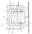
- FIG. 1 is a configuration diagram viewed from the front showing Embodiment 1 of the plasma processing apparatus of the present invention
- FIG. 2 is an internal configuration diagram viewed from one side of Embodiment 1 of the present invention
- FIG. 4 is an internal configuration diagram viewed from above the first embodiment of the present invention
- FIG. 5 is a diagram of positions of the fixed piece and the support piece in the first embodiment of the present invention.
- FIG. 6 is an explanatory diagram illustrating a state in which the first electrode according to Embodiment 1 of the present invention is raised and lowered.
- This plasma processing apparatus is a vertically parallel type, and exhausts the reaction gas G1 from the reaction chamber R, a chamber C1 constituting the reaction chamber R, a gas introduction part 1a for introducing the reaction gas G1 indicated by an arrow into the reaction chamber R, and the like.
- the first electrode 1 is a cathode electrode
- the second electrode is an anode electrode
- a substrate S1 (see FIG. 6) that is an object to be processed is placed on the second electrode 2, and the surface of the substrate S1
- a plasma processing apparatus for forming a predetermined film is illustrated.
- the number of the discharge parts 3 is not limited to two, One or three There may be more than one.
- the chamber C1 includes a metal box-shaped main body C1a and metal legs C1b that support the main body C1a on the floor surface of the installation place.
- the second electrode 2 is grounded via two conductive grounding members 8 and a metal chamber C1.
- the exhaust unit 6 includes a vacuum pump 6a, an exhaust pipe 6b connecting the vacuum pump 6a and the reaction chamber R, and a pressure controller 6c disposed between the reaction chamber R and the vacuum pump 6a in the exhaust pipe 6b. .
- the power supply unit E generates, for example, 10 W to 100 kW of power at a frequency of AC 1.00 MHz to 60 MHz, specifically, 10 W to 10 kW of power at 13.56 MHz to 60 MHz, and supplies the plasma to each first electrode 1. Excitation power source.
- the power supply unit E includes a high-frequency generator e1, an impedance matching unit e2 for supplying equal power to each first electrode 1, and a power supply cable e3 that connects these to the power supply location of each first electrode 1.
- An amplifier (not shown) may be further provided.
- the connection side portion of the power supply cable e3 connected to the first electrode 1 allows the first electrode 1 to move up and down. Flexible so that it can follow.
- the power supply cable between the box-shaped main body C1a of the chamber C1 and the first electrode 1 can be a flexible metal net member.
- the feeding position of the first electrode 1 is the center position in the front-rear direction of the right end surface of the first electrode 1.
- the grounding location of the second electrode 2 is positioned on both sides of the center in the front-rear direction of the left end surface of the second electrode 2.
- Each first electrode (cathode electrode) 1 is rectangular and is made of stainless steel, aluminum alloy, or the like.
- the dimension of each first electrode 1 is set to an appropriate value according to the dimension of the substrate S1 to be deposited, and is designed with a plane size slightly larger than the second electrode 2 and the same thickness as the second electrode 2. be able to.
- Each first electrode 1 has a hollow inside, and a large number of through holes are formed in the plasma discharge surface facing the paired second electrode 2 by drilling. This drilling can be performed, for example, with circular holes having a diameter of 0.1 mm to 2 mm at a pitch of several mm to several cm.
- a gas introduction pipe as a gas introduction part 1 a is connected to one end face of each first electrode 1.
- a gas supply source (not shown) and the gas introduction part 1a are connected by a connection pipe, the reaction gas G1 is supplied from the gas supply source to the inside of the first electrode 2, and is directed from the many through holes toward the surface of the substrate S1. Erupt. Moreover, since the 1st electrode 1 raises / lowers as mentioned above, at least the connection side part of the gas introduction pipe
- the gas introduction pipe in the portion between the box-type main body C1a of the chamber C1 and the first electrode 1 can be a flexible fluororesin pipe.
- the source gas for example, SiH 4 (monosilane) gas diluted with H 2 is used.
- Each second electrode 2 is rectangular, has a heater (not shown) inside, and has a substrate S1 installed on the upper surface, and heats the substrate S1 during film formation under plasma discharge.
- the substrate S1 is generally a silicon substrate or a glass substrate, but is not particularly limited thereto.
- Each second electrode 2 is made of a material having conductivity and heat resistance, such as stainless steel, aluminum alloy, and carbon.
- the dimension of each second electrode 2 is determined to an appropriate value in accordance with the dimension of the substrate S1 for forming a thin film. For example, the size of the second electrode 2 is 1000 to 1500 mm ⁇ 600 to 1000 mm, while the size of the substrate S1 is 900 to 1200 mm ⁇ 400 to 900 mm.
- the length in the left-right direction of the second electrode 2 is set shorter than the length in the left-right direction of the first electrode 1 so as not to collide with the second electrode 2 when the support piece 5c described in detail later is lowered. (See FIGS. 1 and 6).
- the heater built in each second electrode 2 controls the heating of the second electrode 2 to about room temperature to about 300 ° C., for example, a sealed heating device such as a sheath heater and a thermocouple in a cylinder made of aluminum alloy. It is possible to use a built-in sealed temperature sensor such as.
- the support unit 4 includes a plurality of support columns 4a disposed around the first electrode 1 and the second electrode 2 in the reaction chamber R, a frame body 4b that connects the plurality of support columns 4a,
- This is a support structure in which a first electrode fixing piece 7a and a second electrode fixing piece 7b attached to the support column 4a are integrated.
- the first electrode fixing piece 7a and the second electrode fixing piece 7b may be referred to as the first fixing piece 7a and the second fixing piece 7b, or may be collectively referred to as the fixing pieces 7a and 7b.
- four support columns 4a are fixed to the inner surface of the bottom wall of the chamber C1 so as to be arranged near the four corners of the electrodes 1 and 2.
- the upper ends of the four supporting columns 4a are connected by a rectangular frame 4b. Moreover, the 1st fixing piece 7a and the 2nd fixing piece 7b are each attached inward at two places of the predetermined height position of each support
- the frame 4b is formed by combining four straight members.
- first fixing pieces 7a that horizontally support the first electrodes 1 of the upper and lower discharge parts 3 and eight second fixings that horizontally support the second electrodes 2 of the upper and lower discharge parts 3.
- the piece 7b is attached to a predetermined height position of the four supporting columns 4a.
- the first and second fixed pieces 7a and 7b in each stage are the minimum inter-electrode distance between the first electrode 1 and the second electrode 2 in each discharge section 3.
- A is arranged at a height position where A is a predetermined distance
- the upper second fixing piece 7b and the lower first fixing piece 7a have a predetermined distance B between the discharge parts between the upper and lower discharge parts 3. It is arranged at the height position.
- the lower second fixed piece 7b that supports the second electrode 2 is higher than the upper first fixed piece 7a so that the second electrode 2 that is shorter in the left-right direction than the first electrode 1 can be supported. It is formed long inward.
- the distance A between the electrodes is set to 2 to 30 mm, and the distance B between the discharge parts is set to 4 to 60 mm or more.
- the accuracy of the inter-electrode distance A in the plane is preferably within a few percent, and particularly preferably 1% or less.
- the material of the supporting column 4a may be either conductive or insulating, but from the viewpoint of workability and heat resistance, for example, a metal material such as stainless steel or aluminum alloy is preferable.
- Each fixed piece 7a, 7b is made of, for example, a metal oxide such as alumina or zirconia so that heat from the first electrode 1 and the second electrode 2 is not easily transmitted to the support column 4a via each fixed piece 7a, 7b.
- insulating materials such as a ceramic, and it is especially comprised so that zirconia with low heat conductivity may interpose between the 1st electrode 1 and 2nd electrode, and the support
- all of the fixed pieces 7a and 7b may be made of an insulating material, but a part thereof may be made of an insulating material.
- the insulating material is interposed in this way, the heat of the first electrode 1 and the second electrode supported by the fixed pieces 7a and 7b is not easily transmitted to the support column 4a, and the heat of the support column 4a Elongation due to expansion can be suppressed.
- the fixing pieces 7a and 7b When fixing pieces 7a and 7b having an insulating member made of an insulating material are attached to a supporting column 4a made of a metal material, the fixing pieces 7a and 7b are illustrated in FIG. 7A or FIG. 7B, for example. It may be configured as described.
- the fixed piece 7a includes, for example, a metal receiving piece 7a 1 welded to a predetermined height position of the support column 4a, and an insulating member 7a 2 installed on the receiving piece 7a 1.
- the fixed piece 7a is made of a metal material having impact resistance (for example, iron-chromium metal) on the insulating member 7a 2 in contact with the first electrode 1 shown in FIG. 7 (A).
- the formed metal piece 7a 3 can be placed, and the receiving piece 7a 1 , the insulating member 7a 2 and the metal piece 7a 3 can be connected by the bolt / nut connection.
- FIG. 7B only the fixed piece 7a is shown, but the fixed piece 7b is the same as the fixed piece 7a.
- the moving mechanism 5 is a frame body that connects the four lifting columns 5a arranged around the first electrode 1 and the second electrode 2 in the reaction chamber R and the upper and lower portions of the four lifting columns 5a. 5b, a plurality of support pieces 5c attached to the lifting column 5a or the frame 5b so as not to interfere with the respective fixed pieces 7a, 7b, a lifting drive unit 5d, the lifting drive unit 5d, and the lifting column 5a or frame.
- a connecting portion 5e that connects the body 5b and transmits the lifting / lowering operation of the lifting / lowering drive portion 5d is provided.
- the moving mechanism 5 separates the first electrode 1 on the first fixed piece 7a from the second electrode 2 by the ascending operation of the predetermined stroke (see FIG.
- FIG. 6A shows a state where the minimum interelectrode distance A is determined by the first electrode 1 contacting the first fixed piece 7a and the second electrode 2 contacting the second fixed piece 7b. ing.
- the four lifting columns 5a are arranged in the vicinity of the four supporting columns 4a. More specifically, each lifting column 5a is between two supporting columns 4a, and the distance from each lifting column 5a to each electrode is substantially equal to the distance from each supporting column 4a to each electrode. Has been placed. And the upper part and the lower part of the four raising / lowering support
- the frame 5b is formed by combining four straight members.
- two support pieces 5c are attached inwardly to the four lifting columns 4a so that the first electrodes 1 of the upper and lower discharge portions 3 can be moved up and down.
- the projecting dimension to the inside of the support piece 5c is set to a length that does not collide with the second electrode 2 when the support piece 5c is lowered.
- the upper and lower support pieces 5c corresponding to each lifting column 5a are The discharge part 3 is located slightly below the lower surface of the second electrode 2 (for example, about 5 mm).
- the reason for lowering the support piece 5c below the lower surface of the second electrode 2 is that if there is a support piece that does not support the first electrode in the plasma discharge region of the discharge part 3, the support piece interferes with the plasma. This is because uniform plasma cannot be generated in the discharge space.
- the elevating drive unit 5d is a hydraulic cylinder mechanism including two hydraulic cylinders, and is fixed to the floor surface of the installation place so that each hydraulic cylinder expands and contracts in the vertical direction.
- the connecting portion 5e includes a connecting plate 5e1 fixed to the ends of the telescopic rods of the two hydraulic cylinders, and a connecting column 5e2 that connects the connecting plate 5e1 and the lower ends of the four lifting columns 5a.
- the lifting / lowering operation of 5d is synchronously transmitted to the four lifting columns 5a and the supporting pieces 5c attached thereto via the coupling plate 5e1 and the four coupling columns 5e2.
- the limit of the ascending operation of the elevating drive unit 5 is set such that the upper frame body 5 b does not hit the upper frame body 4 b of the support unit 4.
- the four connecting struts 5e2 of the connecting portion 5e are inserted through four insertion holes formed in the bottom wall of the chamber C1 so as to be vertically movable.
- a cylindrical guide member 5f is attached to the bottom wall of the chamber C1 so as to communicate with the four insertion holes and guide each connection column 5e2, and is connected between the insertion hole and the connection column 5e2 and to the guide member 5f.
- the gap between the columns 5e2 is sealed with a heat-resistant sealing material.
- the lifting column 5a and the connecting column 5e2 may be either conductive or insulating, but from the viewpoint of workability and heat resistance, for example, a metal material such as stainless steel or aluminum alloy is preferable.
- the support piece 5c is made of an insulating material such as a metal oxide such as alumina or zirconia or a ceramic so that current does not flow from the first electrode 1 to the lifting column 5a via the support piece 5c.
- zirconia having low thermal conductivity is configured to be interposed between the first electrode 1 and the lifting column 5a.
- the support piece 5c that is in contact with the first electrode 1 is formed of a metal material having impact resistance, and examples of such a metal material include iron-chromium metal.
- the supporting column 4a and the lifting column 5a receive thermal radiation from the plasma and thermally expand to slightly extend. Therefore, it is preferable that the thermal expansion coefficient of the supporting column 4a and the lifting column 5a is the same.
- the supporting column 4a and the lifting column 5a are preferably formed of the same material, More preferably, the various dimensions and shapes are made of the same member.
- the distance from the plasma discharge region between the first electrode 1 and the second electrode 2 to the support column 4a as described above. The distance from the plasma discharge region to the lifting column 5a is set to be the same.
- the extension amount of the support column 4a during plasma processing is equal to the extension amount of the lifting column 5a, so that the above-described wide area for supporting the first electrode 1 by the support piece 5c of the moving mechanism 5 is provided.
- the interelectrode plasma processing step it is possible to suppress a variation in a predetermined interelectrode distance.
- the narrow electrode plasma processing step of supporting the first and second electrodes 1 and 2 with the first and second fixing pieces 7 a and 7 b of the support portion 4 the minimum inter-electrode distance A due to the extension of the support column 4. The fluctuation of is even smaller.
- the support piece 5a When the support piece 5c having an insulating member made of an insulating material is attached to the lifting column 5a made of a metal material, the support piece 5a is configured as shown in FIG. 8A or FIG. 8B, for example. May be.
- the support piece 5a In the case of FIG. 8A, the support piece 5a is configured by connecting a metal receiving piece 5c 1 and an insulating member 5c 2 with bolts and nuts in the same manner as the fixing piece 7a described in FIG. 7A. .
- the support piece 5a is made of an impact-resistant metal material (for example, iron-chromium metal) on the insulating member 5c 2 in the same manner as the fixing piece 7a described in FIG. 7B.
- the formed metal piece 5c 3 is placed, and the receiving piece 5c 1 , the insulating member 5c 2 and the metal piece 5c 3 are connected by bolts and nuts.
- the lowermost support shown in FIG. 6B is supported by the ascending operation of the moving mechanism 5 caused by the elevating drive unit 5d extending.
- the piece 5c rises to receive the first electrode 1, and the support piece 5c further rises to separate the first electrode 1 from the second electrode 2 (see FIG. 6A).
- the support piece 5 c does not collide with the second electrode 2.
- the substrate S1 can be easily installed on the second electrode 2, or the substrate S1 can be easily taken out from the second electrode 2. Further, from the state of FIG.
- the lowermost support piece 5c is lowered by the lowering operation of the moving mechanism 5 due to the shortening operation of the elevating drive unit 5d, and the first electrode 1 is placed on the first fixed piece 7a.
- the minimum inter-electrode distance A is determined, and the support piece 5c is lowered below the lower surface of the second electrode 2 to enable the narrow inter-electrode plasma processing.
- the uppermost support piece 5c is lowered, and the lowering of the support piece 5c is stopped before the first electrode 1 is placed on the first fixed piece 7a.
- FIG. 6A the lowermost support piece 5c is lowered by the lowering operation of the moving mechanism 5 due to the shortening operation of the elevating drive unit 5d, and the first electrode 1 is placed on the first fixed piece 7a.
- the support piece 5c rises to receive the first electrode 1 and stops before the rise of the support piece 5c reaches the uppermost position, so that a wide electrode wider than the minimum interelectrode distance A is obtained.
- the distance between the electrodes (for example, about 15 to 30 mm) is determined, and the plasma treatment between the wide electrodes becomes possible.
- plasma discharge is performed in the first reaction gas between the first electrode 1 and the second electrode 2 after adjusting to the minimum interelectrode distance A according to the purpose of the plasma processing.
- the second reaction between the first electrode 1 and the second electrode 2 after adjusting to a wide interelectrode distance wider than the minimum interelectrode distance A (see FIG. 6A).
- “according to the purpose of the plasma treatment” means that it corresponds to the material of the film to be deposited, the density of the film, the thickness of the substrate S1, and the like.
- Examples of the narrow electrode plasma processing step include a plasma CVD step of forming a silicon-based semiconductor film containing crystals on the surface of the substrate S1, and the wide electrode plasma processing step includes amorphous silicon on the surface of the substrate S1.
- a plasma CVD process for forming a semiconductor film can be given.
- the plasma CVD process for forming a silicon-based semiconductor film containing such a crystal and the plasma CVD process for forming an amorphous silicon-based semiconductor film are performed in only one of the processes, or both processes in any order. Can be performed continuously.
- the reactive gas G1 that is a film material is filled in the gap between the first electrode 1 and the second electrode 2 at a predetermined flow rate and pressure, and high frequency power is applied to the first electrode 1 and the second electrode 2.
- a glow discharge region (plasma discharge region) is generated between the first electrode 1 and the second electrode 2, and an amorphous film, a crystalline film, or a laminated film of these is efficiently formed on the substrate S1 with high accuracy.
- a silicon thin film having a thickness of 300 nm can be deposited with a thickness distribution within ⁇ 10%.
- FIG. 9 is an explanatory view showing a state in which the second electrode moves up and down in Embodiment 2 of the plasma processing apparatus of the present invention.
- the plasma processing apparatus according to the second embodiment is a vertically parallel type plasma processing apparatus for film formation, in which the first electrode fixing piece and the second electrode fixing piece described in the first embodiment are integrally formed.
- the first electrode 1 is placed on the fixed piece 7, and the second electrode 2 is pressed against the lower surface of the fixed piece 7 by the ascending operation of the moving mechanism 5.
- the second embodiment is substantially the same as the first embodiment except for the point relating to the fixed piece 7 and the point relating to the configuration for moving the second electrode 2.
- the same components as those shown in FIGS. 1 to 8 are denoted by the same reference numerals.
- the points of the second embodiment different from the first embodiment will be mainly described.
- the fixed piece 7 is attached to the height position of the discharge part 3 of each stage in the four support columns 4a, and the thickness of the electrode contact portion of the fixed piece 7 is the same as the minimum inter-electrode distance A. It is formed with a thickness (see FIG. 9B).
- the support piece 5 of the moving mechanism 5 in the second embodiment is configured to support the second electrode 2 so as to be movable up and down, and is configured in the same manner as in the first embodiment except that the mounting position on the lifting column 5a is different. Yes. That is, the support is performed so that the upper surface of the second electrode 2 on the support piece 5 is pressed lightly against the lower surface of the fixed piece 7 when the movement mechanism 5 is in the vicinity of the upper limit shown in FIG.
- the piece 5c is attached to the lifting column 5a. In this case as well, the support piece 5c and the fixed piece 7 have an insulating member made of an insulating member.
- the lowermost support piece 5c shown in FIG. Is stopped when it is brought into pressure contact with the fixed piece 7, whereby the minimum inter-electrode distance A is determined, and the plasma treatment between the narrow electrodes becomes possible (see FIG. 9B).
- the second electrode 2 is separated from the first electrode 1 and the inter-electrode distance is widened by the lowering operation of the moving mechanism 5 from the state of FIG. 9A, the substrate S1 can be easily placed on the second electrode 2.
- the substrate S1 can be easily taken out from the second electrode 2.
- the support piece 5c is lowered by a predetermined distance and stopped before reaching the lowest position, or from the state of FIG.
- the support piece 5c is raised by a predetermined distance.
- the wide inter-electrode distance wider than the minimum inter-electrode distance A is determined, and the wide inter-electrode plasma processing becomes possible.
- the film forming plasma processing apparatus of the second embodiment is also adjusted to the minimum inter-electrode distance A according to the purpose of the plasma processing as in the first embodiment, and then the first electrode 1 and the second electrode 2 are adjusted.
- a plasma treatment step between the narrow electrodes in which plasma discharge is performed in the first reaction gas see FIG. 9A
- Either one of the wide electrode plasma processing steps for performing plasma discharge in the second reaction gas between the second electrodes 2 is performed, or the narrow electrode plasma processing step and the wide electrode plasma processing step are performed in any order.
- a continuous plasma treatment method can be implemented.
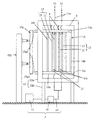
- FIG. 10 is a structural view seen from the front showing Embodiment 3 of the plasma processing apparatus of the present invention.
- the plasma processing apparatus according to the third embodiment is a vertically parallel type etching plasma processing apparatus, in which the first electrode 1 that is an anode electrode is grounded, and the second electrode 2 that is a cathode electrode is connected to the power supply unit E. Except for this, the configuration is generally the same as in the first embodiment.
- the left end surface of the first electrode 1 is connected to the grounding member 8 described in the first embodiment (see FIGS. 1 and 4).
- the gas introduction pipe as the gas introduction part 1a connected to the first electrode 1 is flexible and connected to the first electrode 1 as in the first embodiment.
- the grounding member 8 is also flexible.
- FIG. 10 the same components as those shown in FIGS. 1 to 8 are denoted by the same reference numerals.
- the reaction gas G2 that is an etching gas obtained by diluting a fluorine-based gas with an inert gas such as argon is supplied with the first electrode 1 and the second electrode at a predetermined flow rate and pressure.
- a glow discharge region plasma discharge region
- the substrate for example, silicon substrate
- the optimum inter-electrode distance is usually larger than the minimum inter-electrode distance A at the time of film formation.
- a wide inter-electrode plasma etching process in which the wide inter-electrode distance is set to 15 to 30 mm is appropriate. is there.
- the plasma etching process between narrow electrodes set to the minimum inter-electrode distance A is possible, since the inter-electrode distance becomes narrow, it is necessary to increase the pressure in the reaction chamber R to a pressure optimal for etching.
- the fourth embodiment (not shown) is a vertically parallel etching plasma processing apparatus similar to the third embodiment, and the first electrode fixing piece and the second electrode fixing piece are integrally formed as in the second embodiment.
- the first electrode is placed on the fixed piece, and the second electrode is pressed against the lower surface of the fixed piece by the ascending operation of the moving mechanism to determine the minimum distance A between the electrodes.
- the distance between the electrodes is wider than the minimum distance A between electrodes (see FIG. 9).
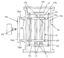
- FIG. 11 is a configuration diagram viewed from the front showing Embodiment 5 of the plasma processing apparatus of the present invention
- FIG. 12 is an internal configuration diagram viewed from one side of Embodiment 5 of the present invention
- FIG. It is an internal block diagram seen from the upper part of Embodiment 5,
- FIG. 14 is explanatory drawing which shows the state which the 1st electrode in Embodiment 5 of this invention moves to a horizontal direction.
- FIGS. 11 to 14 the same components as those shown in FIGS. 1 to 8 are denoted by the same reference numerals.
- the plasma processing apparatus of the fifth embodiment is for film formation and is mainly different from the first embodiment (upper and lower parallel type) in that it is a left and right parallel type
- the first electrode 11 and the second electrode are the same as in the first embodiment.
- a plurality of sets of discharge units 13 composed of the electrodes 12, a chamber C2, a support unit 14, a moving mechanism 15, a power supply unit E, a gas introduction unit 11a, and an exhaust unit (not shown) are provided.
- the configuration of the support portion 14 and the moving mechanism 15 is different from that of the first embodiment. Different.
- the first electrode 11 is a cathode electrode
- the second electrode 12 is an anode electrode
- the configuration of these electrodes is the same as that of the first embodiment.
- the substrate S1 (see FIG. 14) that is an object to be processed is installed on the discharge surface of the second electrode 12 and the discharge units 13 are arranged in the reaction chamber R in two rows on the left and right is illustrated.
- the number of discharge portions 13 is not limited to two, and the present invention can be applied to one or three or more.
- the points of the fifth embodiment different from the first embodiment will be mainly described.
- the support portion 14 is arranged at the vertex position of a quadrangle when viewed from the side and extends in parallel in the left-right direction, and a frame body 14b that connects the vicinity of the left and right end portions of the four beam members 14a to each other.
- the frame body 14b is formed by combining four straight members. The left end of each beam member 14a is fixed to the left inner wall surface of the chamber C2, the two lower beam members 14a are fixed to the support base 14c, and each support base 14c is fixed to the inner surface of the bottom wall of the chamber C2. .
- the fixed piece 17 includes a first portion 17a having a thickness equal to the minimum interelectrode distance A between the first electrode 11 and the second electrode 12, and a second portion 17b having a thickness equal to or greater than the thickness of the second electrode 12. It has.
- the fixing piece 17 holds the second electrode 12 in the left and right two rows of the discharge portions 3 at the second portion 17b and holds the substrate S1 at the first portion 17a in a state of being in contact with the discharge surface of the second electrode 12.
- the minimum distance A between the first electrode 11 and the second electrode 12 is determined by the first portion 17a.
- four fixing pieces 17 are fixed to the four beam members 14a, respectively.
- the distance B between the discharge sections 13 is set to an interval that is at least twice the minimum electrode distance A (B / A ⁇ 2).
- the moving mechanism 15 includes four beam members 15a that are arranged at the vertex positions of a quadrangle when viewed from the side and extend in parallel in the left-right direction, and a frame body 15b that connects the vicinity of the left and right ends of the four beam members 15a to each other.
- a plurality of movable pieces 15c attached inward to the four beam members 15a and two beam members 15a arranged at the front and back of the beam member 15a are slidable horizontally on the inner surface of the bottom wall of the chamber C2.
- the frame 15b is formed by combining four straight members.
- the moving structure in which the four beam members 15a and the frame body 15b are connected to each other is the interior of the support structure in which the four beam members 14a and the frame body 14b of the support portion 14 are connected to each other.
- the space is formed in such a size that it can reciprocate in the horizontal direction.
- the two support guide rails 15 are fixed to the inner surface of the bottom wall of the chamber C2 between the two support bases 14c.
- the movable piece 15 c has a shape having a recess that fits with the upper end or the lower end of the first electrode 11. In order to hold one first electrode 11 vertically, the four movable pieces 15c are fixed to the four beam members 15a, respectively. In addition, between the four movable pieces 15c holding one first electrode 11 and the four movable pieces 15c holding the other first electrode 11, the distance between the two discharge portions 13 is the minimum inter-electrode distance at the same time. An interval that can be set to A is set.
- the reciprocating drive unit 15f is a hydraulic cylinder mechanism including two hydraulic cylinders.
- a support for supporting each hydraulic cylinder is erected on the floor of the installation site so that each hydraulic cylinder expands and contracts in the horizontal direction.
- the connecting portion 15g includes a connecting plate 15g1 fixed to the ends of the telescopic rods of the two hydraulic cylinders, and a connecting member 15g2 for connecting the connecting plate 15g1 and the left ends of the four beam members 15a, and a reciprocating drive portion 15f.
- the left and right horizontal movements are synchronously transmitted to the four beam members 15a and the movable pieces 15c attached thereto via the connecting plate 15g1 and the four connecting members 15g2.
- the four connecting members 15g2 of the connecting portion 15g are inserted through four insertion holes formed in the left side wall of the chamber C2 so as to be movable in the left-right direction. Further, a cylindrical guide member 15h that is in communication with the four insertion holes and guides each connection member 15g2 is attached to the left side wall of the chamber C2, and is connected between the insertion hole and the connection member 15g2 and to the guide member 15h. The gap between the members 15g2 is sealed with a heat-resistant sealing material.
- the chamber C2 includes a metal box-shaped main body C2a and a metal leg C2b that supports the main body C2a on the floor of the installation place.
- the second electrode 12 has two conductive properties. It is grounded through the grounding member 8 and the metal chamber C2.
- the gas introduction part (gas introduction pipe) 11 a is connected to the upper end of each first electrode 11.
- the power supply unit E has the same configuration as that of the first embodiment.
- since the first electrode 11 is moved in the left-right direction by the moving mechanism 15, at least the connection side portion of the gas introduction part 11 a connected to the first electrode 1 and the power feeding cable e ⁇ b> 3 moves the first electrode 11. It is flexible so that it can accept and follow.
- the feeding position of the first electrode 11 is the center position in the front-rear direction of the lower end surface of the first electrode 11.
- the grounding location of the second electrode 12 is positioned on both sides of the center in the front-rear direction of the upper end surface of the second electrode 12.
- the movable piece 15c at the extension limit position of the reciprocating drive unit shown in FIG. The first electrode 11 is lightly pressed against the fixed piece 17 and stopped when pressed.
- the minimum interelectrode distance A is determined, and the narrow interelectrode plasma processing is enabled (see FIG. 14B).
- the first electrode 11 is separated from the second electrode 12 by the horizontal movement of the moving mechanism 15 in the right direction from the state of FIG.
- the substrate S1 can be easily installed, or the substrate S1 can be easily taken out from the second electrode 12.
- the movable piece 15c moves to the right by a predetermined distance, or from the state of FIG.
- the movable piece 15c moves to the left by a predetermined distance to move the first electrode 11. Is stopped before abutting against the fixed piece 17, a wide inter-electrode distance wider than the minimum inter-electrode distance A is determined, and the wide inter-electrode plasma processing becomes possible.
- the film forming plasma processing apparatus of the fifth embodiment is also adjusted to the minimum inter-electrode distance A according to the purpose of the plasma processing as in the first embodiment, and then the first electrode 11 and the second electrode 12 are adjusted.
- a plasma treatment step between the narrow electrodes in which plasma discharge is performed in the first reactive gas see FIG. 14B
- Either one of the wide electrode plasma processing steps for performing plasma discharge in the second reaction gas between the second electrodes 12 is performed, or the narrow electrode plasma processing step and the wide electrode plasma processing step are performed in any order.
- a continuous plasma treatment method can be implemented.
- the fixed piece 17 to which the first electrode 11 is pressed is formed of a metal material having impact resistance, and examples of such a metal material include iron-chromium metal.
- the material of the beam member 15a and the connecting member 15g2 may be either conductive or insulating, but from the viewpoint of workability and heat resistance, for example, a metal material of stainless steel or aluminum alloy is preferable.
- the movable piece 15c is preferably composed of an insulating material such as a metal oxide such as alumina or zirconia or a ceramic so that no current flows from the first electrode 11 to the beam member 15a via the movable piece 15c.
- zirconia having low thermal conductivity is configured to be interposed between the first electrode 11 and the beam member 15a. If an insulating material having a low thermal conductivity is interposed between the first electrode 11 and the beam member 15a, the heat of the first electrode 11 supported by the movable piece 15c becomes difficult to be transmitted to the beam member 15a. The elongation due to the thermal expansion of the member 15a can also be suppressed. Further, at least a portion of the movable piece 15c that is in contact with the first electrode 1 is preferably formed from a metal material having impact resistance. Examples of such a metal material include iron-chromium metal.
- the beam member 14a and the beam member 15a receive thermal radiation from the plasma and thermally expand to slightly extend. Therefore, it is preferable that the thermal expansion coefficients of the beam member 14a and the beam member 15a are the same.
- the beam member 14a and the beam member 15a are preferably formed of the same material, and both have a thickness and a shape. Are more preferably the same member.
- the distance from the plasma discharge region to the beam member 14a between the first electrode 11 and the second electrode 12, and the beam discharge from the plasma discharge region. The distance to the member 15a is substantially the same.
- the extension amount of the beam member 14a of the support structure and the extension amount of the beam member 15a of the moving structure at the time of the plasma processing are equal, and therefore the first electrode 11 is moved by the movable piece 15c of the moving mechanism 15.
- fluctuations in a predetermined interelectrode distance can be suppressed.
- the first electrode 11 held by the movable piece 15c is continuously brought into pressure contact with the fixed piece 17 by the reciprocating drive unit 15f during the plasma processing step, as in the first embodiment. There is no concern about fluctuations in the distance between the electrodes caused by elongation of the member due to excessive heat.
- the configuration in which the roller 15e is provided on the lower beam member 15a of the moving structure to run on the support guide rail 15d is illustrated.
- the beam member 15a is provided with a plurality of rollers on the support guide rail 15d. You may make it run.
- FIG. 15 is a configuration diagram seen from the front showing Embodiment 6 of the plasma processing apparatus of the present invention.
- the plasma processing apparatus according to the sixth embodiment is a left-right parallel type etching plasma processing apparatus, in which the first electrode 11 that is an anode electrode is grounded, and the second electrode 12 that is a cathode electrode is connected to the power supply unit E. Except for this, the configuration is generally the same as that of the fifth embodiment.
- the upper end surface of the first electrode 11 is connected to the grounding member 8 that grounds the second electrode 12 in the fifth embodiment (see FIG. 12).
- the gas introduction tube as the gas introduction portion 11a connected to the first electrode 11 has flexibility in the same manner as in the fifth embodiment.
- the grounding member 8 connected to the one electrode 11 is also flexible.
- the grounding member 8 that connects the box-shaped main body C1a of the chamber C1 and the first electrode 1 can be a flexible metal net member.
- FIG. 15 the same components as those shown in FIGS. 11 to 14 are denoted by the same reference numerals.
- a substrate for example, a silicon substrate installed along the second electrode 12 can be etched in the same manner as in the third and fourth embodiments.
- the optimum inter-electrode distance is usually larger than the minimum inter-electrode distance A during film formation, for example, a wide inter-electrode plasma etching process in which the wide inter-electrode distance is set to 15 to 30 mm. Is appropriate.
- the plasma etching process between narrow electrodes set to the minimum inter-electrode distance A is possible, since the inter-electrode distance becomes narrow, it is necessary to increase the pressure in the reaction chamber R to a pressure optimal for etching.
Landscapes
- Chemical & Material Sciences (AREA)
- Engineering & Computer Science (AREA)
- Physics & Mathematics (AREA)
- Plasma & Fusion (AREA)
- Analytical Chemistry (AREA)
- Materials Engineering (AREA)
- Chemical Kinetics & Catalysis (AREA)
- Mechanical Engineering (AREA)
- Metallurgy (AREA)
- Organic Chemistry (AREA)
- General Chemical & Material Sciences (AREA)
- Chemical Vapour Deposition (AREA)
- Drying Of Semiconductors (AREA)
- Plasma Technology (AREA)
Abstract
反応室と、反応室に反応ガスを導入するガス導入部と、反応室から反応ガスを排気する排気部と、反応室内に対向状に配置されかつ反応ガス中でプラズマ放電させる平板状の第1電極および第2電極と、第1電極または第2電極を支持または固定して対向方向に移動可能とする移動機構と、第1電極と第2電極の少なくとも一方を支持または固定する固定片とを備え、第1電極または第2電極が移動機構により移動され、かつ第1電極および第2電極の周縁部が固定片と当接することにより、第1電極と第2電極との最小電極間距離が決定できるプラズマ処理装置。
Description
本発明は、プラズマ処理装置およびそれを用いたプラズマ処理方法に関し、詳しくは、電極間距離を調整可能な装置構造および処理方法に関する。
平行平板型のプラズマ処理装置は、カソード電極とアノード電極のうちの一方に被処理物である基板が設置され、反応ガス雰囲気下で電極間にプラズマ放電を起こして基板表面をプラズマ処理する装置である。
プラズマを安定的に発生させるには、基板とそれに対向する電極との間の放電ギャップ長の管理が重要であるため、従来のプラズマ処理装置ではカソード電極とアノード電極が固定されることによって電極間距離(例えば5~30mm程度)が一定に維持されている。
プラズマを安定的に発生させるには、基板とそれに対向する電極との間の放電ギャップ長の管理が重要であるため、従来のプラズマ処理装置ではカソード電極とアノード電極が固定されることによって電極間距離(例えば5~30mm程度)が一定に維持されている。
また、従来のプラズマ処理装置は電極間距離を調整できないため、狭い電極間への基板の設置または取り出しが困難であることや、電極に付着した異物の除去が困難であるという不具合があり、そのため、上部電極を下部電極に対して水平平行方向にスライドさせることによりこれらの不具合を解消するプラズマ処理装置が提案されている(例えば、特許文献1参照)。
このスライド式プラズマ処理装置は、メインベース上に取り付けられた下部電極および2本のリニアガイドと、下部電極を跨ぐようにして各リニアガイド上に載置されたスライド部材と、下部電極と対向するようにしてスライド部材にボルトにて取り付けられた上部電極と、スライド部材および上部電極を下部電極に対して水平平行移動させるボールネジ機構とを備えている。また、このスライド式プラズマ処理装置において、上部電極は、基板の種類や厚さに応じて電極間距離を調整できるように隙間調整用ネジまたはスペーサを有する調整機構を介してスライド部材に取り付けられている。
このスライド式プラズマ処理装置は、メインベース上に取り付けられた下部電極および2本のリニアガイドと、下部電極を跨ぐようにして各リニアガイド上に載置されたスライド部材と、下部電極と対向するようにしてスライド部材にボルトにて取り付けられた上部電極と、スライド部材および上部電極を下部電極に対して水平平行移動させるボールネジ機構とを備えている。また、このスライド式プラズマ処理装置において、上部電極は、基板の種類や厚さに応じて電極間距離を調整できるように隙間調整用ネジまたはスペーサを有する調整機構を介してスライド部材に取り付けられている。
また、電極間距離を調整できる別のプラズマ処理装置としては、下部電極に対して上部電極が昇降移動する昇降式プラズマ装置が提案されている(例えば、特許文献2参照)。
この昇降式プラズマ装置は、上部電極を上下移動可能に支持する2本のリニアガイドと、上部電極の一端面に連結された可動片と、可動片を介して上部電極を上下移動させるボールネジ機構とを備えている。
この昇降式プラズマ装置は、上部電極を上下移動可能に支持する2本のリニアガイドと、上部電極の一端面に連結された可動片と、可動片を介して上部電極を上下移動させるボールネジ機構とを備えている。
しかしながら、前記スライド式プラズマ処理装置では、レールを敷設するためのメインベースのサイズが下部電極のサイズよりも大きいため、装置の設置面積が大幅に増加してしまうという新たな問題が生じる。また、上部電極とスライド部材とは4箇所がボルトおよび調整機構にて連結されているため、4箇所の電極間距離を同等にかつ迅速に手作業で調整することは困難である。
また、前記昇降式プラズマ処理装置において、電極間距離はボールネジ機構の移動精度に依存するため、電極間距離が小さい場合には、高精度のボールネジ機構が必要となる。また、電極の放電面積が大きくなった場合、ボールネジ機構を複数ヶ所に設け、それぞれを制御する必要があるため、装置の構成が複雑になるといった問題がある。
また、前記昇降式プラズマ処理装置において、電極間距離はボールネジ機構の移動精度に依存するため、電極間距離が小さい場合には、高精度のボールネジ機構が必要となる。また、電極の放電面積が大きくなった場合、ボールネジ機構を複数ヶ所に設け、それぞれを制御する必要があるため、装置の構成が複雑になるといった問題がある。
本発明は、上述の課題に鑑みなされたものであり、簡素な構造でありながら高精度に電極間距離を調整することができるプラズマ処理装置およびそれを用いたプラズマ処理方法を提供することを目的とする。
かくして、本発明によれば、反応室と、反応室に反応ガスを導入するガス導入部と、反応室から反応ガスを排気する排気部と、反応室内に配置されかつ反応ガス中でプラズマ放電させる平行平板状の第1電極および第2電極と、第1電極または第2電極を支持または固定して対向方向に移動可能とする移動機構と、第1電極と第2電極の少なくとも一方を支持または固定する固定片とを備え、第1電極または第2電極が前記移動機構により移動され、かつ第1電極および第2電極の周縁部が前記固定片と当接することにより、第1電極と第2電極との最小電極間距離が決定できるプラズマ処理装置が提供される。
かくして、本発明によれば、反応室と、反応室に反応ガスを導入するガス導入部と、反応室から反応ガスを排気する排気部と、反応室内に配置されかつ反応ガス中でプラズマ放電させる平行平板状の第1電極および第2電極と、第1電極または第2電極を支持または固定して対向方向に移動可能とする移動機構と、第1電極と第2電極の少なくとも一方を支持または固定する固定片とを備え、第1電極または第2電極が前記移動機構により移動され、かつ第1電極および第2電極の周縁部が前記固定片と当接することにより、第1電極と第2電極との最小電極間距離が決定できるプラズマ処理装置が提供される。
また、本発明の別の観点によれば、前記プラズマ処理装置を用いて前記第1電極または第2電極に設置された基板の表面をプラズマ処理する方法であって、プラズマ処理の目的に応じて、前記移動機構の動作によって、第1電極と第2電極の間を前記最小電極間距離に調整した後、第1電極と第2電極の間に反応ガス中でプラズマ放電させる狭電極間プラズマ処理工程と、第1電極と第2電極の間を前記最小電極間距離よりも広い広電極間距離に調整した後、第1電極と第2電極の間に反応ガス中でプラズマ放電させる広電極間プラズマ処理工程のいずれか一方を行うか、或いは前記狭電極間プラズマ処理工程と前記広電極間プラズマ処理工程を任意の順で連続的に行うプラズマ処理方法が提供される。
本発明のプラズマ処理装置は、第1電極または第2電極を支持または固定して対向方向に移動可能とする移動機構と、第1電極と第2電極の少なくとも一方を支持または固定する固定片とを備えているため、第1電極または第2電極が前記移動機構により移動され、かつ第1電極および第2電極の周縁部が前記固定片と当接することにより、第1電極と第2電極との最小電極間距離が容易に決定される。さらに、移動機構によって第1電極と第2電極を相対的に離間する方向に移動させることができるため、第1電極と第2電極との間を任意の電極間距離に広げることができる。
したがって、第1電極と第2電極との間を最小電極間距離に設定した狭電極間プラズマ処理と、第1電極と第2電極との間を最小電極間距離よりも広い電極間距離に設定した広電極間プラズマ処理とのいずれか一方の処理または任意の順で連続的に両方の処理を行うこと(プラズマ処理方法)が可能となる。さらに、電極間距離を広くすることにより、電極間に被処理物である基板の設置および電極間からの基板の取り出しを容易に行うことができる。
したがって、第1電極と第2電極との間を最小電極間距離に設定した狭電極間プラズマ処理と、第1電極と第2電極との間を最小電極間距離よりも広い電極間距離に設定した広電極間プラズマ処理とのいずれか一方の処理または任意の順で連続的に両方の処理を行うこと(プラズマ処理方法)が可能となる。さらに、電極間距離を広くすることにより、電極間に被処理物である基板の設置および電極間からの基板の取り出しを容易に行うことができる。
本発明のプラズマ処理装置は、反応室と、反応室に反応ガスを導入するガス導入部と、反応室から反応ガスを排気する排気部と、反応室内に配置されかつ反応ガス中でプラズマ放電させる平行平板状の第1電極および第2電極と、第1電極または第2電極を支持または固定して対向方向に移動可能とする移動機構と、第1電極と第2電極の少なくとも一方を支持または固定する固定片とを備え、第1電極または第2電極が前記移動機構により移動され、かつ第1電極および第2電極の周縁部が前記固定片と当接することにより、第1電極と第2電極との最小電極間距離が決定できる。
つまり、このプラズマ処理装置は、平行平板型の第1電極および第2電極のうちの一方の電極は支持または固定され、他方の電極は移動機構によって対向方向に移動可能に支持または固定されている。したがって、移動機構に支持または固定された電極を移動させることにより電極間距離を調整することができると共に、両方の電極を固定片と当接させることによって両方の電極を最小電極間距離まで接近させることができる。
さらに、このプラズマ処理装置は、第1電極と第2電極との間隔を最小電極間距離に設定した状態でのプラズマ処理(狭電極間プラズマ処理工程)と、最小電極間距離よりも広い電極間距離に設定した状態でのプラズマ処理(広電極間プラズマ処理工程)の一方または両方を任意に行うことができる。それに加え、第1・第2電極を相対的に移動させて電極間を広くすることにより、電極間への基板の搬入、電極間からの基板の搬出、電極放電面のクリーニングが容易となる。
さらに、このプラズマ処理装置は、第1電極と第2電極との間隔を最小電極間距離に設定した状態でのプラズマ処理(狭電極間プラズマ処理工程)と、最小電極間距離よりも広い電極間距離に設定した状態でのプラズマ処理(広電極間プラズマ処理工程)の一方または両方を任意に行うことができる。それに加え、第1・第2電極を相対的に移動させて電極間を広くすることにより、電極間への基板の搬入、電極間からの基板の搬出、電極放電面のクリーニングが容易となる。
このプラズマ処理装置は、第1電極および第2電極からなる平行平板型の放電部(電極体)の1組または複数組を上下方向に並べた上下並列タイプと、平行平板型の放電部の1組または複数組を左右方向に並列した左右並列タイプの両方に適用できる。上下並列タイプでは第1・第2電極は水平状に配置され、左右並列タイプでは第1・第2電極は垂直状に配置される。
また、このプラズマ処理装置は、成膜用とエッチング用の両方に適用可能である。
また、このプラズマ処理装置は、成膜用とエッチング用の両方に適用可能である。
本発明において、前記固定片は、第1電極および第2電極の周縁部と当接して最小電極間距離を決定するように反応室内に設けられていれば、取付方法は特に限定されるものではない。例えば、反応室内に第1電極および第2電極の少なくとも一方を支持する支持部を設け、支持部に固定片を取り付ける、あるいは反応室を構成するチャンバーの内壁面またはチャンバーのフレームに固定片を取り付けることができる。
反応室内で第1電極と第2電極の一方を移動させるため、移動させる電極が給電ケーブル、接地部材またはガス導入管等の接続部材と接続される場合は、可撓性を有する接続部材を選択し、接続部材が電極の動きを許容しかつ追随できるようにする必要がある。チャンバー内壁面と電極周縁部との間の間隔にゆとりを持たせれば、接続部材が電極の動きを許容しかつ追随でき易くなる。この場合、反応室内に支持部を設け、支持部に固定片を取り付けることが好ましく、支持部としては、少なくとも固定片を取り付けるための支柱部材、梁部材、枠部材等の支持部材が反応室内に設けられていればよい。
反応室内で第1電極と第2電極の一方を移動させるため、移動させる電極が給電ケーブル、接地部材またはガス導入管等の接続部材と接続される場合は、可撓性を有する接続部材を選択し、接続部材が電極の動きを許容しかつ追随できるようにする必要がある。チャンバー内壁面と電極周縁部との間の間隔にゆとりを持たせれば、接続部材が電極の動きを許容しかつ追随でき易くなる。この場合、反応室内に支持部を設け、支持部に固定片を取り付けることが好ましく、支持部としては、少なくとも固定片を取り付けるための支柱部材、梁部材、枠部材等の支持部材が反応室内に設けられていればよい。
移動機構は、第1電極または第2電極が支持または固定されて対向方向に移動できるものであればその構成は特に限定されず、第1電極と第2電極のどちらを移動させるものであってもよい。ただし、移動機構は、プラズマ処理装置が上下並列タイプの場合は電極を上下方向に移動させるように構成され、プラズマ処理装置が左右並列タイプの場合は電極を水平方向に移動させるように構成される。
電極を上下方向または水平方向に移動させる移動機構としては、例えば、油圧シリンダ機構、ボールネジ機構、これらを動力源として用いたリンク機構等が挙げられ、中でも重量物の昇降を高精度に行うことができる油圧シリンダ機構が好ましい。
以下、本発明に係る上下並列タイプと左右並列タイプのプラズマ処理装置の実施形態について、図面を参照しながら詳しく説明する。
電極を上下方向または水平方向に移動させる移動機構としては、例えば、油圧シリンダ機構、ボールネジ機構、これらを動力源として用いたリンク機構等が挙げられ、中でも重量物の昇降を高精度に行うことができる油圧シリンダ機構が好ましい。
以下、本発明に係る上下並列タイプと左右並列タイプのプラズマ処理装置の実施形態について、図面を参照しながら詳しく説明する。
(実施形態1:上下並列タイプ)
図1は本発明のプラズマ処理装置の実施形態1を示す正面から見た構成図であり、図2は本発明の実施形態1の一側面から見た内部構成図であり、図3は図2における電極が無い状態の内部構成図であり、図4は本発明の実施形態1の上方から見た内部構成図であり、図5は本発明の実施形態1における固定片と支持片との位置関係を説明する図であり、図6は本発明の実施形態1における第1電極が昇降する状態を示す説明図である。
図1は本発明のプラズマ処理装置の実施形態1を示す正面から見た構成図であり、図2は本発明の実施形態1の一側面から見た内部構成図であり、図3は図2における電極が無い状態の内部構成図であり、図4は本発明の実施形態1の上方から見た内部構成図であり、図5は本発明の実施形態1における固定片と支持片との位置関係を説明する図であり、図6は本発明の実施形態1における第1電極が昇降する状態を示す説明図である。
このプラズマ処理装置は上下並列タイプであり、反応室Rを構成するチャンバーC1と、反応室Rに矢印で示す反応ガスG1を導入するガス導入部1aと、反応室Rから反応ガスG1を排気する排気部6と、反応室R内に水平に対向して配置されかつ反応ガスG1中でプラズマ放電させる平板状の第1電極1および第2電極2からなる放電部3と、第1電極1に電力を供給する電源部Eと、第2電極2を接地する接地部材8と、反応室R内に設けられて第1・第2電極1、2を水平状に支持する支持部4と、支持部4に取り付けられた固定片7a、7bと、第1電極1を対向方向に移動させる移動機構5とを備える。
実施形態1では、第1電極1がカソード電極であり、第2電極がアノード電極であり、第2電極2上に被処理物である基板S1(図6参照)が設置され、基板S1の表面に所定の膜を成膜するプラズマ処理装置の場合を例示している。また、実施形態1では、放電部3が上下2段で反応室内Rに配置された場合を例示しているが、放電部3の数は2つに限定されるものではなく、1つまたは3つ以上でもよい。
チャンバーC1は、金属製の箱型本体部C1aと、本体部C1aを設置場所の床面上に支持する金属製の脚部C1bとを備えている。第2電極2は、2本の導電性接地部材8および金属製のチャンバーC1を介して接地されている。
排気部6としては、真空ポンプ6a、真空ポンプ6aと反応室Rとを接続する排気管6bおよび排気管6bにおける反応室Rと真空ポンプ6aとの間に配置された圧力制御器6cとを備える。
排気部6としては、真空ポンプ6a、真空ポンプ6aと反応室Rとを接続する排気管6bおよび排気管6bにおける反応室Rと真空ポンプ6aとの間に配置された圧力制御器6cとを備える。
電源部Eは、例えば、AC1.00MHz~60MHzの周波数で10W~100kWの電力、具体的には、13.56MHz~60MHzで10W~10kWの電力を発生して各第1電極1に供給するプラズマ励起電源である。電源部Eは、高周波発生器e1と、各第1電極1に均等な電力を供給するためのインピーダンス整合器e2と、これらを各第1電極1の給電箇所に接続する給電ケーブルe3とを備え、図示しない増幅器をさらに備えていてもよい。
実施形態1の場合、後述する移動機構5によって第1電極1が昇降するため、第1電極1と接続される給電ケーブルe3の少なくとも接続側部分は、第1電極1の昇降動作を許容しかつ追随できるよう可撓性を有している。例えば、チャンバーC1の箱型本体部C1aと第1電極1との間部分の給電ケーブルは、可撓性を有する金属製網部材とすることができる。
なお、実施形態1の場合、第1電極1の給電箇所は、第1電極1の右端面の前後方向中央位置とされている。また、第2電極2の接地箇所は、第2電極2の左端面の前後方向中央の両側位置とされている。
実施形態1の場合、後述する移動機構5によって第1電極1が昇降するため、第1電極1と接続される給電ケーブルe3の少なくとも接続側部分は、第1電極1の昇降動作を許容しかつ追随できるよう可撓性を有している。例えば、チャンバーC1の箱型本体部C1aと第1電極1との間部分の給電ケーブルは、可撓性を有する金属製網部材とすることができる。
なお、実施形態1の場合、第1電極1の給電箇所は、第1電極1の右端面の前後方向中央位置とされている。また、第2電極2の接地箇所は、第2電極2の左端面の前後方向中央の両側位置とされている。
各第1電極(カソード電極)1は、長方形であり、ステンレス鋼やアルミニウム合金などから作製される。各第1電極1の寸法は、成膜される基板S1の寸法に合わせて適当な値に設定され、第2電極2よりも僅かに大きい平面サイズおよび第2電極2と同じ厚みで設計されることができる。
各第1電極1は、内部が空洞であると共に、対となる第2電極2に面するプラズマ放電面には多数の貫通穴が穴明け加工により明けられている。この穴明け加工は、例えば、直径0.1mm~2mmの円形穴を数mm~数cmピッチで行うことができる。
また、各第1電極1の一端面には、ガス導入部1aとしてのガス導入管が接続されている。図示しないガス供給源とガス導入部1aとは接続パイプにて接続されており、反応ガスG1がガス供給源から第1電極2の内部に供給され、多数の貫通穴から基板S1の表面に向かって噴出する。また、上述のように第1電極1が昇降するため、第1電極1と接続されるガス導入管1aの少なくとも接続側部分は、第1電極1の昇降動作を許容しかつ追随できるよう可撓性を有している。例えば、チャンバーC1の箱型本体部C1aと第1電極1との間部分のガス導入管は、可撓性を有するフッ素系樹脂管とすることができる。なお、原料ガスとしては、例えば、H2で希釈したSiH4(モノシラン)ガスが使用される。
各第2電極2は、長方形であり、内部に図示しないヒータを有すると共に、上面に基板S1が設置され、プラズマ放電下の成膜時に基板S1を加熱する。なお、基板S1は、シリコン基板やガラス基板などが一般的であるが、特にこれらに限定されるものではない。
また、各第2電極2は、ステンレス鋼、アルミニウム合金、カーボンなどの、導電性および耐熱性を備えた材料で製作されている。
各第2電極2の寸法は、薄膜を形成するための基板S1の寸法に合わせて適当な値に決定されている。例えば、基板S1の寸法900~1200mm×400~900mmに対して、第2電極2の寸法は1000~1500mm×600~1000mmとされる。ただし、後で詳しく説明する支持片5cが下降する際に第2電極2に衝突しないように、第2電極2の左右方向の長さは第1電極1の左右方向の長さよりも短く設定されている(図1および図6参照)。
各第2電極2に内蔵されたヒータは、第2電極2を室温~300℃程度に加熱制御するものであり、例えば、アルミニウム合金製の筒体内にシースヒータのような密閉型加熱装置と熱電対などの密閉型温度センサとを内蔵したものを用いることができる。
支持部4は、反応室R内における第1電極1および第2電極2の周囲に配置された複数本の支持用支柱4aと、複数本の支持用支柱4aを連結する枠体4bと、各支持用支柱4aに取り付けられた第1電極用固定片7aおよび第2電極用固定片7bとが一体化された支持構造体である。以下、第1電極用固定片7aおよび第2電極用固定片7bを、第1固定片7aおよび第2固定片7bと称するか、あるいはこれらを統合して固定片7a、7bと称する場合がある。
具体的には、各電極1、2の4つの角部付近に配置されるように4本の支持用支柱4aがチャンバーC1の底壁内面に固定されている。そして、4本の支持用支柱4aの上端が四角形の枠体4bにて連結されている。また、各支持用支柱4aの所定高さ位置の2箇所に、第1固定片7aおよび第2固定片7bがそれぞれ内向きに取り付けられている。なお、枠体4bは、4本のストレートな部材を組み合わせてなる。
具体的には、各電極1、2の4つの角部付近に配置されるように4本の支持用支柱4aがチャンバーC1の底壁内面に固定されている。そして、4本の支持用支柱4aの上端が四角形の枠体4bにて連結されている。また、各支持用支柱4aの所定高さ位置の2箇所に、第1固定片7aおよび第2固定片7bがそれぞれ内向きに取り付けられている。なお、枠体4bは、4本のストレートな部材を組み合わせてなる。
つまり、上下の放電部3の各第1電極1を水平状に支持する8つの第1固定片7aと、上下の放電部3の各第2電極2を水平状に支持する8つの第2固定片7bとが、4本の支持用支柱4aの所定高さ位置に取り付けられている。このとき、図6(B)に示すように、各段の第1・第2固定片7a、7bは、各放電部3における第1電極1と第2電極2との間の最小電極間距離Aが所定距離となる高さ位置に配置されると共に、上段の第2固定片7bと下段の第1固定片7aは、上下の放電部3の間の放電部間距離Bが所定距離となる高さ位置に配置されている。また、第2電極2を支持する下の第2固定片7bは、第1電極1よりも左右方向の長さが短い第2電極2を支持できるように、上の第1固定片7aよりも内側へ長く形成されている。
ところで、反応室R内に複数組の放電部3が存在すると、各放電部3でのプラズマ放電が相互に干渉する場合がある。その原因は、特に、電源部Eと同一の電気系統を介してそれぞれ接続される放電部同士の放電部間距離Bに関係しており、放電部間距離Bが短くなると電力を均等に分岐できなくなり、その結果各プラズマ放電が干渉する。
このようなプラズマ放電の干渉を防止するため、本発明では、各放電部3における第1電極(カソード電極)1と第2電極(アノード電極)2との間の電極間距離Aに対して放電部間距離Bが2倍以上(B/A≧2)となるように設定されている。例えば、電極間距離Aは2~30mmに設定され、放電部間距離Bは4~60mm以上に設定される。なお、面内における電極間距離Aの精度は、数%以内であることが好ましく、1%以下であること特に好ましい。
このようなプラズマ放電の干渉を防止するため、本発明では、各放電部3における第1電極(カソード電極)1と第2電極(アノード電極)2との間の電極間距離Aに対して放電部間距離Bが2倍以上(B/A≧2)となるように設定されている。例えば、電極間距離Aは2~30mmに設定され、放電部間距離Bは4~60mm以上に設定される。なお、面内における電極間距離Aの精度は、数%以内であることが好ましく、1%以下であること特に好ましい。
支持用支柱4aの材料は、導電性と絶縁性のどちらでもよいが、加工性および耐熱性の観点から、例えば、ステンレス、もしくはアルミ合金等の金属材料が好ましい。
各固定片7a、7bは、第1電極1および第2電極2からの熱が各固定片7a、7bを介して支持用支柱4aへ伝わり難いように、例えば、アルミナ、ジルコニア等の金属酸化物またはセラミック等の絶縁材料で構成されていることが好ましく、特に、熱伝導率が低いジルコニアが第1電極1および第2電極と支持用支柱4aの間に介在するように構成されていることが好ましい。すなわち、固定片7a、7bの全てが絶縁材料で構成されていても良いが、一部が絶縁材料で構成されていても良い。このように絶縁材料が介在する構成とすれば、各固定片7a、7bにて支持された第1電極1および第2電極の熱が支持用支柱4aへ伝わり難くなり、支持用支柱4aの熱膨張による伸びを抑えることができる。
各固定片7a、7bは、第1電極1および第2電極2からの熱が各固定片7a、7bを介して支持用支柱4aへ伝わり難いように、例えば、アルミナ、ジルコニア等の金属酸化物またはセラミック等の絶縁材料で構成されていることが好ましく、特に、熱伝導率が低いジルコニアが第1電極1および第2電極と支持用支柱4aの間に介在するように構成されていることが好ましい。すなわち、固定片7a、7bの全てが絶縁材料で構成されていても良いが、一部が絶縁材料で構成されていても良い。このように絶縁材料が介在する構成とすれば、各固定片7a、7bにて支持された第1電極1および第2電極の熱が支持用支柱4aへ伝わり難くなり、支持用支柱4aの熱膨張による伸びを抑えることができる。
絶縁材料からなる絶縁部材を有してなる固定片7a、7bを金属材料からなる支持用支柱4aへ取り付ける場合、固定片7a、7bは、例えば図7(A)または図7(B)で図示したように構成されてもよい。
図7(A)の場合、固定片7aは、例えば、支持用支柱4aの所定高さ位置に溶接される金属製受け片7a1と、受け片7a1上に設置される絶縁部材7a2と、受け片7a1および絶縁部材7a2に形成された貫通孔に挿入されるボルト部材(図示省略)と、ボルト部材に螺合して絶縁部材7a2を受け片7a1に締め付けて固定するナット部材(図示省略)とから構成されることができる。なお、図7(A)では固定片7aのみを示したが、固定片7bも固定片7aと同様である。
図7(B)の場合、固定片7aは、図7(A)で示した第1電極1と当接する絶縁部材7a2上に、耐衝撃性を有する金属材料(例えば鉄クロム系金属)から形成された金属片7a3を載置し、前記ボルト・ナット結合により受け片7a1、絶縁部材7a2および金属片7a3を結合して構成されることができる。なお、図7(B)では固定片7aのみを示したが、固定片7bも固定片7aと同様である。
移動機構5は、反応室R内における第1電極1および第2電極2の周囲に配置された4本の昇降用支柱5aと、4本の昇降用支柱5aの上下2箇所を連結する枠体5bと、各固定片7a、7bと干渉しないように昇降用支柱5aまたは枠体5bに取り付けられた複数の支持片5cと、昇降駆動部5dと、昇降駆動部5dと昇降用支柱5aまたは枠体5bとを連結し昇降駆動部5dの昇降動作を伝達する連結部5eとを備える。
この移動機構5は、所定ストロークの上昇動作によって、第1固定片7a上の第1電極1を第2電極2から離間させ(図6(A)参照)、所定ストロークの下降動作によって、第1電極1を第1固定片7a上に載置する(図6(B)参照)ように構成されている。
図6(B)は、第1固定片7aに第1電極1が当接しかつ第2固定片7bに第2電極2が当接することにより、前記最小電極間距離Aが決定された状態を示している。
この移動機構5は、所定ストロークの上昇動作によって、第1固定片7a上の第1電極1を第2電極2から離間させ(図6(A)参照)、所定ストロークの下降動作によって、第1電極1を第1固定片7a上に載置する(図6(B)参照)ように構成されている。
図6(B)は、第1固定片7aに第1電極1が当接しかつ第2固定片7bに第2電極2が当接することにより、前記最小電極間距離Aが決定された状態を示している。
4本の昇降用支柱5aは、4本の支持用支柱4aの近傍に配置されている。さらに詳しくは、各昇降用支柱5aが2本の支持用支柱4aの間で、かつ各昇降用支柱5aから各電極までの距離が支持用支柱4aから各電極までの距離とほぼ等しくなるように配置されている。そして、4本の昇降用支柱5aの上部および下部が枠体5bにて相互に連結されている。なお、枠体5bは、4本のストレートな部材を組み合わせてなる。
また、支持片5cは、上下の放電部3の第1電極1を昇降可能なように、4本の昇降用支柱4aに2つずつ内向きに取り付けられている。また、支持片5cの内側への突出寸法は、支持片5cが下降した際に第2電極2と衝突しない長さに設定されている。このとき、図6(B)に示すように、昇降用支柱5aを下降させて最小電極間距離Aに設定された状態において、各昇降用支柱5aに対応する上下2つの支持片5cは、上下の放電部3の第2電極2の下面よりも僅かに(例えば5mm程度)下方に位置する。
なお、支持片5cを第2電極2の下面よりも下に下降させる理由は、放電部3のプラズマ放電領域に第1電極を支持していない支持片が存在すると、支持片がプラズマに干渉して放電空間に均一なプラズマを発生できなくなるからである。
昇降駆動部5dは、2つの油圧シリンダを備える油圧シリンダ機構であり、各油圧シリンダが上下方向に伸縮するよう設置場所の床面に固定されている。
連結部5eは、2つの油圧シリンダの伸縮ロッドの先端に固定された連結板5e1と、連結板5e1と4本の昇降用支柱5aの下端とを連結する連結支柱5e2とを備え、昇降駆動部5dの昇降動作を連結板5e1および4本の連結支柱5e2を介して4本の昇降用支柱5aおよびこれらに取り付けられた各支持片5cに同期的に伝達するように構成されている。なお、昇降駆動部5の上昇動作の限界は、上方の枠体5bが支持部4の上方の枠体4bに当たらない程度とされる。
連結部5eの4本の連結支柱5e2は、チャンバーC1の底壁の4箇所に形成された挿通孔を上下移動可能に挿通している。さらに、チャンバーC1の底壁には4つの挿通孔と連通して各連結支柱5e2をガイドする筒状のガイド部材5fが取り付けられており、挿通孔と連結支柱5e2の間およびガイド部材5fと連結支柱5e2の間の隙間は耐熱シール材にてシールされている。
昇降用支柱5aおよび連結支柱5e2の材料は、導電性と絶縁性のどちらでもよいが、加工性および耐熱性の観点から、例えば、ステンレス、もしくはアルミ合金等の金属材料が好ましい。
支持片5cは、第1電極1から電流が支持片5cを介して昇降用支柱5aへ流れないように、例えば、アルミナ、ジルコニア等の金属酸化物またはセラミック等の絶縁材料にて構成されることが好ましく、特に、熱伝導率が低いジルコニアが第1電極1と昇降用支柱5aの間に介在するように構成されていることが好ましい。第1電極1と昇降用支柱5aの間に熱伝導率が低い絶縁材料が介在すれば、支持片5cにて支持された第1電極1の熱が昇降用支柱5aへ伝わり難くなり、昇降用支柱5aの熱膨張による伸びを抑えることもできる。さらに、少なくとも支持片5cの第1電極1と当接する部分は、耐衝撃性を有する金属材料から形成されることが好ましく、このような金属材料としては、例えば鉄クロム系金属が挙げられる。
支持片5cは、第1電極1から電流が支持片5cを介して昇降用支柱5aへ流れないように、例えば、アルミナ、ジルコニア等の金属酸化物またはセラミック等の絶縁材料にて構成されることが好ましく、特に、熱伝導率が低いジルコニアが第1電極1と昇降用支柱5aの間に介在するように構成されていることが好ましい。第1電極1と昇降用支柱5aの間に熱伝導率が低い絶縁材料が介在すれば、支持片5cにて支持された第1電極1の熱が昇降用支柱5aへ伝わり難くなり、昇降用支柱5aの熱膨張による伸びを抑えることもできる。さらに、少なくとも支持片5cの第1電極1と当接する部分は、耐衝撃性を有する金属材料から形成されることが好ましく、このような金属材料としては、例えば鉄クロム系金属が挙げられる。
また、プラズマ処理時には、支持用支柱4aおよび昇降用支柱5aはプラズマからの輻射熱を受けて熱膨張し僅かに伸びる。したがって、支持用支柱4aと昇降用支柱5aの熱膨張率は同じであることが好ましく、そのために、支持用支柱4aと昇降用支柱5aは同じ材料にて形成されていることが好ましく、両者は各種寸法および形状も同一の同じ部材から構成されていることがさらに好ましい。さらには、支持用支柱4aおよび昇降用支柱5aが受ける輻射熱量を同じにするために、上述のように第1電極1と第2電極2の間のプラズマ放電領域から支持用支柱4aまでの距離と、プラズマ放電領域から昇降用支柱5aまでの距離とは同一に設定されている。
このようにすれば、プラズマ処理時の支持用支柱4aの伸び量と昇降用支柱5aの伸び量が同等となるため、移動機構5の支持片5cにて第1電極1を支持する上述の広電極間プラズマ処理工程において、所定の電極間距離の変動を小さく抑えることができる。なお、支持部4の第1・第2固定片7a、7bにて第1・第2電極1、2を支持する狭電極間プラズマ処理工程では、支持用支柱4の伸びによる最小電極間距離Aの変動はさらに小さいものとなる。
絶縁材料からなる絶縁部材を有してなる支持片5cを金属材料からなる昇降用支柱5aへ取り付ける場合、支持片5aは、例えば図8(A)または図8(B)で図示したように構成されてもよい。
図8(A)の場合、支持片5aは、図7(A)で説明した固定片7aと同様に、金属製受け片5c1と絶縁部材5c2とをボルト・ナット結合して構成される。
図8(B)の場合、支持片5aは、図7(B)で説明した固定片7aと同様に、絶縁部材5c2上に、耐衝撃性を有する金属材料(例えば鉄クロム系金属)から形成された金属片5c3を載置し、受け片5c1、絶縁部材5c2および金属片5c3をボルト・ナット結合して構成される。
図8(A)の場合、支持片5aは、図7(A)で説明した固定片7aと同様に、金属製受け片5c1と絶縁部材5c2とをボルト・ナット結合して構成される。
図8(B)の場合、支持片5aは、図7(B)で説明した固定片7aと同様に、絶縁部材5c2上に、耐衝撃性を有する金属材料(例えば鉄クロム系金属)から形成された金属片5c3を載置し、受け片5c1、絶縁部材5c2および金属片5c3をボルト・ナット結合して構成される。
このように構成された実施形態1の成膜用プラズマ処理装置によれば、昇降駆動部5dが伸長動作することによる移動機構5の上昇動作によって、図6(B)に示す最下位置の支持片5cが上昇して第1電極1を受け、さらに支持片5cが上昇することにより第1電極1が第2電極2から離間する(図6(A)参照)。この際、第2電極2、固定片7aおよび支持片5の寸法が上述のように設定されているため、支持片5cが第2電極2に衝突することはない。このように電極間距離が広がることにより、第2電極2上に基板S1を容易に設置する、あるいは第2電極2上から基板S1を容易に取り出すことができる。
また、図6(A)の状態から、昇降駆動部5dが短縮動作することによる移動機構5の下降動作によって、最上位置の支持片5cが下降して第1電極1が第1固定片7a上に載置され、これによって最小電極間距離Aが決定され、さらに支持片5cが第2電極2の下面よりも下に下降することによって、狭電極間プラズマ処理が可能となる。
また、図6(A)の状態から、最上位置の支持片5cが下降し、第1電極1が第1固定片7a上に載置される前に支持片5cの下降が停止することにより、あるいは図6(B)の状態から支持片5cが上昇して第1電極1を受け、支持片5cの上昇が最上位置に達する前に停止することにより、最小電極間距離Aよりも広い広電極間距離(例えば15~30mm程度)が決定され、広電極間プラズマ処理が可能となる。
すなわち、この成膜用プラズマ処理装置では、プラズマ処理の目的に応じて、最小電極間距離Aに調整した後、第1電極1と第2電極2の間に第1の反応ガス中でプラズマ放電させる狭電極間プラズマ処理工程と(図6(A)参照)、最小電極間距離Aよりも広い広電極間距離に調整した後、第1電極1と第2電極2の間に第2の反応ガス中でプラズマ放電させる広電極間プラズマ処理工程のいずれか一方を行うか、或いは狭電極間プラズマ処理工程と広電極間プラズマ処理工程を任意の順で連続的に行うプラズマ処理方法を実施することができる。
ここで、「プラズマ処理の目的に応じて」とは、成膜すべき膜の材料、膜の緻密度、基板S1の厚み等に対応するという意味である。
ここで、「プラズマ処理の目的に応じて」とは、成膜すべき膜の材料、膜の緻密度、基板S1の厚み等に対応するという意味である。
狭電極間プラズマ処理工程として、例えば、基板S1の表面に結晶を含むシリコン系半導体膜を形成するプラズマCVD工程が挙げられ、広電極間プラズマ処理工程としては、基板S1の表面に非晶質シリコン系半導体膜を形成するプラズマCVD工程が挙げられる。
このような結晶を含むシリコン系半導体膜を形成するプラズマCVD工程と、非晶質シリコン系半導体膜を形成するプラズマCVD工程は、いずれか一方の工程のみを行う、あるいは任意の順で両方の工程を連続的に行うことができる。
例えば、膜原料である反応ガスG1を所定の流量および圧力で第1電極1と第2電極2との間隙に充填し、第1電極1と第2電極2とに高周波電力を印加することで、第1電極1と第2電極2との間にグロー放電領域(プラズマ放電領域)を発生させ、基板S1上に非晶質の膜、結晶性の膜またはこれらの積層膜を高精度に効率よく形成することができる。例えば、原料ガスとしてH2で希釈したSiH4ガスを使用して、膜厚300nmのシリコン薄膜を膜厚分布±10%以内で堆積させることができる。
(実施形態2:上下並列タイプ)
図9は本発明のプラズマ処理装置の実施形態2における第2電極が昇降する状態を示す説明図である。
実施形態2のプラズマ処理装置は、上下並列タイプの成膜用プラズマ処理装置であって、実施形態1で説明した第1電極用固定片と第2電極用固定片が一体状に形成された1つの固定片7からなり、固定片7上に第1電極1が載置され、移動機構5の上昇動作によって第2電極2が固定片7の下面に圧接されることにより、最小電極間距離Aが決定されるように構成されている。
つまり、実施形態2は、固定片7に関する点および第2電極2を移動させる構成に関する点以外は、実施形態1と概ね同様の構成である。なお、図9において、図1~図8で示した構成要素と同一の構成要素には、同一の符号を付している。
以下、実施形態2の実施形態1とは異なる点を主に説明する。
実施形態2において、固定片7は、4本の支持用支柱4aにおける各段の放電部3の高さ位置に取り付けられ、固定片7の電極当接部分の厚みは最小電極間距離Aと同じ厚みで形成されている(図9(B)参照)。
また、実施形態2における移動機構5の支持片5は、第2電極2を昇降可能に支持するものであり、昇降用支柱5aへの取付位置が異なる以外は実施形態1と同様に構成されている。つまり、図9(B)に示す移動機構5の上昇限界付近のときに、支持片5上の第2電極2の上面が固定片7の下面に軽く押し付けられた状態で圧接するように、支持片5cは昇降用支柱5aに取り付けられている。なお、この場合も、支持片5cおよび固定片7は絶縁部材からなる絶縁部材を有して構成されている。
また、実施形態2における移動機構5の支持片5は、第2電極2を昇降可能に支持するものであり、昇降用支柱5aへの取付位置が異なる以外は実施形態1と同様に構成されている。つまり、図9(B)に示す移動機構5の上昇限界付近のときに、支持片5上の第2電極2の上面が固定片7の下面に軽く押し付けられた状態で圧接するように、支持片5cは昇降用支柱5aに取り付けられている。なお、この場合も、支持片5cおよび固定片7は絶縁部材からなる絶縁部材を有して構成されている。
このように構成された実施形態2の成膜用プラズマ処理装置によれば、移動機構5の上昇動作によって、図9(A)に示す最下位置の支持片5cが上昇して第2電極2を固定片7に圧接したところで停止することにより、最小電極間距離Aが決定され、狭電極間プラズマ処理が可能となる(図9(B)参照)。
また、図9(A)の状態から、移動機構5の下降動作によって、第2電極2が第1電極1から離間して電極間距離が広がるため、第2電極2上に基板S1を容易に設置する、あるいは第2電極2上から基板S1を容易に取り出すことができる。
また、図9(B)の状態から、支持片5cが所定距離だけ下降して最下位置に達する前に停止する、あるいは図9(A)の状態から支持片5cが所定距離だけ上昇して第2電極2が固定片7に当接する前に停止することにより、最小電極間距離Aよりも広い広電極間距離が決定され、広電極間プラズマ処理が可能となる。
また、図9(A)の状態から、移動機構5の下降動作によって、第2電極2が第1電極1から離間して電極間距離が広がるため、第2電極2上に基板S1を容易に設置する、あるいは第2電極2上から基板S1を容易に取り出すことができる。
また、図9(B)の状態から、支持片5cが所定距離だけ下降して最下位置に達する前に停止する、あるいは図9(A)の状態から支持片5cが所定距離だけ上昇して第2電極2が固定片7に当接する前に停止することにより、最小電極間距離Aよりも広い広電極間距離が決定され、広電極間プラズマ処理が可能となる。
すなわち、この実施形態2の成膜用プラズマ処理装置も、実施形態1と同様に、プラズマ処理の目的に応じて、最小電極間距離Aに調整した後、第1電極1と第2電極2の間に第1の反応ガス中でプラズマ放電させる狭電極間プラズマ処理工程と(図9(A)参照)、最小電極間距離Aよりも広い広電極間距離に調整した後、第1電極1と第2電極2の間に第2の反応ガス中でプラズマ放電させる広電極間プラズマ処理工程のいずれか一方を行うか、或いは狭電極間プラズマ処理工程と広電極間プラズマ処理工程を任意の順で連続的に行うプラズマ処理方法を実施することができる。
なお、実施形態2の場合、プラズマ処理工程の間、昇降駆動部5dによって支持片5c上に支持された第2電極2を固定片7へ継続的に圧接させていれば、実施形態1のような熱による部材の伸びによって生じる電極間距離の変動の心配はない。
なお、実施形態2の場合、プラズマ処理工程の間、昇降駆動部5dによって支持片5c上に支持された第2電極2を固定片7へ継続的に圧接させていれば、実施形態1のような熱による部材の伸びによって生じる電極間距離の変動の心配はない。
(実施形態3:上下並列タイプ)
図10は本発明のプラズマ処理装置の実施形態3を示す正面から見た構成図である。
この実施形態3のプラズマ処理装置は、上下並列タイプのエッチング用プラズマ処理装置であり、アノード電極である第1電極1が接地され、カソード電極である第2電極2が電源部Eと接続されていること以外は、概ね実施形態1と同様に構成されている。図10では図示されていないが、第1電極1の左端面は、実施形態1で説明した接地部材8と接続されている(図1および図4参照)。
この場合、第1電極1が昇降するため、実施形態1と同様に第1電極1と接続するガス導入部1aとしてのガス導入管は可撓性を有することに加え、第1電極1と接続される接地部材8も可撓性を有している。
なお、図10において、図1~図8で示した構成要素と同一の構成要素には、同一の符号を付している。
この実施形態3のエッチング用プラズマ処理装置によれば、例えば、フッ素系ガスをアルゴンなどの不活性ガスで希釈したエッチングガスである反応ガスG2を所定の流量および圧力で第1電極1と第2電極2との間隙に充填し、第1電極1と第2電極2とに高周波電力を印加することで、第1電極1と第2電極2との間にグロー放電領域(プラズマ放電領域)を発生させ、第2電極2上の基板(例えばシリコン基板)を10nm/s以上の速度で効率よくエッチングすることができる。
この際、エッチングに最適な電極間距離は、通常、成膜時の最小電極間距離Aよりも広いため、例えば、広電極間距離を15~30mmに設定した広電極間プラズマエッチング処理が適切である。なお、最小電極間距離Aに設定した狭電極間プラズマエッチング処理も可能であるが、電極間距離が狭くなるため、反応室R内の圧力をエッチングに最適な圧力まで高める必要がある。
この際、エッチングに最適な電極間距離は、通常、成膜時の最小電極間距離Aよりも広いため、例えば、広電極間距離を15~30mmに設定した広電極間プラズマエッチング処理が適切である。なお、最小電極間距離Aに設定した狭電極間プラズマエッチング処理も可能であるが、電極間距離が狭くなるため、反応室R内の圧力をエッチングに最適な圧力まで高める必要がある。
(実施形態4:上下並列タイプ)
図示しない実施形態4は、実施形態3と同様に上下並列タイプのエッチング用プラズマ処理装置であって、実施形態2のように第1電極用固定片と第2電極用固定片が一体状に形成された1つの固定片からなり、固定片上に第1電極が載置され、移動機構の上昇動作によって第2電極が固定片の下面に圧接されることにより最小電極間距離Aが決定されると共に、最小電極間距離Aよりも広い広電極間距離に設定可能に構成されている(図9参照)。
図示しない実施形態4は、実施形態3と同様に上下並列タイプのエッチング用プラズマ処理装置であって、実施形態2のように第1電極用固定片と第2電極用固定片が一体状に形成された1つの固定片からなり、固定片上に第1電極が載置され、移動機構の上昇動作によって第2電極が固定片の下面に圧接されることにより最小電極間距離Aが決定されると共に、最小電極間距離Aよりも広い広電極間距離に設定可能に構成されている(図9参照)。
(実施形態5:左右並列タイプ)
図11は本発明のプラズマ処理装置の実施形態5を示す正面から見た構成図であり、図12は本発明の実施形態5の一側面から見た内部構成図であり、図13は本発明の実施形態5の上方から見た内部構成図であり、図14は本発明の実施形態5における第1電極が水平方向に移動する状態を示す説明図である。なお、図11~図14において、図1~図8で示した構成要素と同様の構成要素には、同一の符号を付している。
図11は本発明のプラズマ処理装置の実施形態5を示す正面から見た構成図であり、図12は本発明の実施形態5の一側面から見た内部構成図であり、図13は本発明の実施形態5の上方から見た内部構成図であり、図14は本発明の実施形態5における第1電極が水平方向に移動する状態を示す説明図である。なお、図11~図14において、図1~図8で示した構成要素と同様の構成要素には、同一の符号を付している。
実施形態5のプラズマ処理装置は成膜用であり、左右並列タイプである点が主に実施形態1(上下並列タイプ)とは異なるが、実施形態1と同様に、第1電極11と第2電極12からなる放電部13の複数組を備えると共に、チャンバーC2、支持部14、移動機構15、電源部E、ガス導入部11aおよび排気部(図示省略)を備えている。特に、実施形態5の場合、第1電極11および第2電極12を垂直状に支持しかつこれらの一方を水平方向に移動させるため、支持部14および移動機構15の構成が実施形態1とは異なる。
実施形態5において、第1電極11がカソード電極であり、第2電極12がアノード電極であり、これらの電極の構成は実施形態1と同様である。
また、実施形態5では、第2電極12の放電面に被処理物である基板S1(図14参照)が設置され、放電部13が左右2列で反応室内Rに配置された場合を例示しているが、放電部13の数は2つに限定されるものではなく、1つまたは3つ以上でも本発明は適用可能である。
以下、実施形態5の実施形態1とは異なる点を主に説明する。
また、実施形態5では、第2電極12の放電面に被処理物である基板S1(図14参照)が設置され、放電部13が左右2列で反応室内Rに配置された場合を例示しているが、放電部13の数は2つに限定されるものではなく、1つまたは3つ以上でも本発明は適用可能である。
以下、実施形態5の実施形態1とは異なる点を主に説明する。
支持部14は、側面から見て四角形の頂点位置に配置され左右方向に平行に延びる4本の梁部材14aと、4本の梁部材14aの左右端部付近を相互に連結する枠体14bと、下方の前後に配置された2本の梁部材14aをチャンバーC2の底壁内面上に支持する支持台14cと、4本の梁部材14aに内向きに取り付けられた複数の固定片17とを備えてなる。なお、枠体14bは、4本のストレートな部材を組み合わせてなる。
各梁部材14aの左端部はチャンバーC2の左内壁面に固定され、下方の2本の梁部材14aは支持台14cに固定され、各支持台14cはチャンバーC2の底壁内面に固定されている。
各梁部材14aの左端部はチャンバーC2の左内壁面に固定され、下方の2本の梁部材14aは支持台14cに固定され、各支持台14cはチャンバーC2の底壁内面に固定されている。
固定片17は、第1電極11と第2電極12との間の最小電極間距離Aと等しい厚みを有する第1部分17aと、第2電極12の厚み以上の厚みを有する第2部分17bとを有してなる。
固定片17は、左右2列の放電部3における第2電極12を第2部分17bにて保持し、かつ第2電極12の放電面に当接させた状態で基板S1を第1部分17aで保持し、かつ第1電極11と第2電極12との間の最小電極間距離Aを第1部分17aにて決定する。
1つの第2電極12を垂直状に保持するために、4つの固定片17がそれぞれ4本の梁部材14aに固定されている。また、1つの第2電極12を保持する4つの固定片17と、他の第2電極12を保持する4つの固定片17との間は、最小電極間距離Aにセットされた2つの放電部13の間の放電部間距離Bが最小電極間距離Aの2倍以上(B/A≧2)となる間隔に設定されている。
固定片17は、左右2列の放電部3における第2電極12を第2部分17bにて保持し、かつ第2電極12の放電面に当接させた状態で基板S1を第1部分17aで保持し、かつ第1電極11と第2電極12との間の最小電極間距離Aを第1部分17aにて決定する。
1つの第2電極12を垂直状に保持するために、4つの固定片17がそれぞれ4本の梁部材14aに固定されている。また、1つの第2電極12を保持する4つの固定片17と、他の第2電極12を保持する4つの固定片17との間は、最小電極間距離Aにセットされた2つの放電部13の間の放電部間距離Bが最小電極間距離Aの2倍以上(B/A≧2)となる間隔に設定されている。
移動機構15は、側面から見て四角形の頂点位置に配置され左右方向に平行に延びる4本の梁部材15aと、4本の梁部材15aの左右端部付近を相互に連結する枠体15bと、4本の梁部材15aに内向きに取り付けられた複数の可動片15cと、下方の前後に配置された2本の梁部材15aをチャンバーC2の底壁内面上に左右水平方向にスライド可能に支持する支持ガイドレール15dと、下方の前後に配置された2本の梁部材15aに設けられて各支持ガイドレール15d上を走行するローラ部材15eと、往復駆動部15fと、往復駆動部15fと4本の梁部材15aの左端部と連結してこれらを同期的に左右水平方向に往復移動させる連結部15gとを備えてなる。なお、枠体15bは、4本のストレートな部材を組み合わせてなる。
4本の梁部材15aと枠体15bとが相互に連結してなる移動構造体は、支持部14の4本の梁部材14aと枠体14bとが相互に連結してなる支持構造体の内部空間に、左右水平方向に往復移動可能な大きさに形成されている。また、2本の支持ガイドレール15は、2本の支持台14cの間でチャンバーC2の底壁内面に固定されている。
可動片15cは、第1電極11の上端または下端と嵌合する凹部を有する形状である。
1つの第1電極11を垂直状に保持するために、4つの可動片15cがそれぞれ4本の梁部材15aに固定されている。また、1つの第1電極11を保持する4つの可動片15cと、他の第1電極11を保持する4つの可動片15cとの間は、2つの放電部13の間が同時に最小電極間距離Aにセット可能な間隔に設定されている。
1つの第1電極11を垂直状に保持するために、4つの可動片15cがそれぞれ4本の梁部材15aに固定されている。また、1つの第1電極11を保持する4つの可動片15cと、他の第1電極11を保持する4つの可動片15cとの間は、2つの放電部13の間が同時に最小電極間距離Aにセット可能な間隔に設定されている。
往復駆動部15fは、2つの油圧シリンダを備える油圧シリンダ機構である。各油圧シリンダが左右水平方向に伸縮するよう、設置場所の床面に各油圧シリンダを支持する支柱が立設されている。
連結部15gは、2つの油圧シリンダの伸縮ロッドの先端に固定された連結板15g1と、連結板15g1と4本の梁部材15aの左端とを連結する連結部材15g2とを備え、往復駆動部15fの左右水平方向の動作を連結板15g1および4本の連結部材15g2を介して4本の梁部材15aおよびこれらに取り付けられた各可動片15cに同期的に伝達するように構成されている。
連結部15gの4本の連結部材15g2は、チャンバーC2の左側壁の4箇所に形成された挿通孔を左右方向に移動可能に挿通している。さらに、チャンバーC2の左側壁には4つの挿通孔と連通して各連結部材15g2をガイドする筒状のガイド部材15hが取り付けられており、挿通孔と連結部材15g2の間およびガイド部材15hと連結部材15g2の間の隙間は耐熱シール材にてシールされている。
チャンバーC2は、金属製の箱型本体部C2aと、本体部C2aを設置場所の床面上に支持する金属製の脚部C2bとを備えており、第2電極12が、2本の導電性接地部材8および金属製のチャンバーC2を介して接地されている。
ガス導入部(ガス導入管)11aは、各第1電極11の上端に接続されている。
また、電源部Eは、実施形態1と同様の構成である。
実施形態5では、移動機構15によって第1電極11が左右方向に移動するため、第1電極1と接続されるガス導入部11aおよび給電ケーブルe3の少なくとも接続側部分は、第1電極11の移動を許容しかつ追随できるよう可撓性を有している。
なお、実施形態5の場合、第1電極11の給電箇所は、第1電極11の下端面の前後方向中央位置とされている。また、第2電極12の接地箇所は、第2電極12の上端面の前後方向中央の両側位置とされている。
ガス導入部(ガス導入管)11aは、各第1電極11の上端に接続されている。
また、電源部Eは、実施形態1と同様の構成である。
実施形態5では、移動機構15によって第1電極11が左右方向に移動するため、第1電極1と接続されるガス導入部11aおよび給電ケーブルe3の少なくとも接続側部分は、第1電極11の移動を許容しかつ追随できるよう可撓性を有している。
なお、実施形態5の場合、第1電極11の給電箇所は、第1電極11の下端面の前後方向中央位置とされている。また、第2電極12の接地箇所は、第2電極12の上端面の前後方向中央の両側位置とされている。
このように構成された実施形態5のプラズマ処理装置によれば、移動機構15の左方向への水平動作によって、図14(A)に示す往復駆動部の伸長限界位置の可動片15cが左方向へ移動して第1電極11を固定片17に軽く押し付けた状態で圧接したところで停止する。これによって、最小電極間距離Aが決定され、狭電極間プラズマ処理が可能となる(図14(B)参照)。
また、図14(A)の状態から、移動機構15の右方向への水平動作によって、第1電極11が第2電極12から離間することにより電極間距離が広がるため、第2電極12に沿って基板S1を容易に設置する、あるいは第2電極12から基板S1を容易に取り出すことができる。
また、図14(B)の状態から、可動片15cが所定距離だけ右方向へ移動する、あるいは図14(A)の状態から可動片15cが所定距離だけ左方向へ移動して第1電極11が固定片17に当接する前に停止することにより、最小電極間距離Aよりも広い広電極間距離が決定され、広電極間プラズマ処理が可能となる。
また、図14(A)の状態から、移動機構15の右方向への水平動作によって、第1電極11が第2電極12から離間することにより電極間距離が広がるため、第2電極12に沿って基板S1を容易に設置する、あるいは第2電極12から基板S1を容易に取り出すことができる。
また、図14(B)の状態から、可動片15cが所定距離だけ右方向へ移動する、あるいは図14(A)の状態から可動片15cが所定距離だけ左方向へ移動して第1電極11が固定片17に当接する前に停止することにより、最小電極間距離Aよりも広い広電極間距離が決定され、広電極間プラズマ処理が可能となる。
すなわち、この実施形態5の成膜用プラズマ処理装置も、実施形態1と同様に、プラズマ処理の目的に応じて、最小電極間距離Aに調整した後、第1電極11と第2電極12の間に第1の反応ガス中でプラズマ放電させる狭電極間プラズマ処理工程と(図14(B)参照)、最小電極間距離Aよりも広い広電極間距離に調整した後、第1電極11と第2電極12の間に第2の反応ガス中でプラズマ放電させる広電極間プラズマ処理工程のいずれか一方を行うか、或いは狭電極間プラズマ処理工程と広電極間プラズマ処理工程を任意の順で連続的に行うプラズマ処理方法を実施することができる。
ところで、少なくとも固定片17の第1電極11が圧接される部分は、耐衝撃性を有する金属材料から形成されることが好ましく、このような金属材料としては、例えば鉄クロム系金属が挙げられる。
梁部材15aおよび連結部材15g2の材料は、導電性と絶縁性のどちらでもよいが、加工性および耐熱性の観点から、例えば、ステンレス、あるいはアルミ合金の金属材料が好ましい。
可動片15cは、第1電極11から電流が可動片15cを介して梁部材15aへ流れないように、例えば、アルミナ、ジルコニア等の金属酸化物またはセラミック等の絶縁材料から構成されることが好ましく、特に、熱伝導率が低いジルコニアが第1電極11と梁部材15aの間に介在するように構成されていることが好ましい。第1電極11と梁部材15aの間に熱伝導率が低い絶縁材料が介在する構成とすれば、可動片15cにて支持された第1電極11の熱が梁部材15aへ伝わり難くなり、梁部材15aの熱膨張による伸びを抑えることもできる。さらに、少なくとも可動片15cの第1電極1と当接する部分は、耐衝撃性を有する金属材料から形成されることが好ましく、このような金属材料としては、例えば鉄クロム系金属が挙げられる。
また、プラズマ処理時には、梁部材14aおよび梁部材15aはプラズマからの輻射熱を受けて熱膨張し僅かに伸びる。したがって、梁部材14aと梁部材15aの熱膨張率は同じであることが好ましく、そのために、梁部材14aと梁部材15aは同じ材料にて形成されていることが好ましく、両者は太さおよび形状も同一の同じ部材であることがさらに好ましい。さらには、梁部材14aおよび梁部材15aが受ける輻射熱量を同じにするために、第1電極11と第2電極12の間のプラズマ放電領域から梁部材14aまでの距離と、プラズマ放電領域から梁部材15aまでの距離がほぼ同じとされている。
このようにすれば、プラズマ処理時の支持構造体の梁部材14aの伸び量と移動構造体の梁部材15aの伸び量が同等となるため、移動機構15の可動片15cにて第1電極11を支持する狭電極間プラズマ処理および広電極間プラズマ処理工程において、所定の電極間距離の変動を小さく抑えることができる。
なお、実施形態5の場合、プラズマ処理工程の間、往復駆動部15fによって可動片15cにて保持された第1電極11を固定片17へ継続的に圧接させていれば、実施形態1のような熱による部材の伸びによって生じる電極間距離の変動の心配はない。
また、実施形態5では、移動構造体の下部の梁部材15aにローラ15eを設けて支持ガイドレール15d上を走行させる構成を例示したが、支持ガイドレール15dに複数のローラを設けて梁部材15aを走行させるようにしてもよい。
なお、実施形態5の場合、プラズマ処理工程の間、往復駆動部15fによって可動片15cにて保持された第1電極11を固定片17へ継続的に圧接させていれば、実施形態1のような熱による部材の伸びによって生じる電極間距離の変動の心配はない。
また、実施形態5では、移動構造体の下部の梁部材15aにローラ15eを設けて支持ガイドレール15d上を走行させる構成を例示したが、支持ガイドレール15dに複数のローラを設けて梁部材15aを走行させるようにしてもよい。
(実施形態6:左右並列タイプ)
図15は本発明のプラズマ処理装置の実施形態6を示す正面から見た構成図である。
この実施形態6のプラズマ処理装置は、左右並列タイプのエッチング用プラズマ処理装置であり、アノード電極である第1電極11が接地され、カソード電極である第2電極12が電源部Eと接続されていること以外は、概ね実施形態5と同様に構成されている。図15では図示されていないが、第1電極11の上端面は、実施形態5における第2電極12を接地させる接地部材8と接続されている(図12参照)。
この場合も、第1電極11が左右方向へ水平移動するため、実施形態5と同様に第1電極11と接続するガス導入部11aとしてのガス導入管は可撓性を有することに加え、第1電極11と接続される接地部材8も可撓性を有している。例えば、チャンバーC1の箱型本体部C1aと第1電極1とを接続する接地部材8は、可撓性を有する金属製網部材とすることができる。
なお、図15において、図11~図14で示した構成要素と同一の構成要素には、同一の符号を付している。
この実施形態6のエッチング用プラズマ処理装置によれば、第2電極12に沿って設置した基板(例えばシリコン基板)を実施形態3および4と同様にエッチングすることができる。
なお、この場合も、エッチングに最適な電極間距離は、通常、成膜時の最小電極間距離Aよりも広いため、例えば、広電極間距離を15~30mmに設定した広電極間プラズマエッチング処理が適切である。なお、最小電極間距離Aに設定した狭電極間プラズマエッチング処理も可能であるが、電極間距離が狭くなるため、反応室R内の圧力をエッチングに最適な圧力まで高める必要がある。
なお、この場合も、エッチングに最適な電極間距離は、通常、成膜時の最小電極間距離Aよりも広いため、例えば、広電極間距離を15~30mmに設定した広電極間プラズマエッチング処理が適切である。なお、最小電極間距離Aに設定した狭電極間プラズマエッチング処理も可能であるが、電極間距離が狭くなるため、反応室R内の圧力をエッチングに最適な圧力まで高める必要がある。
1、11 第1電極
1a、11a ガス導入部(ガス導入管)
2、12 第2電極
3、13 放電部
4、14 支持部
4a 支持用支柱
4b 枠体
5、15 移動機構
5a 昇降用支柱
5b 枠体
5d、15f 昇降駆動部
5e、15g 連結部
6 排気部
7、17 固定片
7a 第1電極用固定片
7b 第2電極用固定片
8 接地部材
A 最小電極間距離
B 放電部間距離
C1、C2 チャンバー
E 電源部
G1、G2 反応ガス
R 反応室
S1、S2 基板
1a、11a ガス導入部(ガス導入管)
2、12 第2電極
3、13 放電部
4、14 支持部
4a 支持用支柱
4b 枠体
5、15 移動機構
5a 昇降用支柱
5b 枠体
5d、15f 昇降駆動部
5e、15g 連結部
6 排気部
7、17 固定片
7a 第1電極用固定片
7b 第2電極用固定片
8 接地部材
A 最小電極間距離
B 放電部間距離
C1、C2 チャンバー
E 電源部
G1、G2 反応ガス
R 反応室
S1、S2 基板
Claims (16)
- 反応室と、反応室に反応ガスを導入するガス導入部と、反応室から反応ガスを排気する排気部と、反応室内に配置されかつ反応ガス中でプラズマ放電させる平行平板状の第1電極および第2電極と、第1電極または第2電極を支持または固定して対向方向に移動可能とする移動機構と、第1電極と第2電極の少なくとも一方を支持または固定する固定片とを備え、
第1電極または第2電極が前記移動機構により移動され、かつ第1電極および第2電極の周縁部が前記固定片と当接することにより、第1電極と第2電極との最小電極間距離が決定できるプラズマ処理装置。 - 前記第1電極および第2電極の少なくとも一方を水平状に支持する支持部をさらに備え、
前記支持部は、反応室内に所定高さ位置で配置され第1電極における周縁部の下面に当接して第1電極を所定位置に位置決めする第1電極用固定片と、該第1電極用固定片の下方に配置されかつ第2電極における周縁部の下面または上面に当接して第2電極を所定位置に位置決めする第2電極用固定片とを備え、
前記移動機構は、第1電極または第2電極の周縁部の下面を水平状に支持可能な支持片を備え、前記移動機構の上昇動作によって、前記第1電極用固定片上の第1電極を第2電極から離間させるまたは第2電極を前記第2電極用固定片の下面に圧接した状態で支持し、移動機構の下降動作によって、第1電極を第1電極用固定片上に載置するまたは第2電極用固定片に圧接されている第2電極を第1電極から離間させ、第1電極用固定片に第1電極が当接しかつ第2電極用固定片に第2電極が当接することにより、前記最小電極間距離が決定できる請求項1に記載のプラズマ処理装置。 - 前記支持部が、反応室内における第1電極および第2電極の周囲に配置された複数本の支持用支柱をさらに備え、各支持用支柱に前記固定片が取り付けられている請求項2に記載のプラズマ処理装置。
- 前記移動機構が、反応室内における第1電極および第2電極の周囲に配置された複数本の昇降用支柱と、複数本の昇降用支柱を連結する枠体と、前記固定片と干渉しないように前記昇降用支柱または前記枠体に取り付けられた複数の支持片と、昇降駆動部と、前記昇降駆動部と前記昇降用支柱または前記枠体とを連結し前記昇降駆動部の昇降動作を伝達する連結部とを備える請求項3に記載のプラズマ処理装置。
- 前記支持片は、少なくとも絶縁材料からなる絶縁部材を有して構成されている請求項4に記載のプラズマ処理装置。
- 前記支持部が、各支持用支柱に固定片を上下複数段で有し、
前記上下複数段の固定片に対応して上下複数段で第1電極および第2電極がそれぞれ設けられ、
前記移動機構が、上下複数段の第1電極または第2電極に対応する前記支持片を上下複数段で有している請求項4に記載のプラズマ処理装置。 - 前記支持用支柱と前記昇降用支柱とが同じ材料にて形成されている請求項4に記載のプラズマ処理装置。
- 前記第1電極と第2電極の間のプラズマ放電領域から前記支持用支柱までの距離と、前記プラズマ放電領域から前記昇降用支柱までの距離が同じである請求項7に記載のプラズマ処理装置。
- 前記移動機構は、上昇動作によって、支持片にて第1電極を持ち上げて第2電極から離間させ、下降動作によって、支持片上の第1電極を第1電極用固定片上に載置した後、支持片を第2電極の上面よりも下に下降させるように構成された請求項2に記載のプラズマ処理装置。
- 前記第1電極用固定片と第2電極用固定片が一体状に形成された1つの固定片からなり、
前記固定片上に第1電極が載置され、移動機構の上昇動作によって第2電極が固定片の下面に圧接されることにより、前記最小電極間距離が決定される請求項2に記載のプラズマ処理装置。 - 前記第1電極がカソード電極であり、前記第2電極がアノード電極であり、前記移動機構によってアノード電極を移動させる請求項1に記載のプラズマ処理装置。
- 前記第1電極がアノード電極であり、前記第2電極がカソード電極であり、前記移動機構によってカソード電極を移動させる請求項1に記載のプラズマ処理装置。
- 請求項1に記載のプラズマ処理装置を用いて前記第1電極または第2電極に設置された基板の表面をプラズマ処理する方法であって、
プラズマ処理の目的に応じて、前記移動機構の動作によって、第1電極と第2電極の間を前記最小電極間距離に調整した後、第1電極と第2電極の間に反応ガス中でプラズマ放電させる狭電極間プラズマ処理工程と、第1電極と第2電極の間を前記最小電極間距離よりも広い広電極間距離に調整した後、第1電極と第2電極の間に反応ガス中でプラズマ放電させる広電極間プラズマ処理工程のいずれか一方を行うか、或いは前記狭電極間プラズマ処理工程と前記広電極間プラズマ処理工程を任意の順で連続的に行うプラズマ処理方法。 - 前記プラズマ処理装置が、第1電極および第2電極を水平対向状に支持する支持部をさらに備え、
前記支持部は、反応室内に所定高さ位置で配置され第1電極における周縁部の下面に当接して第1電極を所定位置に支持する第1電極用固定片と、該第1片の下方に配置されかつ第2電極における周縁部の下面または上面に当接して第2電極を所定位置に支持または位置決めする第2電極用固定片とを備え、
前記最小電極間距離の調整が、移動機構の上昇動作によって第2電極を前記第2電極用固定片の下面に圧接した状態で支持する、あるいは移動機構の下降動作によって第1電極を前記第1電極用固定片上に載置して、第1電極用固定片に第1電極を当接させかつ第2電極用固定片に第2電極を当接させることにより行われ、
前記広電極間距離の調整が、移動機構の上昇動作によって、第1電極用固定片上の第1電極を第2電極用固定片上の第2電極から離間させるまたは第2電極を第1電極用固定片上の第1電極に接近させる、あるいは昇降手段の下降動作によって、第2電極用固定片に圧接されている第2電極を第1電極用固定片上の第1電極から離間させるまたは第1電極を第2電極用固定片上の第2電極に接近させることにより行われる請求項13に記載のプラズマ処理方法。 - 前記移動機構は、第1電極または第2電極の周縁部の下面を支持する支持片を備え、
前記最小電極間距離の調整が、第1電極を支持する前記支持片が下降することにより第1電極が第1電極用固定片上に載置された後、支持片が第2電極よりも下方まで下降して停止することにより行われる請求項14に記載のプラズマ処理方法。 - 前記狭電極間プラズマ処理工程は基板の表面に結晶を含むシリコン系半導体膜を形成するプラズマCVD工程であり、前記広電極間プラズマ処理工程は基板の表面に非晶質シリコン系半導体膜を形成するプラズマCVD工程である請求項13に記載のプラズマ処理方法。
Applications Claiming Priority (2)
| Application Number | Priority Date | Filing Date | Title |
|---|---|---|---|
| JP2008-114185 | 2008-04-24 | ||
| JP2008114185A JP4547443B2 (ja) | 2008-04-24 | 2008-04-24 | プラズマ処理装置およびそれを用いたプラズマ処理方法 |
Publications (1)
| Publication Number | Publication Date |
|---|---|
| WO2009131048A1 true WO2009131048A1 (ja) | 2009-10-29 |
Family
ID=41216785
Family Applications (1)
| Application Number | Title | Priority Date | Filing Date |
|---|---|---|---|
| PCT/JP2009/057610 WO2009131048A1 (ja) | 2008-04-24 | 2009-04-15 | プラズマ処理装置およびそれを用いたプラズマ処理方法 |
Country Status (2)
| Country | Link |
|---|---|
| JP (1) | JP4547443B2 (ja) |
| WO (1) | WO2009131048A1 (ja) |
Families Citing this family (4)
| Publication number | Priority date | Publication date | Assignee | Title |
|---|---|---|---|---|
| JP2011117046A (ja) * | 2009-12-04 | 2011-06-16 | Fuji Electric Co Ltd | 真空処理装置 |
| JP5767819B2 (ja) * | 2011-02-02 | 2015-08-19 | 株式会社Ihi | プラズマ処理装置 |
| US10361099B2 (en) * | 2017-06-23 | 2019-07-23 | Applied Materials, Inc. | Systems and methods of gap calibration via direct component contact in electronic device manufacturing systems |
| CN114203506B (zh) * | 2020-09-18 | 2024-03-12 | 中微半导体设备(上海)股份有限公司 | 一种等离子体处理装置及其方法 |
Citations (2)
| Publication number | Priority date | Publication date | Assignee | Title |
|---|---|---|---|---|
| JPH01127237U (ja) * | 1988-02-24 | 1989-08-31 | ||
| JP2004006356A (ja) * | 2003-05-16 | 2004-01-08 | Matsushita Electric Ind Co Ltd | 真空処理装置および真空処理方法 |
-
2008
- 2008-04-24 JP JP2008114185A patent/JP4547443B2/ja not_active Expired - Fee Related
-
2009
- 2009-04-15 WO PCT/JP2009/057610 patent/WO2009131048A1/ja active Application Filing
Patent Citations (2)
| Publication number | Priority date | Publication date | Assignee | Title |
|---|---|---|---|---|
| JPH01127237U (ja) * | 1988-02-24 | 1989-08-31 | ||
| JP2004006356A (ja) * | 2003-05-16 | 2004-01-08 | Matsushita Electric Ind Co Ltd | 真空処理装置および真空処理方法 |
Also Published As
| Publication number | Publication date |
|---|---|
| JP4547443B2 (ja) | 2010-09-22 |
| JP2009267048A (ja) | 2009-11-12 |
Similar Documents
| Publication | Publication Date | Title |
|---|---|---|
| JP4951536B2 (ja) | 基板載置台及び基板処理装置 | |
| TWI527930B (zh) | 用於電漿製程的接地回流路徑 | |
| KR101016860B1 (ko) | 확산기 지지부 | |
| WO2011114840A1 (ja) | プラズマ処理装置、プラズマ処理方法および半導体素子の製造方法 | |
| WO2009131048A1 (ja) | プラズマ処理装置およびそれを用いたプラズマ処理方法 | |
| CN1749430A (zh) | 等离子增强化学气相淀积基座支撑设备 | |
| JP4558067B2 (ja) | プラズマ処理装置 | |
| KR20110069854A (ko) | 대형 플라즈마 처리 챔버를 위한 rf 복귀 경로 | |
| CN1752281A (zh) | 制程处理室中阴极的射频接地 | |
| KR101220736B1 (ko) | 플라즈마 처리 장치 | |
| CN101035405A (zh) | 等离子体处理装置 | |
| TW201633363A (zh) | 電漿處理裝置 | |
| KR20100120975A (ko) | 플라즈마 처리 장치 | |
| DE10352606B4 (de) | Plasmabehandlungsvorrichtung | |
| KR20210061269A (ko) | 플라즈마 처리 장치 및 그 조절 방법 | |
| JP4728345B2 (ja) | プラズマ処理装置およびプラズマ処理方法 | |
| KR101809141B1 (ko) | 히터 블록 및 기판 열처리 장치 | |
| JP2010182937A (ja) | プラズマクリーニング方法 | |
| JP2010212427A (ja) | プラズマ処理装置 | |
| JP5393667B2 (ja) | プラズマ処理装置、それを用いた成膜方法およびエッチング方法 | |
| KR20110089457A (ko) | 플라즈마 처리 장치 | |
| CN103165369B (zh) | 下电极机构和具有其的等离子体处理设备 | |
| JP2004095834A (ja) | 板状ワークの加熱方法および装置 | |
| KR101523313B1 (ko) | 기판처리장치 | |
| KR101329568B1 (ko) | 막 형성 장치 |
Legal Events
| Date | Code | Title | Description |
|---|---|---|---|
| 121 | Ep: the epo has been informed by wipo that ep was designated in this application |
Ref document number: 09735470 Country of ref document: EP Kind code of ref document: A1 |
|
| NENP | Non-entry into the national phase |
Ref country code: DE |
|
| 122 | Ep: pct application non-entry in european phase |
Ref document number: 09735470 Country of ref document: EP Kind code of ref document: A1 |