WO2009110366A1 - プラズマ処理装置 - Google Patents
プラズマ処理装置 Download PDFInfo
- Publication number
- WO2009110366A1 WO2009110366A1 PCT/JP2009/053510 JP2009053510W WO2009110366A1 WO 2009110366 A1 WO2009110366 A1 WO 2009110366A1 JP 2009053510 W JP2009053510 W JP 2009053510W WO 2009110366 A1 WO2009110366 A1 WO 2009110366A1
- Authority
- WO
- WIPO (PCT)
- Prior art keywords
- plasma
- processing
- processing chamber
- mhz
- processing apparatus
- Prior art date
- Legal status (The legal status is an assumption and is not a legal conclusion. Google has not performed a legal analysis and makes no representation as to the accuracy of the status listed.)
- Ceased
Links
Images


Classifications
-
- H—ELECTRICITY
- H05—ELECTRIC TECHNIQUES NOT OTHERWISE PROVIDED FOR
- H05H—PLASMA TECHNIQUE; PRODUCTION OF ACCELERATED ELECTRICALLY-CHARGED PARTICLES OR OF NEUTRONS; PRODUCTION OR ACCELERATION OF NEUTRAL MOLECULAR OR ATOMIC BEAMS
- H05H1/00—Generating plasma; Handling plasma
- H05H1/0006—Investigating plasma, e.g. measuring the degree of ionisation or the electron temperature
- H05H1/0081—Investigating plasma, e.g. measuring the degree of ionisation or the electron temperature by electric means
-
- H—ELECTRICITY
- H01—ELECTRIC ELEMENTS
- H01J—ELECTRIC DISCHARGE TUBES OR DISCHARGE LAMPS
- H01J37/00—Discharge tubes with provision for introducing objects or material to be exposed to the discharge, e.g. for the purpose of examination or processing thereof
- H01J37/32—Gas-filled discharge tubes
- H01J37/32917—Plasma diagnostics
- H01J37/32935—Monitoring and controlling tubes by information coming from the object and/or discharge
Definitions
- the present invention relates to a plasma processing apparatus used for plasma processing of a substrate.
- plasma of a processing gas is generated in a processing chamber, and plasma processing of a substrate disposed in the processing chamber by this plasma, for example, a semiconductor wafer or a glass substrate for a liquid crystal display device, for example, A plasma processing apparatus that performs an etching process or a film forming process is used.
- the state of processing performed on the substrate depends on the state of plasma. For this reason, for example, a technique for measuring the frequency of electromagnetic waves absorbed by electrons in plasma and measuring the density of electrons in plasma is known (see, for example, Patent Document 1). JP 2004-103264 A
- the state of the plasma is monitored by measuring the electron density in the plasma.
- the plasma state is not all represented by a single factor of electron density, and there is a development of a plasma monitoring method that can grasp the plasma state from various angles in detail. It was desired.
- the present invention has been made in response to the above-described conventional circumstances, and an object thereof is to provide a plasma processing apparatus capable of grasping the state of plasma in various ways in detail.
- the plasma processing apparatus a processing chamber in which a substrate to be processed is disposed, a gas supply mechanism for supplying a predetermined processing gas into the processing chamber, and an exhaust mechanism for exhausting from the processing chamber
- a plasma generating mechanism for generating a plasma of the processing gas in the processing chamber
- a coaxial cable disposed in the processing chamber
- a probe connected to the coaxial cable and present in the plasma detected by the probe
- a plasma monitoring device provided with a measuring unit for detecting the frequency distribution of the electromagnetic wave.
- the plasma processing apparatus is the plasma processing apparatus according to claim 1, wherein the measurement unit detects at least one of a different frequency component and a sideband component present in the plasma. .
- the plasma processing apparatus is the plasma processing apparatus according to claim 1, wherein the plasma processing apparatus includes a plurality of the processing chambers, and based on a detection result of the plasma monitoring apparatus, plasmas in the plurality of processing chambers are provided. It has a control part which controls plasma so that a state may correspond.
- the plasma processing apparatus according to claim 4 is the plasma processing apparatus according to claim 3, wherein the control unit controls at least one of the gas supply mechanism, the exhaust mechanism, and the plasma generation mechanism.
- a processing chamber in which a substrate to be processed is disposed, a gas supply mechanism for supplying a processing gas at a predetermined flow rate into the processing chamber, and a predetermined vacuum in the processing chamber.
- An exhaust mechanism set at a time a plasma generating mechanism having a high-frequency power source and generating plasma of the processing gas in the processing chamber, a probe inserted into the plasma, and different frequency components present in the plasma and
- a measurement unit that detects at least one of the sideband components, and a control unit that controls at least one of the gas supply mechanism, the exhaust mechanism, and the plasma generation mechanism based on the detection result.
- FIG. 1 shows a configuration of a plasma etching apparatus as a plasma processing apparatus according to the present embodiment.
- the plasma etching apparatus 1 is configured as a capacitively coupled parallel plate etching apparatus in which electrode plates face each other in the vertical direction and a power source for plasma formation is connected.
- the plasma etching apparatus 1 has a processing chamber (processing container) 2 formed in a cylindrical shape made of, for example, aluminum whose surface is anodized, and the processing chamber 2 is grounded.
- a substantially cylindrical susceptor support 4 for placing an object to be processed, for example, a semiconductor wafer W, is provided at the bottom of the processing chamber 2 via an insulating plate 3 such as ceramic. Further, a susceptor 5 constituting a lower electrode is provided on the susceptor support 4.
- a high pass filter (HPF) 6 is connected to the susceptor 5.
- a refrigerant chamber 7 is provided inside the susceptor support 4, and the refrigerant is introduced into the refrigerant chamber 7 through a refrigerant introduction pipe 8, circulated, and discharged from a refrigerant discharge pipe 9. Then, the cold heat is transferred to the semiconductor wafer W through the susceptor 5, whereby the semiconductor wafer W is controlled to a desired temperature.
- the upper center portion of the susceptor 5 is formed into a convex disk shape, and an electrostatic chuck 11 having substantially the same shape as the semiconductor wafer W is provided thereon.
- the electrostatic chuck 11 is configured by disposing an electrode 12 between insulating materials. Then, when a DC voltage of, for example, 1.5 kV is applied from the DC power source 13 connected to the electrode 12, the semiconductor wafer W is electrostatically attracted by, for example, Coulomb force.
- the insulating plate 3, the susceptor support 4, the susceptor 5, and the electrostatic chuck 11 are formed with a gas passage 14 for supplying a heat transfer medium (for example, He gas) on the back surface of the semiconductor wafer W.
- a heat transfer medium for example, He gas
- An annular focus ring 15 is disposed around the upper peripheral edge of the susceptor 5 so as to surround the semiconductor wafer W placed on the electrostatic chuck 11.
- the focus ring 15 is made of, for example, a conductive material such as silicon, and has an effect of improving etching uniformity.
- the upper electrode 21 is provided above the susceptor 5 so as to face the susceptor 5 in parallel.
- the upper electrode 21 is supported on the upper portion of the processing chamber 2 via an insulating material 22.
- the upper electrode 21 includes an electrode plate 24 and an electrode support 25 made of a conductive material that supports the electrode plate 24.
- the electrode plate 24 is made of, for example, a conductor such as Si or SiC, or a semiconductor, and has a large number of discharge holes 23.
- the electrode plate 24 forms a surface facing the susceptor 5.
- a gas inlet 26 is provided at the center of the electrode support 25 in the upper electrode 21, and a gas supply pipe 27 is connected to the gas inlet 26. Further, a processing gas supply source 30 is connected to the gas supply pipe 27 via a valve 28 and a mass flow controller 29. An etching gas for plasma etching processing is supplied from the processing gas supply source 30.
- An exhaust pipe 31 is connected to the bottom of the processing chamber 2, and an exhaust device 35 is connected to the exhaust pipe 31.
- the exhaust device 35 includes a vacuum pump such as a turbo molecular pump, and is configured to be able to evacuate the processing chamber 2 to a predetermined reduced pressure atmosphere, for example, a predetermined pressure of 1 Pa or less.
- a gate valve 32 is provided on the side wall of the processing chamber 2, and the semiconductor wafer W is transferred to and from an adjacent load lock chamber (not shown) with the gate valve 32 opened.
- a first high-frequency power source 40 is connected to the upper electrode 21, and a matching unit 41 is inserted in the feeder line. Further, a low pass filter (LPF) 42 is connected to the upper electrode 21.
- the first high frequency power supply 40 has a frequency in the range of 50 to 150 MHz. By applying such a high frequency, it is possible to form a high-density plasma in a preferable dissociated state in the processing chamber 2.
- a second high frequency power supply 50 is connected to the susceptor 5 as a lower electrode, and a matching unit 51 is inserted in the power supply line.
- the second high-frequency power supply 50 has a lower frequency range than the first high-frequency power supply 40, and damage to the semiconductor wafer W, which is the substrate to be processed, by applying a frequency in such a range. Appropriate ion action can be given without giving.
- the frequency of the second high frequency power supply 50 is preferably in the range of 1 to 20 MHz, for example.
- the plasma etching apparatus 1 is provided with a plasma monitoring apparatus 100.
- the plasma monitoring apparatus 100 includes a measurement unit 101 and a coaxial cable 102 connected to the measurement unit 101.
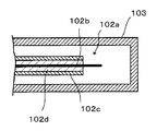
- One end of the coaxial cable 102 is inserted into a plasma generation region in the processing chamber 2, and a portion of the coaxial cable 102 disposed in the processing chamber 2 is covered with a quartz tube 103.
- the quartz tube 103 is for preventing the metal constituting the coaxial cable 102 from being mixed into the semiconductor wafer W as an impurity when performing plasma etching of the semiconductor wafer W in the processing chamber 2. . Therefore, when the plasma monitoring is experimentally performed without processing the semiconductor wafer W, the plasma may be monitored without the quartz tube 103, that is, with the coaxial cable 102 exposed.
- the end portion of the coaxial cable 102 on the side disposed in the processing chamber 2 is a probe 102a, and this portion exposes a core wire (internal conductor) 102b made of a conductor such as aluminum. It is assumed that An outer conductor 102c made of a copper pipe or the like is provided on the outer peripheral portion of the coaxial cable 102, and an insulating material 102d made of resin or the like is provided between the core wire (inner conductor) 102b and the outer conductor 102c. Yes.
- the measurement unit 101 to which the coaxial cable 102 is connected is composed of an oscilloscope having a FFT (Fast Fourier Transform) analysis function, a spectrum analyzer, or the like. And the frequency distribution of the electromagnetic wave which exists in the plasma detected by the probe 102a part of the coaxial cable 102 is detected, and this detected frequency distribution can be displayed.
- FFT Fast Fourier Transform
- the control unit 60 includes a process controller 61 that includes a CPU and controls each unit of the plasma etching apparatus 1, a user interface unit 62, and a storage unit 63.
- the user interface unit 62 includes a keyboard that is used by a process manager to input commands to manage the plasma etching apparatus 1, a display that visualizes and displays the operating status of the plasma etching apparatus 1, and the like.
- the storage unit 63 stores a recipe in which a control program (software) for realizing various processes executed by the plasma etching apparatus 1 under the control of the process controller 61 and processing condition data are stored. Then, if necessary, an arbitrary recipe is called from the storage unit 63 by an instruction from the user interface unit 62 and is executed by the process controller 61, so that the process in the plasma etching apparatus 1 is controlled under the process controller 61. Desired processing is performed.
- recipes such as control programs and processing condition data may be stored in a computer-readable computer storage medium (eg, hard disk, CD, flexible disk, semiconductor memory, etc.), or It is also possible to transmit the data from other devices as needed via a dedicated line and use it online.
- the gate valve 32 When performing plasma etching of the semiconductor wafer W by the plasma etching apparatus 1 having the above configuration, first, after the gate valve 32 is opened, the semiconductor wafer W is carried into the processing chamber 2 from a load lock chamber (not shown), It is placed on the electrostatic chuck 11. The semiconductor wafer W is electrostatically attracted onto the electrostatic chuck 11 by applying a DC voltage from the DC power source 13. Next, the gate valve 32 is closed, and the processing chamber 2 is evacuated to a predetermined degree of vacuum by the exhaust device 35.
- valve 28 is opened, and the flow rate of a predetermined etching gas from the processing gas supply source 30 is adjusted by the mass flow controller 29 while passing through the processing gas supply pipe 27 and the gas inlet 26, so that the upper electrode 21 is hollow. Then, the liquid is uniformly discharged onto the semiconductor wafer W through the discharge holes 23 of the electrode plate 24 as shown by the arrows in FIG.
- the pressure in the processing chamber 2 is maintained at a predetermined pressure. Thereafter, high frequency power having a predetermined frequency is applied to the upper electrode 21 from the first high frequency power supply 40. As a result, a high-frequency electric field is generated between the upper electrode 21 and the susceptor 5 as the lower electrode, and the etching gas is dissociated into plasma.
- high frequency power having a frequency lower than that of the first high frequency power supply 40 is applied from the second high frequency power supply 50 to the susceptor 5 serving as the lower electrode.
- ions in the plasma are drawn to the susceptor 5 side, and the anisotropy of etching is enhanced by ion assist.
- the plasma is monitored by the plasma monitoring device 100.
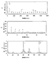
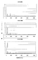
- the frequency distribution (spectrum) of the electromagnetic wave detected by the probe 102 a inserted in the processing chamber 2 is displayed on the measurement unit 101, where the vertical axis represents intensity (intensity) and the horizontal axis represents It is displayed as a graph with frequency.
- Ar 350 sccm, pressure: 13.3 Pa (100 mTorr)
- FIG. 3A due to the high frequency of 60 MHz, in addition to the 60 MHz peak (1), the peaks of the harmonics that are integral multiples of this 60 MHz are from the 2nd to the 19th. 18 appear.
- FIG. 3 (b) due to the high frequency of 2 MHz having a low frequency, in addition to the peak (1) of 2 MHz, the peak of harmonics of an integral multiple of 2 MHz is 3rd to 3rd to 4th. It appears individually.
- FIG. 3 (c) is an enlarged view of a part of FIG. 3 (a).
- a high frequency of 60 MHz is reduced to a low frequency of 2 MHz.
- a plurality of peaks called sidebands obtained by adding and subtracting an integer multiple of.
- a peak of a different frequency whose cause is unknown appears near 80 MHz or 20 MHz between peak (1) (60 MHz) and peak (2) (120 MHz).
- Ar / O 2 500/500 sccm
- pressure 26.6 Pa (200 mTorr)
- 100 shows the plasma monitoring state.
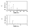
- the peak (1) due to the high frequency of 60 MHz, the peak (1), the peak (2) (120 MHz), the peak (3) (180 MHz), Three harmonic peaks of peak (5) (300 MHz) appear.
- FIG. 4B due to the low frequency of 2 MHz, only the peak of one harmonic of peak (2) (4 MHz) appears in addition to the peak (1) of 2 MHz. ing.
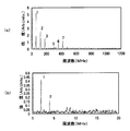
- the peak (1) due to the high frequency of 60 MHz, the peak (1), the peak (2) (120 MHz), the peak (3) (180 MHz), Peaks of five harmonics of peak (5) (300 MHz), peak (6) (360 MHz), and peak (7) (420 MHz) appear.
- FIG. 5B due to the low frequency of 2 MHz, only the peak of one harmonic of peak (2) (4 MHz) appears in addition to the peak (1) of 2 MHz. ing.
- the plasma monitoring results by the plasma monitoring device 100 differ in the position where the peak appears, the height, and the like.
- the monitoring status is shown.
- the upper part of FIG. 6 is a case where the applied power of a high frequency of 2 MHz is 500 W
- the middle part of FIG. 6 is a case where the applied power of a high frequency of 2 MHz is 1000 W
- the lower part of FIG. is there.
- Ar 350 sccm
- pressure 13.3 Pa (100 mTorr)
- the upper part of FIG. 7 is a case where the applied power of a high frequency of 60 MHz is 500 W
- the middle part of FIG. 7 is a case where the applied power of a high frequency of 60 MHz is 1000 W
- the lower part of FIG. is there.
- harmonic peaks appear at 2 MHz, 4 MHz, 6 MHz, and 8 MHz, and when attention is paid to the spectral intensity of 2 MHz, the power value is about 0.2 (Arb.Units.) And the power value is 1000 W. About 0.4 (Arb.Units.) And about 0.6 (Arb.Units.) At a power value of 1500 W, the harmonic intensity increases in proportion to the power value.
- the peak of the harmonic appears at 60 MHz, 120 MHz, and 180 MHz, and the intensity increases as the power value increases.
- FIGS. 3A and 3B In a state where a large number of 60 MHz harmonics and 2 MHz harmonics appear in FIGS. 3A and 3B, and in a state where sidebands and different frequencies of 20 MHz and 80 MHz appear as shown in FIG. It is estimated that the applied high frequency power is not efficiently used and there is a large loss of high frequency power. That is, when FIG. 3A is compared with FIG. 4A, FIG. 3A shows that there are as many as 19 harmonic peaks of 60 MHz and high-frequency power is dispersed, whereas FIG. ) Has only four harmonic peaks, and it can be said that the loss of high-frequency power is extremely small. Further, when FIG. 3B is compared with FIG. 4B, FIG.
- FIG. 3B shows four harmonic peaks at 2 MHz, whereas FIG. 4B shows two harmonic peaks.
- FIG. 4B is about 10 times that of FIG.
- the loss of high-frequency power applied to the lower electrode 5 is large.
- FIG. 3B in a state where a large number of harmonics appear, or in a state where different frequencies or sideband peaks appear, the applied high-frequency power is not efficiently used, Power loss is large.
- the conditions for generating plasma for example, at least one of the supply state of the processing gas, the exhaust state, and the application state of the high-frequency power
- the monitoring state as shown in FIGS. Therefore, it is possible to perform plasma processing with high efficiency and high processing speed.
- plasma monitoring is continuously performed by the plasma monitoring apparatus 100, it is possible to detect the occurrence of any troubles in the apparatus, changes in the plasma generation state due to the consumption of consumable parts, and the like.
- the peak of the high frequency component on the low frequency side is lowered, it is predicted that the etching rate will decrease, so the applied power of the high frequency on the low frequency side is increased.
- the applied power of the high frequency on the low frequency side is increased.
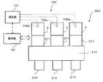
- a plurality of (three in the example of FIG. 8) processing chambers 2 are provided via a load lock chamber 211 for one transfer mechanism 210 that transfers a semiconductor wafer in the atmosphere. Evaluation of machine differences and suppression of machine differences in each processing chamber 2 of the connected plasma processing apparatus 200 can be performed.
- each processing chamber 2 is provided with the probe 102a of the plasma monitoring device 100 described above, and the control unit 60 determines that each processing chamber is based on the monitoring results of the plasma measured by the probe 102a and the measuring unit 101. Control is performed so that the plasma states in the two are the same. Thereby, the difference of the processing state by the machine difference of each processing chamber 2 is suppressed.
- reference numeral 212 denotes a mounting table on which a cassette or a FOUP containing a semiconductor wafer is mounted.
- Specific control when a plurality of processing chambers 2 are provided as described above is performed as follows, for example. That is, a frequency distribution during an actual process in each processing chamber 2 is obtained for each processing chamber 2 and, for example, spectral intensities having a frequency of 60 MHz are compared. Then, by controlling the power of the high frequency power, the pressure, the flow rate of the processing gas, and the like so that the spectrum intensities of 60 MHz coincide with each other, the plasma state in each processing chamber 2 is made the same and the machine difference is reduced.
- the plasma processing apparatus is not limited to the parallel plate type upper and lower high-frequency application type shown in FIG. 1, but can be applied to various plasma processing apparatuses.
- the plasma processing apparatus of the present invention can be used in the field of manufacturing semiconductor devices. Therefore, it has industrial applicability.
Landscapes
- Physics & Mathematics (AREA)
- Engineering & Computer Science (AREA)
- Plasma & Fusion (AREA)
- Chemical & Material Sciences (AREA)
- Analytical Chemistry (AREA)
- Spectroscopy & Molecular Physics (AREA)
- Drying Of Semiconductors (AREA)
- Plasma Technology (AREA)
Abstract
Description
請求項1記載のプラズマ処理装置は、内部に被処理基板が配置される処理チャンバーと、前記処理チャンバー内に所定の処理ガスを供給するガス供給機構と、前記処理チャンバー内から排気する排気機構と、前記処理チャンバー内に前記処理ガスのプラズマを発生させるプラズマ発生機構と、プローブが前記処理チャンバー内に配置される同軸ケーブルと、前記同軸ケーブルと接続され、前記プローブによって検出されたプラズマ中に存在する電磁波の周波数分布を検出する測定部とを備えたプラズマモニタリング装置と、を具備したことを特徴とする。
Claims (5)
- 内部に被処理基板が配置される処理チャンバーと、
前記処理チャンバー内に所定の処理ガスを供給するガス供給機構と、
前記処理チャンバー内から排気する排気機構と、
前記処理チャンバー内に前記処理ガスのプラズマを発生させるプラズマ発生機構と、
プローブが前記処理チャンバー内に配置される同軸ケーブルと、前記同軸ケーブルと接続され、前記プローブによって検出されたプラズマ中に存在する電磁波の周波数分布を検出する測定部とを備えたプラズマモニタリング装置と、
を具備したことを特徴とするプラズマ処理装置。 - 請求項1記載のプラズマ処理装置であって、
前記測定部は、プラズマ中に存在する異周波成分及びサイドバンド成分の少なくとも一方を検出することを特徴とするプラズマ処理装置。 - 請求項1記載のプラズマ処理装置であって、
前記処理チャンバーを複数具備し、前記プラズマモニタリング装置の検出結果に基づいて、複数の前記処理チャンバー内のプラズマの状態が一致するようにプラズマを制御する制御部を有することを特徴とするプラズマ処理装置。 - 請求項3記載のプラズマ処理装置であって、
前記制御部は、前記ガス供給機構、前記排気機構、及び前記プラズマ発生機構の少なくとも一つを制御することを特徴とするプラズマ処理装置。 - 内部に被処理基板が配置される処理チャンバーと、
前記処理チャンバー内に所定の流量の処理ガスを供給するガス供給機構と、
前記処理チャンバー内を所定の真空度に設定する排気機構と、
高周波電源を有し、前記処理チャンバー内に前記処理ガスのプラズマを発生させるプラズマ発生機構と、
前記プラズマにプローブを挿入して、プラズマ中に存在する異周波成分およびサイドバンド成分の少なくとも一方を検出する測定部と、
前記検出結果に基づいて、前記ガス供給機構、前記排気機構および前記プラズマ発生機構の少なくとも一つを制御する制御手段と、
を具備したことを特徴とするプラズマ処理装置。
Priority Applications (4)
| Application Number | Priority Date | Filing Date | Title |
|---|---|---|---|
| US12/920,731 US20110061811A1 (en) | 2008-03-07 | 2009-02-26 | Plasma processing apparatus |
| CN2009800004550A CN101720503B (zh) | 2008-03-07 | 2009-02-26 | 等离子体处理装置 |
| JP2010501866A JPWO2009110366A1 (ja) | 2008-03-07 | 2009-02-26 | プラズマ処理装置 |
| KR1020097026146A KR101089951B1 (ko) | 2008-03-07 | 2009-02-26 | 플라즈마 처리 장치 |
Applications Claiming Priority (2)
| Application Number | Priority Date | Filing Date | Title |
|---|---|---|---|
| JP2008-057883 | 2008-03-07 | ||
| JP2008057883 | 2008-03-07 |
Publications (1)
| Publication Number | Publication Date |
|---|---|
| WO2009110366A1 true WO2009110366A1 (ja) | 2009-09-11 |
Family
ID=41055926
Family Applications (1)
| Application Number | Title | Priority Date | Filing Date |
|---|---|---|---|
| PCT/JP2009/053510 Ceased WO2009110366A1 (ja) | 2008-03-07 | 2009-02-26 | プラズマ処理装置 |
Country Status (5)
| Country | Link |
|---|---|
| US (1) | US20110061811A1 (ja) |
| JP (1) | JPWO2009110366A1 (ja) |
| KR (1) | KR101089951B1 (ja) |
| CN (1) | CN101720503B (ja) |
| WO (1) | WO2009110366A1 (ja) |
Cited By (3)
| Publication number | Priority date | Publication date | Assignee | Title |
|---|---|---|---|---|
| JP2022016547A (ja) * | 2017-04-28 | 2022-01-21 | エーエスエムエル ネザーランズ ビー.ブイ. | 製品ユニットの製造プロセスのシーケンスの最適化 |
| JP2023509794A (ja) * | 2020-01-10 | 2023-03-09 | コメット テクノロジーズ ユーエスエー インコーポレイテッド | プラズマ不均一性検出 |
| JP2023163641A (ja) * | 2022-04-28 | 2023-11-10 | 東京エレクトロン株式会社 | 基板処理方法、コンピュータ記憶媒体及び基板処理装置 |
Families Citing this family (8)
| Publication number | Priority date | Publication date | Assignee | Title |
|---|---|---|---|---|
| WO2013011968A1 (ja) * | 2011-07-16 | 2013-01-24 | イマジニアリング株式会社 | プラズマ生成装置、及び内燃機関 |
| US20130309785A1 (en) * | 2012-05-18 | 2013-11-21 | Applied Materials, Inc. | Rotational absorption spectra for semiconductor manufacturing process monitoring and control |
| GB201705202D0 (en) * | 2017-03-31 | 2017-05-17 | Univ Dublin City | System and method for remote sensing a plasma |
| KR102111206B1 (ko) * | 2017-09-05 | 2020-05-14 | 도쿄엘렉트론가부시키가이샤 | 플라즈마 프로브 장치 및 플라즈마 처리 장치 |
| US11153960B1 (en) * | 2018-06-08 | 2021-10-19 | Innoveering, LLC | Plasma-based electro-optical sensing and methods |
| JP2020202052A (ja) * | 2019-06-07 | 2020-12-17 | 東京エレクトロン株式会社 | プラズマ電界モニタ、プラズマ処理装置、およびプラズマ処理方法 |
| WO2021048995A1 (ja) | 2019-09-13 | 2021-03-18 | 株式会社日立ハイテク | 半導体装置の製造方法及びプラズマ処理装置 |
| JP7598443B2 (ja) | 2022-03-07 | 2024-12-11 | 株式会社日立ハイテク | プラズマ処理方法 |
Citations (2)
| Publication number | Priority date | Publication date | Assignee | Title |
|---|---|---|---|---|
| JP2003017296A (ja) * | 2001-07-05 | 2003-01-17 | Nisshin:Kk | プラズマ密度情報測定方法及びその装置、並びにプラズマ密度情報測定用プローブ、プラズマ密度情報測定用記録媒体、プラズマ処理装置 |
| JP2007294909A (ja) * | 2006-03-29 | 2007-11-08 | Tokyo Electron Ltd | プラズマ処理装置 |
Family Cites Families (2)
| Publication number | Priority date | Publication date | Assignee | Title |
|---|---|---|---|---|
| JP5404984B2 (ja) * | 2003-04-24 | 2014-02-05 | 東京エレクトロン株式会社 | プラズマモニタリング方法、プラズマモニタリング装置及びプラズマ処理装置 |
| US7655110B2 (en) * | 2006-03-29 | 2010-02-02 | Tokyo Electron Limited | Plasma processing apparatus |
-
2009
- 2009-02-26 US US12/920,731 patent/US20110061811A1/en not_active Abandoned
- 2009-02-26 CN CN2009800004550A patent/CN101720503B/zh not_active Expired - Fee Related
- 2009-02-26 KR KR1020097026146A patent/KR101089951B1/ko not_active Expired - Fee Related
- 2009-02-26 WO PCT/JP2009/053510 patent/WO2009110366A1/ja not_active Ceased
- 2009-02-26 JP JP2010501866A patent/JPWO2009110366A1/ja not_active Withdrawn
Patent Citations (2)
| Publication number | Priority date | Publication date | Assignee | Title |
|---|---|---|---|---|
| JP2003017296A (ja) * | 2001-07-05 | 2003-01-17 | Nisshin:Kk | プラズマ密度情報測定方法及びその装置、並びにプラズマ密度情報測定用プローブ、プラズマ密度情報測定用記録媒体、プラズマ処理装置 |
| JP2007294909A (ja) * | 2006-03-29 | 2007-11-08 | Tokyo Electron Ltd | プラズマ処理装置 |
Cited By (7)
| Publication number | Priority date | Publication date | Assignee | Title |
|---|---|---|---|---|
| JP2022016547A (ja) * | 2017-04-28 | 2022-01-21 | エーエスエムエル ネザーランズ ビー.ブイ. | 製品ユニットの製造プロセスのシーケンスの最適化 |
| JP2023052695A (ja) * | 2017-04-28 | 2023-04-11 | エーエスエムエル ネザーランズ ビー.ブイ. | 製品ユニットの製造プロセスのシーケンスの最適化 |
| JP2023509794A (ja) * | 2020-01-10 | 2023-03-09 | コメット テクノロジーズ ユーエスエー インコーポレイテッド | プラズマ不均一性検出 |
| JP7624447B2 (ja) | 2020-01-10 | 2025-01-30 | コメット テクノロジーズ ユーエスエー インコーポレイテッド | プラズマ不均一性検出 |
| JP2025019221A (ja) * | 2020-01-10 | 2025-02-06 | コメット テクノロジーズ ユーエスエー インコーポレイテッド | プラズマ不均一性検出 |
| JP7714102B2 (ja) | 2020-01-10 | 2025-07-28 | コメット テクノロジーズ ユーエスエー インコーポレイテッド | プラズマ不均一性検出 |
| JP2023163641A (ja) * | 2022-04-28 | 2023-11-10 | 東京エレクトロン株式会社 | 基板処理方法、コンピュータ記憶媒体及び基板処理装置 |
Also Published As
| Publication number | Publication date |
|---|---|
| KR20100012875A (ko) | 2010-02-08 |
| CN101720503A (zh) | 2010-06-02 |
| JPWO2009110366A1 (ja) | 2011-07-14 |
| KR101089951B1 (ko) | 2011-12-05 |
| CN101720503B (zh) | 2011-12-21 |
| US20110061811A1 (en) | 2011-03-17 |
Similar Documents
| Publication | Publication Date | Title |
|---|---|---|
| KR101089951B1 (ko) | 플라즈마 처리 장치 | |
| JP5496568B2 (ja) | プラズマ処理装置及びプラズマ処理方法 | |
| JP4884047B2 (ja) | プラズマ処理方法 | |
| JP5373669B2 (ja) | 半導体装置の製造方法 | |
| US9966291B2 (en) | De-chuck control method and plasma processing apparatus | |
| JP5503503B2 (ja) | プラズマ処理装置 | |
| US10553409B2 (en) | Method of cleaning plasma processing apparatus | |
| JPH08264515A (ja) | プラズマ処理装置、処理装置及びエッチング処理装置 | |
| KR20100020927A (ko) | 포커스 링, 플라즈마 처리 장치 및 플라즈마 처리 방법 | |
| JP4828456B2 (ja) | プラズマ処理方法及びプラズマ処理装置 | |
| WO2016056399A1 (ja) | プラズマ処理方法及びプラズマ処理装置 | |
| KR20140092257A (ko) | 플라즈마 처리 방법 및 플라즈마 처리 장치 | |
| JP2017010993A (ja) | プラズマ処理方法 | |
| JP6156850B2 (ja) | プラズマ処理装置及びプラズマ処理装置の部材の交換判断方法 | |
| TWI831956B (zh) | 清潔處理方法及電漿處理裝置 | |
| JP5203986B2 (ja) | フォーカスリングの加熱方法、プラズマエッチング方法、プラズマエッチング装置及びコンピュータ記憶媒体 | |
| JP2011040461A (ja) | バッフル板及びプラズマ処理装置 | |
| JP6219179B2 (ja) | プラズマ処理装置 | |
| JP5302813B2 (ja) | 堆積物対策用カバー及びプラズマ処理装置 | |
| JP2019176032A (ja) | プラズマ処理装置 | |
| JP2008034579A (ja) | プラズマ表面処理方法、石英製部材、プラズマ処理装置およびプラズマ処理方法 | |
| JP5047644B2 (ja) | プラズマエッチング方法、プラズマエッチング装置、制御プログラム及びコンピュータ記憶媒体 | |
| JP2010108997A (ja) | プラズマエッチング方法、プラズマエッチング装置及びコンピュータ記憶媒体 | |
| JP2016086040A (ja) | 半導体製造装置の出力検査方法及び半導体製造装置 |
Legal Events
| Date | Code | Title | Description |
|---|---|---|---|
| WWE | Wipo information: entry into national phase |
Ref document number: 200980000455.0 Country of ref document: CN |
|
| 121 | Ep: the epo has been informed by wipo that ep was designated in this application |
Ref document number: 09718434 Country of ref document: EP Kind code of ref document: A1 |
|
| ENP | Entry into the national phase |
Ref document number: 20097026146 Country of ref document: KR Kind code of ref document: A |
|
| ENP | Entry into the national phase |
Ref document number: 2010501866 Country of ref document: JP Kind code of ref document: A |
|
| NENP | Non-entry into the national phase |
Ref country code: DE |
|
| WWE | Wipo information: entry into national phase |
Ref document number: 12920731 Country of ref document: US |
|
| 122 | Ep: pct application non-entry in european phase |
Ref document number: 09718434 Country of ref document: EP Kind code of ref document: A1 |