WO2009096459A1 - Composition de résine et procédé pour fixer temporairement une pièce à travailler - Google Patents
Composition de résine et procédé pour fixer temporairement une pièce à travailler Download PDFInfo
- Publication number
- WO2009096459A1 WO2009096459A1 PCT/JP2009/051442 JP2009051442W WO2009096459A1 WO 2009096459 A1 WO2009096459 A1 WO 2009096459A1 JP 2009051442 W JP2009051442 W JP 2009051442W WO 2009096459 A1 WO2009096459 A1 WO 2009096459A1
- Authority
- WO
- WIPO (PCT)
- Prior art keywords
- meth
- acrylate
- resin composition
- workpiece
- mass
- Prior art date
Links
Images

Classifications
-
- H—ELECTRICITY
- H02—GENERATION; CONVERSION OR DISTRIBUTION OF ELECTRIC POWER
- H02N—ELECTRIC MACHINES NOT OTHERWISE PROVIDED FOR
- H02N13/00—Clutches or holding devices using electrostatic attraction, e.g. using Johnson-Rahbek effect
-
- C—CHEMISTRY; METALLURGY
- C09—DYES; PAINTS; POLISHES; NATURAL RESINS; ADHESIVES; COMPOSITIONS NOT OTHERWISE PROVIDED FOR; APPLICATIONS OF MATERIALS NOT OTHERWISE PROVIDED FOR
- C09J—ADHESIVES; NON-MECHANICAL ASPECTS OF ADHESIVE PROCESSES IN GENERAL; ADHESIVE PROCESSES NOT PROVIDED FOR ELSEWHERE; USE OF MATERIALS AS ADHESIVES
- C09J4/00—Adhesives based on organic non-macromolecular compounds having at least one polymerisable carbon-to-carbon unsaturated bond ; adhesives, based on monomers of macromolecular compounds of groups C09J183/00 - C09J183/16
-
- C—CHEMISTRY; METALLURGY
- C09—DYES; PAINTS; POLISHES; NATURAL RESINS; ADHESIVES; COMPOSITIONS NOT OTHERWISE PROVIDED FOR; APPLICATIONS OF MATERIALS NOT OTHERWISE PROVIDED FOR
- C09J—ADHESIVES; NON-MECHANICAL ASPECTS OF ADHESIVE PROCESSES IN GENERAL; ADHESIVE PROCESSES NOT PROVIDED FOR ELSEWHERE; USE OF MATERIALS AS ADHESIVES
- C09J9/00—Adhesives characterised by their physical nature or the effects produced, e.g. glue sticks
- C09J9/02—Electrically-conducting adhesives
-
- H—ELECTRICITY
- H01—ELECTRIC ELEMENTS
- H01L—SEMICONDUCTOR DEVICES NOT COVERED BY CLASS H10
- H01L21/00—Processes or apparatus adapted for the manufacture or treatment of semiconductor or solid state devices or of parts thereof
- H01L21/67—Apparatus specially adapted for handling semiconductor or electric solid state devices during manufacture or treatment thereof; Apparatus specially adapted for handling wafers during manufacture or treatment of semiconductor or electric solid state devices or components ; Apparatus not specifically provided for elsewhere
- H01L21/683—Apparatus specially adapted for handling semiconductor or electric solid state devices during manufacture or treatment thereof; Apparatus specially adapted for handling wafers during manufacture or treatment of semiconductor or electric solid state devices or components ; Apparatus not specifically provided for elsewhere for supporting or gripping
- H01L21/6831—Apparatus specially adapted for handling semiconductor or electric solid state devices during manufacture or treatment thereof; Apparatus specially adapted for handling wafers during manufacture or treatment of semiconductor or electric solid state devices or components ; Apparatus not specifically provided for elsewhere for supporting or gripping using electrostatic chucks
Definitions
- the present invention relates to a resin composition for fixing a workpiece to a processing table by electrostatic adsorption.
- the present invention also relates to a method for fixing a workpiece using the resin composition, a surface protection method for the workpiece, and a method for temporarily fixing the workpiece.
- the surface protection sheet protects the circuit surface of the wafer and the non-processed surface of the optical component, and is temporarily fixed to the base material via the surface protection sheet.
- the back surface opposite to the circuit surface is ground by a so-called back surface grinding method.
- the pressure-sensitive adhesive surface protection sheet currently in use has a limit in the ability to follow the irregularities of the circuit of the semiconductor wafer. For this reason, contamination due to the ingress of the grinding liquid between the wafer and the surface protective layer often becomes a problem. Further, when dicing a semiconductor wafer, it is difficult to follow a protrusion of 100 ⁇ m or more typified by a bump with a typical semiconductor surface protection sheet, and there is a problem that contamination and chip jumping occur.
- Conventional surface protective sheets are generally sheets having a pressure-sensitive adhesive layer as a surface protective layer on a polymer film material, and the pressure-sensitive adhesive is designed to have a low elastic modulus so as to follow the irregularities of the circuit surface. .
- the elastic modulus is too low, a large stress is applied to the wafer when the sheet is peeled off from the wafer, leading to breakage of the wafer.
- an energy ray easily peelable protective sheet that cures the pressure sensitive adhesive by irradiating energy rays such as ultraviolet rays before peeling the sheet, and reduces the adhesive force between the wafer and the protective sheet.
- the pressure-sensitive adhesive layer is in an uncured state during grinding, and there is a problem that the wafer is damaged during grinding because it is too soft.
- Patent Document 1 discloses a wafer grinding method in which the energy ray easy-peelable protective sheet as described above is attached to a wafer on which a circuit is formed, and the adhesive layer is cured with energy rays, and then the back surface of the wafer is ground. ing.
- Patent Document 2 discloses a hot-melt type semiconductor surface protective sheet.
- the hot-melt type sheet that melts and exhibits fluidity when heated to 60 to 100 ° C. described in Patent Document 2 can follow the unevenness of the circuit surface and exhibit excellent grindability.
- the present inventor is also a material that has sufficient followability to the unevenness of the circuit surfaces of the wafer and optical components and is sufficient as a support during grinding.
- a composition having rigidity a resin composition having a (meth) acrylic monomer and a resin containing a cyclopentadiene skeleton as components is developed (Patent Document 3).
- electrostatic adsorption is one of the means for fixing a semiconductor wafer to a stage such as an etching apparatus in processes such as etching, CVD (chemical vapor deposition), and PVD (physical vapor deposition). Is used.
- electrostatic adsorption cannot in principle adsorb a workpiece made of an insulator to a stage. For this reason, electrostatic adsorption cannot be used in SOS (silicon on sapphire) and SOI (silicon on insulator), which are expected as next-generation substitutes for silicon wafers.
- SOS silicon on sapphire
- SOI silicon on insulator
- an electrostatic substrate cannot be used because an insulating substrate such as a glass substrate is used.
- Patent Document 4 a method has been proposed in which a conductive film is provided on a suction surface of a workpiece or a conductive film is attached to make a surface to be electrostatically attracted conductive.
- Patent Document 6 a composition containing a conductive component, a binder component (resin), and a curing agent has been proposed as a conductive coating composition for temporarily protecting electronic devices and electronic elements from electrostatic discharge and electromagnetic interference.
- the hot-melt type semiconductor surface protective sheet described in Patent Document 2 has a property of melting whenever the temperature exceeds the melting point, and when an insulating substrate is used, electrostatic adsorption is used. I can't.
- the film is mainly formed by vapor deposition. It was necessary to remove.
- the method of applying the conductive film described in Patent Document 5 has a problem that the film is wrinkled or peeled off during processing. Furthermore, in the case where unevenness such as a circuit exists on the surface to be attached, the film has insufficient followability to the unevenness.
- the composition for conductive coating described in Patent Document 6 must use an organic solvent when removing the coating, and has a problem from the viewpoint of reducing environmental burden.
- Japanese Patent Laid-Open No. 11-026406 Japanese Unexamined Patent Publication No. 2000-038556
- the present invention has been made in view of the above circumstances, and enables electrostatic adsorption even when the work material is insulative, and further follows the unevenness of the surface of the work material, adhesive strength, and after processing. It aims at providing the resin composition which is excellent in removability.
- a resin composition that contains an acrylic compound and a conductive material, and is fixed to a processing table by electrostatic adsorption after being applied and cured on the surface of the processing material. Is done.
- this resin composition a resin composition that enables electrostatic attraction even when the work material is insulative, and has excellent followability to unevenness on the work material surface, adhesive strength, and removability after processing. Things are obtained.
- a method for fixing a workpiece is provided.
- a resin composition having excellent followability to unevenness on the surface of the work material, adhesive strength, and removability after processing is applied and cured on the surface of the work material.
- excellent effects can be obtained in terms of labor saving, energy saving, and work shortening.
- a resin composition containing an acrylic compound and a conductive substance has sufficient followability to surface irregularities such as a circuit surface of the workpiece as compared with a method of attaching a conductive film to the surface of the workpiece. Therefore, the surface can be protected from scratches and contamination.
- the cured body of the resin composition containing the acrylic compound and the conductive material can be easily peeled by contact with hot water of 90 ° C. or less, it is fixed to the processing table by this fixing method and processed.
- an effect of being safe and excellent in workability can be obtained as compared with the method of removing the conductive film by etching or the like.
- a resin composition having excellent followability to unevenness on the surface of the work material, adhesive strength, and removability after processing is applied and cured on the surface of the work material.
- excellent effects can be obtained in terms of labor saving, energy saving, and work shortening.
- a resin composition containing an acrylic compound and a conductive substance has sufficient followability to surface irregularities such as a circuit surface of the workpiece as compared with a method of attaching a conductive film to the surface of the workpiece. Therefore, the surface can be protected from scratches and contamination.
- the cured body of the resin composition containing an acrylic compound and a conductive substance can be easily peeled by contact with hot water of 90 ° C. or less, the cured product is fixed on a processing table and processed.
- membrane by an etching etc. is acquired.
- the environmental load is greatly reduced compared to conventional removal methods using organic solvents. be able to.
- lower limit value to upper limit value means that the value is within the range of the lower limit value and the upper limit value.
- (meth) acrylate means a compound classified as either acrylate or methacrylate.
- Embodiments of the present invention relate to an electrostatic adsorption method and a surface protection method for the workpiece when processing various materials, and to a resin composition suitable for the method. More specifically, in the embodiment of the present invention, when processing a semiconductor wafer, an insulating substrate, or the like, the resin composition is applied and cured on the surface of the workpiece to fix the workpiece by electrostatic adsorption. In addition to presenting a possible method, a method for protecting the surface of a workpiece, which is intended to protect a portion not to be processed from adhesion of foreign matter or scratches, is presented. Moreover, after processing a workpiece, the temporary fixing method of the workpiece which collects a workpiece is also shown by immersing the adhesion part of a resin composition in warm water, and removing the hardening body of a resin composition. Is.
- the resin composition according to the present embodiment is a resin composition for fixing the work material to the work table by electrostatic adsorption after being applied and cured on the surface of the work material such as a semiconductor wafer and an insulating substrate.
- the resin composition according to the present embodiment is a resin composition containing an acrylic compound and a conductive substance.
- the resin composition according to the present embodiment contains an acrylic compound and a conductive substance, even when a workpiece such as a semiconductor wafer or an insulating substrate is insulative, the workpiece is applied to the workpiece table. It enables electrostatic attraction, and is excellent in followability to unevenness on the workpiece surface, adhesive strength, and removability after processing.
- the resin composition according to the present embodiment is not particularly limited, and can include any compound as long as it is a compound generally classified as an acrylic compound.
- polyfunctional (meth) acrylate and monofunctional (meta) ) Acrylate and further preferably includes a photopolymerization initiator.
- the resin composition containing polyfunctional (meth) acrylate and monofunctional (meth) acrylate as an acrylic compound and further containing a photopolymerization initiator has photocurability and is cured by ultraviolet light or visible light. Is done.
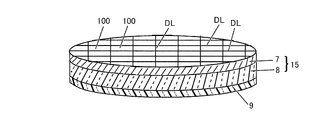
- FIGS. 1 to 3 are process diagrams for explaining a method of fixing a workpiece according to an embodiment of the present invention.
- the work material 15 is fixed to the work table 10 by electrostatic adsorption (FIG. 2), and the work material 15 is immersed in warm water of 90 ° C. or less after being processed.
- the workpiece 15 can be temporarily fixed and processed on the processing table 10 of the processing apparatus.
- the resin composition 9 containing an acrylic compound and a conductive material is used for the surface of the workpiece 15 such as a circuit surface as compared with the method of attaching a conductive film to the surface of the workpiece 15.
- the surface can be protected from scratches and contamination because of its sufficient ability to follow the unevenness.
- the cured body of the resin composition 9 containing the acrylic compound and the conductive material can be easily peeled by contacting with warm water of 90 ° C. or less.
- warm water of 90 ° C. or less.
- an effect of being safe and excellent in workability can be obtained as compared with a method of removing the conductive film by etching or the like.
- cured material of the resin composition 9 can be easily peeled by making it contact with warm water, an environmental load can be reduced significantly compared with the conventional removal method which uses an organic solvent.
- the (A) polyfunctional (meth) acrylate used in the present embodiment is not particularly limited as long as it is a compound having a plurality of (meth) acryloyl groups in the molecule, and any compound can be used.
- a polyfunctional (meth) acrylate oligomer / polymer / monomer having two or more (meth) acryloyl groups can be used.
- the polyfunctional (meth) acrylate oligomer / polymer is not particularly limited as long as it is an oligomer / polymer having a plurality of (meth) acryloyl groups in the molecule, and any compound can be used.
- 2-polybutadiene-terminated urethane (meth) acrylate for example, “TE-2000”, “TEA-1000” manufactured by Nippon Soda Co., Ltd.), hydrogenated product thereof (for example, “TEAI-1000” manufactured by Nippon Soda Co., Ltd.), 1 , 4-polybutadiene-terminated urethane (meth) acrylate (for example, “BAC-45” manufactured by Osaka Organic Chemical Co., Ltd.), polyisoprene-terminated (meth) acrylate, polyester-based urethane (meth) acrylate (for example, “manufactured by Nippon Gosei Co., Ltd.
- UV-3000B Polyether urethane (meth) acrylate, polyester (medium ) Acrylate, bisphenol A type epoxy (meth) acrylate (for example, “Biscoat # 540” manufactured by Osaka Organic Chemical Co., Ltd., “Biscoat VR-77” manufactured by Showa High Polymer Co., Ltd.) and the like.
- a photopolymerization initiator is further added to the resin composition containing these compounds, it exhibits excellent photocurability with respect to ultraviolet light or visible light.
- the bifunctional (meth) acrylate monomer is not particularly limited as long as it is a monomer having two (meth) acryloyl groups in the molecule, and any compound can be used.
- the oligomer / polymer which has several (meth) acryloyl group in a molecule
- an oligomer / polymer having a plurality of (meth) acryloyl groups in the molecule 1,2-polybutadiene-terminated urethane (meth) acrylate, hydrogenated product thereof, and polyester urethane (meth) acrylate 1 type or 2 types or more are preferable and 1, 2- polybutadiene terminal urethane (meth) acrylate is more preferable.
- the bifunctional (meth) acrylate monomer dicyclopentanyl di (meth) acrylate and / or 1,6-hexanediol di (meth) acrylate is preferable, and dicyclopentanyl di (meth) acrylate is more preferable.
- the content ratio of the oligomer / polymer having a plurality of (meth) acryloyl groups in the molecule and the bifunctional (meth) acrylate monomer is preferably 30 to 85:70 to 15, more preferably 45 to 70:55 to 30 by mass ratio. preferable.
- the (A) polyfunctional (meth) acrylate used in the present embodiment is not particularly intended to exclude hydrophilic ones, but is preferably hydrophobic ones.
- hydrophobicity it is possible to suppress a phenomenon that tends to occur in the case of water-solubility and causes a positional shift due to swelling of the cured body of the resin composition during processing, resulting in poor processing accuracy.
- hydrophobic means (meth) acrylate having no hydroxyl group. Even if it is hydrophilic, it can be used as long as the cured product of the resin composition is not greatly swollen or partially dissolved by water.
- the addition amount of (A) polyfunctional (meth) acrylate is preferably 5 to 50 parts by mass in 100 parts by mass of (A) polyfunctional (meth) acrylate and (B) monofunctional (meth) acrylate described later. Particularly preferred is 30 to 40 parts by mass.
- the addition amount of polyfunctional (meth) acrylate is 5 mass parts or more or 30 masses in 100 mass parts of total mass of (A) polyfunctional (meth) acrylate and (B) monofunctional (meth) acrylate mentioned later.
- the peelability is lowered and the cured product of the resin composition does not become a film, and if it is 50 parts by mass or less or 40 parts by mass or less, the curing shrinkage increases and the initial adhesion The possibility that the performance is lowered can be reduced.
- the monofunctional (meth) acrylate monomer of the component (B) is not particularly limited as long as it is a compound having one (meth) acryloyl group in the molecule, and any compound can be used.
- 2- (1,2-cyclohexanedicarboximido) ethyl (meth) acrylate, phenol ethylene oxide 2 mol modified (meth) acrylate, dicyclopentenyloxyethyl (meth) acrylate One or more of the group consisting of benzyl (meth) acrylate and isobornyl (meth) acrylate are preferred, phenol ethylene oxide 2 mol modified (meth) acrylate and / or dicyclopentenyloxyethyl (meth) acrylate, It is more preferable to contain 2- (1,2-cyclohexanedicarboximido) ethyl (meth) acrylate, and phenol ethylene oxide 2 molar modified (meth) acrylate and 2- (1,2-cyclohexanedicarboxyimid) ) And ethyl (meth) acrylate, it is most preferable to contain.
- the content ratio of 2- (1,2-cyclohexanedicarboximido) ethyl (meth) acrylate and phenol ethylene oxide 2-mol modified (meth) acrylate and / or dicyclopentenyloxyethyl (meth) acrylate is expressed by mass ratio. 35 to 80:65 to 20 is preferable, and 45 to 70:55 to 30 is more preferable in that the cured product of the resin composition exhibits good peelability.
- the monofunctional (meth) acrylate is not particularly intended to exclude hydrophilic ones, but is preferably a hydrophobic one as in the case of (A) polyfunctional (meth) acrylates.
- hydrophobicity it is possible to suppress a phenomenon that tends to occur in the case of water-solubility and causes a positional shift due to swelling of the cured body of the resin composition during processing, resulting in poor processing accuracy.
- hydrophobic means (meth) acrylate having no hydroxyl group. Even if it is hydrophilic, it can be used as long as the cured product of the resin composition hardly swells or partially dissolves with water.
- the addition amount of the (B) monofunctional (meth) acrylate is preferably 50 to 95 parts by mass in the total mass of 100 parts by mass of the (A) polyfunctional (meth) acrylate and the (B) monofunctional (meth) acrylate.
- the amount is preferably 60 to 70 parts by mass.
- the addition amount of monofunctional (meth) acrylate is 50 parts by mass or more or 60 parts by mass or more in the total mass of 100 parts by mass of (A) polyfunctional (meth) acrylate and (B) monofunctional (meth) acrylate.
- the possibility that the initial adhesiveness is lowered can be reduced, and if it is 95 parts by mass or less or 70 parts by mass or less, the peelability is hardly lowered, and a cured product of the resin composition is easily obtained in a film form.
- the resin composition of the present embodiment further includes (meth) acryloyloxyethyl acid phosphate, Dibutyl 2- (meth) acryloyloxyethyl acid phosphate, dioctyl 2- (meth) acryloyloxyethyl phosphate, diphenyl 2- (meth) acryloyloxyethyl phosphate, (meth) acryloyloxyethyl polyethylene glycol acid phosphate, etc.
- the phosphate ester which has a vinyl group or a (meth) acryloyl group, the adhesiveness to a metal surface can further be improved.
- the conductive material (C) used in the present embodiment is not particularly limited as long as it is a conductive material.
- a conductive material for example, metal particles, metal-coated resins, conductive materials can be used.
- conductive metal oxide, carbon black, and graphite are preferable.
- one or more of the group consisting of silver, aluminum, and indium tin oxide is preferable because of its great effect.
- metal particles examples include gold, silver (Ag), copper, aluminum (Al), nickel and the like from the viewpoint of conductivity and stability.
- Examples of the conductive metal oxide include zinc oxide, tin oxide, indium oxide, indium tin oxide (ITO), and antimony tin oxide (ATO) from the viewpoint of conductivity and stability.
- the shape of the conductive material is not particularly limited, and any shape such as a plate shape, a rod shape, or a scale shape can be used in addition to a spherical shape.
- conductive polymers such as polyacetylene, polypyrrole, and polythiophene, ionic liquids, antistatic agents, and the like can be used as the conductive substance. These conductive substances may be used alone or in combination of two or more.
- the conductive material one or more of the group consisting of silver, aluminum, and indium tin oxide is preferable because of its great effect.
- the particle diameter of the metal particles is preferably 100 nm to 300 ⁇ m, more preferably 1 ⁇ m to 50 ⁇ m, in terms of the average particle diameter of the particles. If the average particle diameter of the metal particles is 100 nm or more, handling properties can be ensured, and if it is 300 ⁇ m or less, the uniformity of the film thickness of the resin layer due to the granular material described later can be ensured.
- the average particle size was measured with a laser diffraction particle size distribution analyzer (“SALD-2200” manufactured by Shimadzu Corporation).
- the addition amount of the (C) conductive substance is preferably 10 to 500 parts by mass with respect to 100 parts by mass of the total mass of (A) polyfunctional (meth) acrylate and (B) monofunctional (meth) acrylate, Particularly preferred is 50 to 250 parts by mass.
- the added amount is 10 parts by mass or more or 50 parts by mass or more, the conductivity of the resin composition is improved, and the cured product of the resin composition can be electrostatically adsorbed.
- this addition amount is 500 parts by mass or less or 250 parts by mass or less, the followability of the resin composition to the unevenness of the workpiece surface, handling properties, adhesive strength, photocurability, and removability after processing. Deterioration can be suppressed.
- the photopolymerization initiator (D) used in the present embodiment is blended to accelerate photocuring of the resin composition by sensitizing with actinic rays of visible light or ultraviolet rays, and various known photopolymerizations. Initiators can be used.
- the photopolymerization initiator include benzophenone and derivatives thereof, benzyl and derivatives thereof, anthraquinone and derivatives thereof, benzoin, benzoin methyl ether, benzoin ethyl ether, benzoin propyl ether, benzoin isobutyl ether, and benzyldimethyl.
- Benzoin derivatives such as ketal, acetophenone derivatives such as diethoxyacetophenone, 4-t-butyltrichloroacetophenone, 2-dimethylaminoethylbenzoate, p-dimethylaminoethylbenzoate, diphenyldisulfide, thioxanthone and its derivatives, camphorquinone, 7,7 -Dimethyl-2,3-dioxobicyclo [2.2.1] heptane-1-carboxylic acid, 7,7-dimethyl-2,3-dioxobicyclo [2.2.1] Heptane-1-carboxy-2-bromoethyl ester, 7,7-dimethyl-2,3-dioxobicyclo [2.2.1] heptane-1-carboxy-2-methyl ester, 7,7-dimethyl-2 , 3-dioxobicyclo [2.2.1] heptane-1-carboxylic acid chloride and
- photopolymerization initiators When these photopolymerization initiators are further added to a resin composition containing an acrylic compound such as (A) a polyfunctional (meth) acrylate and (B) a monofunctional (meth) acrylate, it is excellent for ultraviolet light or visible light. It is for exhibiting photocurability.
- acrylic compound such as (A) a polyfunctional (meth) acrylate and (B) a monofunctional (meth) acrylate
- A a polyfunctional (meth) acrylate
- B a monofunctional (meth) acrylate
- these photoinitiators can be used 1 type or in combination of 2 or more types.
- the addition amount of the photopolymerization initiator is preferably 0.1 to 20 parts by mass relative to 100 parts by mass of the total mass of (A) polyfunctional (meth) acrylate and (B) monofunctional (meth) acrylate. More preferably, it is 3 to 10 parts by mass. If this addition amount is 0.1 parts by mass or more, the effect of curing acceleration can be surely obtained, and by adding 3 parts by mass or more, it becomes possible to cure without depending on the amount of light irradiation. It is more preferable in that it does not cause misalignment and the like and the peelability is improved. On the other hand, if this addition amount is 20 parts by mass or less or 10 parts by mass or less, a sufficient curing rate can be achieved.
- the resin composition of this embodiment can use a small amount of a polymerization inhibitor for improving the storage stability.
- the polymerization inhibitor is not particularly limited as long as it is a substance that suppresses polymerization of acrylic compounds such as (A) polyfunctional (meth) acrylate and (B) monofunctional (meth) acrylate, and any substance may be used.
- hydroquinone for example, methyl hydroquinone, hydroquinone, 2,2-methylene-bis (4-methyl-6-tertiary butylphenol), catechol, hydroquinone monomethyl ether, monotertiary butyl hydroquinone, 2,5-ditertiary butyl hydroquinone P-benzoquinone, 2,5-diphenyl-p-benzoquinone, 2,5-ditertiarybutyl-p-benzoquinone, picric acid, citric acid, phenothiazine, tertiary butylcatechol, 2-butyl-4-hydroxyanisole and 2 , 6-Jitter Shari Butyl -p- cresol, and the like.
- the amount of the polymerization inhibitor used is preferably 0.001 to 3 parts by mass with respect to 100 parts by mass of the total mass of (A) polyfunctional (meth) acrylate and (B) monofunctional (meth) acrylate. More preferred is 01 to 2 parts by mass.
- the amount of the polymerization inhibitor used is 0.001 parts by mass or more or 0.01 parts by mass or more with respect to 100 parts by mass of the total mass of (A) polyfunctional (meth) acrylate and (B) monofunctional (meth) acrylate. If it is present, the storage stability is sufficient, and if the amount used is 3 parts by mass or less or 2 parts by mass or less, reliable adhesiveness is obtained, and the possibility of being uncured is also reduced.
- the particulate material that does not dissolve in (A) and (B) may be either organic particles or inorganic particles that are generally used as the material.
- examples of the organic particles include polyethylene particles, polypropylene particles, crosslinked polymethyl methacrylate particles, and crosslinked polystyrene particles, and examples of inorganic particles include ceramic particles such as glass, silica, alumina, and titanium.
- the granular material not dissolved in (A) and (B) is preferably spherical and has a constant particle size from the viewpoint of improving the grinding thickness accuracy, that is, controlling the thickness of the resin layer.
- the organic particles include methyl methacrylate monomers, crosslinked polymethyl methacrylate particles obtained as monodisperse particles by a known emulsion polymerization method of a styrene monomer and a crosslinkable monomer, and crosslinked polystyrene particles.
- examples of inorganic particles include spherical silica.
- These particles are preferable because the deformation of the particles is small and the film thickness of the resin layer is uniform due to the variation in particle diameter, and among them, from the viewpoint of storage stability such as sedimentation of the particles and reactivity of the resin composition, among others.
- Cross-linked polymethyl methacrylate particles and cross-linked polystyrene particles are even more preferable.
- the film thickness of the cured product of the resin composition can be appropriately selected by those skilled in the art according to the type, shape, size, etc. of the member, but the particle diameter of the particulate material that does not dissolve in (A) and (B)
- the average particle diameter is preferably 1 to 300 ⁇ m, more preferably 10 to 200 ⁇ m. If the film thickness of the cured resin composition is 1 ⁇ m or more, releasability can be secured, and if it is 300 ⁇ m or less, the processing accuracy does not decrease.
- the average particle diameter means an average particle diameter that can be measured with a laser diffraction particle size distribution analyzer (for example, “SALD-2200” manufactured by Shimadzu Corporation).
- the amount of the particulate material not dissolved in (A) and (B) is preferably 0.1 to 20 parts by mass, particularly 0.1 to 10 parts per 100 parts by mass of the total amount of (A) and (B). Part by mass is preferred. If the added amount of the particulate material not dissolved in (A) and (B) is 0.1 parts by mass or more with respect to 100 parts by mass of the total amount of (A) and (B), the film thickness of the resin layer is almost the same. If it is constant and is 20 parts by mass or less, there is no possibility that the initial adhesiveness is lowered.
- the resin composition according to the present embodiment may contain a polar organic solvent in addition to the various components described above.
- a polar organic solvent is not particularly limited as long as it is a solvent generally classified as a polar solvent, and examples thereof include alcohols, ketones and esters. Of these, alcohol is preferably selected according to the results of investigation by the inventors (Data not shown). Examples of the alcohol include methanol, ethanol, n-propanol, isopropanol, n-butanol, isobutanol, sec-butanol, tert-butanol, n-amyl alcohol, isoamyl alcohol, 2-ethylbutyl alcohol and the like.
- methanol, ethanol, n-propanol, isopropanol, n-butanol, isobutanol, sec-butanol, and tert-butanol having a boiling point of 120 ° C. or less are preferred, among which methanol, More preferred are ethanol, isopropanol, and n-butanol.
- the boiling point is preferably 50 ° C. or higher and 200 ° C. or lower.
- a polar organic solvent having a boiling point within this range it is preferable because a phenomenon in which the cured composition comes into contact with warm water and the adhesive strength decreases can be more reliably exhibited.
- the addition amount of the polar organic solvent is preferably 0.5 to 10 parts by mass with respect to 100 parts by mass as the total mass of (A) polyfunctional (meth) acrylate and (B) monofunctional (meth) acrylate. Peelability is ensured if the amount of the polar organic solvent added is 0.5 parts by mass or more with respect to 100 parts by mass of the total mass of (A) polyfunctional (meth) acrylate and (B) monofunctional (meth) acrylate. If the added amount is 10 parts by mass or less, the risk of lowering the initial adhesiveness is reduced, and the cured product of the resin composition is easily peeled into a film.
- the acrylic resin composition used in the present embodiment may contain various elastomers such as commonly used acrylic rubber, urethane rubber, acrylonitrile-butadiene-styrene rubber, and the like within a range that does not impair the purpose of the present embodiment. Further, additives such as a solvent, an extender, a reinforcing material, a plasticizer, a thickener, a dye, a pigment, a flame retardant, a silane coupling agent, and a surfactant may be included.
- additives such as a solvent, an extender, a reinforcing material, a plasticizer, a thickener, a dye, a pigment, a flame retardant, a silane coupling agent, and a surfactant may be included.
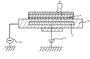
- ⁇ Method of fixing workpiece> 1 to 3 are process diagrams for explaining a method of fixing a workpiece according to an embodiment of the present invention.
- the method of fixing the workpiece 15 according to this embodiment includes a step of applying and curing a resin composition 9 containing an acrylic compound and a conductive substance on the surface of the workpiece 15 (FIG. 1), and electrostatic adsorption.
- a method of fixing the workpiece 15 including the step of fixing the workpiece 15 to the processing table 10 (FIG. 2).
- the resin composition 9 containing an acrylic compound and a conductive substance on the surface of the workpiece the resin composition is applied by a gap coater, spin coater, brush, spray, or the like. After that, coating and curing are performed such that the resin composition is cured by irradiating ultraviolet rays with an ultraviolet irradiation device.
- the processing material 15 coated and cured with the resin composition 9 is placed on the processing table 10, and then the internal electrode is connected by the power source 13.
- the fixing is performed by applying a voltage to 11 and fixing the workpiece 15 to the processing table 10 by electrostatic adsorption.
- the AC power supply 14 of FIG. 2 is provided to remove the remaining electrostatic attraction force.
- the process of processing a workpiece may be further included after the process of fixing the workpiece to the processing table by the electrostatic adsorption.
- processing such as etching, CVD, and PVD is performed.
- the fixing method of the workpiece 15 further includes a step (FIG. 3) of removing the cured product of the resin composition from the workpiece by immersing the workpiece 15 in warm water of 90 ° C. or lower after processing. Also good.
- the fixing method of the workpiece 15 can also be regarded as a surface protection method of the workpiece 15 or a primary fixing method of the workpiece 15 depending on the focus. In any case, this method enables electrostatic adsorption even on an insulator such as the semiconductor wafer 7 and the glass substrate 8 and enables processing such as etching.
- the resin composition 9 having excellent followability to the unevenness on the surface of the workpiece 15, adhesive strength, and removability after processing is applied and cured on the surface of the workpiece 15, CVD or Compared with the method of forming a conductive film on the surface of the workpiece 15 by PVD, excellent effects can be obtained in terms of labor saving, energy saving, and work shortening.
- the resin composition 9 containing an acrylic compound and a conductive material is used for the surface of the workpiece 15 such as a circuit surface as compared with the method of attaching a conductive film to the surface of the workpiece 15. The surface can be protected from scratches and contamination because of its sufficient ability to follow the unevenness.
- the cured body of the resin composition 9 containing the acrylic compound and the conductive material can be easily peeled by contacting with warm water of 90 ° C. or less.
- warm water of 90 ° C. or less.
- an effect of being safe and excellent in workability can be obtained as compared with a method of removing the conductive film by etching or the like.
- cured material of the resin composition 9 can be easily peeled by making it contact with warm water, an environmental load can be reduced significantly compared with the conventional removal method which uses an organic solvent.
- the workpiece 15 is not limited to the semiconductor wafer 7 or the glass substrate 8, and a workpiece made of any material can be used.
- a workpiece made of any material can be used.
- quartz or ceramics can be used. It may be an insulator such as plastic, a semiconductor, or a conductor. This is because even with these workpieces, similar effects can be obtained according to the above method.
- a process of applying and curing a resin composition 9 containing an acrylic compound and a conductive substance on the surface of the workpiece 15, and processing by electrostatic adsorption A step of fixing the material 15 to the work table 10 and a step of removing the cured body of the resin composition 9 from the work material 15 by immersing the work material 15 in hot water of 90 ° C. or less after the work material 15 is processed. It is also a method for protecting the surface of the material 15. That is, according to this method for protecting the surface of the workpiece 15, the resin composition 9 is applied to the surface of the workpiece 15 that is not processed and cured to prevent the surface from being stained or damaged during processing. be able to.
- the above-described method can be performed by applying and curing a resin composition 9 containing an acrylic compound and a conductive material on the surface of the workpiece 15 and electrostatic adsorption.
- This is also a temporary fixing method of the workpiece 15. That is, according to the temporary fixing method of the work material 15, when the cured body of the resin composition 9 is removed, it can be recovered from the work material 15 in a film state, so that the workability is excellent. can get.
- the method of contacting the cured body of the resin composition 9 with water is recommended because the method of immersing the workpiece 15 and the bonded body of the cured body of the resin composition 9 together in water is simple.
- the workpiece 15 fixing method of the above embodiment is regarded as a surface protection method of the workpiece 15 or a temporary fixing method of the workpiece 15, the workpiece 15 is essentially the same. Since there is no change in the fixing method, the action and effect described in detail in the description of the fixing method of the workpiece 15 are naturally applied to the surface protection method of the workpiece 15 as well. It goes without saying that the same applies to the 15 temporary fixing methods.
- a resin composition that contains an acrylic compound and a conductive material, and is fixed to a processing table by electrostatic adsorption after being applied and cured on the surface of the processing material. Is done.
- the said resin composition contains polyfunctional (meth) acrylate and monofunctional (meth) acrylate as said acrylic compound, and also contains a photoinitiator.
- both the polyfunctional (meth) acrylate and the monofunctional (meth) acrylate are hydrophobic.
- the polyfunctional (meth) acrylate is added to 100 parts by mass of the polyfunctional (meth) acrylate and the monofunctional (meth) acrylate, and the monofunctional It is preferable to contain 50 to 95 parts by weight of (meth) acrylate, 10 to 500 parts by weight of the conductive substance, and 0.1 to 20 parts by weight of the photopolymerization initiator.
- the conductive substance is preferably at least one selected from the group consisting of metals, metal-coated resins, conductive metal oxides, carbon black, and graphite.
- the resin composition preferably contains a polymerization inhibitor.
- the resin composition preferably contains a particulate material that does not dissolve in (A) and (B).
- a step of applying and curing a resin composition containing an acrylic compound and a conductive substance on the surface of the workpiece, a step of fixing the workpiece to the processing table by electrostatic adsorption, A method for fixing a workpiece is provided.
- the said resin composition contains polyfunctional (meth) acrylate and monofunctional (meth) acrylate as said acrylic compound, and also contains a photoinitiator.
- both the polyfunctional (meth) acrylate and the monofunctional (meth) acrylate are hydrophobic.
- the resin composition contains 5 to 50 polyfunctional (meth) acrylates with respect to a total amount of 100 parts by mass of the polyfunctional (meth) acrylate and the monofunctional (meth) acrylate. It is preferable to contain 50 parts by mass of the monofunctional (meth) acrylate, 10 to 500 parts by mass of the conductive substance, and 0.1 to 20 parts by mass of the photopolymerization initiator.
- the conductive substance is preferably at least one selected from the group consisting of metals, metal-coated resins, conductive metal oxides, carbon black, and graphite.
- the resin composition preferably contains a polymerization inhibitor.
- the resin composition preferably contains a particulate material that does not dissolve in (A) and (B).
- a step of applying and curing a resin composition containing an acrylic compound and a conductive substance on the surface of the workpiece a step of fixing the workpiece to the processing table by electrostatic adsorption, And a step of immersing the workpiece in hot water of 90 ° C. or less after processing to remove the cured body of the resin composition from the workpiece.
- the said resin composition contains polyfunctional (meth) acrylate and monofunctional (meth) acrylate as said acrylic compound, and also contains a photoinitiator.
- both the polyfunctional (meth) acrylate and the monofunctional (meth) acrylate are hydrophobic.
- the resin composition contains 5 to 50 polyfunctional (meth) acrylates with respect to a total amount of 100 parts by mass of the polyfunctional (meth) acrylate and the monofunctional (meth) acrylate. It is preferable to contain 50 parts by mass of the monofunctional (meth) acrylate, 10 to 500 parts by mass of the conductive substance, and 0.1 to 20 parts by mass of the photopolymerization initiator.
- the conductive substance is preferably at least one selected from the group consisting of metals, metal-coated resins, conductive metal oxides, carbon black, and graphite.
- the resin composition preferably contains a polymerization inhibitor.
- the resin composition preferably contains a particulate material that does not dissolve in (A) and (B).
- a step of applying and curing a resin composition containing an acrylic compound and a conductive substance on the surface of the workpiece a step of fixing the workpiece to the processing table by electrostatic adsorption, And a step of removing the cured product of the resin composition from the workpiece by immersing the workpiece in warm water of 90 ° C. or lower after processing.
- the said resin composition contains polyfunctional (meth) acrylate and monofunctional (meth) acrylate as said acrylic compound, and also contains a photoinitiator.
- both the polyfunctional (meth) acrylate and the monofunctional (meth) acrylate are hydrophobic.
- the resin composition contains 5 to 50 polyfunctional (meth) acrylates with respect to a total amount of 100 parts by mass of the polyfunctional (meth) acrylate and the monofunctional (meth) acrylate. It is preferable to contain 50 parts by mass of the monofunctional (meth) acrylate, 10 to 500 parts by mass of the conductive substance, and 0.1 to 20 parts by mass of the photopolymerization initiator.
- the conductive substance is preferably at least one selected from the group consisting of metals, metal-coated resins, conductive metal oxides, carbon black, and graphite.
- the resin composition preferably contains a polymerization inhibitor.
- the resin composition preferably contains a particulate material that does not dissolve in (A) and (B).
- the workpiece is insulated. Even in the case of the adhesive, electrostatic adsorption can be achieved, and furthermore, the followability of the resin composition to the unevenness of the surface of the workpiece, the adhesive strength, and the removability after the processing can be realized in a balanced manner.
- Example 1 As polyfunctional (meth) acrylate, “TE-2000” (1,2-polybutadiene-terminated urethane methacrylate, hereinafter abbreviated as “TE-2000”) manufactured by Nippon Soda Co., Ltd., dicyclopentanyl di 15 parts by mass of acrylate (manufactured by Nippon Kayaku Co., Ltd., “KAYARAD R-684”, hereinafter abbreviated as “R-684”), (B) 2- (1,2-cyclohexanedicarboxy as monofunctional (meth) acrylate Imido) ethyl acrylate (Toa Gosei Co., Ltd., “Aronix M-140”, hereinafter abbreviated as “M-140”), 40 parts by mass, phenol ethylene oxide 2 mol modified acrylate (Toa Gosei Co., Ltd., “Aronix M-101A”) Hereinafter, abbreviated as “M-101A”.) 100 parts
- Example 1 Using the acrylic resin composition obtained in Example 1, the tensile shear adhesive strength was measured, the peel test, the possibility of electrostatic adsorption, and the surface protection were evaluated by the following evaluation methods.
- Tensile shear bond strength It measured according to JIS K 6850. Specifically, heat-resistant Pyrex (registered trademark) glass (25 mm ⁇ 25 mm ⁇ 2.0 mm) was used as the adherend, and the bonded portion was 8 mm in diameter. (Registered Trademark) glass was bonded and cured by a fusion device manufactured by Fusion Corporation using an electrodeless discharge lamp under the condition of an integrated light amount of 2000 mJ / cm 2 at a wavelength of 365 nm to prepare a tensile shear bond strength test piece. The prepared test piece was measured for tensile shear bond strength at a tensile rate of 10 mm / min in an environment of a temperature of 23 ° C. and a humidity of 50% using a universal testing machine.
- Peel test An acrylic resin composition is applied to the heat-resistant Pyrex (registered trademark) glass, and the acrylic resin composition is applied under a condition of an integrated light quantity of 2000 mJ / cm 2 with a wavelength of 365 nm using a curing device manufactured by Fusion Corporation using an electrodeless discharge lamp. Curing was performed to prepare a peel test specimen. The obtained specimen was immersed in warm water (80 ° C.), the time for peeling from the heat-resistant Pyrex (registered trademark) glass was measured, and the peeled state was also observed.
- the resin composition was applied on a 100 mm square soda glass so as to have a thickness of 50 ⁇ m, and was cured with a fusion apparatus using an electrodeless discharge lamp under the conditions of a wavelength of 365 nm and an integrated light quantity of 2000 mJ / cm 2 .
- the resin composition was cured.
- the cured product of the resin composition was placed on the adsorption table so that it was on the electrode side, and the possibility of electrostatic adsorption was evaluated.
- the case where the substrate was adsorbed without moving or floating was marked with ⁇ , and the case where the substrate was moved without being adsorbed was marked with x.
- the resin composition was applied to a 100 mm square blue plate glass with a thickness of 50 ⁇ m.
- the resin composition was cured under the conditions of a wavelength of 365 nm and an integrated light quantity of 2000 mJ / cm 2 using a fusion device manufactured by Fusion Corporation using an electrodeless discharge lamp, to prepare a protective film.
- the test was performed in an environment with a temperature of 23 ° C. and a humidity of 50%. Thereafter, dicing was performed under the conditions of a rotational speed of 30000 rpm, a feed rate of 20 mm / sec, and a chip size of 10 mm square, and it was observed whether the protective film was retained after dicing. Specifically, out of 100 chips after dicing, the number of chips from which the protective film was peeled was measured and evaluated.
- Table 1 shows the above evaluation results.
- Example 2 An acrylic resin composition was prepared in the same manner as in Example 1 except that the raw materials of the type shown in Table 1 were used in the composition shown in Table 1. The obtained acrylic resin composition was evaluated in the same manner as in Example 1. The results are shown in Table 1.
- the abbreviation QM means dicyclopentenyloxyethyl methacrylate (Rohm & Haas, “QM-657”).
- the abbreviation TEAI-1000 means a hydrogenated 1,2-polybutadiene-terminated urethane (meth) acrylate (“TEAI-1000” manufactured by Nippon Soda Co., Ltd.).
- the abbreviation 1.6HX-A means 1,6-hexanediol diacrylate (“Light Acrylate 1.6HX-A” manufactured by Kyoeisha Chemical Co., Ltd.).
- the abbreviation BZ in Table 1 means benzyl methacrylate (“Light Ester BZ” manufactured by Kyoeisha Chemical Co., Ltd.).
- the abbreviation IBX means isobornyl methacrylate (“Light Ester IB-X” manufactured by Kyoeisha Chemical Co., Ltd.).
- the abbreviation Ag means silver (spherical, average particle size 10 ⁇ m).
- the abbreviation Al means aluminum (spherical, average particle size 20 ⁇ m).
- Comparative Examples 3 to 5 since the conductive material was not blended, the workpiece could not be fixed by electrostatic adsorption. Furthermore, in Comparative Example 3, since (D) a photopolymerization initiator was not blended, it was not cured even after light irradiation. Moreover, in Comparative Example 4, since the blending amount of (A) polyfunctional (meth) acrylate was small, the cured product of the resin composition did not peel into a film, and adhesive residue was observed on the surface of the glass substrate. In Comparative Example 5, since the blending amount of (A) polyfunctional (meth) acrylate was large, strain due to curing shrinkage was large, cracks were observed on the surface of the cured product, and peeling was not possible.
- Examples 1 to 6 since the conductive material was blended in the acrylic resin composition, the workpiece could be fixed by electrostatic adsorption in any case.
- the resin composition after photopolymerization The adhesive strength of the product was sufficient, and the peeled state of the cured product of the resin composition from the glass substrate after processing the workpiece was also good. Furthermore, the surface of the glass substrate after processing the workpiece was also well protected.
- the present invention can be applied to an insulator such as a semiconductor wafer or glass by applying and curing an acrylic resin composition containing a conductive substance on the surface of a workpiece. It has the feature that it can be electroadsorbed and can be processed such as etching, and can be applied to processing of wafers such as SOS and SOI, and processing of insulating substrates applied to FPD, DVD, etc. It is very useful in industry.
- the above resin composition since the above resin composition has sufficient followability to uneven surfaces such as circuit surfaces, it can protect not only smooth surfaces but also uneven surfaces from scratches and contamination. Is possible.
- the cured product of the resin composition described above is characterized in that the adhesive strength is reduced by contact with warm water, and it can be recovered from the workpiece in the form of a film, so that the workability is excellent. Very useful.
Landscapes
- Engineering & Computer Science (AREA)
- Chemical & Material Sciences (AREA)
- Organic Chemistry (AREA)
- Physics & Mathematics (AREA)
- Condensed Matter Physics & Semiconductors (AREA)
- General Physics & Mathematics (AREA)
- Manufacturing & Machinery (AREA)
- Computer Hardware Design (AREA)
- Microelectronics & Electronic Packaging (AREA)
- Power Engineering (AREA)
- Adhesives Or Adhesive Processes (AREA)
Abstract
L'invention porte sur une composition de résine destinée à être utilisée dans un procédé d'adsorption électrostatique adopté dans l'adsorption électrostatique d'une pièce à travailler telle qu'une pastille de semi-conducteur ou un substrat isolant. La composition de résine contient un composé acrylique et une matière électroconductrice. La composition de résine est appliquée en revêtement sur une surface de la pièce à travailler et le revêtement est durci en étant suivi par une fixation de la pièce à travailler sur une table de travail par adsorption électrostatique. La pièce à travailler peut être fixée par adsorption électrostatique par application en revêtement d'une composition de résine acrylique contenant une matière électroconductrice sur une surface de la pièce à travailler et durcissement du revêtement. Après travail de la pièce à travailler, celle-ci peut être immergée dans de l'eau chaude à 90 °C ou au-dessous pour éliminer le produit durci de la composition de résine.
Priority Applications (1)
| Application Number | Priority Date | Filing Date | Title |
|---|---|---|---|
| JP2009551557A JPWO2009096459A1 (ja) | 2008-02-01 | 2009-01-29 | 樹脂組成物および被加工材の仮固定方法 |
Applications Claiming Priority (2)
| Application Number | Priority Date | Filing Date | Title |
|---|---|---|---|
| JP2008022393 | 2008-02-01 | ||
| JP2008-022393 | 2008-02-01 |
Publications (1)
| Publication Number | Publication Date |
|---|---|
| WO2009096459A1 true WO2009096459A1 (fr) | 2009-08-06 |
Family
ID=40912810
Family Applications (1)
| Application Number | Title | Priority Date | Filing Date |
|---|---|---|---|
| PCT/JP2009/051442 WO2009096459A1 (fr) | 2008-02-01 | 2009-01-29 | Composition de résine et procédé pour fixer temporairement une pièce à travailler |
Country Status (2)
| Country | Link |
|---|---|
| JP (1) | JPWO2009096459A1 (fr) |
| WO (1) | WO2009096459A1 (fr) |
Cited By (7)
| Publication number | Priority date | Publication date | Assignee | Title |
|---|---|---|---|---|
| JP2011032335A (ja) * | 2009-07-30 | 2011-02-17 | Denki Kagaku Kogyo Kk | 組成物、仮固定用接着剤組成物、仮固定方法、表面保護方法 |
| JP2012188622A (ja) * | 2011-03-14 | 2012-10-04 | Hitachi Chemical Co Ltd | 半導体素子接着用樹脂ペースト組成物及び半導体装置 |
| JP2019156959A (ja) * | 2018-03-13 | 2019-09-19 | アイカ工業株式会社 | 光硬化性粘着樹脂組成物 |
| WO2020101000A1 (fr) * | 2018-11-14 | 2020-05-22 | デンカ株式会社 | Composition |
| JP2020105454A (ja) * | 2018-12-28 | 2020-07-09 | 三星エスディアイ株式会社Samsung SDI Co., Ltd. | 粘着剤組成物、硬化物および表面保護フィルム |
| WO2021235406A1 (fr) * | 2020-05-21 | 2021-11-25 | デンカ株式会社 | Composition |
| WO2024101212A1 (fr) * | 2022-11-09 | 2024-05-16 | 日産化学株式会社 | Composition pour former un film de traitement de surface de verre |
Citations (7)
| Publication number | Priority date | Publication date | Assignee | Title |
|---|---|---|---|---|
| JPH11163110A (ja) * | 1997-11-26 | 1999-06-18 | Hitachi Chem Co Ltd | 静電チャック |
| JP2000208594A (ja) * | 1999-01-08 | 2000-07-28 | Nissin Electric Co Ltd | ガラス基板の吸着保持方法 |
| JP2003128959A (ja) * | 2001-10-26 | 2003-05-08 | Morimura Chemicals Ltd | 透明導電塗膜及び透明導電塗膜形成用塗料 |
| JP2004147358A (ja) * | 2002-08-30 | 2004-05-20 | Dainippon Ink & Chem Inc | 静電吸着装置 |
| JP2006124571A (ja) * | 2004-10-29 | 2006-05-18 | Dainippon Toryo Co Ltd | 活性エネルギー線硬化性導電膜形成組成物 |
| JP2006186334A (ja) * | 2004-11-30 | 2006-07-13 | Sanyo Electric Co Ltd | 被吸着物の処理方法及び静電吸着方法 |
| JP2007327016A (ja) * | 2006-06-09 | 2007-12-20 | Jiemuko:Kk | 透明導電膜形成用組成物、透明導電膜及びディスプレイ |
Family Cites Families (1)
| Publication number | Priority date | Publication date | Assignee | Title |
|---|---|---|---|---|
| JP5052792B2 (ja) * | 2006-01-13 | 2012-10-17 | 電気化学工業株式会社 | 樹脂組成物及びそれを用いる被加工部材の仮固定方法と表面保護方法 |
-
2009
- 2009-01-29 JP JP2009551557A patent/JPWO2009096459A1/ja active Pending
- 2009-01-29 WO PCT/JP2009/051442 patent/WO2009096459A1/fr active Application Filing
Patent Citations (7)
| Publication number | Priority date | Publication date | Assignee | Title |
|---|---|---|---|---|
| JPH11163110A (ja) * | 1997-11-26 | 1999-06-18 | Hitachi Chem Co Ltd | 静電チャック |
| JP2000208594A (ja) * | 1999-01-08 | 2000-07-28 | Nissin Electric Co Ltd | ガラス基板の吸着保持方法 |
| JP2003128959A (ja) * | 2001-10-26 | 2003-05-08 | Morimura Chemicals Ltd | 透明導電塗膜及び透明導電塗膜形成用塗料 |
| JP2004147358A (ja) * | 2002-08-30 | 2004-05-20 | Dainippon Ink & Chem Inc | 静電吸着装置 |
| JP2006124571A (ja) * | 2004-10-29 | 2006-05-18 | Dainippon Toryo Co Ltd | 活性エネルギー線硬化性導電膜形成組成物 |
| JP2006186334A (ja) * | 2004-11-30 | 2006-07-13 | Sanyo Electric Co Ltd | 被吸着物の処理方法及び静電吸着方法 |
| JP2007327016A (ja) * | 2006-06-09 | 2007-12-20 | Jiemuko:Kk | 透明導電膜形成用組成物、透明導電膜及びディスプレイ |
Cited By (13)
| Publication number | Priority date | Publication date | Assignee | Title |
|---|---|---|---|---|
| JP2011032335A (ja) * | 2009-07-30 | 2011-02-17 | Denki Kagaku Kogyo Kk | 組成物、仮固定用接着剤組成物、仮固定方法、表面保護方法 |
| JP2012188622A (ja) * | 2011-03-14 | 2012-10-04 | Hitachi Chemical Co Ltd | 半導体素子接着用樹脂ペースト組成物及び半導体装置 |
| JP2019156959A (ja) * | 2018-03-13 | 2019-09-19 | アイカ工業株式会社 | 光硬化性粘着樹脂組成物 |
| JPWO2020101000A1 (ja) * | 2018-11-14 | 2021-09-27 | デンカ株式会社 | 組成物 |
| CN113056533A (zh) * | 2018-11-14 | 2021-06-29 | 电化株式会社 | 组合物 |
| WO2020101000A1 (fr) * | 2018-11-14 | 2020-05-22 | デンカ株式会社 | Composition |
| CN113056533B (zh) * | 2018-11-14 | 2022-10-11 | 电化株式会社 | 组合物 |
| JP7470047B2 (ja) | 2018-11-14 | 2024-04-17 | デンカ株式会社 | 組成物 |
| JP2020105454A (ja) * | 2018-12-28 | 2020-07-09 | 三星エスディアイ株式会社Samsung SDI Co., Ltd. | 粘着剤組成物、硬化物および表面保護フィルム |
| JP7241538B2 (ja) | 2018-12-28 | 2023-03-17 | 三星エスディアイ株式会社 | 粘着剤組成物、硬化物および表面保護フィルム |
| WO2021235406A1 (fr) * | 2020-05-21 | 2021-11-25 | デンカ株式会社 | Composition |
| JP7522188B2 (ja) | 2020-05-21 | 2024-07-24 | デンカ株式会社 | 組成物 |
| WO2024101212A1 (fr) * | 2022-11-09 | 2024-05-16 | 日産化学株式会社 | Composition pour former un film de traitement de surface de verre |
Also Published As
| Publication number | Publication date |
|---|---|
| JPWO2009096459A1 (ja) | 2011-05-26 |
Similar Documents
| Publication | Publication Date | Title |
|---|---|---|
| WO2009096459A1 (fr) | Composition de résine et procédé pour fixer temporairement une pièce à travailler | |
| JP4916681B2 (ja) | 仮固定方法用光硬化性接着剤及びそれを用いる部材の仮固定方法 | |
| JP5517615B2 (ja) | 半導体ウエハ研削方法とそれに用いる樹脂組成物及び保護シート | |
| JP5052792B2 (ja) | 樹脂組成物及びそれを用いる被加工部材の仮固定方法と表面保護方法 | |
| KR101386764B1 (ko) | 점착제 조성물 및 점착 시트 | |
| WO2009113216A1 (fr) | Ruban adhésif sensible à la pression pour la fabrication de composants électroniques | |
| JP5016224B2 (ja) | 組成物及びそれを用いた部材の仮固定方法 | |
| JP4247956B2 (ja) | 帯電防止ダイシングテープ | |
| JP4880417B2 (ja) | 被加工部材の表面保護方法 | |
| JP4932300B2 (ja) | 仮固定用組成物及びそれを用いた部材の仮固定方法 | |
| JP5832060B2 (ja) | 電子部品集合体の研削方法とこれを用いた電子部品集合体の分割方法 | |
| JP5674291B2 (ja) | 仮固定用接着剤組成物、仮固定方法、表面保護方法 | |
| JP2019014894A (ja) | 粘着剤組成物、それを用いた粘着フィルム及び表面保護フィルム | |
| JP5647091B2 (ja) | 表面保護用硬化性組成物 | |
| JP2014237763A (ja) | 粘着剤組成物、それを用いた粘着フィルム及び表面保護フィルム | |
| JP2007077215A (ja) | 組成物及びそれを用いた部材の仮固定方法 | |
| WO2009139357A1 (fr) | Procédé de protection de surface de métal à traiter et procédé de fixation temporaire | |
| JP2023060079A (ja) | 表面保護フィルム | |
| JP5085162B2 (ja) | 樹脂組成物及びそれを用いる被加工部材の仮固定方法と表面保護方法 | |
| JP2019011474A (ja) | 粘着剤層、それを用いた粘着フィルム及び表面保護フィルム | |
| KR20170065885A (ko) | 대전방지 점착제 조성물 및 이를 이용한 편광판 | |
| JP2016041775A (ja) | 表面保護フィルム、及びそれが貼合された光学部品 | |
| JP6951488B2 (ja) | 粘着フィルム及び表面保護フィルム | |
| JP6896120B2 (ja) | 粘着フィルム及び表面保護フィルム | |
| JP2001279192A (ja) | 無基材導電性粘着テープ・シート及びその製造方法 |
Legal Events
| Date | Code | Title | Description |
|---|---|---|---|
| 121 | Ep: the epo has been informed by wipo that ep was designated in this application |
Ref document number: 09706189 Country of ref document: EP Kind code of ref document: A1 |
|
| WWE | Wipo information: entry into national phase |
Ref document number: 2009551557 Country of ref document: JP |
|
| NENP | Non-entry into the national phase |
Ref country code: DE |
|
| 122 | Ep: pct application non-entry in european phase |
Ref document number: 09706189 Country of ref document: EP Kind code of ref document: A1 |