WO2009093596A1 - 金属微粒子の生成方法、金属含有ペーストの製造方法及び金属薄膜配線の形成方法 - Google Patents
金属微粒子の生成方法、金属含有ペーストの製造方法及び金属薄膜配線の形成方法 Download PDFInfo
- Publication number
- WO2009093596A1 WO2009093596A1 PCT/JP2009/050834 JP2009050834W WO2009093596A1 WO 2009093596 A1 WO2009093596 A1 WO 2009093596A1 JP 2009050834 W JP2009050834 W JP 2009050834W WO 2009093596 A1 WO2009093596 A1 WO 2009093596A1
- Authority
- WO
- WIPO (PCT)
- Prior art keywords
- chamber
- fine particles
- metal fine
- copper
- target
- Prior art date
- Legal status (The legal status is an assumption and is not a legal conclusion. Google has not performed a legal analysis and makes no representation as to the accuracy of the status listed.)
- Ceased
Links
Images

Classifications
-
- C—CHEMISTRY; METALLURGY
- C23—COATING METALLIC MATERIAL; COATING MATERIAL WITH METALLIC MATERIAL; CHEMICAL SURFACE TREATMENT; DIFFUSION TREATMENT OF METALLIC MATERIAL; COATING BY VACUUM EVAPORATION, BY SPUTTERING, BY ION IMPLANTATION OR BY CHEMICAL VAPOUR DEPOSITION, IN GENERAL; INHIBITING CORROSION OF METALLIC MATERIAL OR INCRUSTATION IN GENERAL
- C23C—COATING METALLIC MATERIAL; COATING MATERIAL WITH METALLIC MATERIAL; SURFACE TREATMENT OF METALLIC MATERIAL BY DIFFUSION INTO THE SURFACE, BY CHEMICAL CONVERSION OR SUBSTITUTION; COATING BY VACUUM EVAPORATION, BY SPUTTERING, BY ION IMPLANTATION OR BY CHEMICAL VAPOUR DEPOSITION, IN GENERAL
- C23C14/00—Coating by vacuum evaporation, by sputtering or by ion implantation of the coating forming material
- C23C14/06—Coating by vacuum evaporation, by sputtering or by ion implantation of the coating forming material characterised by the coating material
- C23C14/14—Metallic material, boron or silicon
- C23C14/16—Metallic material, boron or silicon on metallic substrates or on substrates of boron or silicon
- C23C14/165—Metallic material, boron or silicon on metallic substrates or on substrates of boron or silicon by cathodic sputtering
-
- B—PERFORMING OPERATIONS; TRANSPORTING
- B22—CASTING; POWDER METALLURGY
- B22F—WORKING METALLIC POWDER; MANUFACTURE OF ARTICLES FROM METALLIC POWDER; MAKING METALLIC POWDER; APPARATUS OR DEVICES SPECIALLY ADAPTED FOR METALLIC POWDER
- B22F9/00—Making metallic powder or suspensions thereof
- B22F9/02—Making metallic powder or suspensions thereof using physical processes
- B22F9/12—Making metallic powder or suspensions thereof using physical processes starting from gaseous material
-
- H—ELECTRICITY
- H01—ELECTRIC ELEMENTS
- H01L—SEMICONDUCTOR DEVICES NOT COVERED BY CLASS H10
- H01L21/00—Processes or apparatus adapted for the manufacture or treatment of semiconductor or solid state devices or of parts thereof
- H01L21/02—Manufacture or treatment of semiconductor devices or of parts thereof
- H01L21/04—Manufacture or treatment of semiconductor devices or of parts thereof the devices having potential barriers, e.g. a PN junction, depletion layer or carrier concentration layer
- H01L21/18—Manufacture or treatment of semiconductor devices or of parts thereof the devices having potential barriers, e.g. a PN junction, depletion layer or carrier concentration layer the devices having semiconductor bodies comprising elements of Group IV of the Periodic Table or AIIIBV compounds with or without impurities, e.g. doping materials
- H01L21/28—Manufacture of electrodes on semiconductor bodies using processes or apparatus not provided for in groups H01L21/20 - H01L21/268
- H01L21/283—Deposition of conductive or insulating materials for electrodes conducting electric current
- H01L21/285—Deposition of conductive or insulating materials for electrodes conducting electric current from a gas or vapour, e.g. condensation
- H01L21/28506—Deposition of conductive or insulating materials for electrodes conducting electric current from a gas or vapour, e.g. condensation of conductive layers
- H01L21/28512—Deposition of conductive or insulating materials for electrodes conducting electric current from a gas or vapour, e.g. condensation of conductive layers on semiconductor bodies comprising elements of Group IV of the Periodic Table
- H01L21/2855—Deposition of conductive or insulating materials for electrodes conducting electric current from a gas or vapour, e.g. condensation of conductive layers on semiconductor bodies comprising elements of Group IV of the Periodic Table by physical means, e.g. sputtering, evaporation
-
- B—PERFORMING OPERATIONS; TRANSPORTING
- B22—CASTING; POWDER METALLURGY
- B22F—WORKING METALLIC POWDER; MANUFACTURE OF ARTICLES FROM METALLIC POWDER; MAKING METALLIC POWDER; APPARATUS OR DEVICES SPECIALLY ADAPTED FOR METALLIC POWDER
- B22F2998/00—Supplementary information concerning processes or compositions relating to powder metallurgy
-
- B—PERFORMING OPERATIONS; TRANSPORTING
- B22—CASTING; POWDER METALLURGY
- B22F—WORKING METALLIC POWDER; MANUFACTURE OF ARTICLES FROM METALLIC POWDER; MAKING METALLIC POWDER; APPARATUS OR DEVICES SPECIALLY ADAPTED FOR METALLIC POWDER
- B22F2999/00—Aspects linked to processes or compositions used in powder metallurgy
Definitions
- the present invention relates to a method of producing metal particles, a method of producing a metal-containing paste, and a method of producing a metal thin film wiring.
- conductive pastes are used as the leads of many electronic devices. Copper particles are mainly dispersed in the conductive paste, and by evaporating volatile components of the paste, a wire of any shape can be produced. With the further miniaturization of electronic parts in recent years, thinning of the conductive paste is required, but for that purpose, it is necessary to reduce the particle size of copper particles in the conductive paste. .
- Patent Document 1 As a method of producing metal fine particles, a method as shown in Patent Document 1 is known. According to the method disclosed in Patent Document 1, a precursor of a copper component and chlorine is produced by chlorine and a copper member, the produced precursor is deposited on a substrate, and then a hydrogen-containing reducing gas is used. By irradiating the precursor with atomic hydrogen of the above, copper ultrafine particles are formed on the substrate. JP 2001-335959 A
- an object of the present invention is to provide a method etc. which produce metal particulate safely and cheaply.
- a target made of a metal material is placed in a chamber of a sputtering apparatus, and plasma is applied in the chamber under a pressure of 13 Pa or more in the chamber.
- the method is characterized in that metal fine particles are generated by generating and sputtering the target.
- metal particles can be produced safely and inexpensively.
- the present invention can produce fine particles of various metals.
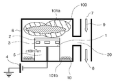
- FIG. 1 is a schematic view showing a magnetron sputtering apparatus used in a method of producing metal fine particles according to a first embodiment of the present invention.
- FIG. 2 is a schematic view showing a magnetron sputtering apparatus used for the method of producing metal fine particles according to the second embodiment of the present invention.
- a copper-containing target (copper, copper-nickel, copper-cobalt, copper-silicon, copper-carbon, etc.), aluminum, magnesium, titanium, etc.
- the target containing the above is placed in the chamber of a sputtering apparatus (preferably a magnetron sputtering apparatus).
- plasma is generated in a state in which the pressure in the chamber is 13 Pa or more, preferably about 26 Pa, and metal microparticles uniformly generated in the gas phase are generated to generate metal microparticles.
- a discharge gas for example, a rare gas such as Ar gas
- conductive fine particles are produced by producing fine metal particles by the above-described method of producing fine metal particles and incorporating the fine metal particles in a paste material (such as an epoxy adhesive resin or a phenolic adhesive resin). Can be manufactured.
- a paste material such as an epoxy adhesive resin or a phenolic adhesive resin.
- a semiconductor substrate such as a silicon wafer or a glass substrate is mounted in a chamber of a sputtering apparatus, and metal fine particles generated as described above are deposited on the substrate to form a metal thin film wiring on the substrate.
- metal fine particles generated by the above-described method for forming metal fine particles are deposited on the substrate to form a metal thin film, and then the metal thin film is patterned using a normal photolithography technique.
- Metal thin film wiring can be formed.
- the inert gas helium, argon gas, krypton gas, nitrogen gas, etc.
- the corrosion of the chamber parts of the sputtering apparatus by the corrosive gas such as chlorine is suppressed. can do. Therefore, according to the present embodiment, maintenance work of the device as a countermeasure against corrosion, temperature management work and apparatus sequence management work can be omitted. Therefore, it is possible to produce metal microparticles, a paste containing the metal microparticles, and a metal thin film wiring safely and inexpensively.
- FIG. 1 is a schematic view showing a magnetron sputtering apparatus used in a method of producing metal fine particles according to a first embodiment of the present invention.
- a copper target is used as a target, and the case of producing copper fine particles is described as an example.
- the magnetron sputtering apparatus is disposed on a chamber 6, a target electrode 1 installed on the lower surface side of the chamber 6 via an insulating component 5, a DC power supply 4 connected to the target electrode 1, and a bottom surface in the chamber 6. And the recovery tray 10.
- the chamber 6 is provided with a gas inlet 7 for introducing a discharge gas, and a gas outlet 8 for exhausting an exhaust gas from the chamber 6.
- the gas inlet 7 and the gas outlet 8 communicate with each other, and are connected to the chamber 6 via the connection path 20. Thereby, the pressure in the chamber 6 is determined only by the diffusion of the gas.
- the cathode side of the DC power source 4 is connected to the target electrode 1, and the anode side is grounded.
- the target electrode 1 is disposed such that the surface to be sputtered faces upward, and the copper target 2 is placed on the surface to be sputtered.
- the target electrode 1 is provided with a cathode magnet 3 which causes a magnetic flux loop horizontal to the surface to be sputtered to be closed.
- the flux loop is generated for the purpose of trapping electrons on the surface of the copper target 2 when the plasma 100 is generated in the chamber 6.
- the flux loop may be single or plural.
- the inside of the chamber 6 is exhausted by the exhaust pump (not shown) connected to the gas exhaust port 8 until the base pressure in the chamber 6 becomes 1E-5 Pa or less.
- the pressure value in the chamber 6 when the gas introduction is not performed is confirmed using a pressure gauge (for example, a full range gauge, a crystal ion gauge, etc.) (not shown).
- a pressure gauge for example, a full range gauge, a crystal ion gauge, etc.
- the evacuation time can be shortened or the inside of the chamber 6 can be reduced by heating the vacuum parts in the chamber 6 by a heating mechanism (not shown) to make it easy to exhaust moisture and volatile impurities of the parts in the chamber 6. Cleaning can be achieved.
- the heating of the parts by the heating mechanism is stopped when the base pressure in the chamber 6 becomes 1E-5 Pa or less.
- a rare gas such as an inert gas such as Ar (argon) gas 9 is introduced from the gas inlet 7 as a discharge gas.
- the pressure in the chamber 6 is measured by a pressure gauge (for example, a diaphragm gauge or the like) not shown.
- the exhaust conductance is adjusted by a variable orifice (not shown) installed between the gas exhaust port 8 and an exhaust pump (not shown) so that the pressure in the chamber 6 becomes a desired pressure, for example 26 Pa.
- the DC power source 4 is turned on to apply a desired power, for example, 0.5 W / cm 2 to the target electrode 1 to generate plasma 100 in the chamber 6.
- a desired power for example, 0.5 W / cm 2
- the first point is to maintain the pressure in the chamber 6 at 13 Pa or more, preferably about 26 Pa, to increase the frequency with which the copper atoms and the copper microparticles 101a collide with the gas.
- the upper limit of the pressure in the chamber 6 is preferably about 26 Pa.
- the second point is that the distance from the target electrode 1 to the inner wall surface of the chamber 6 is, for example, 40 mm or more, preferably 100 mm or more. As a result, it is possible to secure a sufficient space where the copper atoms generated from the copper target 2 in the chamber 6 collide with the gas and lose energy.
- the gas inlet 7 and the gas outlet 8 are communicated with each other and connected to the chamber 6 via the connection path 20 so that the flow of the gas is not generated in the chamber 6. It is preferable to control the pressure in 6 mainly on gas diffusion.
- the DC power supply 4 is turned off to end the generation of the plasma 100.
- the copper fine particles 101a floating in the plasma 100 diffuse so as to spread out omnidirectionally than the region where the plasma was present.
- the omnidirectionally diffused copper fine particles 101a collide with the side wall and the upper wall of the chamber 6 and bounce off from the wall, adhere to the wall of the chamber 6 by static electricity, lose their speed in the space, It falls to the bottom of the chamber 6.
- a portion of the copper particulates 101 a enters the recovery tray 10 as a metal particulate recovery member disposed on the bottom of the chamber 6 and is accumulated in the recovery tray 10.
- the copper particulates accumulated in the recovery tray 10 will be referred to as "copper particulates 101b".
- the DC power supply 4 is repeatedly turned on / off to generate the copper microparticles 101a in the plasma 100 and all the copper microparticles 101a in a state where the generation of the plasma 100 is ended. Repeat azimuthal diffusion. As a result, many copper microparticles 101 b are accumulated in the recovery tray 10.
- the inert gas is introduced into the chamber 6 to open the chamber 6, whereby the copper microparticles 101b accumulated in the recovery tray 10 can be recovered.
- the copper fine particle 101b with uniform distribution of the diameter was able to be produced
- the diameter of the copper fine particles 101b was distributed in the range of 80 nm to 150 nm in the copper fine particles 101b of 80% by weight or more of all the copper fine particles 101b generated in the present example. As described above, according to this example, it is possible to produce copper fine particles having an excellent uniformity of diameter.
- FIG. 2 is a schematic view showing a magnetron sputtering apparatus used for the method of producing metal fine particles according to the second embodiment of the present invention. Also in this example, a copper target is used as a target, and the case of producing copper fine particles is described as an example.
- the magnetron sputtering apparatus includes a chamber 6, a target electrode 1 installed on the upper surface side in the chamber 6 via an insulating component 5, and a DC power source 4 connected to the target electrode 1. Further, on the bottom surface side in the chamber 6, a recovery substrate 14 for recovering copper fine particles generated in the chamber 6 and a substrate holder 16 for supporting the same are disposed.
- the substrate holder 16 has a holder 12 installed on the bottom of the chamber 6 and a stage 13 installed on the holder 12, and the recovery substrate 14 is mounted on the stage 13. .
- the chamber 6 is provided with a gas inlet 7 for introducing a discharge gas, and a gas outlet 8 for discharging an exhaust gas from the chamber 6.
- the gas inlet 7 and the gas outlet 8 communicate with each other, and are connected to the chamber 6 via the connection path 20. Thereby, the pressure in the chamber 6 is determined only by the diffusion of the gas.
- the cathode side of the DC power source 4 is connected to the target electrode 1, and the anode side is grounded.
- the target electrode 1 is disposed such that the surface to be sputtered faces downward, and the surface to be sputtered of the target electrode 1 faces the substrate 14 for recovery.
- a copper target 2 is attached to the surface to be sputtered.
- the target electrode 1 is provided with a cathode magnet 3 which causes a magnetic flux loop horizontal to the surface to be sputtered to be closed.
- the flux loop is generated for the purpose of trapping electrons on the surface of the copper target 2 when the plasma 100 is generated in the chamber 6.
- the flux loop may be single or plural.
- a shutter mechanism 15 is provided between the target electrode 1 in the chamber 6 and the substrate holder 16.
- the shutter mechanism 15 is configured to be able to perform an opening and closing operation.
- the first space in the chamber 6 in which the target electrode 1 is installed and the second space in which the substrate holder 16 is installed are disconnected from each other.
- the shutter mechanism 15 is open, the spaces communicate with each other.
- the shutter mechanism 15 divides the inside of the chamber 6 into the first space and the second space, and allows the first space and the second space to communicate with each other. Switch.
- the distance between the target electrode 1 and the shutter mechanism 15 is 40 mm or more, preferably 100 mm or more.
- the process of producing copper particulates 101a in the gas phase in the present embodiment is the same as that of the first embodiment. Therefore, in the present embodiment, only points different from the first embodiment will be described.
- the magnetron sputtering apparatus in the present embodiment is different from the first embodiment in that the recovery substrate 14 and the target electrode 1 face each other. Also in this embodiment, with the shutter mechanism 15 open, the DC power supply 4 is turned on to generate the plasma 100 in the chamber 6, and after the copper microparticles 101a are generated therein, the DC power supply 4 is turned off. Thus, the copper microparticles 101b can be accumulated on the recovery substrate. However, since the surface to be sputtered of the target electrode 1 faces the recovery substrate 14, the plasma 100 generated in the chamber 6 extends to the recovery substrate 14 when the shutter mechanism 15 is opened.
- the DC power source 4 when the DC power source 4 is repeatedly turned on / off in the same manner as described in the first embodiment in an attempt to recover a large amount of copper particles 101b, the copper particles 101b recovered on the recovery substrate 14 are generated It will be repeatedly exposed to the plasma 100 which repeats disappearing. In that case, there is a possibility that the copper microparticles 101 b collected on the collection substrate 14 may be bonded to each other under the influence of the plasma 100.
- the shutter mechanism 15 when the copper particles 101a are generated in the plasma 100, the shutter mechanism 15 is closed, and the space in which the target electrode 1 is installed and the space in which the substrate holder 16 is installed Cut off. Then, the shutter mechanism 15 is opened immediately before the DC power supply 4 is turned off, and the copper particles 101 b are accumulated on the recovery substrate 14 while the DC power supply 4 is turned off.
- the shutter mechanism 15 is closed just before that to shut off both the above-mentioned spaces again, and the copper microparticles on the substrate for recovery 14 by the plasma 100 It prevents the 101b from binding to each other.
- the copper fine particles produced in the first or second embodiment described above are dispersed and contained in a phenolic adhesive resin to produce an electrically anisotropic paste.
- this electrically anisotropic paste is disposed between the lead terminal of the liquid crystal panel and the lead terminal of the TAB film and both are adhered and fixed, it is possible to obtain a connection structure having good electrical conductivity and adhesiveness. did it.
- the silicon wafer substrate was disposed at a position where the copper microparticles 101b in the chamber 6 in the first or second embodiment described above were deposited, and the copper microparticles 101b were deposited thereon. Thereby, a copper thin film having a resistance lower than that of a general copper thin film could be formed on a silicon wafer substrate.
- the metal thin film was able to be formed on the silicon wafer substrate by patterning the metal thin film into a desired shape using a normal photolithographic technique.
Landscapes
- Engineering & Computer Science (AREA)
- Chemical & Material Sciences (AREA)
- Condensed Matter Physics & Semiconductors (AREA)
- General Physics & Mathematics (AREA)
- Mechanical Engineering (AREA)
- Metallurgy (AREA)
- Organic Chemistry (AREA)
- Physics & Mathematics (AREA)
- Chemical Kinetics & Catalysis (AREA)
- Materials Engineering (AREA)
- Manufacturing & Machinery (AREA)
- Computer Hardware Design (AREA)
- Microelectronics & Electronic Packaging (AREA)
- Power Engineering (AREA)
- Electrodes Of Semiconductors (AREA)
- Physical Vapour Deposition (AREA)
- Manufacture Of Metal Powder And Suspensions Thereof (AREA)
- Manufacturing Of Electric Cables (AREA)
Priority Applications (1)
| Application Number | Priority Date | Filing Date | Title |
|---|---|---|---|
| US12/836,906 US20100276275A1 (en) | 2008-01-22 | 2010-07-15 | Method of generating fine metal particles, method of manufacturing metal-containing paste, and method of forming thin metal film interconnection |
Applications Claiming Priority (2)
| Application Number | Priority Date | Filing Date | Title |
|---|---|---|---|
| JP2008-011801 | 2008-01-22 | ||
| JP2008011801A JP2009173975A (ja) | 2008-01-22 | 2008-01-22 | 金属微粒子の生成方法、金属含有ペーストの製造方法及び金属薄膜配線の形成方法 |
Related Child Applications (1)
| Application Number | Title | Priority Date | Filing Date |
|---|---|---|---|
| US12/836,906 Continuation US20100276275A1 (en) | 2008-01-22 | 2010-07-15 | Method of generating fine metal particles, method of manufacturing metal-containing paste, and method of forming thin metal film interconnection |
Publications (1)
| Publication Number | Publication Date |
|---|---|
| WO2009093596A1 true WO2009093596A1 (ja) | 2009-07-30 |
Family
ID=40901104
Family Applications (1)
| Application Number | Title | Priority Date | Filing Date |
|---|---|---|---|
| PCT/JP2009/050834 Ceased WO2009093596A1 (ja) | 2008-01-22 | 2009-01-21 | 金属微粒子の生成方法、金属含有ペーストの製造方法及び金属薄膜配線の形成方法 |
Country Status (3)
| Country | Link |
|---|---|
| US (1) | US20100276275A1 (enExample) |
| JP (1) | JP2009173975A (enExample) |
| WO (1) | WO2009093596A1 (enExample) |
Cited By (1)
| Publication number | Priority date | Publication date | Assignee | Title |
|---|---|---|---|---|
| GB2481860A (en) * | 2010-07-09 | 2012-01-11 | Mantis Deposition Ltd | Sputtering apparatus for producing nanoparticles |
Families Citing this family (2)
| Publication number | Priority date | Publication date | Assignee | Title |
|---|---|---|---|---|
| JP5166531B2 (ja) * | 2008-06-24 | 2013-03-21 | キヤノンアネルバ株式会社 | 磁場発生装置及びプラズマ処理装置 |
| JP5802811B1 (ja) * | 2014-08-27 | 2015-11-04 | 株式会社ジーエル・マテリアルズホールディングス | ナノ粒子の製造方法 |
Citations (1)
| Publication number | Priority date | Publication date | Assignee | Title |
|---|---|---|---|---|
| JP2003245540A (ja) * | 2002-02-25 | 2003-09-02 | Fuji Photo Film Co Ltd | 超微粒子の作製方法 |
Family Cites Families (3)
| Publication number | Priority date | Publication date | Assignee | Title |
|---|---|---|---|---|
| JPH0735564B2 (ja) * | 1989-08-24 | 1995-04-19 | ワイケイケイ株式会社 | 耐食性と密着性とに優れた金属表面薄膜の形成方法 |
| US6287435B1 (en) * | 1998-05-06 | 2001-09-11 | Tokyo Electron Limited | Method and apparatus for ionized physical vapor deposition |
| JP5324251B2 (ja) * | 2008-05-16 | 2013-10-23 | キヤノンアネルバ株式会社 | 基板保持装置 |
-
2008
- 2008-01-22 JP JP2008011801A patent/JP2009173975A/ja not_active Withdrawn
-
2009
- 2009-01-21 WO PCT/JP2009/050834 patent/WO2009093596A1/ja not_active Ceased
-
2010
- 2010-07-15 US US12/836,906 patent/US20100276275A1/en not_active Abandoned
Patent Citations (1)
| Publication number | Priority date | Publication date | Assignee | Title |
|---|---|---|---|---|
| JP2003245540A (ja) * | 2002-02-25 | 2003-09-02 | Fuji Photo Film Co Ltd | 超微粒子の作製方法 |
Non-Patent Citations (2)
| Title |
|---|
| KOICHI SASAKI ET AL.: "Ko Gus-atsu Magnetron Sputtering Plasma ni Okeru Do Biryushi no Kansoku", THE 52TH EXTENDED ABSTRACTS, JAPAN SOCIETY OF APPLIED PHYSICS AND RELATED SOCIETIES,, vol. 1, 29 March 2005 (2005-03-29), pages 177 * |
| N.NAFARIZAL ET AL.: "Laser Sanranho ni yoru Ko Gas-atsu Sputtering Plazma-chu no Do Biryushi Kansatsu", THE 68TH EXTENDED ABSTRACTS, JAPAN SOCIETY OF APPLIED PHYSICS AND RELATED SOCIETIES, SEPARATE, vol. 1, 4 September 2007 (2007-09-04), pages 167 * |
Cited By (1)
| Publication number | Priority date | Publication date | Assignee | Title |
|---|---|---|---|---|
| GB2481860A (en) * | 2010-07-09 | 2012-01-11 | Mantis Deposition Ltd | Sputtering apparatus for producing nanoparticles |
Also Published As
| Publication number | Publication date |
|---|---|
| JP2009173975A (ja) | 2009-08-06 |
| US20100276275A1 (en) | 2010-11-04 |
Similar Documents
| Publication | Publication Date | Title |
|---|---|---|
| JP5373905B2 (ja) | 成膜装置及び成膜方法 | |
| JP5373904B2 (ja) | 成膜装置 | |
| US5362372A (en) | Self cleaning collimator | |
| TW201115617A (en) | Carbon materials for carbon implantation | |
| CN102428209A (zh) | 成膜方法以及成膜装置 | |
| US20110048927A1 (en) | Sputtering apparatus and sputtering method | |
| JP5901762B2 (ja) | ハードマスクの製造方法 | |
| JPH10330932A (ja) | スパッタリング装置 | |
| TWI465598B (zh) | A cathode unit and a sputtering apparatus having the cathode unit | |
| WO2009093596A1 (ja) | 金属微粒子の生成方法、金属含有ペーストの製造方法及び金属薄膜配線の形成方法 | |
| JP2007150012A (ja) | プラズマ処理装置および方法 | |
| US20060057742A1 (en) | Method of forming CNT containing wiring material and sputtering target material used for the method | |
| CN113832439B (zh) | 一种薄膜制备方法和设备 | |
| JP2011256441A (ja) | スパッタリング方法 | |
| TWI520802B (zh) | Self - ion sputtering device | |
| CN105420679A (zh) | 一种孪生对靶磁控溅射制备覆铜陶瓷基板的装置及方法 | |
| JP5693175B2 (ja) | スパッタリング方法 | |
| CN116815141A (zh) | 物理气相沉积装置和方法 | |
| JP5265309B2 (ja) | スパッタリング方法 | |
| TWI220767B (en) | Ionized physical vapor deposition process and apparatus thereof | |
| CN105931960A (zh) | 一种刻蚀掺铝氧化锌薄膜的方法 | |
| JP2011179068A (ja) | 金属薄膜の形成方法 | |
| CN103796440A (zh) | 在绝缘金属板上形成导电线路的方法 | |
| JP7517911B2 (ja) | 成膜方法及びスパッタリング装置 | |
| KR20150077522A (ko) | 스퍼터링 장치 |
Legal Events
| Date | Code | Title | Description |
|---|---|---|---|
| 121 | Ep: the epo has been informed by wipo that ep was designated in this application |
Ref document number: 09704078 Country of ref document: EP Kind code of ref document: A1 |
|
| DPE1 | Request for preliminary examination filed after expiration of 19th month from priority date (pct application filed from 20040101) | ||
| NENP | Non-entry into the national phase |
Ref country code: DE |
|
| 122 | Ep: pct application non-entry in european phase |
Ref document number: 09704078 Country of ref document: EP Kind code of ref document: A1 |