WO2009093596A1 - Method for producing metal fine particle, method for producing metal-containing paste, and method for forming metal thin film wiring - Google Patents
Method for producing metal fine particle, method for producing metal-containing paste, and method for forming metal thin film wiring Download PDFInfo
- Publication number
- WO2009093596A1 WO2009093596A1 PCT/JP2009/050834 JP2009050834W WO2009093596A1 WO 2009093596 A1 WO2009093596 A1 WO 2009093596A1 JP 2009050834 W JP2009050834 W JP 2009050834W WO 2009093596 A1 WO2009093596 A1 WO 2009093596A1
- Authority
- WO
- WIPO (PCT)
- Prior art keywords
- chamber
- fine particles
- metal fine
- copper
- target
- Prior art date
Links
- 229910052751 metal Inorganic materials 0.000 title claims abstract description 66
- 239000002184 metal Substances 0.000 title claims abstract description 66
- 239000010419 fine particle Substances 0.000 title claims abstract description 57
- 238000000034 method Methods 0.000 title claims abstract description 33
- 238000004519 manufacturing process Methods 0.000 title claims description 19
- 239000010409 thin film Substances 0.000 title claims description 14
- RYGMFSIKBFXOCR-UHFFFAOYSA-N Copper Chemical compound [Cu] RYGMFSIKBFXOCR-UHFFFAOYSA-N 0.000 claims abstract description 70
- 229910052802 copper Inorganic materials 0.000 claims abstract description 65
- 239000010949 copper Substances 0.000 claims abstract description 65
- 238000004544 sputter deposition Methods 0.000 claims abstract description 13
- 239000000758 substrate Substances 0.000 claims description 28
- 239000011859 microparticle Substances 0.000 claims description 21
- 238000011084 recovery Methods 0.000 claims description 19
- 238000001755 magnetron sputter deposition Methods 0.000 claims description 16
- 239000000463 material Substances 0.000 claims description 4
- 239000007769 metal material Substances 0.000 claims description 3
- 238000007599 discharging Methods 0.000 claims description 2
- 238000000059 patterning Methods 0.000 claims description 2
- 238000000151 deposition Methods 0.000 claims 2
- 229910000881 Cu alloy Inorganic materials 0.000 claims 1
- KZBUYRJDOAKODT-UHFFFAOYSA-N Chlorine Chemical compound ClCl KZBUYRJDOAKODT-UHFFFAOYSA-N 0.000 abstract description 7
- 239000007789 gas Substances 0.000 description 41
- 239000002245 particle Substances 0.000 description 10
- 230000004907 flux Effects 0.000 description 6
- 239000002923 metal particle Substances 0.000 description 5
- XKRFYHLGVUSROY-UHFFFAOYSA-N Argon Chemical compound [Ar] XKRFYHLGVUSROY-UHFFFAOYSA-N 0.000 description 4
- XUIMIQQOPSSXEZ-UHFFFAOYSA-N Silicon Chemical compound [Si] XUIMIQQOPSSXEZ-UHFFFAOYSA-N 0.000 description 4
- 238000009792 diffusion process Methods 0.000 description 4
- 238000010438 heat treatment Methods 0.000 description 4
- 229910052710 silicon Inorganic materials 0.000 description 4
- 239000010703 silicon Substances 0.000 description 4
- ZAMOUSCENKQFHK-UHFFFAOYSA-N Chlorine atom Chemical compound [Cl] ZAMOUSCENKQFHK-UHFFFAOYSA-N 0.000 description 3
- 229910001111 Fine metal Inorganic materials 0.000 description 3
- 239000004840 adhesive resin Substances 0.000 description 3
- 239000000460 chlorine Substances 0.000 description 3
- 229910052801 chlorine Inorganic materials 0.000 description 3
- 239000011261 inert gas Substances 0.000 description 3
- 238000012423 maintenance Methods 0.000 description 3
- 239000002243 precursor Substances 0.000 description 3
- 229920006223 adhesive resin Polymers 0.000 description 2
- 229910052786 argon Inorganic materials 0.000 description 2
- 238000005260 corrosion Methods 0.000 description 2
- 230000007797 corrosion Effects 0.000 description 2
- 230000000694 effects Effects 0.000 description 2
- 150000002739 metals Chemical class 0.000 description 2
- ISWSIDIOOBJBQZ-UHFFFAOYSA-N phenol group Chemical group C1(=CC=CC=C1)O ISWSIDIOOBJBQZ-UHFFFAOYSA-N 0.000 description 2
- 238000002360 preparation method Methods 0.000 description 2
- IJGRMHOSHXDMSA-UHFFFAOYSA-N Atomic nitrogen Chemical compound N#N IJGRMHOSHXDMSA-UHFFFAOYSA-N 0.000 description 1
- 229910000570 Cupronickel Inorganic materials 0.000 description 1
- UFHFLCQGNIYNRP-UHFFFAOYSA-N Hydrogen Chemical compound [H][H] UFHFLCQGNIYNRP-UHFFFAOYSA-N 0.000 description 1
- YZCKVEUIGOORGS-UHFFFAOYSA-N Hydrogen atom Chemical compound [H] YZCKVEUIGOORGS-UHFFFAOYSA-N 0.000 description 1
- FYYHWMGAXLPEAU-UHFFFAOYSA-N Magnesium Chemical compound [Mg] FYYHWMGAXLPEAU-UHFFFAOYSA-N 0.000 description 1
- RTAQQCXQSZGOHL-UHFFFAOYSA-N Titanium Chemical compound [Ti] RTAQQCXQSZGOHL-UHFFFAOYSA-N 0.000 description 1
- 229910052782 aluminium Inorganic materials 0.000 description 1
- XAGFODPZIPBFFR-UHFFFAOYSA-N aluminium Chemical compound [Al] XAGFODPZIPBFFR-UHFFFAOYSA-N 0.000 description 1
- 238000005266 casting Methods 0.000 description 1
- 238000004140 cleaning Methods 0.000 description 1
- RYTYSMSQNNBZDP-UHFFFAOYSA-N cobalt copper Chemical compound [Co].[Cu] RYTYSMSQNNBZDP-UHFFFAOYSA-N 0.000 description 1
- YOCUPQPZWBBYIX-UHFFFAOYSA-N copper nickel Chemical compound [Ni].[Cu] YOCUPQPZWBBYIX-UHFFFAOYSA-N 0.000 description 1
- WCCJDBZJUYKDBF-UHFFFAOYSA-N copper silicon Chemical compound [Si].[Cu] WCCJDBZJUYKDBF-UHFFFAOYSA-N 0.000 description 1
- 239000013078 crystal Substances 0.000 description 1
- 229910001873 dinitrogen Inorganic materials 0.000 description 1
- 230000005611 electricity Effects 0.000 description 1
- 230000002708 enhancing effect Effects 0.000 description 1
- 229920006332 epoxy adhesive Polymers 0.000 description 1
- -1 etc.) Chemical compound 0.000 description 1
- 238000001704 evaporation Methods 0.000 description 1
- 239000010408 film Substances 0.000 description 1
- 238000005242 forging Methods 0.000 description 1
- 239000011521 glass Substances 0.000 description 1
- 239000001307 helium Substances 0.000 description 1
- 229910052734 helium Inorganic materials 0.000 description 1
- SWQJXJOGLNCZEY-UHFFFAOYSA-N helium atom Chemical compound [He] SWQJXJOGLNCZEY-UHFFFAOYSA-N 0.000 description 1
- 239000001257 hydrogen Substances 0.000 description 1
- 229910052739 hydrogen Inorganic materials 0.000 description 1
- 239000012535 impurity Substances 0.000 description 1
- 230000001678 irradiating effect Effects 0.000 description 1
- 229910052743 krypton Inorganic materials 0.000 description 1
- DNNSSWSSYDEUBZ-UHFFFAOYSA-N krypton atom Chemical compound [Kr] DNNSSWSSYDEUBZ-UHFFFAOYSA-N 0.000 description 1
- 239000004973 liquid crystal related substance Substances 0.000 description 1
- 229910052749 magnesium Inorganic materials 0.000 description 1
- 239000011777 magnesium Substances 0.000 description 1
- AHADSRNLHOHMQK-UHFFFAOYSA-N methylidenecopper Chemical compound [Cu].[C] AHADSRNLHOHMQK-UHFFFAOYSA-N 0.000 description 1
- 238000012986 modification Methods 0.000 description 1
- 230000004048 modification Effects 0.000 description 1
- 238000000206 photolithography Methods 0.000 description 1
- 239000000843 powder Substances 0.000 description 1
- 238000004663 powder metallurgy Methods 0.000 description 1
- 239000004065 semiconductor Substances 0.000 description 1
- 230000003068 static effect Effects 0.000 description 1
- 239000010936 titanium Substances 0.000 description 1
- 229910052719 titanium Inorganic materials 0.000 description 1
- 231100000331 toxic Toxicity 0.000 description 1
- 230000002588 toxic effect Effects 0.000 description 1
- 239000011882 ultra-fine particle Substances 0.000 description 1
- 238000009827 uniform distribution Methods 0.000 description 1
Images

Classifications
-
- C—CHEMISTRY; METALLURGY
- C23—COATING METALLIC MATERIAL; COATING MATERIAL WITH METALLIC MATERIAL; CHEMICAL SURFACE TREATMENT; DIFFUSION TREATMENT OF METALLIC MATERIAL; COATING BY VACUUM EVAPORATION, BY SPUTTERING, BY ION IMPLANTATION OR BY CHEMICAL VAPOUR DEPOSITION, IN GENERAL; INHIBITING CORROSION OF METALLIC MATERIAL OR INCRUSTATION IN GENERAL
- C23C—COATING METALLIC MATERIAL; COATING MATERIAL WITH METALLIC MATERIAL; SURFACE TREATMENT OF METALLIC MATERIAL BY DIFFUSION INTO THE SURFACE, BY CHEMICAL CONVERSION OR SUBSTITUTION; COATING BY VACUUM EVAPORATION, BY SPUTTERING, BY ION IMPLANTATION OR BY CHEMICAL VAPOUR DEPOSITION, IN GENERAL
- C23C14/00—Coating by vacuum evaporation, by sputtering or by ion implantation of the coating forming material
- C23C14/06—Coating by vacuum evaporation, by sputtering or by ion implantation of the coating forming material characterised by the coating material
- C23C14/14—Metallic material, boron or silicon
- C23C14/16—Metallic material, boron or silicon on metallic substrates or on substrates of boron or silicon
- C23C14/165—Metallic material, boron or silicon on metallic substrates or on substrates of boron or silicon by cathodic sputtering
-
- B—PERFORMING OPERATIONS; TRANSPORTING
- B22—CASTING; POWDER METALLURGY
- B22F—WORKING METALLIC POWDER; MANUFACTURE OF ARTICLES FROM METALLIC POWDER; MAKING METALLIC POWDER; APPARATUS OR DEVICES SPECIALLY ADAPTED FOR METALLIC POWDER
- B22F9/00—Making metallic powder or suspensions thereof
- B22F9/02—Making metallic powder or suspensions thereof using physical processes
- B22F9/12—Making metallic powder or suspensions thereof using physical processes starting from gaseous material
-
- H—ELECTRICITY
- H01—ELECTRIC ELEMENTS
- H01L—SEMICONDUCTOR DEVICES NOT COVERED BY CLASS H10
- H01L21/00—Processes or apparatus adapted for the manufacture or treatment of semiconductor or solid state devices or of parts thereof
- H01L21/02—Manufacture or treatment of semiconductor devices or of parts thereof
- H01L21/04—Manufacture or treatment of semiconductor devices or of parts thereof the devices having potential barriers, e.g. a PN junction, depletion layer or carrier concentration layer
- H01L21/18—Manufacture or treatment of semiconductor devices or of parts thereof the devices having potential barriers, e.g. a PN junction, depletion layer or carrier concentration layer the devices having semiconductor bodies comprising elements of Group IV of the Periodic Table or AIIIBV compounds with or without impurities, e.g. doping materials
- H01L21/28—Manufacture of electrodes on semiconductor bodies using processes or apparatus not provided for in groups H01L21/20 - H01L21/268
- H01L21/283—Deposition of conductive or insulating materials for electrodes conducting electric current
- H01L21/285—Deposition of conductive or insulating materials for electrodes conducting electric current from a gas or vapour, e.g. condensation
- H01L21/28506—Deposition of conductive or insulating materials for electrodes conducting electric current from a gas or vapour, e.g. condensation of conductive layers
- H01L21/28512—Deposition of conductive or insulating materials for electrodes conducting electric current from a gas or vapour, e.g. condensation of conductive layers on semiconductor bodies comprising elements of Group IV of the Periodic Table
- H01L21/2855—Deposition of conductive or insulating materials for electrodes conducting electric current from a gas or vapour, e.g. condensation of conductive layers on semiconductor bodies comprising elements of Group IV of the Periodic Table by physical means, e.g. sputtering, evaporation
-
- B—PERFORMING OPERATIONS; TRANSPORTING
- B22—CASTING; POWDER METALLURGY
- B22F—WORKING METALLIC POWDER; MANUFACTURE OF ARTICLES FROM METALLIC POWDER; MAKING METALLIC POWDER; APPARATUS OR DEVICES SPECIALLY ADAPTED FOR METALLIC POWDER
- B22F2998/00—Supplementary information concerning processes or compositions relating to powder metallurgy
-
- B—PERFORMING OPERATIONS; TRANSPORTING
- B22—CASTING; POWDER METALLURGY
- B22F—WORKING METALLIC POWDER; MANUFACTURE OF ARTICLES FROM METALLIC POWDER; MAKING METALLIC POWDER; APPARATUS OR DEVICES SPECIALLY ADAPTED FOR METALLIC POWDER
- B22F2999/00—Aspects linked to processes or compositions used in powder metallurgy
Definitions
- the present invention relates to a method of producing metal particles, a method of producing a metal-containing paste, and a method of producing a metal thin film wiring.
- conductive pastes are used as the leads of many electronic devices. Copper particles are mainly dispersed in the conductive paste, and by evaporating volatile components of the paste, a wire of any shape can be produced. With the further miniaturization of electronic parts in recent years, thinning of the conductive paste is required, but for that purpose, it is necessary to reduce the particle size of copper particles in the conductive paste. .
- Patent Document 1 As a method of producing metal fine particles, a method as shown in Patent Document 1 is known. According to the method disclosed in Patent Document 1, a precursor of a copper component and chlorine is produced by chlorine and a copper member, the produced precursor is deposited on a substrate, and then a hydrogen-containing reducing gas is used. By irradiating the precursor with atomic hydrogen of the above, copper ultrafine particles are formed on the substrate. JP 2001-335959 A
- an object of the present invention is to provide a method etc. which produce metal particulate safely and cheaply.
- a target made of a metal material is placed in a chamber of a sputtering apparatus, and plasma is applied in the chamber under a pressure of 13 Pa or more in the chamber.
- the method is characterized in that metal fine particles are generated by generating and sputtering the target.
- metal particles can be produced safely and inexpensively.
- the present invention can produce fine particles of various metals.
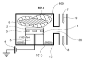
- FIG. 1 is a schematic view showing a magnetron sputtering apparatus used in a method of producing metal fine particles according to a first embodiment of the present invention.
- FIG. 2 is a schematic view showing a magnetron sputtering apparatus used for the method of producing metal fine particles according to the second embodiment of the present invention.
- a copper-containing target (copper, copper-nickel, copper-cobalt, copper-silicon, copper-carbon, etc.), aluminum, magnesium, titanium, etc.
- the target containing the above is placed in the chamber of a sputtering apparatus (preferably a magnetron sputtering apparatus).
- plasma is generated in a state in which the pressure in the chamber is 13 Pa or more, preferably about 26 Pa, and metal microparticles uniformly generated in the gas phase are generated to generate metal microparticles.
- a discharge gas for example, a rare gas such as Ar gas
- conductive fine particles are produced by producing fine metal particles by the above-described method of producing fine metal particles and incorporating the fine metal particles in a paste material (such as an epoxy adhesive resin or a phenolic adhesive resin). Can be manufactured.
- a paste material such as an epoxy adhesive resin or a phenolic adhesive resin.
- a semiconductor substrate such as a silicon wafer or a glass substrate is mounted in a chamber of a sputtering apparatus, and metal fine particles generated as described above are deposited on the substrate to form a metal thin film wiring on the substrate.
- metal fine particles generated by the above-described method for forming metal fine particles are deposited on the substrate to form a metal thin film, and then the metal thin film is patterned using a normal photolithography technique.
- Metal thin film wiring can be formed.
- the inert gas helium, argon gas, krypton gas, nitrogen gas, etc.
- the corrosion of the chamber parts of the sputtering apparatus by the corrosive gas such as chlorine is suppressed. can do. Therefore, according to the present embodiment, maintenance work of the device as a countermeasure against corrosion, temperature management work and apparatus sequence management work can be omitted. Therefore, it is possible to produce metal microparticles, a paste containing the metal microparticles, and a metal thin film wiring safely and inexpensively.
- FIG. 1 is a schematic view showing a magnetron sputtering apparatus used in a method of producing metal fine particles according to a first embodiment of the present invention.
- a copper target is used as a target, and the case of producing copper fine particles is described as an example.
- the magnetron sputtering apparatus is disposed on a chamber 6, a target electrode 1 installed on the lower surface side of the chamber 6 via an insulating component 5, a DC power supply 4 connected to the target electrode 1, and a bottom surface in the chamber 6. And the recovery tray 10.
- the chamber 6 is provided with a gas inlet 7 for introducing a discharge gas, and a gas outlet 8 for exhausting an exhaust gas from the chamber 6.
- the gas inlet 7 and the gas outlet 8 communicate with each other, and are connected to the chamber 6 via the connection path 20. Thereby, the pressure in the chamber 6 is determined only by the diffusion of the gas.
- the cathode side of the DC power source 4 is connected to the target electrode 1, and the anode side is grounded.
- the target electrode 1 is disposed such that the surface to be sputtered faces upward, and the copper target 2 is placed on the surface to be sputtered.
- the target electrode 1 is provided with a cathode magnet 3 which causes a magnetic flux loop horizontal to the surface to be sputtered to be closed.
- the flux loop is generated for the purpose of trapping electrons on the surface of the copper target 2 when the plasma 100 is generated in the chamber 6.
- the flux loop may be single or plural.
- the inside of the chamber 6 is exhausted by the exhaust pump (not shown) connected to the gas exhaust port 8 until the base pressure in the chamber 6 becomes 1E-5 Pa or less.
- the pressure value in the chamber 6 when the gas introduction is not performed is confirmed using a pressure gauge (for example, a full range gauge, a crystal ion gauge, etc.) (not shown).
- a pressure gauge for example, a full range gauge, a crystal ion gauge, etc.
- the evacuation time can be shortened or the inside of the chamber 6 can be reduced by heating the vacuum parts in the chamber 6 by a heating mechanism (not shown) to make it easy to exhaust moisture and volatile impurities of the parts in the chamber 6. Cleaning can be achieved.
- the heating of the parts by the heating mechanism is stopped when the base pressure in the chamber 6 becomes 1E-5 Pa or less.
- a rare gas such as an inert gas such as Ar (argon) gas 9 is introduced from the gas inlet 7 as a discharge gas.
- the pressure in the chamber 6 is measured by a pressure gauge (for example, a diaphragm gauge or the like) not shown.
- the exhaust conductance is adjusted by a variable orifice (not shown) installed between the gas exhaust port 8 and an exhaust pump (not shown) so that the pressure in the chamber 6 becomes a desired pressure, for example 26 Pa.
- the DC power source 4 is turned on to apply a desired power, for example, 0.5 W / cm 2 to the target electrode 1 to generate plasma 100 in the chamber 6.
- a desired power for example, 0.5 W / cm 2
- the first point is to maintain the pressure in the chamber 6 at 13 Pa or more, preferably about 26 Pa, to increase the frequency with which the copper atoms and the copper microparticles 101a collide with the gas.
- the upper limit of the pressure in the chamber 6 is preferably about 26 Pa.
- the second point is that the distance from the target electrode 1 to the inner wall surface of the chamber 6 is, for example, 40 mm or more, preferably 100 mm or more. As a result, it is possible to secure a sufficient space where the copper atoms generated from the copper target 2 in the chamber 6 collide with the gas and lose energy.
- the gas inlet 7 and the gas outlet 8 are communicated with each other and connected to the chamber 6 via the connection path 20 so that the flow of the gas is not generated in the chamber 6. It is preferable to control the pressure in 6 mainly on gas diffusion.
- the DC power supply 4 is turned off to end the generation of the plasma 100.
- the copper fine particles 101a floating in the plasma 100 diffuse so as to spread out omnidirectionally than the region where the plasma was present.
- the omnidirectionally diffused copper fine particles 101a collide with the side wall and the upper wall of the chamber 6 and bounce off from the wall, adhere to the wall of the chamber 6 by static electricity, lose their speed in the space, It falls to the bottom of the chamber 6.
- a portion of the copper particulates 101 a enters the recovery tray 10 as a metal particulate recovery member disposed on the bottom of the chamber 6 and is accumulated in the recovery tray 10.
- the copper particulates accumulated in the recovery tray 10 will be referred to as "copper particulates 101b".
- the DC power supply 4 is repeatedly turned on / off to generate the copper microparticles 101a in the plasma 100 and all the copper microparticles 101a in a state where the generation of the plasma 100 is ended. Repeat azimuthal diffusion. As a result, many copper microparticles 101 b are accumulated in the recovery tray 10.
- the inert gas is introduced into the chamber 6 to open the chamber 6, whereby the copper microparticles 101b accumulated in the recovery tray 10 can be recovered.
- the copper fine particle 101b with uniform distribution of the diameter was able to be produced
- the diameter of the copper fine particles 101b was distributed in the range of 80 nm to 150 nm in the copper fine particles 101b of 80% by weight or more of all the copper fine particles 101b generated in the present example. As described above, according to this example, it is possible to produce copper fine particles having an excellent uniformity of diameter.
- FIG. 2 is a schematic view showing a magnetron sputtering apparatus used for the method of producing metal fine particles according to the second embodiment of the present invention. Also in this example, a copper target is used as a target, and the case of producing copper fine particles is described as an example.
- the magnetron sputtering apparatus includes a chamber 6, a target electrode 1 installed on the upper surface side in the chamber 6 via an insulating component 5, and a DC power source 4 connected to the target electrode 1. Further, on the bottom surface side in the chamber 6, a recovery substrate 14 for recovering copper fine particles generated in the chamber 6 and a substrate holder 16 for supporting the same are disposed.
- the substrate holder 16 has a holder 12 installed on the bottom of the chamber 6 and a stage 13 installed on the holder 12, and the recovery substrate 14 is mounted on the stage 13. .
- the chamber 6 is provided with a gas inlet 7 for introducing a discharge gas, and a gas outlet 8 for discharging an exhaust gas from the chamber 6.
- the gas inlet 7 and the gas outlet 8 communicate with each other, and are connected to the chamber 6 via the connection path 20. Thereby, the pressure in the chamber 6 is determined only by the diffusion of the gas.
- the cathode side of the DC power source 4 is connected to the target electrode 1, and the anode side is grounded.
- the target electrode 1 is disposed such that the surface to be sputtered faces downward, and the surface to be sputtered of the target electrode 1 faces the substrate 14 for recovery.
- a copper target 2 is attached to the surface to be sputtered.
- the target electrode 1 is provided with a cathode magnet 3 which causes a magnetic flux loop horizontal to the surface to be sputtered to be closed.
- the flux loop is generated for the purpose of trapping electrons on the surface of the copper target 2 when the plasma 100 is generated in the chamber 6.
- the flux loop may be single or plural.
- a shutter mechanism 15 is provided between the target electrode 1 in the chamber 6 and the substrate holder 16.
- the shutter mechanism 15 is configured to be able to perform an opening and closing operation.
- the first space in the chamber 6 in which the target electrode 1 is installed and the second space in which the substrate holder 16 is installed are disconnected from each other.
- the shutter mechanism 15 is open, the spaces communicate with each other.
- the shutter mechanism 15 divides the inside of the chamber 6 into the first space and the second space, and allows the first space and the second space to communicate with each other. Switch.
- the distance between the target electrode 1 and the shutter mechanism 15 is 40 mm or more, preferably 100 mm or more.
- the process of producing copper particulates 101a in the gas phase in the present embodiment is the same as that of the first embodiment. Therefore, in the present embodiment, only points different from the first embodiment will be described.
- the magnetron sputtering apparatus in the present embodiment is different from the first embodiment in that the recovery substrate 14 and the target electrode 1 face each other. Also in this embodiment, with the shutter mechanism 15 open, the DC power supply 4 is turned on to generate the plasma 100 in the chamber 6, and after the copper microparticles 101a are generated therein, the DC power supply 4 is turned off. Thus, the copper microparticles 101b can be accumulated on the recovery substrate. However, since the surface to be sputtered of the target electrode 1 faces the recovery substrate 14, the plasma 100 generated in the chamber 6 extends to the recovery substrate 14 when the shutter mechanism 15 is opened.
- the DC power source 4 when the DC power source 4 is repeatedly turned on / off in the same manner as described in the first embodiment in an attempt to recover a large amount of copper particles 101b, the copper particles 101b recovered on the recovery substrate 14 are generated It will be repeatedly exposed to the plasma 100 which repeats disappearing. In that case, there is a possibility that the copper microparticles 101 b collected on the collection substrate 14 may be bonded to each other under the influence of the plasma 100.
- the shutter mechanism 15 when the copper particles 101a are generated in the plasma 100, the shutter mechanism 15 is closed, and the space in which the target electrode 1 is installed and the space in which the substrate holder 16 is installed Cut off. Then, the shutter mechanism 15 is opened immediately before the DC power supply 4 is turned off, and the copper particles 101 b are accumulated on the recovery substrate 14 while the DC power supply 4 is turned off.
- the shutter mechanism 15 is closed just before that to shut off both the above-mentioned spaces again, and the copper microparticles on the substrate for recovery 14 by the plasma 100 It prevents the 101b from binding to each other.
- the copper fine particles produced in the first or second embodiment described above are dispersed and contained in a phenolic adhesive resin to produce an electrically anisotropic paste.
- this electrically anisotropic paste is disposed between the lead terminal of the liquid crystal panel and the lead terminal of the TAB film and both are adhered and fixed, it is possible to obtain a connection structure having good electrical conductivity and adhesiveness. did it.
- the silicon wafer substrate was disposed at a position where the copper microparticles 101b in the chamber 6 in the first or second embodiment described above were deposited, and the copper microparticles 101b were deposited thereon. Thereby, a copper thin film having a resistance lower than that of a general copper thin film could be formed on a silicon wafer substrate.
- the metal thin film was able to be formed on the silicon wafer substrate by patterning the metal thin film into a desired shape using a normal photolithographic technique.
Landscapes
- Engineering & Computer Science (AREA)
- Chemical & Material Sciences (AREA)
- Condensed Matter Physics & Semiconductors (AREA)
- General Physics & Mathematics (AREA)
- Mechanical Engineering (AREA)
- Metallurgy (AREA)
- Organic Chemistry (AREA)
- Physics & Mathematics (AREA)
- Chemical Kinetics & Catalysis (AREA)
- Materials Engineering (AREA)
- Manufacturing & Machinery (AREA)
- Computer Hardware Design (AREA)
- Microelectronics & Electronic Packaging (AREA)
- Power Engineering (AREA)
- Electrodes Of Semiconductors (AREA)
- Physical Vapour Deposition (AREA)
- Manufacture Of Metal Powder And Suspensions Thereof (AREA)
- Manufacturing Of Electric Cables (AREA)
Abstract
Disclosed is a method for safely producing metal fine particles at low cost without using a chlorine gas. Specifically, copper fine particles (101a, 101b) are produced by sputtering a copper target (2), which is arranged in a chamber (6) of a sputtering apparatus, by generating a plasma (100) in the chamber (6) while setting the pressure within the chamber (6) to not less than 13 Pa.
Description
本発明は、金属粒子の生成方法、金属含有ペーストの製造方法及び金属薄膜配線の形成方法に関する。
The present invention relates to a method of producing metal particles, a method of producing a metal-containing paste, and a method of producing a metal thin film wiring.
近年、金属微粒子が様々な分野で応用されており、粒径の小さな微粒子の製造が求められている。例えば、多くの電子機器の導線として導電性ペーストが使用されている。導電性ペーストの中には主に銅粒子が分散されており、ペーストの揮発成分を蒸発させることにより、任意の形状の導線を作製することができる。近年における電子部品の更なる小型化に伴って、この導電性ペーストの薄膜化が求められているが、そのためには導電性ペースト中の銅粒子の粒径を小さくすることが必要とされている。
In recent years, metal fine particles have been applied in various fields, and production of fine particles having a small particle size is required. For example, conductive pastes are used as the leads of many electronic devices. Copper particles are mainly dispersed in the conductive paste, and by evaporating volatile components of the paste, a wire of any shape can be produced. With the further miniaturization of electronic parts in recent years, thinning of the conductive paste is required, but for that purpose, it is necessary to reduce the particle size of copper particles in the conductive paste. .
従来から、金属微粒子を生成する方法として特許文献1に示されるような方法が知られている。特許文献1に示された方法によれば、塩素と銅部材によって銅成分と塩素との前駆体を生成し、生成された前駆体を基板に成膜し、その後、水素を含有する還元ガスからの原子状水素を前駆体に照射することで、基板に銅超微粒子が形成される。
特開2001-335959号公報
Conventionally, as a method of producing metal fine particles, a method as shown in Patent Document 1 is known. According to the method disclosed in Patent Document 1, a precursor of a copper component and chlorine is produced by chlorine and a copper member, the produced precursor is deposited on a substrate, and then a hydrogen-containing reducing gas is used. By irradiating the precursor with atomic hydrogen of the above, copper ultrafine particles are formed on the substrate.
JP 2001-335959 A
上述した従来技術では、金属微粒子の形成方法を行うために、腐食性及び毒性の高い塩素ガスを使用する必要がある。その一方で、通常、チャンバーを形成する部材には強度の観点から金属部品が使用される。しかしながら、塩素ガスを使用する場合、装置のメンテナンス、温度管理、装置シーケンス等を駆使して装置管理を十分に行わないと、チャンバーの金属部品が腐食して塩素ガスが漏れたり、生成物が腐食したりするおそれがある。ところが、装置のメンテナンス、温度管理、装置シーケンス等を充実させることは、金属微粒子のコストを増大させる原因となる。
In the prior art described above, it is necessary to use highly corrosive and highly toxic chlorine gas in order to carry out the method of forming metal fine particles. On the other hand, metal components are generally used for the members forming the chamber in terms of strength. However, if chlorine gas is used, the metal parts of the chamber may be corroded to leak chlorine gas or the product may not be corroded unless the equipment management is carried out sufficiently using equipment maintenance, temperature control, equipment sequence, etc. There is a risk of However, enhancing the maintenance of the device, the temperature control, the device sequence and the like causes the cost of the metal fine particles to increase.
そこで本発明は、金属微粒子を安全にかつ安価に生成する方法等を提供することを目的とする。
Then, an object of the present invention is to provide a method etc. which produce metal particulate safely and cheaply.
上記目的を達成するため、本発明の金属微粒子の生成方法は、スパッタ装置のチャンバー内に金属材料からなるターゲットを設置し、前記チャンバー内の圧力を13Pa以上とした状態で前記チャンバー内にプラズマを生成して前記ターゲットをスパッタすることにより金属微粒子を生成することを特徴とする。
In order to achieve the above object, according to the method for producing metal fine particles of the present invention, a target made of a metal material is placed in a chamber of a sputtering apparatus, and plasma is applied in the chamber under a pressure of 13 Pa or more in the chamber. The method is characterized in that metal fine particles are generated by generating and sputtering the target.
本発明によれば、金属微粒子を安全にかつ安価に生成することができる。また、本発明は種々の金属の微粒子を製造可能である。
According to the present invention, metal particles can be produced safely and inexpensively. In addition, the present invention can produce fine particles of various metals.
添付図面は明細書に含まれ、その一部を構成し、本発明の実施の形態を示し、その記述を共に本発明の原理を説明するために用いられる。
図1は、本発明の第1の実施例に係る金属微粒子の生成方法に使用するマグネトロンスパッタ装置を示す概略図である。
図2は、本発明の第2の実施例に係る金属微粒子の生成方法に使用するマグネトロンスパッタ装置を示す概略図である。
BRIEF DESCRIPTION OF THE DRAWINGS The accompanying drawings are incorporated in and constitute a part of the specification to illustrate an embodiment of the invention and, together with the description, serve to explain the principles of the invention.
FIG. 1 is a schematic view showing a magnetron sputtering apparatus used in a method of producing metal fine particles according to a first embodiment of the present invention. FIG. 2 is a schematic view showing a magnetron sputtering apparatus used for the method of producing metal fine particles according to the second embodiment of the present invention.
以下、本発明の実施形態について詳細に説明する。ただし、この実施形態に記載されている構成要素はあくまで例示であり、本発明の技術的範囲は、請求の範囲によって確定されるのであって、以下の個別の実施形態によって限定されるわけではない。
Hereinafter, embodiments of the present invention will be described in detail. However, the components described in this embodiment are merely illustrative, and the technical scope of the present invention is determined by the scope of the claims, and is not limited by the following individual embodiments. .
本発明の一実施形態に係る金属微粒子の生成方法では、まず、たとえば銅を含有するターゲット(銅、銅・ニッケル、銅・コバルト、銅・シリコン、銅・炭素等)、アルミニウム、マグネシウム、チタンなどを含有するターゲットをスパッタ装置(好ましくはマグネトロンスパッタ装置)のチャンバー内に設置する。そして、チャンバー内の圧力を13Pa以上、好ましくは26Pa程度にした状態でプラズマを生成し、気相中に均一に分布した金属微粒子を発生させることで、金属微粒子を生成する。このとき、チャンバー内に放電用ガス(例えばArガス等の希ガス)を導入することが好ましい。
In the method for producing metal fine particles according to one embodiment of the present invention, first, for example, a copper-containing target (copper, copper-nickel, copper-cobalt, copper-silicon, copper-carbon, etc.), aluminum, magnesium, titanium, etc. The target containing the above is placed in the chamber of a sputtering apparatus (preferably a magnetron sputtering apparatus). Then, plasma is generated in a state in which the pressure in the chamber is 13 Pa or more, preferably about 26 Pa, and metal microparticles uniformly generated in the gas phase are generated to generate metal microparticles. At this time, it is preferable to introduce a discharge gas (for example, a rare gas such as Ar gas) into the chamber.
また、上述の金属微粒子の生成方法によって金属微粒子を生成し、その金属微粒子をペースト材(エポキシ系接着性樹脂やフェノール系接着性樹脂等)中に含有させることによって、電気異方性の導電ペーストを製造することができる。
In addition, conductive fine particles are produced by producing fine metal particles by the above-described method of producing fine metal particles and incorporating the fine metal particles in a paste material (such as an epoxy adhesive resin or a phenolic adhesive resin). Can be manufactured.
このほか、粉末冶金における粉末原料としても用いることができる。これにより、鍛造法や鋳造法などによる加工が困難な金属についても、精度が要求される加工品や微細な製品の製造が可能である。
Besides, it can also be used as a powder material in powder metallurgy. As a result, even for metals which are difficult to process by forging method, casting method or the like, it is possible to manufacture processed products and fine products which require accuracy.
さらに、スパッタ装置のチャンバー内にシリコンウエハー等の半導体基板やガラス基板を装着し、上記のようにして生成した金属微粒子をその基板の上に堆積させることによって、基板の上に金属薄膜配線を形成することもできる。具体的には、その基板の上に、上述の金属微粒子の生成方法によって生成した金属微粒子を堆積させて金属薄膜を形成させ、その後、通常のフォトリソグラフィー技術を用いてその金属薄膜をパターニングすることで、金属薄膜配線を形成することが可能である。
Furthermore, a semiconductor substrate such as a silicon wafer or a glass substrate is mounted in a chamber of a sputtering apparatus, and metal fine particles generated as described above are deposited on the substrate to form a metal thin film wiring on the substrate. You can also Specifically, metal fine particles generated by the above-described method for forming metal fine particles are deposited on the substrate to form a metal thin film, and then the metal thin film is patterned using a normal photolithography technique. Metal thin film wiring can be formed.
本実施形態によれば、プロセスガスとして不活性ガス(ヘリウム、アルゴンガス、クリプトンガス、窒素ガス等)が使用されるため、スパッタ装置のチャンバー部品が塩素等の腐食性ガスによって腐食することを抑制することができる。したがって、本実施形態によれば、腐食対策としての装置のメンテナンス作業、温度管理作業や装置シーケンス管理作業を省略することができる。そのため、金属微粒子、該金属微粒子を含有したペースト及び金属薄膜配線を安全にかつ安価に作製することが可能である。
According to the present embodiment, since the inert gas (helium, argon gas, krypton gas, nitrogen gas, etc.) is used as the process gas, the corrosion of the chamber parts of the sputtering apparatus by the corrosive gas such as chlorine is suppressed. can do. Therefore, according to the present embodiment, maintenance work of the device as a countermeasure against corrosion, temperature management work and apparatus sequence management work can be omitted. Therefore, it is possible to produce metal microparticles, a paste containing the metal microparticles, and a metal thin film wiring safely and inexpensively.
以下、本発明を実施例を参照して説明する。
The invention will now be described with reference to examples.
(第1の実施例)
図1は、本発明の第1の実施例に係る金属微粒子の生成方法に使用するマグネトロンスパッタ装置を示す概略図である。本実施例では、ターゲットとして銅ターゲットを用い、銅微粒子を生成する場合を例に挙げて説明する。 (First embodiment)
FIG. 1 is a schematic view showing a magnetron sputtering apparatus used in a method of producing metal fine particles according to a first embodiment of the present invention. In this embodiment, a copper target is used as a target, and the case of producing copper fine particles is described as an example.
まず、本実施例の金属微粒子の生成方法に使用するマグネトロンスパッタ装置の基本構成について説明する。このマグネトロンスパッタ装置は、チャンバー6と、チャンバー6内の下面側に絶縁部品5を介して設置されたターゲット電極1と、ターゲット電極1に接続されたDC電源4と、チャンバー6内の底面に配置された回収用トレー10とを有している。チャンバー6には、放電用ガスを導入するガス導入口7と、チャンバー6から排気ガスを排気するガス排気口8とが設けられている。ガス導入口7とガス排気口8とは互いに連通し、接続経路20を介してチャンバー6に接続されている。これにより、チャンバー6内の圧力がガスの拡散のみで決定されるようになっている。
First, the basic configuration of a magnetron sputtering apparatus used for the method of producing metal fine particles of the present embodiment will be described. The magnetron sputtering apparatus is disposed on a chamber 6, a target electrode 1 installed on the lower surface side of the chamber 6 via an insulating component 5, a DC power supply 4 connected to the target electrode 1, and a bottom surface in the chamber 6. And the recovery tray 10. The chamber 6 is provided with a gas inlet 7 for introducing a discharge gas, and a gas outlet 8 for exhausting an exhaust gas from the chamber 6. The gas inlet 7 and the gas outlet 8 communicate with each other, and are connected to the chamber 6 via the connection path 20. Thereby, the pressure in the chamber 6 is determined only by the diffusion of the gas.
DC電源4は、陰極側がターゲット電極1に接続され、陽極側が接地されている。ターゲット電極1は被スパッタ面が上方を向くように配置されており、その被スパッタ面上には銅ターゲット2が載置されている。ターゲット電極1には、被スパッタ面に対して水平な磁束ループを閉じるように生じさせるカソードマグネット3が設けられている。この磁束ループは、チャンバー6内にプラズマ100を生成したときに電子を銅ターゲット2の表面にトラップすることを目的として生成されるものである。磁束ループは単一でも複数でもよい。
The cathode side of the DC power source 4 is connected to the target electrode 1, and the anode side is grounded. The target electrode 1 is disposed such that the surface to be sputtered faces upward, and the copper target 2 is placed on the surface to be sputtered. The target electrode 1 is provided with a cathode magnet 3 which causes a magnetic flux loop horizontal to the surface to be sputtered to be closed. The flux loop is generated for the purpose of trapping electrons on the surface of the copper target 2 when the plasma 100 is generated in the chamber 6. The flux loop may be single or plural.
次に、上述したマグネトロンスパッタ装置の動作について説明する。
Next, the operation of the above-described magnetron sputtering apparatus will be described.
まず、銅微粒子を生成する準備として、ガス排気口8に接続されている不図示の排気ポンプによって、チャンバー6内のベース圧力が1E-5Pa以下となるまでチャンバー6内を排気する。ガス導入を行っていないときのチャンバー6内の圧力値は、不図示の圧力計(たとえばフルレンジゲージやクリスタルイオンゲージなど)を用いて確認する。なお、不図示の加熱機構によってチャンバー6内の真空部品を加熱して、チャンバー6内の部品の水分や気化性の不純物を排気しやすい状態にすることにより、排気時間の短縮やチャンバー6内の清浄化を図ることができる。加熱機構による部品の加熱は、チャンバー6内のベース圧力が1E-5Pa以下となった段階で停止する。以上により、銅微粒子を生成する準備が完了する。
First, in preparation for producing copper fine particles, the inside of the chamber 6 is exhausted by the exhaust pump (not shown) connected to the gas exhaust port 8 until the base pressure in the chamber 6 becomes 1E-5 Pa or less. The pressure value in the chamber 6 when the gas introduction is not performed is confirmed using a pressure gauge (for example, a full range gauge, a crystal ion gauge, etc.) (not shown). Note that the evacuation time can be shortened or the inside of the chamber 6 can be reduced by heating the vacuum parts in the chamber 6 by a heating mechanism (not shown) to make it easy to exhaust moisture and volatile impurities of the parts in the chamber 6. Cleaning can be achieved. The heating of the parts by the heating mechanism is stopped when the base pressure in the chamber 6 becomes 1E-5 Pa or less. Thus, preparation for producing copper fine particles is completed.
続いて、銅微粒子の生成について説明する。
Subsequently, generation of copper fine particles will be described.
まず、不活性ガスであるAr(アルゴン)ガス9等の希ガスを放電用ガスとしてガス導入口7から導入する。このとき、チャンバー6内の圧力を不図示の圧力計(たとえばダイヤフラムゲージ等)で測定する。そして、チャンバー6内の圧力が所望の圧力、たとえば26Paになるように、ガス排気口8と不図示の排気ポンプとの間に設置された不図示の可変オリフィスで排気コンダクタンスを調整する。所望の圧力に到達したところで、DC電源4をオンにして所望の電力、例えば0.5W/cm2をターゲット電極1に印加し、チャンバー6内にプラズマ100を生成させる。プラズマ100を生成した後、しばらくすると、銅ターゲット2からプラズマ100中に放出された銅原子が気相中に互いに結合し、プラズマ100中に銅微粒子101aが漂い始める。
First, a rare gas such as an inert gas such as Ar (argon) gas 9 is introduced from the gas inlet 7 as a discharge gas. At this time, the pressure in the chamber 6 is measured by a pressure gauge (for example, a diaphragm gauge or the like) not shown. Then, the exhaust conductance is adjusted by a variable orifice (not shown) installed between the gas exhaust port 8 and an exhaust pump (not shown) so that the pressure in the chamber 6 becomes a desired pressure, for example 26 Pa. When the desired pressure is reached, the DC power source 4 is turned on to apply a desired power, for example, 0.5 W / cm 2 to the target electrode 1 to generate plasma 100 in the chamber 6. After generating the plasma 100, for a while, copper atoms released from the copper target 2 into the plasma 100 bond to each other in the gas phase, and the copper particulates 101a begin to float in the plasma 100.
銅微粒子101aが気相中で成長するためには、銅原子の運動エネルギーをできるだけプラズマ100中で消失させ、銅原子を気相中にとどまらせて銅微粒子101aに成長させることが重要である。
In order for the copper particles 101a to grow in the gas phase, it is important to dissipate the kinetic energy of copper atoms in the plasma 100 as much as possible and keep the copper atoms in the gas phase to grow on the copper particles 101a.
そのための一つめのポイントは、チャンバー6内の圧力を13Pa以上、好ましくは26Pa程度に維持して、銅原子や銅微粒子101aがガスに衝突する頻度を増加させることである。チャンバー6内の圧力の上限は26Pa程度とすることが好ましい。
Therefore, the first point is to maintain the pressure in the chamber 6 at 13 Pa or more, preferably about 26 Pa, to increase the frequency with which the copper atoms and the copper microparticles 101a collide with the gas. The upper limit of the pressure in the chamber 6 is preferably about 26 Pa.
二つめのポイントは、ターゲット電極1からチャンバー6の内壁面までの距離をたとえば40mm以上、好ましくは100mm以上にすることである。これにより、チャンバー6内で銅ターゲット2からたたき出された銅原子がガスと衝突してエネルギーを消失する空間を十分に確保することができる。
The second point is that the distance from the target electrode 1 to the inner wall surface of the chamber 6 is, for example, 40 mm or more, preferably 100 mm or more. As a result, it is possible to secure a sufficient space where the copper atoms generated from the copper target 2 in the chamber 6 collide with the gas and lose energy.
さらに、銅微粒子101aが気相中で成長するためには、銅微粒子101aの漂うのを妨げない環境をつくることが重要である。そのために、チャンバー6内にガスの流れが発生しないように、上述したようにガス導入口7とガス排気口8とを互いに連通させて接続経路20を介してチャンバー6に接続させることで、チャンバー6内の圧力制御をガス拡散を主体として行うことが好ましい。
Furthermore, in order for the copper particulates 101a to grow in the gas phase, it is important to create an environment that does not prevent the copper particulates 101a from drifting. Therefore, as described above, the gas inlet 7 and the gas outlet 8 are communicated with each other and connected to the chamber 6 via the connection path 20 so that the flow of the gas is not generated in the chamber 6. It is preferable to control the pressure in 6 mainly on gas diffusion.
プラズマ100を生成させ、所定の時間放電を維持した後に、DC電源4をオフにしてプラズマ100の生成を終了する。DC電源4をオフにすると、プラズマ100中を漂っていた銅微粒子101aは、プラズマが存在していた領域よりも全方位的に外に広がるように拡散する。全方位的に拡散した銅微粒子101aは、チャンバー6の側壁や上壁に衝突してそれらの壁から跳ね返されたり、静電気によってチャンバー6の壁面に付着したり、空間中で速度を失って、そのままチャンバー6の底面に落下する。銅微粒子101aの一部は、チャンバー6の底面に設置されている金属微粒子回収部材としての回収用トレー10内に入り、回収用トレー10内に蓄積される。以下、回収用トレー10内に蓄積された銅微粒子を「銅微粒子101b」と称する。多くの銅微粒子101bを生成したい場合は、DC電源4のオン/オフを繰り返して、プラズマ100中での銅微粒子101aの生成と、プラズマ100の生成を終了させた状態での銅微粒子101aの全方位的な拡散とを繰り返し行う。これにより、回収用トレー10内に多くの銅微粒子101bが蓄積される。
After the plasma 100 is generated and discharge is maintained for a predetermined time, the DC power supply 4 is turned off to end the generation of the plasma 100. When the DC power supply 4 is turned off, the copper fine particles 101a floating in the plasma 100 diffuse so as to spread out omnidirectionally than the region where the plasma was present. The omnidirectionally diffused copper fine particles 101a collide with the side wall and the upper wall of the chamber 6 and bounce off from the wall, adhere to the wall of the chamber 6 by static electricity, lose their speed in the space, It falls to the bottom of the chamber 6. A portion of the copper particulates 101 a enters the recovery tray 10 as a metal particulate recovery member disposed on the bottom of the chamber 6 and is accumulated in the recovery tray 10. Hereinafter, the copper particulates accumulated in the recovery tray 10 will be referred to as "copper particulates 101b". When it is desired to generate many copper microparticles 101b, the DC power supply 4 is repeatedly turned on / off to generate the copper microparticles 101a in the plasma 100 and all the copper microparticles 101a in a state where the generation of the plasma 100 is ended. Repeat azimuthal diffusion. As a result, many copper microparticles 101 b are accumulated in the recovery tray 10.
最後に、チャンバー6内に不活性ガスを導入してチャンバー6を開放することにより、回収用トレー10内に蓄積された銅微粒子101bを回収することができる。
Finally, the inert gas is introduced into the chamber 6 to open the chamber 6, whereby the copper microparticles 101b accumulated in the recovery tray 10 can be recovered.
上述したように、本実施例の金属微粒子の生成方法によれば、塩素ガスを使用することなく銅微粒子を生成することが可能である。したがって、スパッタ装置の構成部材が塩素ガスによって腐食するおそれがないため、スパッタ装置の管理に要する手間を省くことができる。また、スパッタ装置のチャンバーから塩素ガスが漏れ出ることもない。そのため、銅微粒子の生成を安全にかつ安価に行うことができる。
As described above, according to the method for producing metal microparticles of the present embodiment, it is possible to produce copper microparticles without using chlorine gas. Therefore, since there is no possibility that the component members of the sputtering apparatus may be corroded by chlorine gas, it is possible to save time and effort required for managing the sputtering apparatus. In addition, chlorine gas does not leak from the chamber of the sputtering apparatus. Therefore, copper particulates can be generated safely and inexpensively.
また、本実施例によれば、直径の分布が均一な銅微粒子101bを生成することができた。具体的には、本実施例によって生成された全ての銅微粒子101bの80重量%以上の銅微粒子101bで、銅微粒子101bの直径が80nm~150nmの範囲に分布していた。このように、本実施例によれば、直径の均一度が優れた銅微粒子を生成することが出来た。
Moreover, according to the present Example, the copper fine particle 101b with uniform distribution of the diameter was able to be produced | generated. Specifically, the diameter of the copper fine particles 101b was distributed in the range of 80 nm to 150 nm in the copper fine particles 101b of 80% by weight or more of all the copper fine particles 101b generated in the present example. As described above, according to this example, it is possible to produce copper fine particles having an excellent uniformity of diameter.
(第2の実施例)
図2は、本発明の第2の実施例に係る金属微粒子の生成方法に使用するマグネトロンスパッタ装置を示す概略図である。本実施例においても、ターゲットとして銅ターゲットを用い、銅微粒子を生成する場合を例に挙げて説明する。 Second Embodiment
FIG. 2 is a schematic view showing a magnetron sputtering apparatus used for the method of producing metal fine particles according to the second embodiment of the present invention. Also in this example, a copper target is used as a target, and the case of producing copper fine particles is described as an example.
まず、本実施例の金属微粒子の生成方法に使用するマグネトロンスパッタ装置の基本構成について説明する。このマグネトロンスパッタ装置は、チャンバー6と、チャンバー6内の上面側に絶縁部品5を介して設置されたターゲット電極1と、ターゲット電極1に接続されたDC電源4とを有している。さらに、チャンバー6内の底面側には、チャンバー6内で生成された銅微粒子を回収する回収用基板14と、それを支持する基板ホルダー16とが配置されている。基板ホルダー16は、チャンバー6の底面の上に設置されたホルダー12と、ホルダー12の上に設置されたステージ13とを有しており、回収用基板14はステージ13の上に載せられている。
First, the basic configuration of a magnetron sputtering apparatus used for the method of producing metal fine particles of the present embodiment will be described. The magnetron sputtering apparatus includes a chamber 6, a target electrode 1 installed on the upper surface side in the chamber 6 via an insulating component 5, and a DC power source 4 connected to the target electrode 1. Further, on the bottom surface side in the chamber 6, a recovery substrate 14 for recovering copper fine particles generated in the chamber 6 and a substrate holder 16 for supporting the same are disposed. The substrate holder 16 has a holder 12 installed on the bottom of the chamber 6 and a stage 13 installed on the holder 12, and the recovery substrate 14 is mounted on the stage 13. .
チャンバー6には、放電用ガスを導入するガス導入口7と、チャンバー6から排気ガスを排出するガス排気口8とが設けられている。ガス導入口7とガス排気口8とは互いに連通し、接続経路20を介してチャンバー6に接続されている。これにより、チャンバー6内の圧力がガスの拡散のみで決定されるようになっている。
The chamber 6 is provided with a gas inlet 7 for introducing a discharge gas, and a gas outlet 8 for discharging an exhaust gas from the chamber 6. The gas inlet 7 and the gas outlet 8 communicate with each other, and are connected to the chamber 6 via the connection path 20. Thereby, the pressure in the chamber 6 is determined only by the diffusion of the gas.
DC電源4は、陰極側がターゲット電極1に接続され、陽極側が接地されている。ターゲット電極1は被スパッタ面が下方を向くように配置されており、ターゲット電極1の被スパッタ面は回収用基板14に対向している。その被スパッタ面には銅ターゲット2が取り付けられている。ターゲット電極1には、被スパッタ面に対して水平な磁束ループを閉じるように生じさせるカソードマグネット3が設けられている。この磁束ループは、チャンバー6内にプラズマ100を生成したときに電子を銅ターゲット2の表面にトラップすることを目的として生成されるものである。磁束ループは単一でも複数でもよい。
The cathode side of the DC power source 4 is connected to the target electrode 1, and the anode side is grounded. The target electrode 1 is disposed such that the surface to be sputtered faces downward, and the surface to be sputtered of the target electrode 1 faces the substrate 14 for recovery. A copper target 2 is attached to the surface to be sputtered. The target electrode 1 is provided with a cathode magnet 3 which causes a magnetic flux loop horizontal to the surface to be sputtered to be closed. The flux loop is generated for the purpose of trapping electrons on the surface of the copper target 2 when the plasma 100 is generated in the chamber 6. The flux loop may be single or plural.
さらに、本実施例におけるマグネトロンスパッタ装置では、チャンバー6内のターゲット電極1と基板ホルダー16との間にシャッター機構15が設けられている。シャッター機構15は開閉動作を行うことが可能な構成となっている。シャッター機構15が閉じた状態では、チャンバー6内のターゲット電極1が設置されている第1の空間と基板ホルダー16が設置されている第2の空間とが互いに遮断される。一方、シャッター機構15が開いた状態では、それらの空間が互いに連通した状態となる。このように、シャッター機構15は、チャンバー6内を上記の第1の空間と第2の空間とに仕切り、第1の空間と第2の空間とを連通させた状態と遮断させた状態とに切り替える。本実施例では、ターゲット電極1とシャッター機構15との距離は40mm以上好ましくは100mm以上である。
Furthermore, in the magnetron sputtering apparatus in the present embodiment, a shutter mechanism 15 is provided between the target electrode 1 in the chamber 6 and the substrate holder 16. The shutter mechanism 15 is configured to be able to perform an opening and closing operation. When the shutter mechanism 15 is closed, the first space in the chamber 6 in which the target electrode 1 is installed and the second space in which the substrate holder 16 is installed are disconnected from each other. On the other hand, when the shutter mechanism 15 is open, the spaces communicate with each other. As described above, the shutter mechanism 15 divides the inside of the chamber 6 into the first space and the second space, and allows the first space and the second space to communicate with each other. Switch. In the present embodiment, the distance between the target electrode 1 and the shutter mechanism 15 is 40 mm or more, preferably 100 mm or more.
第2の実施例で使用するマグネトロンスパッタ装置の動作について説明する。
The operation of the magnetron sputtering apparatus used in the second embodiment will be described.
本実施例における銅微粒子101aを気相中に生成する過程は第1の実施例と同様である。したがって、本実施例では第1の実施例と異なる点に焦点を絞って説明する。
The process of producing copper particulates 101a in the gas phase in the present embodiment is the same as that of the first embodiment. Therefore, in the present embodiment, only points different from the first embodiment will be described.
本実施例におけるマグネトロンスパッタ装置は、回収用基板14とターゲット電極1とが互いに対向している点において第1の実施例と異なる。本実施例でも、シャッター機構15を開いた状態で、DC電源4をオンにしてチャンバー6内にプラズマ100を発生させ、その中に銅微粒子101aを生成させた後にDC電源4をオフにすることで、回収用基板14上に銅微粒子101bを蓄積することが可能である。しかしながら、ターゲット電極1の被スパッタ面が回収用基板14に対向しているため、シャッター機構15を開いた状態ではチャンバー6内に生成されるプラズマ100が回収用基板14にも及ぶ。そのため、多量の銅微粒子101bを回収しようとして、第1の実施例で説明したのと同様にDC電源4のオン/オフを繰り返すと、回収用基板14に回収された銅微粒子101bは、生成と消失とを繰り返すプラズマ100に繰り返し曝されることとなる。その場合、回収用基板14に回収された銅微粒子101bがプラズマ100の影響で互いに結合してしまう可能性がある。
The magnetron sputtering apparatus in the present embodiment is different from the first embodiment in that the recovery substrate 14 and the target electrode 1 face each other. Also in this embodiment, with the shutter mechanism 15 open, the DC power supply 4 is turned on to generate the plasma 100 in the chamber 6, and after the copper microparticles 101a are generated therein, the DC power supply 4 is turned off. Thus, the copper microparticles 101b can be accumulated on the recovery substrate. However, since the surface to be sputtered of the target electrode 1 faces the recovery substrate 14, the plasma 100 generated in the chamber 6 extends to the recovery substrate 14 when the shutter mechanism 15 is opened. Therefore, when the DC power source 4 is repeatedly turned on / off in the same manner as described in the first embodiment in an attempt to recover a large amount of copper particles 101b, the copper particles 101b recovered on the recovery substrate 14 are generated It will be repeatedly exposed to the plasma 100 which repeats disappearing. In that case, there is a possibility that the copper microparticles 101 b collected on the collection substrate 14 may be bonded to each other under the influence of the plasma 100.
そこで本実施例では、プラズマ100中に銅微粒子101aを生成しているときは、シャッター機構15を閉じて、ターゲット電極1が設置されている空間と基板ホルダー16が設置されている空間とを互いに遮断する。そして、DC電源4をオフにする直前にシャッター機構15を開き、DC電源4をオフにしている間に銅微粒子101bが回収用基板14上に蓄積されるようにする。銅微粒子101aを生成するためにDC電源4を再びオンにするときは、その直前にシャッター機構15を閉じて上記の両空間を再び互いに遮断して、プラズマ100によって回収用基板14上の銅微粒子101b同士が結合することを防ぐ。
Therefore, in the present embodiment, when the copper particles 101a are generated in the plasma 100, the shutter mechanism 15 is closed, and the space in which the target electrode 1 is installed and the space in which the substrate holder 16 is installed Cut off. Then, the shutter mechanism 15 is opened immediately before the DC power supply 4 is turned off, and the copper particles 101 b are accumulated on the recovery substrate 14 while the DC power supply 4 is turned off. When the DC power supply 4 is turned on again to generate the copper microparticles 101a, the shutter mechanism 15 is closed just before that to shut off both the above-mentioned spaces again, and the copper microparticles on the substrate for recovery 14 by the plasma 100 It prevents the 101b from binding to each other.
なお、図2に示したマグネトロンスパッタ装置に回収用基板14を真空中で搬送する機構を追加すれば、チャンバー6を大気開放することなく銅微粒子101bを回収することが可能である。
Incidentally, if a mechanism for transporting the substrate for recovery 14 in vacuum is added to the magnetron sputtering apparatus shown in FIG. 2, it is possible to recover the copper particulates 101b without opening the chamber 6 to the atmosphere.
上述した第1及び第2の実施例では銅微粒子を生成する場合について説明したが、ターゲットの材料を銅から別の金属材料に変更すれば、他の金属微粒子を生成することができる。また、上述した各実施例ではターゲット電極1にDC電源4を接続したマグネトロンスパッタ装置を使用したが、ターゲット電極1にDC電源4の代わりにAC電源を接続してターゲット電極1に交流電力を印加しても、同様の作用効果を奏することが可能である。あるいは、ターゲット電極1にDC電源4とAC電源とを接続し、ターゲット電極1に直流電力と交流電力とを重畳的に印加しても、同様の作用効果を奏することが可能である。
In the first and second embodiments described above, the case of producing copper fine particles has been described, but if the material of the target is changed from copper to another metal material, other metal fine particles can be produced. Moreover, although the magnetron sputtering apparatus which connected DC power supply 4 to the target electrode 1 was used in each Example mentioned above, AC power supply is connected to the target electrode 1 instead of DC power supply 4, and AC power is applied to the target electrode 1 Even if it is, it is possible to produce the same effect. Alternatively, even if DC power supply 4 and AC power supply are connected to the target electrode 1 and DC power and AC power are applied to the target electrode 1 in a superimposed manner, the same operation and effect can be achieved.
(第3の実施例)
上述した第1又は第2の実施例で生成した銅微粒子をフェノール系接着樹脂中に分散含有させて、電気異方性ペーストを製造した。この電気異方性ペーストを、液晶パネルの導線端子部とTABフィルムの導線端子との間に配置して両者を接着固定したところ、電気的導通性および接着性が良好な接続構造を得ることができた。 Third Embodiment
The copper fine particles produced in the first or second embodiment described above are dispersed and contained in a phenolic adhesive resin to produce an electrically anisotropic paste. When this electrically anisotropic paste is disposed between the lead terminal of the liquid crystal panel and the lead terminal of the TAB film and both are adhered and fixed, it is possible to obtain a connection structure having good electrical conductivity and adhesiveness. did it.
(第4の実施例)
上述した第1又は第2の実施例におけるチャンバー6内の銅微粒子101bが堆積する位置にシリコンウエハー基板を配置し、その上に銅微粒子101bを堆積させた。これにより、一般的な銅薄膜よりも抵抗が低い銅薄膜をシリコンウエハー基板上に形成することができた。 Fourth Embodiment
The silicon wafer substrate was disposed at a position where thecopper microparticles 101b in the chamber 6 in the first or second embodiment described above were deposited, and the copper microparticles 101b were deposited thereon. Thereby, a copper thin film having a resistance lower than that of a general copper thin film could be formed on a silicon wafer substrate.
上述した第1又は第2の実施例におけるチャンバー6内の銅微粒子101bが堆積する位置にシリコンウエハー基板を配置し、その上に銅微粒子101bを堆積させた。これにより、一般的な銅薄膜よりも抵抗が低い銅薄膜をシリコンウエハー基板上に形成することができた。 Fourth Embodiment
The silicon wafer substrate was disposed at a position where the
そして、通常のフォトリソグラフィー技術を用いてその金属薄膜を所望の形状にパターニングすることで、シリコンウエハー基板上に金属薄膜配線を形成することができた。
Then, the metal thin film was able to be formed on the silicon wafer substrate by patterning the metal thin film into a desired shape using a normal photolithographic technique.
以上、本発明の好ましい実施形態を添付図面の参照により説明したが、本発明はかかる実施形態に限定されるものではなく、請求の範囲の記載から把握される技術的範囲において種々な形態に変更可能である。
Although the preferred embodiments of the present invention have been described above with reference to the accompanying drawings, the present invention is not limited to such embodiments, and various modifications may be made within the technical scope understood from the description of the claims. It is possible.
本願は、2008年1月22日提出の日本国特許出願特願2008-11801を基礎として優先権を主張するものであり、その記載内容の全てを、ここに援用する。
The present application claims priority based on Japanese Patent Application No. 2008-11801 filed on Jan. 22, 2008, the entire content of which is incorporated herein by reference.
Claims (14)
- 金属材料からなるターゲットをスパッタ装置のチャンバー内に設置し、
前記チャンバー内の圧力を13Pa以上とした状態で前記チャンバー内にプラズマを生成して前記ターゲットをスパッタすることにより金属微粒子を生成することを特徴とする、金属微粒子の生成方法。 Place a target made of a metal material in the chamber of the sputtering apparatus,
A method of producing metal fine particles, characterized in that metal fine particles are generated by generating plasma in the chamber and sputtering the target with the pressure in the chamber being 13 Pa or more. - 前記スパッタ装置としてマグネトロンスパッタ装置を用いる、請求項1に記載の金属微粒子の生成方法。 The method for producing metal fine particles according to claim 1, wherein a magnetron sputtering apparatus is used as the sputtering apparatus.
- 前記チャンバー内に放電用ガスを導入する、請求項1または2に記載の金属微粒子の生成方法。 The method for producing metal fine particles according to claim 1 or 2, wherein a gas for discharge is introduced into the chamber.
- 前記チャンバーには、前記チャンバー内に放電用ガスを導入するガス導入口と、前記チャンバーから放電用ガスを排気するガス排気口とが接続されている、請求項1から3のいずれか1項に記載の金属微粒子の生成方法。 The gas inlet for introducing a discharge gas into the chamber and a gas outlet for discharging the discharge gas from the chamber are connected to the chamber. Method for producing metal fine particles as described.
- 前記ガス導入口と前記ガス排気口とは互いに連通しており、前記ガス導入口及び前記ガス排気口は接続経路を介して前記チャンバーに接続されている、請求項4に記載の金属微粒子の生成方法。 5. The production of metal fine particles according to claim 4, wherein the gas inlet and the gas outlet are in communication with each other, and the gas inlet and the gas outlet are connected to the chamber via a connection path. Method.
- 前記ターゲットを、前記チャンバーの内壁面から40mm以上の距離をおいて前記チャンバー内に設置する、請求項1から5のいずれか1項に記載の金属微粒子の生成方法。 The method for producing metal fine particles according to any one of claims 1 to 5, wherein the target is placed in the chamber at a distance of 40 mm or more from an inner wall surface of the chamber.
- 前記金属微粒子を堆積させて回収する金属微粒子回収部材を前記チャンバー内に配置する、請求項1から6のいずれか1項に記載の金属微粒子の生成方法。 The method for producing metal fine particles according to any one of claims 1 to 6, wherein a metal fine particle collecting member for depositing and collecting the metal fine particles is disposed in the chamber.
- 前記金属微粒子回収部材を前記チャンバーの底面に配置する、請求項7に記載の金属微粒子の生成方法。 The method of producing metal fine particles according to claim 7, wherein the metal fine particle collecting member is disposed on the bottom of the chamber.
- 前記金属微粒子回収部材を、前記ターゲットの下方の前記ターゲットに対向する位置に配置する、請求項7に記載の金属微粒子の生成方法。 The method for producing metal fine particles according to claim 7, wherein the metal fine particle collecting member is disposed at a position facing the target below the target.
- 前記チャンバー内を、前記ターゲットが配置された第1の空間と前記金属微粒子回収部材が配置された第2の空間とに仕切り、前記第1の空間と前記第2の空間とを連通させた状態と遮断させた状態とに切り替えるシャッター機構を前記チャンバー内に設置する、請求項8に記載の金属微粒子の生成方法。 A state in which the inside of the chamber is partitioned into a first space in which the target is disposed and a second space in which the metal fine particle recovery member is disposed, and the first space and the second space are communicated. The method for producing metal fine particles according to claim 8, wherein a shutter mechanism that switches between and the shuttered state is installed in the chamber.
- 前記ターゲットと前記シャッター機構との間の距離を40mm以上とする、請求項10に記載の金属微粒子の生成方法。 The method according to claim 10, wherein a distance between the target and the shutter mechanism is 40 mm or more.
- 銅又は銅合金からなるターゲットを用いる、請求項1から11のいずれか1項に記載の金属微粒子の生成方法。 The method for producing metal fine particles according to any one of claims 1 to 11, wherein a target made of copper or a copper alloy is used.
- 請求項1から12のいずれか1項に記載の金属微粒子の生成方法によって生成された金属微粒子をペースト材に含有させる工程を有する、金属含有ペーストの製造方法。 The manufacturing method of the metal containing paste which has the process of making the paste material contain the metal microparticle produced | generated by the production | generation method of the metal microparticle of any one of Claims 1-12.
- 請求項1から12のいずれか1項に記載の金属微粒子の生成方法によって生成された金属微粒子を前記チャンバー内に設置した基板の上に堆積させて金属薄膜を形成する工程と、
前記金属薄膜をパターニングして配線を形成する工程と、
を有する、金属薄膜配線の形成方法。 Depositing metal fine particles produced by the method for producing metal fine particles according to any one of claims 1 to 12 on a substrate placed in the chamber to form a metal thin film;
Patterning the metal thin film to form a wiring;
A method of forming a metal thin film wiring, comprising:
Priority Applications (1)
| Application Number | Priority Date | Filing Date | Title |
|---|---|---|---|
| US12/836,906 US20100276275A1 (en) | 2008-01-22 | 2010-07-15 | Method of generating fine metal particles, method of manufacturing metal-containing paste, and method of forming thin metal film interconnection |
Applications Claiming Priority (2)
| Application Number | Priority Date | Filing Date | Title |
|---|---|---|---|
| JP2008-011801 | 2008-01-22 | ||
| JP2008011801A JP2009173975A (en) | 2008-01-22 | 2008-01-22 | Method for producing metal particulates, method for producing metal-containing paste, and method for forming metallic thin film wiring |
Related Child Applications (1)
| Application Number | Title | Priority Date | Filing Date |
|---|---|---|---|
| US12/836,906 Continuation US20100276275A1 (en) | 2008-01-22 | 2010-07-15 | Method of generating fine metal particles, method of manufacturing metal-containing paste, and method of forming thin metal film interconnection |
Publications (1)
| Publication Number | Publication Date |
|---|---|
| WO2009093596A1 true WO2009093596A1 (en) | 2009-07-30 |
Family
ID=40901104
Family Applications (1)
| Application Number | Title | Priority Date | Filing Date |
|---|---|---|---|
| PCT/JP2009/050834 WO2009093596A1 (en) | 2008-01-22 | 2009-01-21 | Method for producing metal fine particle, method for producing metal-containing paste, and method for forming metal thin film wiring |
Country Status (3)
| Country | Link |
|---|---|
| US (1) | US20100276275A1 (en) |
| JP (1) | JP2009173975A (en) |
| WO (1) | WO2009093596A1 (en) |
Cited By (1)
| Publication number | Priority date | Publication date | Assignee | Title |
|---|---|---|---|---|
| GB2481860A (en) * | 2010-07-09 | 2012-01-11 | Mantis Deposition Ltd | Sputtering apparatus for producing nanoparticles |
Families Citing this family (2)
| Publication number | Priority date | Publication date | Assignee | Title |
|---|---|---|---|---|
| JP5166531B2 (en) * | 2008-06-24 | 2013-03-21 | キヤノンアネルバ株式会社 | Magnetic field generator and plasma processing apparatus |
| JP5802811B1 (en) * | 2014-08-27 | 2015-11-04 | 株式会社ジーエル・マテリアルズホールディングス | Method for producing nanoparticles |
Citations (1)
| Publication number | Priority date | Publication date | Assignee | Title |
|---|---|---|---|---|
| JP2003245540A (en) * | 2002-02-25 | 2003-09-02 | Fuji Photo Film Co Ltd | Method for manufacturing ultrafine particle |
Family Cites Families (3)
| Publication number | Priority date | Publication date | Assignee | Title |
|---|---|---|---|---|
| JPH0735564B2 (en) * | 1989-08-24 | 1995-04-19 | ワイケイケイ株式会社 | Method for forming metal surface thin film with excellent corrosion resistance and adhesion |
| US6287435B1 (en) * | 1998-05-06 | 2001-09-11 | Tokyo Electron Limited | Method and apparatus for ionized physical vapor deposition |
| JP5324251B2 (en) * | 2008-05-16 | 2013-10-23 | キヤノンアネルバ株式会社 | Substrate holding device |
-
2008
- 2008-01-22 JP JP2008011801A patent/JP2009173975A/en not_active Withdrawn
-
2009
- 2009-01-21 WO PCT/JP2009/050834 patent/WO2009093596A1/en active Application Filing
-
2010
- 2010-07-15 US US12/836,906 patent/US20100276275A1/en not_active Abandoned
Patent Citations (1)
| Publication number | Priority date | Publication date | Assignee | Title |
|---|---|---|---|---|
| JP2003245540A (en) * | 2002-02-25 | 2003-09-02 | Fuji Photo Film Co Ltd | Method for manufacturing ultrafine particle |
Non-Patent Citations (2)
| Title |
|---|
| KOICHI SASAKI ET AL.: "Ko Gus-atsu Magnetron Sputtering Plasma ni Okeru Do Biryushi no Kansoku", THE 52TH EXTENDED ABSTRACTS, JAPAN SOCIETY OF APPLIED PHYSICS AND RELATED SOCIETIES,, vol. 1, 29 March 2005 (2005-03-29), pages 177 * |
| N.NAFARIZAL ET AL.: "Laser Sanranho ni yoru Ko Gas-atsu Sputtering Plazma-chu no Do Biryushi Kansatsu", THE 68TH EXTENDED ABSTRACTS, JAPAN SOCIETY OF APPLIED PHYSICS AND RELATED SOCIETIES, SEPARATE, vol. 1, 4 September 2007 (2007-09-04), pages 167 * |
Cited By (1)
| Publication number | Priority date | Publication date | Assignee | Title |
|---|---|---|---|---|
| GB2481860A (en) * | 2010-07-09 | 2012-01-11 | Mantis Deposition Ltd | Sputtering apparatus for producing nanoparticles |
Also Published As
| Publication number | Publication date |
|---|---|
| JP2009173975A (en) | 2009-08-06 |
| US20100276275A1 (en) | 2010-11-04 |
Similar Documents
| Publication | Publication Date | Title |
|---|---|---|
| JP5373905B2 (en) | Film forming apparatus and film forming method | |
| US7578909B2 (en) | Method of forming CNT containing wiring material and sputtering target material used for the method | |
| JP2824502B2 (en) | Sputtering apparatus and sputtering deposition method using charged particles | |
| US5362372A (en) | Self cleaning collimator | |
| JP2007150012A (en) | Device and method for processing plasma | |
| TW201115617A (en) | Carbon materials for carbon implantation | |
| JP5901762B2 (en) | Hard mask manufacturing method | |
| JP5373904B2 (en) | Deposition equipment | |
| CN102428209A (en) | Film-forming method and film-forming apparatus | |
| US20110048927A1 (en) | Sputtering apparatus and sputtering method | |
| US20110247928A1 (en) | Sputtering apparatus and sputtering method | |
| WO2009093596A1 (en) | Method for producing metal fine particle, method for producing metal-containing paste, and method for forming metal thin film wiring | |
| TWI465598B (en) | A cathode unit and a sputtering apparatus having the cathode unit | |
| JPH10330932A (en) | Sputtering device | |
| JP2011256441A (en) | Sputtering method | |
| JP2011256457A (en) | Sputtering method, sputter target, sputtering device and method for manufacturing target | |
| JP5693175B2 (en) | Sputtering method | |
| JP5265309B2 (en) | Sputtering method | |
| TWI520802B (en) | Self - ion sputtering device | |
| CN103796440A (en) | Method for forming conducting circuit at insulated metal plate | |
| JP2011179068A (en) | Metal thin film forming method | |
| JP7517911B2 (en) | Film forming method and sputtering apparatus | |
| JPH0242897B2 (en) | ||
| JPS63307254A (en) | Apparatus for forming thin oxide film | |
| JP4719195B2 (en) | Sputtering method |
Legal Events
| Date | Code | Title | Description |
|---|---|---|---|
| 121 | Ep: the epo has been informed by wipo that ep was designated in this application |
Ref document number: 09704078 Country of ref document: EP Kind code of ref document: A1 |
|
| DPE1 | Request for preliminary examination filed after expiration of 19th month from priority date (pct application filed from 20040101) | ||
| NENP | Non-entry into the national phase |
Ref country code: DE |
|
| 122 | Ep: pct application non-entry in european phase |
Ref document number: 09704078 Country of ref document: EP Kind code of ref document: A1 |