WO2005010012A1 - 発光性有機化合物およびそれを用いた発光素子 - Google Patents
発光性有機化合物およびそれを用いた発光素子 Download PDFInfo
- Publication number
- WO2005010012A1 WO2005010012A1 PCT/JP2004/010104 JP2004010104W WO2005010012A1 WO 2005010012 A1 WO2005010012 A1 WO 2005010012A1 JP 2004010104 W JP2004010104 W JP 2004010104W WO 2005010012 A1 WO2005010012 A1 WO 2005010012A1
- Authority
- WO
- WIPO (PCT)
- Prior art keywords
- carbon atoms
- group
- organic compound
- aryl group
- light
- Prior art date
- Legal status (The legal status is an assumption and is not a legal conclusion. Google has not performed a legal analysis and makes no representation as to the accuracy of the status listed.)
- Ceased
Links
Classifications
-
- C—CHEMISTRY; METALLURGY
- C09—DYES; PAINTS; POLISHES; NATURAL RESINS; ADHESIVES; COMPOSITIONS NOT OTHERWISE PROVIDED FOR; APPLICATIONS OF MATERIALS NOT OTHERWISE PROVIDED FOR
- C09K—MATERIALS FOR MISCELLANEOUS APPLICATIONS, NOT PROVIDED FOR ELSEWHERE
- C09K11/00—Luminescent materials, e.g. electroluminescent or chemiluminescent
- C09K11/06—Luminescent materials, e.g. electroluminescent or chemiluminescent containing organic luminescent materials
-
- H—ELECTRICITY
- H05—ELECTRIC TECHNIQUES NOT OTHERWISE PROVIDED FOR
- H05B—ELECTRIC HEATING; ELECTRIC LIGHT SOURCES NOT OTHERWISE PROVIDED FOR; CIRCUIT ARRANGEMENTS FOR ELECTRIC LIGHT SOURCES, IN GENERAL
- H05B33/00—Electroluminescent light sources
- H05B33/12—Light sources with substantially two-dimensional [2D] radiating surfaces
- H05B33/14—Light sources with substantially two-dimensional [2D] radiating surfaces characterised by the chemical or physical composition or the arrangement of the electroluminescent material, or by the simultaneous addition of the electroluminescent material in or onto the light source
-
- H—ELECTRICITY
- H10—SEMICONDUCTOR DEVICES; ELECTRIC SOLID-STATE DEVICES NOT OTHERWISE PROVIDED FOR
- H10K—ORGANIC ELECTRIC SOLID-STATE DEVICES
- H10K85/00—Organic materials used in the body or electrodes of devices covered by this subclass
- H10K85/40—Organosilicon compounds, e.g. TIPS pentacene
-
- H—ELECTRICITY
- H10—SEMICONDUCTOR DEVICES; ELECTRIC SOLID-STATE DEVICES NOT OTHERWISE PROVIDED FOR
- H10K—ORGANIC ELECTRIC SOLID-STATE DEVICES
- H10K85/00—Organic materials used in the body or electrodes of devices covered by this subclass
- H10K85/60—Organic compounds having low molecular weight
- H10K85/615—Polycyclic condensed aromatic hydrocarbons, e.g. anthracene
-
- H—ELECTRICITY
- H10—SEMICONDUCTOR DEVICES; ELECTRIC SOLID-STATE DEVICES NOT OTHERWISE PROVIDED FOR
- H10K—ORGANIC ELECTRIC SOLID-STATE DEVICES
- H10K85/00—Organic materials used in the body or electrodes of devices covered by this subclass
- H10K85/60—Organic compounds having low molecular weight
- H10K85/615—Polycyclic condensed aromatic hydrocarbons, e.g. anthracene
- H10K85/622—Polycyclic condensed aromatic hydrocarbons, e.g. anthracene containing four rings, e.g. pyrene
-
- C—CHEMISTRY; METALLURGY
- C09—DYES; PAINTS; POLISHES; NATURAL RESINS; ADHESIVES; COMPOSITIONS NOT OTHERWISE PROVIDED FOR; APPLICATIONS OF MATERIALS NOT OTHERWISE PROVIDED FOR
- C09K—MATERIALS FOR MISCELLANEOUS APPLICATIONS, NOT PROVIDED FOR ELSEWHERE
- C09K2211/00—Chemical nature of organic luminescent or tenebrescent compounds
- C09K2211/10—Non-macromolecular compounds
- C09K2211/1003—Carbocyclic compounds
- C09K2211/1011—Condensed systems
-
- C—CHEMISTRY; METALLURGY
- C09—DYES; PAINTS; POLISHES; NATURAL RESINS; ADHESIVES; COMPOSITIONS NOT OTHERWISE PROVIDED FOR; APPLICATIONS OF MATERIALS NOT OTHERWISE PROVIDED FOR
- C09K—MATERIALS FOR MISCELLANEOUS APPLICATIONS, NOT PROVIDED FOR ELSEWHERE
- C09K2211/00—Chemical nature of organic luminescent or tenebrescent compounds
- C09K2211/10—Non-macromolecular compounds
- C09K2211/1003—Carbocyclic compounds
- C09K2211/1014—Carbocyclic compounds bridged by heteroatoms, e.g. N, P, Si or B
-
- Y—GENERAL TAGGING OF NEW TECHNOLOGICAL DEVELOPMENTS; GENERAL TAGGING OF CROSS-SECTIONAL TECHNOLOGIES SPANNING OVER SEVERAL SECTIONS OF THE IPC; TECHNICAL SUBJECTS COVERED BY FORMER USPC CROSS-REFERENCE ART COLLECTIONS [XRACs] AND DIGESTS
- Y10—TECHNICAL SUBJECTS COVERED BY FORMER USPC
- Y10S—TECHNICAL SUBJECTS COVERED BY FORMER USPC CROSS-REFERENCE ART COLLECTIONS [XRACs] AND DIGESTS
- Y10S428/00—Stock material or miscellaneous articles
- Y10S428/917—Electroluminescent
Definitions
- the present invention relates to a luminescent organic compound and a luminescent device using the luminescent organic compound.
- a video display is one of the light-emitting elements that are indispensable for modern life. Starting from a so-called TV monitor, a liquid crystal display that has been rapidly developed in recent years and a future development is expected. It takes various forms depending on the application, such as organic EL displays. Among them, organic EL (Electro Luminescence) displays have received the most attention as next-generation flat panel display elements.
- the light-emitting mechanism of the light-emitting element constituting the organic EL display is such that a light-emitting layer composed of a light-emitting composition is provided between the electrodes and an electric current is applied to the light-emitting layer, so that electrons injected in the cathode and anode injected are injected.
- the generated holes recombine at the emission center of the light emitting layer to form molecular excitons, and the photons emitted when the molecular excitons return to the ground state are used.
- the energy difference between the excited state and the ground state (hereinafter referred to as the band gap) corresponds to the maximum wavelength of light emission. Therefore, the band gap most contributes to the emission color.
- an area capable of emitting at least three primary colors of red, blue, and green is provided independently and appropriately and appropriately. What is necessary is just to make each pixel emit light at the timing. At this time, the luminous chromaticity of the luminous composition used for each pixel greatly affects the quality of the display. Therefore, a light-emitting material that can emit red, blue, or green light and has good color purity for each is required. The good color purity here is evaluated by the X and y coordinate values in the CIE chromaticity coordinates. Ideally, blue is a positive value with X and y values close to zero.
- X is about 0.5 and y value is about 0.8.
- red is ideally about 0.7 and y is about 0.25. Need these ideal values These values are ideal, but are not actually achieved, but are intended to reproduce more natural colors.
- the luminescent organic compound of the present invention is characterized in that the skeleton has an aryl group having 5 to 20 carbon atoms, which has as a substituent a silyl group in which one or more aryl groups having 5 to 10 carbon atoms are bonded to silicon.
- Examples of the aryl group having 5 to 10 carbon atoms include luminescent groups such as a phenyl group, a naphthyl group, an anthryl group, and a phenanthryl group.
- a pyridyl group or a cesyl group containing a nitrogen atom or a sulfur atom as a hetero atom may be used.
- silyl group having one or more aryl groups having 5 to 10 carbon atoms include a triarylsilyl group and a diarylsilyl group.
- Examples of the aryl group having 5 to 20 carbon atoms include luminescent substituents such as an anthryl group, a phenanthryl group, a pyrenyl group, a perillyl group, and a quinoxalyl group.
- a phenanthol group having a nitrogen atom as a hetero atom may be used.
- the luminescent organic compound refers to an organic compound having a skeleton of a luminescent substituent such as an aryl group having 5 to 20 carbon atoms as described above.
- the present invention provides a luminescent organic compound represented by the following general formula (1).
- X 1 represents a silyl group in which one or more aryl groups having 5 to 10 carbon atoms are bonded to silicon, or an alkyl group having 1 to 4 carbon atoms.
- Ar 1 is an unsubstituted or substituted group. Represents an aryl group having 5 to 15 carbon atoms, and Ar 2 represents an aryl group having 5 to 20 carbon atoms, and may have a substituent at a site different from the binding site to Ar 1 )
- the present invention provides a luminescent organic compound represented by the following general formula (2).
- X 1 and X 2 may be the same or different and each represents a silyl group having at least one aryl group having 5 to 10 carbon atoms bonded to silicon, or an alkyl group having 1 to 4 carbon atoms.
- Ar 1 and Ar 3 each represent an unsubstituted or substituted aryl group having 5 to 15 carbon atoms, which may be the same or different, and Ar 2 represents an aryl group having 5 to 20 carbon atoms. Represents an aryl group, and may have a substituent at a site different from the binding site to Ar 1 and Ar 3.
- the present invention provides a luminescent organic compound represented by the following general formula (3).
- Ar 1 represents an unsubstituted or substituted aryl group having 5 to 15 carbon atoms.
- Ar 2 represents an aryl group having 5 to 20 carbon atoms, and a binding site to Ar 1 R 1 to R 3 may be the same or different and may have a substituent at different positions, each of which may be a hydrogen atom, an alkyl group having 1 to 6 carbon atoms, or an unsubstituted or substituted group carbon
- At least one of the forces represented by any of the aryl groups having 5 to 15 atoms is represented by an unsubstituted or substituted aryl group having 5 to 15 carbon atoms.
- the present invention provides a luminescent organic compound represented by the following general formula (4).
- Ar 1 and Ar 3 may be the same or different and are unsubstituted or substituted
- Ar 2 represents an aryl group having 5 to 20 carbon atoms, and may have a substituent at a site different from the site where Ar 1 and Ar 3 are bonded.
- R 1 to R 6 are each a hydrogen atom which may be the same or different, or an alkyl group having 1 to 6 carbon atoms, or an unsubstituted or substituted aryl group having 5 to 15 carbon atoms.
- At least one of the expressed forces R 1 to R 3 and at least one of R 4 to R 6 is represented by an unsubstituted or substituted aryl group having 5 to 15 carbon atoms.
- the present invention provides a luminescent organic compound represented by the following general formula (5).
- X 1 represents a silyl group in which one or more aryl groups having 5 to 10 carbon atoms are bonded to silicon, or an alkyl group having 1 to 4 carbon atoms.
- Ar 1 is an unsubstituted or substituted group. Represents an aryl group having 5 to 15 carbon atoms.
- the present invention provides a luminescent organic compound represented by the general formula (6).
- X 1 represents a silyl group in which one or more aryl groups having 5 to 10 carbon atoms are bonded to silicon, or an alkyl group having 1 to 4 carbon atoms.
- Ar 1 is an unsubstituted or substituted group. Represents an aryl group having 5 to 15 carbon atoms.
- the present invention provides a luminescent organic compound represented by the following general formula (7).
- X 1 and X 2 may be the same or different and each represents a silyl group having at least one aryl group having 5 to 10 carbon atoms bonded to silicon, or an alkyl group having 1 to 4 carbon atoms.
- Ar 1 and Ar 3 may be the same or different and each represents an unsubstituted or substituted aryl group having 5 to 15 carbon atoms.
- the present invention provides a luminescent organic compound represented by the following general formula (8).
- X 1 and X 2 may be the same or different, each having 5 to 1 carbon atoms.
- Ar 1 and Ar 3 each represent an unsubstituted or substituted aryl group having 5 to 15 carbon atoms, which may be the same or different.
- the present invention provides a luminescent organic compound represented by the following general formula (9).
- X 1 and X 2 each represent a silyl group having at least one aryl group having 5 to 10 carbon atoms, which may be the same or different, or an alkyl group having 1 to 4 carbon atoms.
- Ar 1 And Ar 3 represent an unsubstituted or substituted aryl group having 5 to 15 carbon atoms, which may be the same or different.
- the present invention provides a luminescent organic compound represented by the following general formula (10).
- X 1 represents a silyl group in which one or more aryl groups having 5 to 10 carbon atoms are bonded to silicon, or an alkyl group having 1 to 4 carbon atoms.
- Ar 1 is an unsubstituted or substituted group. Represents an aryl group having 5 to 15 carbon atoms.
- the present invention provides a luminescent organic compound represented by the general formula (11).
- X 1 represents a silyl group in which one or more aryl groups having 5 to 10 carbon atoms are bonded to silicon, or an alkyl group having 1 to 4 carbon atoms.
- Ar 1 is an unsubstituted or substituted group. Represents an aryl group having 5 to 15 carbon atoms.
- the present invention provides a luminescent organic compound represented by the following general formula (12).
- X 1 and X 2 each represent a silyl group in which one or more aryl groups having 5 to 10 carbon atoms may be the same or different, or an alkyl group having 1 to 4 carbon atoms.
- Ar 1 and Ar 3 may be the same or different and represent an unsubstituted or substituted aryl group having 5 to 15 carbon atoms.
- the present invention provides a luminescent organic compound represented by the following general formula (13).
- X 1 and X 2 may be the same or different and each represents a silyl group having at least one aryl group having 5 to 10 carbon atoms bonded to silicon, or an alkyl group having 1 to 4 carbon atoms.
- Ar 1 and Ar 3 each represent an unsubstituted or substituted aryl group having 5 to 15 carbon atoms which may be the same or different, and Y represents an alkyl group having 1 to 6 carbon atoms or carbon atom Represents the aryl group of the numbers 6 to 14.
- the luminescent organic compound of the present invention described above has a silyl group having at least one aryl group having 5 to 10 carbon atoms or an aryl group having an alkyl group having 1 to 4 carbon atoms as a substituent. Accordingly, it has good film-forming properties as a material used for a light-emitting element which is difficult to crystallize during film formation.
- the silyl group is a substituent having high thermal stability
- the luminescent organic compound of the present invention having a skeleton of is also characterized by high thermal stability. Also, among the alkyl groups, the lower alkyl group having 1 to 4 carbon atoms has relatively good thermal stability.
- Ar 2 is preferably an aryl group having 5 carbon atoms and 20 carbon atoms, more preferably 8 to 16 carbon atoms. This is the Ariel group. Specific examples of such a substituent include an anthryl group, a phenanthryl group, a pyrenyl group, a perillyl group, a quinoxalyl group, and the like. In addition, a phenanthol group having a nitrogen atom as a hetero atom may be used.
- Ar 2 is preferably than Ar 1 or Ar 3 is larger Ariru group carbon atoms. This facilitates the synthesis of the luminescent organic compound of the present invention.
- the silyl group when the silyl group has a silyl group, the silyl group is a low-polarity substituent, and the rise in vapor pressure of the compound can be ignored.
- the carbon-silicon bond in a silyl group into which a sterically bulky substituent is introduced, the carbon-silicon bond is chemically stable and resistant to strong acids such as trifluoromethanesulfonic acid and trifluoroacetic acid.
- strong acids such as trifluoromethanesulfonic acid and trifluoroacetic acid.
- Another structure of the present invention is a light-emitting element including the light-emitting organic compound of the present invention.
- a light emitting element having a layer containing a light emitting organic compound between a pair of electrodes can be given.
- a light emitting element having another structure may be used.
- the above-described luminescent organic compound of the present invention has thermal stability, chemical stability, and electrochemical stability, light emission is obtained by using the luminescent organic compound of the present invention.
- the life of the element can be extended.
- the light-emitting organic compound of the present invention has a light-emitting property and a carrier-transporting property, and thus can be used in combination with a host material as a guest material (light-emitting body). In addition, it can be used in combination with a guest material as a host material because it has good film-forming properties for crystallization. Alternatively, a light emitting element can be used alone without containing a guest material. I don't know
- a luminescent organic compound having thermal stability, chemical stability, and electrochemical stability can be obtained. Further, a luminescent organic compound which emits blue light with good color purity can be obtained. Further, by using the light-emitting substance of the present invention, the life of the light-emitting element can be extended.
- FIG. 1 is a diagram illustrating a light-emitting element using the light-emitting substance of the present invention.
- FIG. 2 is a diagram showing luminance-voltage characteristics of a light emitting device of the present invention.
- FIG. 3 is a view showing emission spectrum characteristics of the luminescent substance of the present invention.
- FIG. 4 is a diagram showing luminance-voltage characteristics of the light emitting device of the present invention.
- FIG. 5 is a diagram showing emission spectrum characteristics of the luminescent substance of the present invention.
- FIG. 6 is a diagram illustrating a light-emitting device using a light-emitting substance of the present invention.
- FIG. 7 is a diagram illustrating an electronic device to which the present invention is applied.
- Source-side drive circuit 402 pixel unit, 403 Gate-side drive circuit, 404 sealing substrate, 405 sealing material, 407 space, 408 wiring, 409 FPC, 410 substrate, 411 switching TFT, 412 current control TFT, 413 Electrodes,
- connection B 5155 operation switch, 5555 display (B), 5556 nottery, 5561 Main unit, 5562 sound output unit, 5563 microphone, 5564 display unit,
- a basic structure of a light-emitting element using a light-emitting organic compound represented by the general formula (1) (18) will be described with reference to FIG. Note that in the element structure described in this embodiment mode, a hole injection layer, a hole transport layer, a light-emitting layer, and an electron transport layer are provided between a cathode and an anode. However, the present invention is not limited to this. Various light-emitting element structures
- the compound can be used for a hole injection layer, a hole transport layer, or a light-emitting layer.
- reference numeral 11 denotes a substrate for supporting a light emitting element, which can be made of glass, quartz, transparent plastic, or the like.
- Reference numeral 12 denotes an anode, and it is preferable to use a metal, an alloy, an electrically conductive compound, a mixture thereof, or the like having a large work function (work function: 4. OeV or more).
- anode materials include ITO, IZO (indium zinc oxide) obtained by mixing indium oxide with 2 to 20% of zinc oxide ( ⁇ ), gold (Au), platinum (Pt), nickel ( Ni), tungsten (W), chromium (Cr), molybdenum (Mo), iron (Fe), cobalt (Co), copper (Cu), palladium (Pd), or nitrides of metallic materials (eg, TiN) Can be used.
- ITO indium zinc oxide obtained by mixing indium oxide with 2 to 20% of zinc oxide ( ⁇ ), gold (Au), platinum (Pt), nickel ( Ni), tungsten (W), chromium (Cr), molybdenum (Mo), iron (Fe), cobalt (Co), copper (Cu), palladium (Pd), or nitrides of metallic materials (eg, TiN) Can be used.
- Reference numeral 13 denotes a hole injection material, and a known material can be used. Specifically, polymer materials such as poly (3,4 ethylenedioxythiophene) and polyaline doped with a strong acid, copper phthalocyanine, 4,4,4,4, -tris (N, Star burst type amines such as N-diphenylamine and triphenylamine (hereinafter referred to as TDATA) can be used.
- Reference numeral 14 denotes a hole transport material, and a known material can be used.
- a typical example is an aromatic amine compound such as 4,4'bis [N- (1 naphthyl) N phenyl-2-amino] -biphenyl (hereinafter referred to as ⁇ -NPD), , 4,, 4 ,,-Tris ( ⁇ , ⁇ - E-Ruamino) -triphenylamine (hereinafter referred to as TDATA), 4,4,4,4, tris [N- (3-methylphenyl) N-phenylamine] -triphenylamine (hereinafter MTDATA) And the like, and a starburst type aromatic amine conjugate.
- ⁇ -NPD 4,4'bis [N- (1 naphthyl) N phenyl-2-amino] -biphenyl
- TDATA 4,, 4 ,,-Tris ( ⁇ , ⁇ - E-Ruamino) -triphenylamine
- MTDATA tris [N- (3-methylphenyl) N-phenylamine] -tri
- Reference numeral 15 denotes a light emitting layer, and the light emitting organic compound of the present invention represented by the general formulas (1) to (18) is used.
- reference numeral 16 denotes an electron transport layer, and a known material can be used.
- a quinoline skeleton represented by a tris (8-quinolinolato) aluminum complex hereinafter referred to as Alq
- a metal complex having a benzoquinoline skeleton or a mixed ligand complex thereof is preferable.
- PBD 2- (4-biphenyl) -5- (4 tert-butylphenyl) -1,3,4-oxadiazole
- OXD-7 1, 3 Oxadiazole derivatives such as bis [5- (p-tert-butylphenyl) 1,3,4-oxaziazol-2-yl] benzene (hereinafter referred to as OXD-7), 3- (4-tert-butylbutyl) 4 —Feru-5— (4-biphenyl) — 1,2,4-triazole (hereinafter referred to as TAZ), 3— (4-tertbutylbutyl) 4 -— (4-ethylfuryl) — Triazole derivatives such as 5- (4-biphenyl-)-1,2,4-triazole (hereinafter referred to as
- a cathode 17 is formed on each of these functional layers.
- a metal, an alloy, an electrically conductive compound, a mixture thereof and the like having a low work function are preferable.
- typical elements of Group 1 or 2 such as Al-metals such as Li and Cs, alkaline-earth metals such as Mg, Ca, and Sr, and alloys containing these (Mg: Ag, Al : Li) and compounds (LiF, CsF, CaF), as well as transition metals including rare earth metals.
- metals including alloys
- Al Al, Ag, and ITO.
- the above-described anode material and cathode material are formed by a vapor deposition method, a sputtering method, or the like.
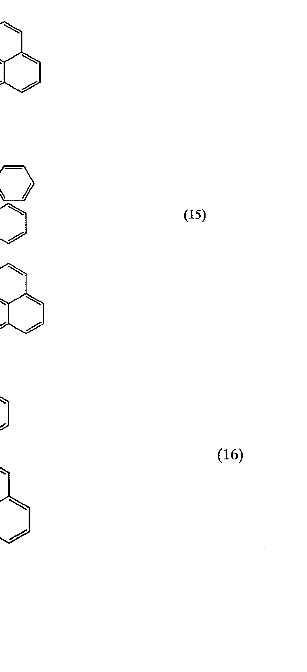
- the reaction mixture was refluxed for 4 hours. Thereafter, the reaction mixture is poured into a large amount of diluted hydrochloric acid. The precipitated solid was collected by filtration. The filtrate was washed with ethanol followed by hexane. The obtained solid was dissolved in hot ethyl acetate, and the insoluble matter was separated by filtration. The obtained solution was concentrated and then left at room temperature to perform a recrystallization operation. The precipitated crystals were collected by filtration and dried under reduced pressure to obtain the compound represented by the structural formula (16), 1 (4′-methyl-1naphthyl) pyrene, in a yield of 67%. The compound was measured by NMR to find that J H NMR (300MHZ, CDCl) ⁇ 7.20-8.30 (m, 15H)
- FIG. 2 shows a voltage-luminance curve of this device.
- Light emission started at around 4 V and was 3600 cdZm 2 when 10 V was applied.
- Fig. 3 shows the emission spectrum. The emission maximum is at 450 nm, confirming that it emits blue light.
- the X value is 0.17 and the y value is 0.23, which indicates that the blue light emission is good.
- Copper phthalocyanine as a hole injection material and NPB as a hole transport material were sequentially formed on the ITO film formed on the glass substrate by a vacuum evaporation method.
- the film thicknesses are 2 Onm and 30 nm, respectively.
- a compound represented by the structural formula (16) was deposited on this laminated film to a thickness of 30 nm, and Alq, an electron transporting material, was laminated to a thickness of 20 nm.
- An electron injection material, CaF was formed thereon, and an A1 electrode was further formed.
- FIG. 4 shows a voltage-luminance curve of this device. Luminescence starts around 5V and applies 10V As a result, a light emission of 9000 cdZm 2 was obtained.
- Fig. 5 shows the emission spectrum. The emission color is blue, the emission maximum is at 450 nm, and it can be confirmed that the emission is blue. As the CIE chromaticity coordinates, both the X value and the y value are about 0.15, which indicates that the blue light emission is good.
- FIG. 6A is a top view illustrating the light-emitting device
- FIG. 6B is a cross-sectional view of FIG. 6A cut along AA ′.
- Reference numeral 401 indicated by a dotted line denotes a driving circuit unit (source-side driving circuit)
- 402 denotes a pixel unit
- 403 denotes a driving circuit unit (gate-side driving circuit).
- Reference numeral 404 denotes a sealing substrate
- 405 denotes a sealing material
- an inside surrounded by the sealing material 405 is a space 407.
- a wiring 408 for transmitting signals input to the source-side driving circuit 401 and the gate-side driving circuit 403 is provided from an FPC (flexible printed circuit) 409 serving as an external input terminal to a video signal, a clock signal, A start signal, a reset signal, and the like are received.
- FPC flexible printed circuit
- PWB printed wiring board
- source-side drive circuit 401 which is a drive circuit portion and pixel portion 402 are shown.
- the source-side drive circuit 401 is a CMOS circuit formed by combining an n-channel TFT 423 and a p-channel TFT 424.
- the TFT forming the driver circuit may be formed using a known CMOS circuit, PMOS circuit, or NMOS circuit.
- a driver integrated with a driver circuit formed over a substrate is shown; however, a driver circuit which does not always need to have such a structure can be formed outside the substrate rather than on the substrate.
- the pixel portion 402 is formed by a plurality of pixels including a switching TFT 411, a current control TFT 412, and a first electrode 413 that is electrically connected to the drain.
- an insulator 414 is formed to cover an end of the first electrode 413.
- it is formed by using a positive photosensitive acrylic resin film.
- a curved surface having a curvature is formed at the upper end or the lower end of the insulator 414.
- a positive photosensitive acrylic is used as the material of the insulator 414, it is preferable that only the upper end portion of the insulator 414 has a curved surface having a radius of curvature (0.3 ⁇ m).
- the insulator 414 either a negative type which becomes insoluble in an etchant by photosensitive light or a positive type which becomes soluble in an etchant by light can be used.
- a layer 416 containing a light-emitting substance and a second electrode 417 are formed over the first electrode 413, respectively.
- a material used for the first electrode 413 functioning as an anode a material having a high work function is preferably used.
- a single-layer film such as an ITO (indium tin oxide) film, an indium zinc oxide film (IZO) film, a titanium nitride film, a chromium film, a tungsten film, a Zn film, a Pt film, etc.
- a three-layer structure of a titanium nitride film, a film mainly containing aluminum, and a titanium nitride film, or the like Note that with a stacked structure, a good ohmic contact having low resistance as a wiring can be obtained, and further, it can function as an anode.
- the layer 416 containing a light-emitting substance is formed by an evaporation method using an evaporation mask or an inkjet method.
- the light-emitting organic compound of the present invention is partly used for the layer 416 containing a light-emitting substance.
- a material that can be used for the layer 416 containing a light-emitting substance may be a low-molecular material or a high-molecular material.
- an organic compound is usually used in a single layer or a stacked layer in many cases; however, in this embodiment, a part of a film including an organic compound is used as an inorganic compound. A configuration using a product is also included.
- a layer containing the organic compound of the present invention as a luminescent substance was formed for each of different luminescent colors by using a mask or a partition layer. They may be formed separately. In this case, a different layered structure may be provided for each layer containing a light-emitting substance that emits each color.
- the second electrode (cathode) 417 formed on the layer 416 containing a light-emitting substance a material having a small work function (Al, Ag, Li, Ca, or an alloy thereof MgAg , Mgln, A1-Li, CaF, or CaN).
- a layer containing a light-emitting substance 416 In order to allow the light generated by the light to pass through the second electrode 417, the second electrode (cathode) 417 may be used as a thin metal film and a transparent conductive film (ITO (indium stannate oxide)). Lamination), indium oxide, zinc oxide (ZnO), zinc oxide (ZnO), etc.)
- the sealing substrate 404 by attaching the sealing substrate 404 to the element substrate 410 with the sealing material 405, the light emitting element 418 is provided in the space 407 surrounded by the element substrate 410, the sealing substrate 404, and the sealing material 405. It has a structure. Note that the space 407 is filled with an inert gas (nitrogen, argon, or the like) as well as a structure filled with a sealant 405.
- an inert gas nitrogen, argon, or the like
- an epoxy resin for the sealant 405 it is preferable to use an epoxy resin for the sealant 405! In addition, it is desirable that these materials are materials that do not transmit moisture and oxygen as much as possible.
- a material used for the sealing substrate 404 a glass substrate, a quartz substrate, or a plastic substrate made of a material such as FRP (Fiberglass-Reinforced Plastics), PVF (polyvinyl fluoride), mylar, polyester, or acrylic may be used. it can.
- the life can be prolonged.
- an electronic device to which the present invention is applied will be described with reference to FIG.
- the present invention for example, in an electronic device as described below, even when used for a long time, a good display image in which defects due to the life of the light emitting element are suppressed can be obtained.
- FIG. 7A shows a display device, which includes a housing 5501, a support base 5502, and a display portion 5503.
- the display device can be completed by incorporating the light-emitting device described in Embodiment 4 into the display device.
- FIG. 7B shows a video camera, which includes a main body 5511, a display portion 5512, an audio input 5513, an operation switch 5514, a battery 5515, an image receiving portion 5516, and the like.
- the display device can be completed by incorporating the light emitting device described in Embodiment 4 into a video camera.
- FIG. 7C shows a notebook personal computer manufactured by applying the present invention, which is composed of a main body 5521, a window 5522, a display 5552, a keyboard 5524, and the like. .
- a notebook personal computer manufactured by applying the present invention which is composed of a main body 5521, a window 5522, a display 5552, a keyboard 5524, and the like.
- FIG. 7D shows a personal digital assistant (PDA) manufactured by applying the present invention, in which a main body 5531 is provided with a display portion 5533, an external interface 5535, operation buttons 5534, and the like. . There is a stylus 5532 as an accessory for operation.
- a display device can be completed by incorporating the light emitting device described in Embodiment 4 into a personal digital assistant (PDA).
- FIG. 7E shows a digital camera, which is composed of a main body 5551, a display section (A) 5552, an eyepiece section 5553, an operation switch 5554, a display section (B) 5555, a nottery 5556, and the like.
- the display device can be completed by incorporating the light emitting device described in Embodiment 4 into a digital video camera.
- FIG. 7F shows a mobile phone manufactured by applying the present invention.
- the main body 5561 is provided with a display portion 5564, an audio output 5562, a microphone 5563, an operation switch 5565, an antenna 5566, and the like.
- the display device can be completed by incorporating the light emitting device described in Embodiment 4 into a mobile phone.
- the light emitting device obtained by implementing the present invention may be used as a display unit of any electronic device.
Landscapes
- Chemical & Material Sciences (AREA)
- Engineering & Computer Science (AREA)
- Materials Engineering (AREA)
- Physics & Mathematics (AREA)
- Spectroscopy & Molecular Physics (AREA)
- Organic Chemistry (AREA)
- Electroluminescent Light Sources (AREA)
- Organic Low-Molecular-Weight Compounds And Preparation Thereof (AREA)
Abstract
Description




Claims


Priority Applications (1)
| Application Number | Priority Date | Filing Date | Title |
|---|---|---|---|
| JP2005512004A JP4737678B2 (ja) | 2003-07-28 | 2004-07-15 | 発光性有機化合物およびそれを用いた発光素子 |
Applications Claiming Priority (2)
| Application Number | Priority Date | Filing Date | Title |
|---|---|---|---|
| JP2003280687 | 2003-07-28 | ||
| JP2003-280687 | 2003-07-28 |
Publications (1)
| Publication Number | Publication Date |
|---|---|
| WO2005010012A1 true WO2005010012A1 (ja) | 2005-02-03 |
Family
ID=34100886
Family Applications (1)
| Application Number | Title | Priority Date | Filing Date |
|---|---|---|---|
| PCT/JP2004/010104 Ceased WO2005010012A1 (ja) | 2003-07-28 | 2004-07-15 | 発光性有機化合物およびそれを用いた発光素子 |
Country Status (3)
| Country | Link |
|---|---|
| US (1) | US7541098B2 (ja) |
| JP (1) | JP4737678B2 (ja) |
| WO (1) | WO2005010012A1 (ja) |
Cited By (6)
| Publication number | Priority date | Publication date | Assignee | Title |
|---|---|---|---|---|
| JP2006269670A (ja) * | 2005-03-23 | 2006-10-05 | Fuji Photo Film Co Ltd | 有機el素子及び有機elディスプレイ |
| WO2007129702A1 (ja) * | 2006-05-09 | 2007-11-15 | Idemitsu Kosan Co., Ltd. | ケイ素含有化合物及びそれを利用した有機エレクトロルミネッセンス素子 |
| JP2009179627A (ja) * | 2007-12-31 | 2009-08-13 | Gracel Display Inc | 有機エレクトロルミネセント化合物及びこれを使用する発光ダイオード |
| JP2010021561A (ja) * | 2004-02-09 | 2010-01-28 | Lg Display Co Ltd | 有機エレクトロルミネセンス素子に使用する新規青色発光体 |
| JP2010527995A (ja) * | 2007-05-21 | 2010-08-19 | グラセル・ディスプレイ・インコーポレーテッド | 有機電界発光化合物及びこれを使用している有機発光ダイオード |
| JP2016524624A (ja) * | 2013-06-07 | 2016-08-18 | オブシェストヴォ ス オグラニチェンノイ オトヴェトストヴェンノスチユ “リュミネスツェントヌィエ インノヴァツィオンヌィエ テフノロギー” | 新規な分岐オリゴアリールシラン及びその調製法 |
Families Citing this family (12)
| Publication number | Priority date | Publication date | Assignee | Title |
|---|---|---|---|---|
| US7233019B2 (en) * | 2004-04-26 | 2007-06-19 | E. I. Du Pont De Nemours And Company | Electroluminescent silylated pyrenes, and devices made with such compounds |
| WO2007065550A1 (de) * | 2005-12-08 | 2007-06-14 | Merck Patent Gmbh | Neue materialien für organische elektrolumineszenzvorrichtungen |
| KR101084100B1 (ko) | 2006-06-01 | 2011-11-16 | 가부시키가이샤 한도오따이 에네루기 켄큐쇼 | 발광소자 |
| US9397308B2 (en) * | 2006-12-04 | 2016-07-19 | Semiconductor Energy Laboratory Co., Ltd. | Light emitting element, light emitting device, and electronic device |
| JP5352304B2 (ja) * | 2008-04-02 | 2013-11-27 | 株式会社半導体エネルギー研究所 | アントラセン誘導体、発光材料、発光素子用材料、塗布用組成物、発光素子、及び発光装置 |
| EP2112212B1 (en) | 2008-04-24 | 2013-05-29 | Semiconductor Energy Laboratory Co., Ltd. | Anthracene derivative, light-emitting material, material for light-emitting element, composition for coating light-emitting element, light-emitting device, and electronic device |
| JP5501656B2 (ja) | 2008-05-16 | 2014-05-28 | 株式会社半導体エネルギー研究所 | 組成物、薄膜の作製方法、及び発光素子の作製方法 |
| US20100156957A1 (en) * | 2008-12-19 | 2010-06-24 | Semiconductor Energy Laboratory Co., Ltd. | Organic compound, anthracene derivative, and light-emitting elements, light-emitting devices, electronic devices, and lighting devices using the anthracene derivative |
| US20100244677A1 (en) * | 2009-03-31 | 2010-09-30 | Begley William J | Oled device containing a silyl-fluoranthene derivative |
| US8283855B2 (en) * | 2010-01-11 | 2012-10-09 | Semiconductor Energy Laboratory Co., Ltd. | Method for synthesis of anthracene derivative |
| US8778223B2 (en) | 2011-05-24 | 2014-07-15 | Lc Vision, Llc | Liquid crystals having cyclohexyl core structures and fluorinated tails |
| DE112015007286B4 (de) | 2014-08-08 | 2025-11-20 | Semiconductor Energy Laboratory Co., Ltd. | Licht emittierende Vorrichtung |
Citations (4)
| Publication number | Priority date | Publication date | Assignee | Title |
|---|---|---|---|---|
| JP2000021575A (ja) * | 1998-04-30 | 2000-01-21 | Fuji Photo Film Co Ltd | 特定のビニルシラン化合物およびそれを含有する有機発光素子、および、ビニルシラン化合物の製造方法。 |
| JP2000143558A (ja) * | 1998-11-12 | 2000-05-23 | Samsung Sdi Co Ltd | 発光化合物及びこれを発色材料として採用している表示素子 |
| JP2000239291A (ja) * | 1998-12-22 | 2000-09-05 | Mitsubishi Chemicals Corp | 金属錯体化合物およびそれを用いた有機電界発光素子 |
| JP2000351966A (ja) * | 1999-04-07 | 2000-12-19 | Fuji Photo Film Co Ltd | 特定のシラン化合物及びそれらからなる発光素子材料、及び、それを含有する発光素子。 |
Family Cites Families (8)
| Publication number | Priority date | Publication date | Assignee | Title |
|---|---|---|---|---|
| US3465017A (en) * | 1967-04-24 | 1969-09-02 | Us Air Force | Preparation of triphenyl (biphenylyl) silanes |
| JP4512217B2 (ja) * | 1999-08-20 | 2010-07-28 | 富士フイルム株式会社 | アリールシラン化合物、発光素子材料およびそれを使用した発光素子 |
| KR100377575B1 (ko) * | 2000-10-17 | 2003-03-26 | 삼성에스디아이 주식회사 | 유기 전계 발광 소자용 청색 발광 화합물 및 이를 사용한유기 전계 발광 소자 |
| JP3870102B2 (ja) * | 2001-02-22 | 2007-01-17 | キヤノン株式会社 | 有機発光素子 |
| JP4003824B2 (ja) * | 2001-07-11 | 2007-11-07 | 富士フイルム株式会社 | 発光素子 |
| JP4871464B2 (ja) * | 2001-09-28 | 2012-02-08 | キヤノン株式会社 | 有機発光素子 |
| TWI314947B (en) * | 2002-04-24 | 2009-09-21 | Eastman Kodak Compan | Organic light emitting diode devices with improved operational stability |
| US20040126617A1 (en) * | 2002-12-31 | 2004-07-01 | Eastman Kodak Company | Efficient electroluminescent device |
-
2004
- 2004-07-15 WO PCT/JP2004/010104 patent/WO2005010012A1/ja not_active Ceased
- 2004-07-15 JP JP2005512004A patent/JP4737678B2/ja not_active Expired - Fee Related
- 2004-07-26 US US10/898,625 patent/US7541098B2/en not_active Expired - Fee Related
Patent Citations (4)
| Publication number | Priority date | Publication date | Assignee | Title |
|---|---|---|---|---|
| JP2000021575A (ja) * | 1998-04-30 | 2000-01-21 | Fuji Photo Film Co Ltd | 特定のビニルシラン化合物およびそれを含有する有機発光素子、および、ビニルシラン化合物の製造方法。 |
| JP2000143558A (ja) * | 1998-11-12 | 2000-05-23 | Samsung Sdi Co Ltd | 発光化合物及びこれを発色材料として採用している表示素子 |
| JP2000239291A (ja) * | 1998-12-22 | 2000-09-05 | Mitsubishi Chemicals Corp | 金属錯体化合物およびそれを用いた有機電界発光素子 |
| JP2000351966A (ja) * | 1999-04-07 | 2000-12-19 | Fuji Photo Film Co Ltd | 特定のシラン化合物及びそれらからなる発光素子材料、及び、それを含有する発光素子。 |
Cited By (6)
| Publication number | Priority date | Publication date | Assignee | Title |
|---|---|---|---|---|
| JP2010021561A (ja) * | 2004-02-09 | 2010-01-28 | Lg Display Co Ltd | 有機エレクトロルミネセンス素子に使用する新規青色発光体 |
| JP2006269670A (ja) * | 2005-03-23 | 2006-10-05 | Fuji Photo Film Co Ltd | 有機el素子及び有機elディスプレイ |
| WO2007129702A1 (ja) * | 2006-05-09 | 2007-11-15 | Idemitsu Kosan Co., Ltd. | ケイ素含有化合物及びそれを利用した有機エレクトロルミネッセンス素子 |
| JP2010527995A (ja) * | 2007-05-21 | 2010-08-19 | グラセル・ディスプレイ・インコーポレーテッド | 有機電界発光化合物及びこれを使用している有機発光ダイオード |
| JP2009179627A (ja) * | 2007-12-31 | 2009-08-13 | Gracel Display Inc | 有機エレクトロルミネセント化合物及びこれを使用する発光ダイオード |
| JP2016524624A (ja) * | 2013-06-07 | 2016-08-18 | オブシェストヴォ ス オグラニチェンノイ オトヴェトストヴェンノスチユ “リュミネスツェントヌィエ インノヴァツィオンヌィエ テフノロギー” | 新規な分岐オリゴアリールシラン及びその調製法 |
Also Published As
| Publication number | Publication date |
|---|---|
| US20050095455A1 (en) | 2005-05-05 |
| JPWO2005010012A1 (ja) | 2006-09-28 |
| JP4737678B2 (ja) | 2011-08-03 |
| US7541098B2 (en) | 2009-06-02 |
Similar Documents
| Publication | Publication Date | Title |
|---|---|---|
| JP4129558B2 (ja) | 有機elディスプレイ | |
| TWI483920B (zh) | 螺茀衍生物,用於發光元件之材料,發光元件,發光裝置,及電子裝置 | |
| JP4737678B2 (ja) | 発光性有機化合物およびそれを用いた発光素子 | |
| KR101254278B1 (ko) | 퀴녹살린 유도체를 이용한 트랜지스터 | |
| JP3965063B2 (ja) | 有機エレクトロルミネッセンス素子 | |
| TWI363084B (en) | Quinoxaline derivatives, and light emitting element using thereof | |
| JP4974509B2 (ja) | 発光素子及び発光装置 | |
| US7977865B2 (en) | Composite material, material for light-emitting element, light-emitting element, light-emitting device and electronic device | |
| WO2004081019A1 (ja) | 有機金属錯体、前記錯体を用いた電界発光材料および前記錯体を用いた電界発光素子 | |
| WO2004046275A1 (ja) | 電界発光素子および発光装置 | |
| WO2005002288A1 (ja) | 共役分子及びそれを用いた電界発光素子、並びに電界発光素子を用いた電子機器 | |
| EP1652902B1 (en) | Oligonaphthalene derivatives, and light-emitting element and light-emitting device using oligonaphthalene derivatives | |
| US7737235B2 (en) | Vinyl monomer and polymer derived from the monomer, and light emitting device using the polymer | |
| JP4683882B2 (ja) | ピラン誘導体とその製造方法、並びにピラン誘導体を用いた発光素子及び発光装置。 | |
| US7364804B2 (en) | Pyran derivative, method for manufacturing the same, and light-emitting element containing the pyran derivative |
Legal Events
| Date | Code | Title | Description |
|---|---|---|---|
| WWE | Wipo information: entry into national phase |
Ref document number: 2005512004 Country of ref document: JP |
|
| AK | Designated states |
Kind code of ref document: A1 Designated state(s): AE AG AL AM AT AU AZ BA BB BG BR BW BY BZ CA CH CN CO CR CU CZ DE DK DM DZ EC EE EG ES FI GB GD GE GH GM HR HU ID IL IN IS JP KE KG KP KR KZ LC LK LR LS LT LU LV MA MD MG MK MN MW MX MZ NA NI NO NZ OM PG PH PL PT RO RU SC SD SE SG SK SL SY TJ TM TN TR TT TZ UA UG US UZ VC VN YU ZA ZM ZW |
|
| AL | Designated countries for regional patents |
Kind code of ref document: A1 Designated state(s): BW GH GM KE LS MW MZ NA SD SL SZ TZ UG ZM ZW AM AZ BY KG KZ MD RU TJ TM AT BE BG CH CY CZ DE DK EE ES FI FR GB GR HU IE IT LU MC NL PL PT RO SE SI SK TR BF BJ CF CG CI CM GA GN GQ GW ML MR NE SN TD TG |
|
| 121 | Ep: the epo has been informed by wipo that ep was designated in this application | ||
| 122 | Ep: pct application non-entry in european phase |