WO2004068564A1 - 照明光学系、照明装置、投影露光装置、及び露光方法 - Google Patents

照明光学系、照明装置、投影露光装置、及び露光方法 Download PDF

Info

Publication number
WO2004068564A1
WO2004068564A1 PCT/JP2003/017043 JP0317043W WO2004068564A1 WO 2004068564 A1 WO2004068564 A1 WO 2004068564A1 JP 0317043 W JP0317043 W JP 0317043W WO 2004068564 A1 WO2004068564 A1 WO 2004068564A1
Authority
WO
WIPO (PCT)
Prior art keywords
mirror
optical system
illumination optical
light
array
Prior art date
Legal status (The legal status is an assumption and is not a legal conclusion. Google has not performed a legal analysis and makes no representation as to the accuracy of the status listed.)
Ceased
Application number
PCT/JP2003/017043
Other languages
English (en)
French (fr)
Inventor
Kenji Suzuki
Kiyoshi Mitarai
Current Assignee (The listed assignees may be inaccurate. Google has not performed a legal analysis and makes no representation or warranty as to the accuracy of the list.)
Nikon Corp
Original Assignee
Nikon Corp
Priority date (The priority date is an assumption and is not a legal conclusion. Google has not performed a legal analysis and makes no representation as to the accuracy of the date listed.)
Filing date
Publication date
Application filed by Nikon Corp filed Critical Nikon Corp
Priority to AU2003296167A priority Critical patent/AU2003296167A1/en
Priority to JP2005515525A priority patent/JPWO2004068564A1/ja
Publication of WO2004068564A1 publication Critical patent/WO2004068564A1/ja
Anticipated expiration legal-status Critical
Ceased legal-status Critical Current

Links

Classifications

    • G—PHYSICS
    • G03—PHOTOGRAPHY; CINEMATOGRAPHY; ANALOGOUS TECHNIQUES USING WAVES OTHER THAN OPTICAL WAVES; ELECTROGRAPHY; HOLOGRAPHY
    • G03F—PHOTOMECHANICAL PRODUCTION OF TEXTURED OR PATTERNED SURFACES, e.g. FOR PRINTING, FOR PROCESSING OF SEMICONDUCTOR DEVICES; MATERIALS THEREFOR; ORIGINALS THEREFOR; APPARATUS SPECIALLY ADAPTED THEREFOR
    • G03F7/00—Photomechanical, e.g. photolithographic, production of textured or patterned surfaces, e.g. printing surfaces; Materials therefor, e.g. comprising photoresists; Apparatus specially adapted therefor
    • G03F7/70—Microphotolithographic exposure; Apparatus therefor
    • G03F7/70058—Mask illumination systems
    • G—PHYSICS
    • G21—NUCLEAR PHYSICS; NUCLEAR ENGINEERING
    • G21K—HANDLING OF PARTICLES OR IONISING RADIATION NOT OTHERWISE PROVIDED FOR; IRRADIATION DEVICES; GAMMA RAY OR X-RAY MICROSCOPES
    • G21K1/00—Arrangements for handling particles or ionising radiation, e.g. focusing or moderating
    • G21K1/06—Arrangements for handling particles or ionising radiation, e.g. focusing or moderating using diffraction, refraction or reflection, e.g. monochromators

Definitions

  • Illumination optical system illumination device, projection exposure apparatus, and exposure method
  • the present invention relates to an illumination optical system and an illumination device mounted on a projection exposure apparatus, and more particularly, to an illumination optical system and an illumination device suitable for extreme ultraviolet light (Extreme Ultra Violet light: hereinafter referred to as EUV light).
  • EUV light extreme ultraviolet light
  • the present invention also relates to a projection exposure apparatus using the illumination optical system and the illumination device.
  • the present invention relates to an exposure method for manufacturing good microdevices (semiconductor devices, imaging devices, liquid crystal display devices, thin-film magnetic heads, etc.) using these illumination optical systems and illumination devices.
  • Background art is an exposure method for manufacturing good microdevices (semiconductor devices, imaging devices, liquid crystal display devices, thin-film magnetic heads, etc.) using these illumination optical systems and illumination devices.
  • the exposure wavelength tends to be shortened in order to improve the integration density of semiconductors.
  • the mercury i-line (wavelength 365. 0 1 5 nm), r F excimer laser (wavelength 248 nm), A r F excimer laser (wavelength 1 93 nm), F 2 excimer laser (wavelength 157 nm).
  • EUV light particularly EUV light with a wavelength of 50 nm or less, as a light source is also being studied.
  • EUV light having a wavelength of 50 nm or less is used, it is necessary to configure the optical system as a reflection type (for example, an illumination optical system described in JP-A-2000-349009).
  • EUV light particularly EUV light having a wavelength of 50 nm or less, cannot be reflected with a sufficient reflectance, so that a large amount of light is lost. .
  • an object of the present invention is to provide an illumination optical system and an illumination device with small light amount loss even when EUV light is used as a light source.
  • Another object of the present invention is to provide a high-performance projection exposure apparatus using the above-mentioned illumination optical system and illumination apparatus.
  • the present invention provides an exposure method capable of manufacturing a microdevice (semiconductor device, image pickup device, liquid crystal display device, thin-film magnetic head, etc.) which is excellent by using the above-mentioned illumination optical system and illumination device. With the goal.
  • the illumination optical system includes a light source unit that emits extreme ultraviolet light, a collimator mirror, a fly-eye mirror, and a condenser mirror, which are sequentially arranged.
  • Each of the collimator mirror, fly-eye mirror, and condenser mirror is configured to detect incident light. It is characterized by comprising a plurality of unit mirrors arranged in such a posture that the oblique incidence angle becomes the total reflection angle.
  • the light source unit is disposed in the vicinity of a laser plasma light source, a collector mirror that collects extreme ultraviolet light emitted from the laser plasma light source, and a collection point of the extreme ultraviolet light by the collector mirror. And a partition for blocking flying objects.
  • the light source unit includes a discharge plasma light source.
  • the light source unit comprises: a collector mirror that collects extreme ultraviolet light emitted from the discharge plasma light source; and a scattered object disposed near the extreme ultraviolet light collection point by the collector mirror. And a partition wall.
  • the collector mirror is composed of a plurality of unit mirrors arranged so that the oblique incident angle of the incident light becomes the total reflection angle.
  • the collimator mirror is configured such that a plurality of skirt-shaped unit mirrors having different diameters and divergent angles are arranged around the optical axis with their divergent portions facing the emission side.
  • the reflecting surfaces of the plurality of skirt-shaped unit mirrors have a shape of a partial side surface of a cone.
  • the unit mirror arranged on the outermost peripheral side of the unit mirror One reflecting surface has a parabolic shape
  • the other reflecting surface of the unit mirror has a shape of a partial side surface of a cone.
  • a cabinary array having a plurality of hollow tubes arranged in parallel is arranged between the collimator mirror and the fly-eye mirror.
  • a cooling mechanism for cooling the above-mentioned capillary array is provided.
  • the fly-eye mirror comprises: an input end in which a plurality of unit mirrors having the same posture are arranged in parallel; and an emission end in which a plurality of unit mirrors having the same posture are arranged in parallel.
  • the oblique incident angle of the incident light becomes the total reflection angle, they are arranged at a sufficient interval in the traveling direction of the reflected light by the unit mirrors.
  • the reflecting surfaces of the plurality of unit mirrors disposed at the incident end each have an Alter I shape.
  • the reflection surfaces of the plurality of unit mirrors disposed at the entrance end and the exit end each have a parabolic shape.
  • the plurality of unit mirrors constituting the incident end are arranged by being shifted by a sufficient distance in a traveling direction of the reflected light by the unit mirrors so as to reduce vignetting of the reflected light between the unit mirrors.
  • the plurality of unit mirrors constituting the emission end are arranged by being shifted by a sufficient distance in the traveling direction of the reflected light by the unit mirrors so that the vignetting of the reflected light between the unit mirrors is reduced.
  • the condenser mirror has a plurality of unit mirrors arranged in series, and at least one of the reflection surfaces is a toroidal aspheric surface. More preferably, the extreme ultraviolet light emitted from the light source unit is an extreme ultraviolet light having a wavelength of 50 nm or less, and the reflecting surfaces of the unit mirrors of the collimator mirror, the fly-eye mirror, and the condenser mirror are each composed of Ru. Or, it is made of a material of Mo, and is arranged in such a posture that the oblique incident angle is 15 ° or less.
  • a projection exposure apparatus includes a reflective projection optical system and any one of the illumination optical systems according to the present invention.
  • the exposure method of the present invention illuminates a reticle using any of the illumination optical systems of the present invention. And an exposure step of exposing the reticle pattern to a photosensitive substrate.
  • a lighting device includes a light source unit that supplies extreme ultraviolet light, and an illumination optical system that guides light from the light source unit to an object to be illuminated.
  • the illumination optical system includes a plurality of light sources that reflect the extreme ultraviolet light. Wherein all of the reflecting members constituting the illumination optical system are arranged in a posture in which the incident angle of incident light is the total reflection angle.
  • the plurality of reflecting members include at least an array-shaped mirror having a large number of reflecting elements, and the large number of reflecting elements in the arrayed mirror are arranged in a posture in which an incident angle of incident light is a total reflection angle.
  • the multiple reflecting elements in the array mirror have predetermined optical powers in the meridional direction and the sagittal direction, respectively.
  • the plurality of reflecting members include at least a first array mirror having a plurality of first reflecting elements, and a second array mirror having a plurality of second reflecting elements.
  • a large number of first reflecting elements in the one array-shaped mirror and a large number of second reflecting elements in the second array-shaped mirror are respectively arranged in such a manner that the incident angle of incident light becomes the total reflection angle. .
  • the illumination device of the present invention includes a light source unit that supplies extreme ultraviolet light, and an illumination optical system that guides light from the light source unit to an object to be illuminated, and the illumination optical system reflects the extreme ultraviolet light.
  • a plurality of reflecting members, the plurality of reflecting members comprising: a first array-shaped mirror having a large number of first reflecting elements; and a second array-shaped mirror having a large number of second reflecting elements.
  • the multiple first reflecting elements in the first array mirror and the multiple second reflecting elements in the second array mirror have a posture in which an incident angle of incident light is a total reflection angle. It is characterized by being arranged respectively.
  • the multiple first reflecting elements in the first array-shaped mirror and the multiple second reflecting elements in the second array-shaped mirror have a predetermined optical power in the meridional direction and the sagittal direction. .
  • the light passing through the first array mirror and the second array mirror is the second array mirror, the vicinity of the second array mirror, Alternatively, a number of converging points as secondary light sources are formed on the exit side of the second array mirror.
  • At least one of the first reflection element and the second reflection element includes a parabolic reflection surface.
  • the plurality of first reflecting elements in the first array-shaped mirror are arranged on a first reference plane inclined at a predetermined angle with respect to an incident optical path incident on the first array-shaped mirror.
  • a large number of the second reflecting elements in the second array mirror are densely arranged on a second reference plane inclined at a predetermined angle to an incident optical path incident on the second array mirror. It is characterized by being arranged.
  • the plurality of first reflecting elements in the first array-shaped mirror are inclined at a predetermined angle ⁇ 1 with respect to the central light of light incident on each of the plurality of first reflecting elements.
  • the plurality of second reflecting elements in the second array-shaped mirror are densely arranged on the first reference plane, and are predetermined with respect to the center light of light incident on each of the plurality of first reflecting elements.
  • Angle] 3 2 are densely arranged on a second reference plane inclined at 2 2, and the predetermined angle 1 and the predetermined angle 2 are 0 ° ⁇ 3 1 ⁇ 20 °, 0 ° ⁇ 2
  • the projection exposure apparatus of the present invention includes any one of the illuminating apparatuses of the present invention, and a projection optical system that projects a reticle pattern as the illuminated object illuminated by the illuminating apparatus onto a photosensitive substrate. I do.
  • the exposure method of the present invention includes an illuminating step of illuminating a reticle as the object to be illuminated using any one of the illuminating apparatuses of the present invention, and an exposing step of exposing a pattern of the reticle to a photosensitive substrate. It is characterized by the following.
  • the exposure method of the present invention includes a step of supplying extreme ultraviolet light, a step of illuminating a reticle with the extreme ultraviolet light, and a step of exposing a pattern of the reticle to a photosensitive substrate.
  • the exposure method of the present invention includes a step of supplying extreme ultraviolet light, a step of illuminating a reticle with the extreme ultraviolet light, and a step of exposing a pattern of the reticle to a photosensitive substrate.
  • the first array-shaped mirror having a number of first reflection elements arranged in a posture where the incident angle of the incident light is the total reflection angle; and the incident angle of the incident light is the total reflection angle. Guiding the extreme ultraviolet light to the object to be illuminated by using a second array mirror having a plurality of second reflective elements arranged in an angled posture.
  • FIG. 1 is a schematic configuration diagram of an illumination optical system according to the first embodiment.
  • FIG. 2 is a graph showing the relationship between the oblique incidence angle and the reflectance of EUV light having a wavelength of 13.5 nm (with respect to Mo).
  • FIG. 3 is a graph showing the relationship between the oblique incidence angle and the reflectance of EUV light having a wavelength of 13.5 nm (with respect to Ru).
  • FIG. 4 is a graph showing the relationship between the oblique incidence angle of EUV light having a wavelength of 13.5 nm and the reflectance (for Mo Si 2 ).
  • FIG. 5 is a diagram illustrating a collimator mirror 12 according to the first embodiment.
  • FIG. 6 is a diagram illustrating a collimator mirror 12 ′ of the first embodiment.
  • FIGS. 7A and 7B are diagrams illustrating the incident end 13 in of the fly-eye mirror 13 of the first embodiment
  • FIG. 7B is a diagram illustrating the exit end 1 of the fly-eye mirror 13 of the first embodiment. It is a figure showing 3 out.
  • FIG. 8 illustrates the shape of the reflecting surfaces of the unit mirrors 13 in-1, 13 in-2,... Arranged at the entrance end 13 in of the fly-eye mirror 13 of the first embodiment. It is a figure.
  • FIG. 9 is a diagram illustrating a collimator mirror 12 ′′ according to the second embodiment.
  • FIG. 10 is a diagram for explaining the capillary array 12B.
  • FIG. 11 shows the unit mirrors 13 3 in 1, 13 3 in—2, 3 ⁇ in the third embodiment arranged at the entrance end 13 in of the fly-eye mirror 13.
  • FIG. 3 is a diagram illustrating the shape of a reflection surface.
  • FIG. 12 shows a unit mirror 13 "in—1, 13” in—2,..., And a unit mirror disposed at the incident end 13 ”in of the fly-eye mirror 13” according to the fourth embodiment. ⁇ ⁇ Unit mirror placed at the output end 1 3 "out 1 3" out_l, 1 3 "out—2, ⁇ It is a figure explaining the shape of a reflective surface.
  • FIG. 13 is a diagram showing a schematic configuration of a light source unit 21 of the fifth embodiment and its periphery.
  • FIG. 14 is a diagram showing a schematic configuration of the light source unit 31 of the sixth embodiment and its periphery.
  • FIG. 15 is a diagram (perspective view) for explaining the collector mirror 31 c according to the sixth embodiment.
  • FIG. 16 is a diagram illustrating an arrangement relationship between unit mirrors of a fly-eye mirror 33 according to the seventh embodiment.
  • FIG. 17 is a configuration diagram of the projection exposure apparatus of the eighth embodiment.
  • FIG. 18 is a cross-sectional view showing the configuration of the collimator mirror 12 of the first embodiment.
  • FIG. 19 is an optical path diagram showing the configuration of the fly-eye mirror 13 of the first embodiment.
  • FIG. 20 is an optical path diagram showing the configuration of the condenser mirror 14 of the first embodiment.
  • FIG. 21 is a diagram illustrating the positional relationship between the respective reflecting surfaces of the collimator mirror 12 ′′ of the second embodiment.
  • Fig. 22 shows the shape of the reflecting surface of the unit mirror 13, in--1, 13, 12, 12, ⁇ , ⁇ located at the entrance end 13 in of the fly-eye mirror 13 'of the third embodiment.
  • FIG. 23 shows unit mirrors 13 "in-1 and 13" in-2 disposed at the entrance end 13 "in and the exit ends 13 and out of the fly-eye mirror 13" of the fourth embodiment. , ⁇ , 1, 13 ”out—1, 13” out—2, ⁇ , '′.
  • FIG. 23 shows unit mirrors 13 "in-1 and 13" in-2 disposed at the entrance end 13 "in and the exit ends 13 and out of the fly-eye mirror 13" of the fourth embodiment. , ⁇ , 1, 13 ”out—1, 13” out—2, ⁇ , '′.
  • FIG. 24 is an optical path diagram of the fly-eye mirror 33 of the fifth embodiment.
  • FIG. 25 is an optical path diagram showing the configuration of the condenser mirror 14 of the fifth embodiment.
  • FIG. 26 is a flowchart of a method for obtaining a semiconductor device as a micro device.
  • FIG. 27 is a flowchart of a method for obtaining a liquid crystal display element as a micro device.
  • FIG. 1 is a schematic configuration diagram of an illumination optical system according to the present embodiment. It should be noted that the reference numerals 12A, 12B, 12C, 13 ', and 13 "in FIG. 1 are components of an embodiment described later and will not be described here.
  • This illumination optical system is mainly applied to a projection exposure apparatus having a reflection type projection optical system, and illuminates a reticle surface R of the projection exposure apparatus with Koehler illumination.
  • the light source unit 11 of this illumination optical system is a light source unit that emits EUV light (hereinafter referred to as EUV light having a wavelength of 50 nm or less).
  • a laser plasma light source using an efficient Xe as a target, a discharge plasma light source, or the like can be applied to the light source unit 11.
  • a discharge plasma light source has a relatively high energy efficiency, and is advantageous in realizing a high throughput.
  • a collimator mirror 12, a fly-eye mirror 13, and a condenser mirror 14 are sequentially arranged on the emission side of the light source unit 11.
  • the collimator mirror 12 has a plurality of unit mirrors 12-1-1, 12-2,... Arranged in parallel with the incident light beam.
  • the fly-eye mirror 13 has an incident end 13 i ⁇ in which a plurality of unit mirrors 13 3 ⁇ ⁇ - 1, 13 ⁇ ⁇ - 2,... Are arranged in parallel, and a plurality of unit mirrors 1 3 out— 1, 1 3 out One, two, three, two, and three 'are provided.
  • the condenser mirror 14 has a plurality of unit mirrors 14-1, 14-2,... Arranged in series with respect to the incident light beam.
  • the parallel arrangement is an arrangement in which partial light beams different from each other among the incident light beams are individually actuated
  • the serial arrangement is an arrangement which acts on the entire incident light beam in order.
  • the attitude of In, the oblique incidence angle (the angle between the EUV light with a wavelength of 50 nm or less) and the reflecting surface is set to be the total reflection angle.
  • total reflection angle The angle of oblique incidence at which incident light is totally reflected is particularly referred to as “total reflection angle”.
  • these unit mirrors 12-1, 12-2, 1 ⁇ 2, 13 in-1, 13 in-2, 1 ⁇ , 13 out-1, 13 out-2, ⁇ 2 ,, 14-1, 14 2, 1, 2 ⁇ ⁇ ⁇ ′ are made of Mo or Ru, respectively.
  • FIGS. 2, 3, and 4 are diagrams showing the relationship between the oblique incidence angle of EUV light having a wavelength of 13.5 nm and the reflectance.
  • FIG. 2 shows the reflectance of Mo
  • FIG. 3 shows the reflectance of Ru
  • FIG. 4 shows the reflectance of MoSi 2 .
  • the reflectance increases as the oblique incidence angle of the incident light decreases.
  • the total reflection angle of Mo is about 15 ° or less
  • the total reflection angle of Ru is about 15 ° or less
  • the total reflection angle of MoSi 2 is about 10 ° or less.
  • the total reflection angle at which the reflectance is 90% or more is about 10 ° or less for Mo, about 8 ° or less for Ru, and about 5 ° or less for MoSi 2 .
  • the total reflection angle when the Mo or Ru material is used is larger than the total reflection angle when the MoSi 2 material is used.
  • the unit mirrors 12-1, 12-2, ⁇ ⁇ ⁇ , 13 in-1, 13-in-2, ⁇ ⁇ ⁇ ⁇ , 13 out-1, 13 out-2, Since the material of Mo or Ru is used for the reflective surface of ⁇ , ⁇ , 14-1, 14-2, and '', the total reflection angle is relatively large, 15 ° or less.
  • each reflecting surface is higher than when other materials are used.
  • Mo Si 2 material may be used for part or all of each reflecting surface.
  • FIG. 5 is a diagram illustrating the collimator mirror 12 of the present embodiment.
  • FIG. 5A is a sectional view of the collimator mirror 12 cut along a plane including the optical axis Z
  • FIG. 5B is a perspective view of the collimator mirror 12.
  • the collimator mirror 12 is composed of a plurality of skirt-shaped unit mirrors 12-1, 1, 2, 2, 2,...
  • the divergent portion is arranged around the optical axis Z with the diverging portion facing the emission side (the number of unit mirrors is 3 in the figure).
  • Each of the unit mirrors 12-1, 12-2, ⁇ ⁇ has a reflective surface inside.
  • the unit mirror that deflects the marginal rays (that is, the unit mirror that is arranged outside with a larger diameter) has a larger spread angle.
  • the reflecting surfaces of the unit mirrors 12-1, 12-2,... Have the shape of a partial side surface of a cone as shown in FIGS. 5 (a) and 5 (b).
  • the collimator mirror 12 composed of such unit mirrors 12-1, 12-2,... Individually converts light beams emitted from the light source unit 11 at mutually different emission angles into parallel light beams.
  • the oblique incident angle 0 (see FIG. 5A) of the incident light with respect to the reflecting surfaces of the unit mirrors 12-1, 12-2,.
  • each must be suppressed to the total reflection angle (here, less than 15 °).
  • the oblique incidence angle of all the incident light on the collimator mirror 12 may not be possible to make the oblique incidence angle of all the incident light on the collimator mirror 12 equal to the total reflection angle (here, 15 ° or less).
  • the oblique incidence angle of the incident light on the unit mirror with a large diameter may be larger than the total reflection angle (here, less than 15 °).
  • the collimator mirror 12 may be deformed as shown in FIG.
  • FIG. 6 is a diagram illustrating the collimator mirror 12 ′.
  • FIG. 6A is a cross-sectional view of the collimator mirror 12 ′ cut along a plane including the optical axis Z
  • FIG. 6B is a perspective view of the collimator mirror 12 ′.
  • the unit mirror 12-1 arranged on the outermost periphery of the collimator mirror 1 2 ' has a plurality of unit mirrors 12-1-1, 12-1-2,. Then, the number of unit mirrors arranged in series was 3.)
  • each of the unit mirrors 1 2— 1— 1, 1 2— 1— 2, 2,... Has the same shape as the unit mirror 1 2—1 of the collimator mirror 12 shown in FIG.
  • the reflecting surface has the shape of a partial side surface of a cone.
  • the incident light is converted into a light beam parallel to the optical axis z and emitted.
  • a plurality of unit mirrors may be arranged in series for each of the unit mirrors 12-2, 12-3,... Other than the outermost periphery (12-2-2-1, 12-1-2). 2—2, 1 2—2—3, 1 2—3—1, 1 2—3—2, 1 2—3—3).
  • the oblique incidence angle of the light is set to be the total reflection angle (here, 15 ° or less).
  • the entrance end 13 in and the exit end 13 out of the fly-eye mirror 13 are arranged at a sufficient interval in the traveling direction of the light reflected by each unit mirror.
  • FIG. 7 is a diagram illustrating the fly-eye mirror 13.
  • FIG. 7A shows the incident end 13 in of the fly-eye mirror 13
  • FIG. 7B shows the exit end 13 out of the fly-eye mirror 13.
  • FIG. 7 (a) is a view from the collimator mirror 12 side
  • FIG. 7 (b) is a view from the condenser mirror 14 side.
  • FIG. 8 is a view for explaining the shape of the reflecting surface of the unit mirrors 13 in 1, 1 3 in -2, 1 ⁇ arranged at the entrance end 13 in of the fly-eye mirror 13.
  • the reflecting surface of the unit mirror 1 3 in— 1, 1 3 i n- 2, ⁇ ⁇ ⁇ is the exit end 1 3 ou Unit mirrors placed at t 1 3 out-1, 1 3 out-2, ⁇ ⁇ ⁇
  • Each has a partial parabolic shape to form secondary light sources on the top without aberration.
  • the outer shape of the reflecting surface of the unit mirror 13 in-1, 1, 3 in-2,... Is similar to the exposure area of the projection exposure apparatus. Here, it is assumed that the exposure area is an arc field.
  • the condenser mirror 14 reflects the luminous flux emitted from the output end 13 out at the unit mirrors 14-1, 14-2, '' in order, and outputs the secondary light source group formed at the output end 13 ou U.
  • the projection is superimposed on the arc field on the reticle plane R.
  • the shape of at least one of the reflecting surfaces of the unit mirrors 14 1, 14-2,... ′ Is a “toroidal aspheric surface” defined by Expression (1) described later.
  • the illumination optical system according to the present embodiment including the light source unit 11, the collimator mirror 12 (or 12 ′), the fly-eye mirror 13, and the condenser mirror 14 described above has each mirror configured by a plurality of unit mirrors.
  • the loss of EUV light amount can be suppressed to a small value.
  • the reticle surface R is illuminated with a sufficient amount of EUV light.
  • the oblique incidence angle with respect to each reflecting surface is positively set to the total reflection angle (here, 15 °), a multilayer film is formed on each of the reflecting surfaces. No need.
  • the reflecting surfaces of the unit mirrors 12-1, 12-2,... Of the collimator mirror 12 have a relatively simple conical partial side surface shape.
  • the partial side surface of the cone not only resembles a partial paraboloid (a part of a paraboloid), which is the ideal shape for converting a diverging light beam into a parallel light beam, but also that partial paraboloid It is a simpler surface.
  • the unit mirrors 12-1, 12-2,... can be made thin while performing the desired functions.
  • the unit mirrors 12 2—1—1, 1 2—1—2, are applied, the unit mirrors 12 2—1—1, 1 2—1—2,.
  • the deflection angle of the light beam assigned to each is smaller than when only one unit mirror is arranged in series (see Fig. 5), so that the oblique incidence angle of the incident light is set to the total reflection angle (here, 15 ° or less) and the loss of light quantity can be reliably suppressed.
  • the oblique incidence angle of each reflection should be reduced by the number of unit mirrors arranged in series (for example, about 6 °, in which case the reflectance is 90% or more). Can be. In this way, it is possible to perform total reflection at a higher reflectance.
  • the postures of the unit mirrors 14-1, 14-2,... are set so that the oblique incidence angle of the incident light with respect to their reflecting surfaces is further reduced (for example, about 6 °. (The reflectivity of the light is 90% or more).
  • FIG. 1, FIG. 9, and FIG. Book The embodiment is an embodiment of an illumination optical system.
  • a collimator mirror 12 is applied in place of the collimator mirror 12 (or 12) shown in Fig. 1, and a cabary array 12B and a cooling device 12C are added. It is in the point that is.
  • FIG. 9 is a diagram illustrating a collimator mirror 12 ′′ of the present embodiment.
  • FIG. 9A is a cross-sectional view of the collimator mirror 12 "cut along a plane including the optical axis Z
  • FIG. 9B is a perspective view of the collimator mirror 12".
  • the collimator mirror 12 has a unit mirror 12A in the form of a skirt having a reflective surface on the inner side on the outer peripheral side of the collimator mirror 12".
  • the shape of the reflecting surface of the unit mirror 12A is a part of the paraboloid (partial paraboloid) having a center line on the optical axis Z and having a focal point at the position of the light source unit 11.
  • Mo or Ru material is also used for the reflection surface of the unit mirror 12A.
  • a material of MoSi 2 is used for the reflection surface.
  • the oblique incidence angle of the incident light (here, EUV light having a wavelength of 50 nm or less) on the reflecting surface of the unit mirror 12A is the total reflection angle (here, 15 ° or less, but when using MoSi 2 ). Case 10 ° or less).
  • FIG. 4 is a diagram illustrating a rally array 1 2B.
  • FIG. 10 (a) is a cross-sectional view of the caster array 12B cut along a plane including the optical axis Z
  • FIG. 10 (b) is a perspective view of the caster array 12B.
  • the cavity array 12B has a plurality of hollow glass tubes 12B_1, 12B-2, ⁇ 'arranged in parallel.
  • the hollow glass tubes 1 2 B_ 1, 1 2 B-2, ⁇ are the same circular shape with the entrance end 12 Bin and the exit end 12 B out of the cavitary array 12 B Bundle Has been.
  • the collimator mirror 12 "of the embodiment shown in FIG. 9 is used to convert light having a high numerical aperture (large divergence angle) into collimated light with high efficiency without causing loss of light quantity.
  • a high numerical aperture reflector (outer unit mirror: 12 A) that reflects light with a high numerical aperture (large divergence angle) and a smaller numerical aperture (large divergence) than the high numerical aperture (large divergence angle) It has a reflector for the non-high numerical aperture (inner unit mirror: 12A-1; 12A-2;
  • the reflecting surface of unit mirror 12A disposed on the outer peripheral side of collimator mirror 12 "has a shape of a partial paraboloid.
  • the parabolic surface has an ideal shape for converting a diverging light beam into a parallel light beam
  • the peripheral light beam (a light beam with a large divergence angle) emitted from the light source unit 11 is formed. It is surely converted into a parallel light beam.
  • the light amount loss of the EUV light can be further reduced.
  • the discharge plasma light source is applied to the light source unit 11 and the collimator mirror 12 "is used in combination, the emitted light beam from the light source unit 11 is efficiently converted into a parallel light beam.
  • the reflecting surface of the unit mirror 12A on the outer periphery of the collimator mirror 12 is formed in a parabolic shape.
  • the present invention is not limited to this shape. Needless to say, it can be constituted by a mirror (mirror in which a parabolic reflecting surface and a hyperboloid reflecting surface are combined).
  • the capillary array 12B since the capillary array 12B is disposed, the non-parallel light beam (in the collimator mirror 12 ") included in the light beam emitted from the collimator mirror 12" ) Is removed. Further, the capillary array 12B also removes flying objects (generated in the light source unit 11) included in the emitted light beam.
  • the illumination optical system of the present embodiment includes a collimator mirror 12 ", a cabary array 12B, and a cooling device 12C. It is also possible to realize an illumination optical system in which the billy array 12B and the cooling device 12C are omitted, and an illumination optical system in which the cooling device 12C is omitted in the illumination optical system of the present embodiment.
  • the illumination optical system of the first embodiment employs the illumination array 12B and the cooling device 12C, and the illumination optical system of the first embodiment employs the illumination array 12B.
  • a system is also feasible.
  • FIG. 1 A third embodiment of the present invention will be described based on FIG. 1 and FIG.
  • This embodiment is an embodiment of an illumination optical system.
  • FIG. 11 shows the reflection surfaces of the unit mirrors 13, in — 1, 13 ′ in — 2,... ′ Disposed at the entrance end 13 ′ in of the fly-eye mirror 13 ′ of the present embodiment. It is a figure explaining a shape.
  • Each of these reflecting surfaces has an Alternator I shape.
  • the shape of Alter I type consists of the first surface, which is a partial paraboloid, and the second surface, which is a partial hyperboloid.
  • the center lines of the paraboloid and the hyperboloid are on the same straight line, and the focal point of the paraboloid coincides with one of the two focal points F 1 and F 2 of the hyperboloid.
  • the first and second surfaces are surfaces formed by partially cutting out each of the paraboloid and the hyperboloid near the intersection of the two.
  • Such unit mirrors 13 and in_i are arranged such that the center line is parallel to the optical axis Z.
  • the light beam condensing position by the unit mirror 13, in-i is the focal point F 2.
  • a unit mirror 1 3 ′ out — i (a unit mirror arranged at the output end 13 ′ out) corresponding to the unit mirror 13 ′ in — i is arranged.
  • the reflecting surfaces of these unit mirrors 13, in-1, 13 'in-2, ⁇ ⁇ ⁇ , 13, out-1, 13, out-2, ⁇ ⁇ ⁇ are also Mo or Ru material is used.
  • a material of MoSi 2 is used for the reflecting surface.
  • the incident light on the reflecting surfaces of these unit mirrors 13, in-1, 13, in-2, ⁇ ⁇ , 13, out-1, 13, out-2, ⁇ are the total reflection angles (here 15 ° or less, but 10 ° or less when using MoSi 2 ).
  • each of the reflection surfaces at the incident ends 13 and in of the fly-eye mirror 13 ′ has the shape of the alternator I, the Absine sine condition is satisfied.
  • the contours of the reflective surfaces can be made to be the exact analog of the exposure area (here arc fields).
  • FIGS. A fourth embodiment of the present invention will be described with reference to FIGS.
  • This embodiment is an embodiment of an illumination optical system.
  • FIG. 12 shows the unit mirrors 13 "in—1, 1 3” in—2, 1 ⁇ 2 ⁇ and the exit end arranged at the entrance end 13 1in of the fly-eye mirror 13 3 of the present embodiment.
  • FIG. 3 is a diagram for explaining the shape of the reflecting surface of the unit mirrors 13 "out-1, 13, 3" out-2,...
  • the reflecting surface of the unit mirror 13 "1 11 _ 1 has a shape of a partial paraboloid.
  • the reflecting surface of the unit mirror 13 "out-i also has the shape of a partial paraboloid.
  • the former paraboloid and the latter paraboloid have the same shape, center line, and focal point F, and match each other. Only the directions of the vertices are opposite to each other. Note that the paraboloids of the former and the latter may be slightly defocused as needed.
  • the reflecting surface of the unit mirror 13 "in-i and the reflecting surface of the unit mirror 13" out-i can be formed by cutting out the two paraboloids, each of which is symmetrical with respect to the focal point F.
  • the unit mirror 13 "in-i and the unit mirror 13" outt-i are arranged in such a manner that the center line is parallel to the optical axis Z.
  • the light beam incident on the unit mirror 13 "i n-i is once collected at the focal point F, and then diverges and incident on the unit mirror 13" out i-i.
  • these unit mirrors 1 3 "in-1, 13" in-2, ..., 13 "out-1, 1 3" out-2, ⁇ . u material is used.
  • a material of MoSi 2 is used for the reflecting surface.
  • the oblique incidence angle of the following EUV light is the total reflection angle (15 ° or less here, but 10 ° or less when using MoSi 2 ).
  • each of the reflection surfaces of the input end 13 "in and the output end 13" out of the fly-eye mirror 13 has a parabolic shape, Abbe's sine condition can be satisfied, and the contours of the reflecting surfaces can be made to be exactly similar to the exposure area (in this case, an arc field).
  • the reflecting surface of these unit mirrors 1 3 "out-1, 1 3" out-2, ⁇ ⁇ ⁇ is lightly damaged.
  • FIG. 13 is a diagram showing a schematic configuration of the light source unit 21 of the present embodiment and the periphery thereof.
  • the air around the illumination optical system including the light source unit 21 is exhausted by the vacuum chamber 21 e, the exhaust pipe 21 f, and the vacuum pump 21 g (each of the above embodiments).
  • the illumination optical system is also evacuated similarly, but the description is omitted.
  • a laser plasma light source that emits EUV light is applied to the light source unit 21 of the present embodiment.
  • a laser light source 21a In the light source section 21, a laser light source 21a, a plasma supply source 21b for supplying plasma to laser light emitted from the laser light source 21a, and laser light and plasma are generated by reaction.
  • a collector mirror (an elliptical mirror in FIG. 1) 21 c for collecting EUV light and a vacuum chamber 21 d are provided.
  • the reflection surface of the collector mirror 21c which is an elliptical mirror, is provided with a multilayer film for improving the EUV light reflectance.
  • the vacuum chamber 21 d houses a laser light source 21 a, a plasma supply source 2 lb, and a collector mirror 21 c inside the vacuum chamber 21 e.
  • One of the side walls of the vacuum chamber 21 d is arranged so as to cross the optical axis near the EUV light converging point by the collector mirror 21 c, and an opening is formed near the converging point on the side wall. Is provided. In the opening, a pinhole plate P whose pinhole center coincides with the optical axis is provided. Therefore, the substantial opening of the vacuum chamber 21 d is the pinhorn.
  • the air in the vacuum chamber 21 d is exhausted by the exhaust pipe 21 f and the vacuum pump 21 g.
  • the air pressure inside the vacuum chamber 21 d is kept lower than the air pressure in other parts of the illumination optical system.
  • the scattered matter is shielded by the above-described shielding part (the part other than the pinhole) of the pinhole plate P.
  • the air pressure inside the vacuum chamber 21 d is lower than the air pressure in other parts. Therefore, the scattered matter does not travel from the pinhole of the pinhole plate P toward the collimator mirror 12, and passes through the exhaust pipe 21 f and the vacuum pump 21 g provided in the vacuum chamber 21 d. Exhausted to
  • the influence of the scattered matter generated in the light source unit 21 on the optical system after the collimator mirror 12 is eliminated.
  • the positional relationship between the pinhole plate P and the focal point in the direction of the optical axis is desirably selected based on experiments and the like so as to remove flying objects most efficiently.
  • the pinhole of the pinhole plate P does not need to be a complete opening, and may be covered with a film made of beryllium or the like as long as it can transmit EUV light.
  • FIGS. A sixth embodiment of the present invention will be described with reference to FIGS.
  • This embodiment is an embodiment of another light source unit applicable to each of the above illumination optical systems. Here, only the differences from the light source unit of the fifth embodiment will be described.
  • FIG. 14 is a diagram showing a schematic configuration of the light source unit 31 of the present embodiment and the periphery thereof.
  • the air around the illumination optical system including the light source 31 is exhausted by the vacuum chamber 21 e, the exhaust pipe 21 f, and the vacuum pump 21 g (the illumination optical systems of the above embodiments). Is also evacuated similarly, but the explanation is omitted.)
  • a discharge plasma light source that emits EUV light is applied to the light source unit 31 of the present embodiment.
  • the light source section 31 includes a discharge plasma light source 31a, a collector mirror 31c for condensing EUV light (divergent light) emitted from the discharge plasma light source 31a, and a vacuum chamber 31. d is provided.
  • the vacuum chamber 31 d houses a discharge plasma light source 31 a and a collector mirror 31 c inside the vacuum chamber 21 e.
  • a pinhole plate (a pinhole plate having a pinhole near the focal point) P similar to that of the vacuum chamber 21 d of the first embodiment is also provided in the vacuum chamber 31 d.
  • the typical opening is the pinhole of the pinhole plate P.
  • the air in the vacuum chamber 31 d is exhausted by the exhaust pipe 21 f and the vacuum pump 21 g.
  • the light source unit 31 of the present embodiment similarly to the light source unit 21 of the fifth embodiment, the influence of flying objects exerted on the optical system after the collimator mirror 12 is eliminated.
  • FIG. 15 is a diagram (perspective view) illustrating the collector mirror 31 c of the present embodiment.
  • the collector mirror 31 c of the present embodiment is similar to the above-described collimator mirror 12 (see FIG. 5) ⁇ like the collimator mirror 12 ′ (see FIG. 6). It consists of multiple unit mirrors, each of which has an oblique incident angle ⁇ suppressed to the total reflection angle.
  • the shape of the reflecting surface of each unit mirror is a predetermined shape required as a collector mirror, such as the shape of a partial reflecting surface of an elliptical mirror or the shape of a partial side surface of a cone, or an approximate shape thereof.
  • the loss of the amount of EUV light can be suppressed to a small level.
  • the collector mirror 21c of the light source unit 21 of the fifth embodiment is plural (oblique incidence angle is suppressed to the total reflection angle). Or a plurality of unit mirrors).
  • the collector mirror 31c of the light source unit 31 of the present embodiment may be an elliptical mirror.
  • the laser plasma light source is suitable elliptic mirror, when the discharge plasma is suitable plurality of mirrors considered al 0
  • FIG. 16 shows an arrangement relationship of each unit mirror of the fly-eye mirror 33 of the present embodiment.
  • the plurality of unit mirrors 3 3 in — 1, 33 i n_2, ⁇ ⁇ ⁇ constituting the entrance end 33 in of the fly-eye mirror 33 are not only in the direction perpendicular to the incident light (XY direction) but also in the incident light. They are also shifted by a sufficient distance in the direction of travel (Z direction).
  • the multiple unit mirrors that make up the exit end 33 out of the fly-eye mirror 33 — 33 out-l, 33 out-2, ⁇ ⁇ ' are also separated by a sufficient distance not only in the XY direction but also in the Z direction. They are staggered.
  • the sufficient distance is a distance such that the amount of vignetting by the other unit mirrors of the reflected light at each unit mirror is reduced (preferably, there is no vignetting). That is, in the fly-eye mirror 33 of the present embodiment, when the entrance end 33 in of the fly-eye mirror 33 is viewed from the side of the collimator mirror 12, each unit mirror 3 3 in—1, 3 3 in ⁇ The overlap between 2, ⁇ ⁇ ⁇ is reduced (preferably 0), and each unit when viewing the output end 3 3 out of the fly-eye mirror 33 from the condenser mirror 14 side The overlap between the mirrors 3 3 out— 1, 3 3 out— 2, ⁇ ⁇ ⁇ is reduced (preferably 0).
  • the fly-eye mirror 33 of the present embodiment According to the fly-eye mirror 33 of the present embodiment described above, the light amount loss is reduced.
  • FIG. 1 is an embodiment of a projection exposure apparatus.
  • FIG. 17 is a configuration diagram of the projection exposure apparatus of the present embodiment.
  • the projection exposure apparatus is a reduction projection type projection exposure apparatus that performs a scanning exposure operation by a step-and-scan method using EUV light (for example, EUV light having a wavelength of 50 nm or less) as an exposure beam. is there.
  • EUV light for example, EUV light having a wavelength of 50 nm or less
  • the projection exposure apparatus includes a projection optical system 200 and an illumination optical system 100.
  • Illumination optical system 100 is the illumination optical system according to any of the embodiments described above.
  • the illumination optical system 100 illuminates the surface (reticle surface) R of the reticle 102 arranged on the object plane of the projection optical system 20 °.
  • the projection optical system 200 projects the principal ray of the reflected light beam on the reticle surface R substantially vertically onto the wafer 10 disposed on the image plane side.
  • the projection optical system 200 has a non-telecentric object surface side and a telecentric image plane side, and has a plurality of (for example, about two to eight, four in FIG. 17) reflecting mirrors 106, 107, and 108. , 10 9 (projection magnification is 1/4, 15 and 1/6, etc.).
  • the projection exposure apparatus further includes a reticle stage 103 for holding the reticle 102, a wafer stage 110 for holding the wafer 10, and the like.
  • the illumination optical system 100 only the necessary area of the reticle 102 is uniformly illuminated with a sufficient amount of EUV light.
  • the performance of the projection exposure apparatus is improved.
  • the first embodiment of the present invention will be described based on FIGS. 18, 19, 20, Table 1, Table 2, Table 3, Table 4, Table 5, Table 6, Table 7 and Table 8.
  • This embodiment is an embodiment corresponding to the first embodiment (using a collimator mirror 12 ').
  • FIG. 18 is a cross-sectional view showing the configuration of the collimator mirror 12 ′ of the present embodiment.
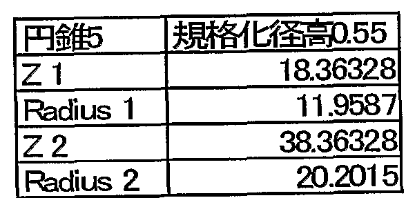
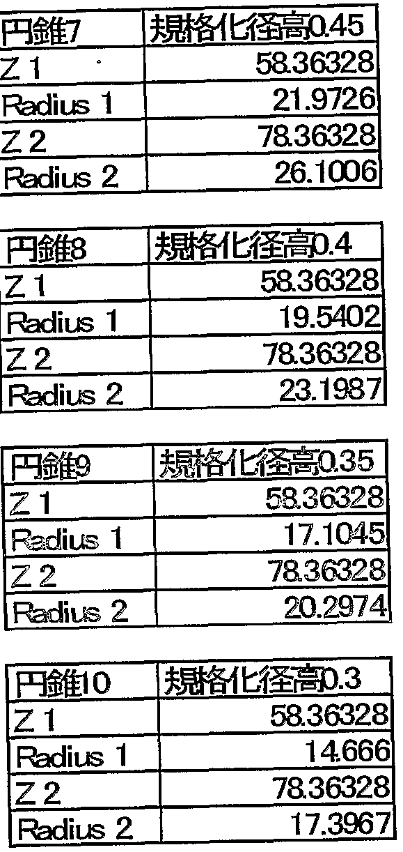
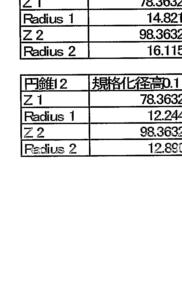
  • Tables 1, 2, 3, and 4 show data of the collimator mirror 12 ′.
  • the unit of the numerical value in the table is [mm] unless otherwise specified (the same applies to other tables).
  • the collimator mirror 1 2 ′ of the present embodiment has unit mirrors 12-1 (cone 1), 12-2 (cone 2), , 1 2-1 7 (cone 17), consisting of a total of 17 unit mirrors.
  • Cone 1, Cone 2, ⁇ , and Cone 17 are each divided into a total of four blocks from the entrance side to the exit side: the first block, the second block, the third block, and the fourth block. .
  • Table 1 shows data for each cone in the first block
  • Table 2 shows data for each cone in the second block
  • Table 3 shows data for each cone in the third block
  • Table 4 shows data for each cone in the fourth block.
  • each cone of each block is represented by the coordinates of two points (Z1, Radius1), (Z 2, Radius 2).
  • the coordinates (Zl, Radius 1) and (Z 2, Radius 2) of the two points are obtained by cutting the cone along the plane (YZ plane) that includes the optical axis Z, as shown in the middle circle in Fig. 18. These are the coordinates of both ends of the resulting cross section.
  • the “normalized diameter height” of each cone refers to the radius of each cone (height in the direction perpendicular to the optical axis Z) and the widest angle in the same block (the angle between the optical axis and the cone). This is the value obtained by dividing the open angle of the cone by the maximum open angle.
  • FIG. 19 is an optical path diagram showing a configuration of the fly-eye mirror 13 of the present embodiment. As shown in Fig. 19, the entrance end 13 in of the fly-eye mirror 13 has 10 unit mirrors 13 in— 1, 13 in-2, ⁇ ⁇ ⁇ , 13 i ⁇ -10 Are shifted by 3 mm in the Y direction.
  • the output end 13 out of the fly-eye mirror 13 is composed of 10 unit mirrors 13 out— 1, 13 out—2,. They are staggered.
  • Table 5 shows fly eye mirror data.
  • the incident end 13 in of the fly-eye mirror 13 of the present embodiment has a Y-direction. A maximum of 43 mirrors and a maximum of 13 mirrors in the X direction can be placed.
  • Table 6 shows the areas (points A, B, C, and D) corresponding to points A, B, C, and D of the capacitor mirror 14 described later. An inclination is provided by the indicated angle.
  • FIG. 20 is an optical path diagram showing the configuration of the condenser mirror 14 of the present embodiment.
  • the condenser mirror 14 has a total of three unit mirrors of unit mirrors 14-1, 14-2, and 14-13 arranged in order from the side of the fly-eye mirror 13.
  • Table 7 shows the data of the condenser mirror 14.
  • the ray tracing direction (surface order) is opposite to the actual light traveling direction (the direction from the reticle surface R to the fly-eye mirror 13; the unit mirror 14—3 1 4—2 14-1 Order).
  • the reflecting surfaces of the unit mirrors 14-1 14-2 and 14-13 are inclined by 15 ° with respect to the optical axis.
  • the reflecting surfaces of the unit mirrors 14-1, 14-2, 14-13 are each formed of a toroidal aspheric surface.
  • Table 8 shows the toroidal aspheric coefficient of each reflecting surface.
  • the definition of a toroidal aspheric surface is expressed by equation (1).
  • ⁇ in Eq. (1) is the Sag amount of the aspheric surface in the optical axis direction.
  • This example is an example corresponding to the second embodiment.
  • FIG. 21 is a diagram showing the positional relationship between the respective reflecting surfaces of the collimator mirror 12 "of the present embodiment, and is shown in Table 9, Table 10, Table 11, Table 12, Table 13, Table 14, and Table 14.
  • Table 15 shows the data of the collimator mirror 12 ".
  • the collimator mirror 12 "of the present embodiment has the unit mirror 12A described in the second embodiment disposed on the outermost periphery.
  • Table 9 shows data for the unit mirror 12 A.
  • the “light-shielding angle” is the maximum value of the angle between the tangent at each position on the reflecting surface and the light beam incident on that position.
  • the “total length” is the length in the direction of the optical axis Z.
  • the collimator mirror 12 "has unit mirrors 12-1 (cone 1), 12-2 (cone 2), ... 1 2-1 2 (cone 1 2) total 1 2 unit mirrors are provided.
  • Cone 1, cone 2, ⁇ , cone 1 2 are the total of the first block, the second block, the third block, the fourth block, the fifth block, and the sixth block from the entrance side to the exit side, respectively. It is pluralized into one block.
  • Table 10 shows data for each cone of the first block
  • Table 11 shows data for each cone of the second block
  • Table 12 shows data for each cone of the third block
  • Table 13 shows data for each cone of the fourth block.
  • Data shows data for each cone in the fifth block
  • Table 15 shows data for each cone in the sixth block.
  • a ray incident in an angle range corresponding to" normalized diameter height "of 1 to 0.75 is reflected by a partial parabolic reflecting surface (unit mirror 1). 2 A), and the light rays incident within an angle range equivalent to the “normalized diameter height” of 0.75 or less are reflected on the reflecting surface (unit mirror 12-1, 12-2). , ⁇ ⁇ ⁇ ).
  • FIG. 1 A third embodiment of the present invention will be described based on FIG.
  • This example is an example corresponding to the third embodiment.
  • FIG. 22 shows the shape of the reflecting surface of the unit mirror 13, i n — l, 13 ′ in—2, 1 ⁇ 2 ⁇ placed at the entrance end 13 in in of the fly-eye mirror 13 'of the present embodiment.
  • the shape of the reflecting surfaces of the unit mirrors 13'in_l, 13 and inn-2, 2 and 3 is an Alternator I type as described in the third embodiment.
  • the dimensions of each part of the alternator I shape are as follows.
  • the shape of the reflecting surface of the unit mirror L3, out—1, 13, 3, out—2, '′ ⁇ placed at the exit end 13 ′ out of the fly-eye mirror shown in the embodiment of FIG.
  • the shape is not limited to this and may be a concave shape or another shape.
  • This example is an example corresponding to the fourth embodiment.
  • FIG. 23 shows the unit mirrors 13 "in-1, 13" in-1, 2, and 3 "arranged at the input end 13" in and the output end 13 "out of the fly-eye mirror 13" of the present embodiment.
  • ⁇ is a diagram illustrating the shape of the reflecting surface.
  • the dimensions of each part of the partial paraboloid are as follows.
  • This example is an example of a fly-eye mirror 33 corresponding to the seventh embodiment and a condenser mirror 14 corresponding to the fly-eye mirror 33.
  • FIG. 24 is an optical path diagram of the fly-eye mirror 33 of the present embodiment.
  • Tables 16 and 17 show fly eye mirror 33 data.
  • Table 17 shows that the upper unit mirror pair (33 in—1, 33 out—1) is based on the central unit mirror pair (33 in—2, 33 out—2).
  • the shift amount (shift amount) of the lower unit mirror pair (33 in-3, 33 out-3) is shown.
  • the Z axis and the Y axis are the traveling direction of the light incident on the fly-eye mirror 33 and the direction perpendicular to the Z axis, respectively.
  • FIG. 25 is an optical path diagram showing the configuration of the condenser mirror 14 of the present embodiment.
  • Table 18 shows the data of the condenser mirror 14.
  • the ray tracing direction (surface order) is opposite to the actual light traveling direction (the direction from the reticle surface R to the fly-eye mirror 33, the unit mirrors 14—3, 14—2, and 14). — 1).
  • the reflecting surfaces of the unit mirrors 14-1, 14-2, 14-13 are inclined by 14 ° with respect to the optical axis.
  • the principal ray at each image height forms an angle of 6 ° with respect to the surface normal.
  • the formation surface of the secondary light source group on the emission end 33 out side of the fly-eye mirror 33 makes an angle of 20 ° with the optical axis.
  • the reflecting surfaces of the unit mirrors 14_1, 14-2, and 14-13 are each formed of a toroidal aspheric surface.
  • Table 19 shows the toroidal aspheric coefficient of each reflecting surface. Note that the definition of the toroidal aspheric surface is given by equation (1). [Table 19]
  • the illumination efficiency of the illumination optical system is considered.
  • the fly-eye mirror 13, 13 ', 13 " as a reflective optical integrator that can achieve both high illumination efficiency and uniform illumination is described below. , 3 3) will be briefly described.
  • the fly-eye mirrors (13, 13 ', 13 ", 33) as reflection optical integrators in each of the above embodiments and examples are arranged on the incident side and have a large number of unit mirrors (first to third mirrors). 1st mirror (1 3 i) n, 13 'in, 13 "in, 33 in) and a second array of mirrors (1 3 out, 13 3) arranged on the emission side and having a number of unit mirrors (second reflecting elements). 'out, 13 "out, 33 out).
  • the light incident on the fly-eye mirror is divided into a large number of lights by a large number of unit mirrors of each array mirror, and the divided light is divided by a reticle (mask) and a wafer (photosensitive substrate).
  • the reticle (mask) and wafer (photosensitive substrate) are uniformly illuminated by the fly-eye mirror (13, 13, 13, 13 ", 33) to illuminate the formed illumination area in a superimposed manner. You.
  • 1 3 in, 1 3 'in, 1 3 "in, 3 3 in) and the second array mirror (1 3 out, 1 3' out, 1 3" out, 33 out) are in meridional direction and sagittal. It has a large number of unit mirrors (first and second reflecting elements) having a predetermined optical power in the direction, and therefore, has a fly-eye mirror (13, 13 ', 13 ", 3").
  • the light incident on (3) is split into wavefronts.
  • this fly-eye mirror (13, 13 ', 13 ", 33) At the exit side or near the exit side of this fly-eye mirror (13, 13 ', 13 ", 33), a number of focal points as secondary light sources are formed.
  • the fly-eye mirror (13, 13) is located at the position of the pupil (entrance pupil) of the reflective projection optical system shown in FIG. , 1 3 ", since the image of the secondary light source by the 3 3) are formed, the reticle (mask) and a wafer (photosensitive substrate) is Koehler illumination as uniform illumination is achieved.
  • the reticle (mask) and wafer (photosensitive substrate) can be made more uniform while suppressing the light amount loss in the fly-eye mirror by the involvement of the total reflection fly-eye mirror in each embodiment and each example. Be illuminated.
  • the entrance side of the fly-eye mirror (1 3, 13 ', 13 ", 33), that is, the first array mirror (1 3 in, 1 3' in, 13" in, 33 in) The entrance side is located at a position that is substantially optically conjugate with the reticle (mask) and wafer (photosensitive substrate).
  • the first arrayed mirror 13 in, 1
  • the shape of the many unit mirrors (first reflective elements) that make up 3 'in, 13 "in, 33 in) is formed on a reticle (mask) or wafer (photosensitive substrate). It is similar to the shape of the illumination area.
  • the exit side of the fly-eye mirror (1 3, 13, 3, 13 ", 33), that is, the second array mirror (1 3 out, 1 3 'out, 1 3" out, 3 3 out) is For example, it is located substantially optically conjugate with the pupil (entrance pupil) of the projection optical system shown in FIG.
  • a large number of first reflecting elements (33 in-1, 33) in the first array mirror 33 in are provided.
  • the incident light the light at the center of the incident light or the reticle
  • the first reflection elements 33 in-1, 1, 33 in-2,.
  • a light passing through the center of the illumination field of view at a first reference plane P1 inclined at a predetermined angle ⁇ 1.
  • a number of the second reflecting elements (33 out-1, 33 out -2,...) In the second array mirror 33 3 out are connected to the second reflecting element (33 out-1).
  • the fly-eye mirror (13, 13, 13, 13 ", 33) as a reflective optical integrator is composed of two array-like mirrors (raster).
  • the fly-eye mirror (13, 13, 13, 13 ", 33) can be composed of a single array mirror (raster mirror). is there.
  • An example was shown in which a reflection member that totally reflected all light was used. It is possible to use a member that has a small contribution to the condition as needed.
  • the member having a small contribution to the image formation of the illumination optical system may be a transmissive member or a reflecting member appropriately deviating from the condition of total reflection, and these members can be applied in the present invention. Needless to say.
  • a mask (reticle) is illuminated by an illumination optical system or an illumination optical device (illumination step), and a transfer pattern formed on the mask using the projection optical system.
  • a micro device semiconductor element, imaging element, liquid crystal display element, thin film magnetic head, etc.
  • FIG. 1 An example of a method for obtaining a semiconductor device as a microphone device by forming a predetermined circuit pattern on a wafer or the like as a photosensitive substrate using the exposure apparatus of the above-described embodiment is shown in FIG. This will be described with reference to a flow chart.
  • a metal film is deposited on one lot of wafers.
  • a photoresist is applied on the metal film on the wafer of the lot.
  • the image of the pattern on the mask is sequentially exposed to each shot area on that one lot of wafers via the projection optical system. Transcribed.
  • the photoresist on the one lot of wafers is developed, and in step 300, the resist pattern is masked on the one lot of wafers to perform etching.
  • a circuit pattern corresponding to the pattern on the mask is formed in each shot area on each wafer.
  • devices such as semiconductor elements are manufactured by forming a circuit pattern of the upper layer. According to the above-described semiconductor device manufacturing method, a semiconductor device having an extremely fine circuit pattern can be obtained with good throughput.
  • a liquid crystal display element as a micro device can be obtained by forming a predetermined pattern (circuit pattern, electrode pattern, etc.) on a plate (glass substrate).
  • a so-called photolithography step in which a mask pattern is transferred and exposed to a photosensitive substrate (a glass substrate coated with a resist or the like) using the exposure apparatus of the above-described embodiment. Is executed.
  • a photolithography process a predetermined pattern including a large number of electrodes and the like is formed on the photosensitive substrate.
  • the exposed substrate is subjected to a developing process, an etching process, a resist peeling process, and the like, whereby a predetermined pattern is formed on the substrate, and the process proceeds to the next color filter forming process 402. .
  • a large number of sets of three dots corresponding to R (Red), G (Green), and B (Blue) are arranged in a matrix, or R, G,
  • a color filter is formed by arranging a set of three stripe filters B in the horizontal scanning line direction.
  • a cell assembling step 403 is performed.
  • a liquid crystal panel liquid crystal cell
  • liquid crystal is injected between the substrate having the predetermined pattern obtained in the pattern forming step 401 and the color filter obtained in the color filter forming step 402.
  • liquid crystal panels liquid crystal cells
  • each component such as an electric circuit and a backlight for performing a display operation of the assembled liquid crystal panel (liquid crystal cell) is attached to complete a liquid crystal display element.
  • an illumination optical system and an illumination device with small loss of light amount can be realized.
  • a high-performance projection exposure apparatus capable of achieving a high throughput by remarkably improving the illumination efficiency, and a good microdepth (semiconductor device, image sensor, liquid crystal display device, thin-film magnetic head, etc.) To realize an exposure method that can manufacture be able to.
  • the fly-eye mirror of the present invention which satisfies the condition of total reflection, can improve the illumination efficiency and achieve uniform illumination at the same time, and can significantly improve the performance of the illumination optical system, the illumination device, and the projection exposure device. It is possible to do. This makes it possible to achieve an exposure method capable of producing a finer microphone opening depice under a high throughput.

Landscapes

  • Physics & Mathematics (AREA)
  • General Physics & Mathematics (AREA)
  • Spectroscopy & Molecular Physics (AREA)
  • Engineering & Computer Science (AREA)
  • General Engineering & Computer Science (AREA)
  • High Energy & Nuclear Physics (AREA)
  • Exposure And Positioning Against Photoresist Photosensitive Materials (AREA)
  • Exposure Of Semiconductors, Excluding Electron Or Ion Beam Exposure (AREA)

Abstract

本発明は、光源にEUV光を用いた場合においても光量ロスの少ない照明光学系等を提供することを目的とする。本発明の照明光学系は、極端紫外光を射出する光源部、コリメータミラー、フライアイミラー、及びコンデンサミラーを順に配置し、前記コリメータミラー、フライアイミラー、コンデンサミラーの各々は、入射光の斜入射角度が全反射角度となる姿勢で配置された複数の単位ミラーからなることを特徴とする。

Description

明細書
照明光学系、 照明装置、 投影露光装置、 及び露光方法 技術分野
本発明は、 投影露光装置に搭載される照明光学系や照明装置に関し、 特に、 極 端紫外光 (Extreme Ultra Violet光:以下、 EUV光という。 ) に適した照明光 学系や照明装置に関する。 また、 本発明は、 上記照明光学系及び照明装置を用い た投影露光装置に関する。 また、 本発明は、 これらの照明光学系や照明装置を用 いて良好なるマイクロデバイス (半導体装置、 撮像素子、 液晶表示装置、 薄膜磁 気ヘッド等) を製造するための露光方法に関する。 背景技術
投影露光装置は、 半導体の集積密度を向上させるため、 露光波長が短波長化さ れる傾向にある。
それに適用される光源としては、 水銀の i線 (波長 365. 0 1 5 nm) 、 r Fエキシマレーザ (波長 248 nm) 、 A r Fエキシマレーザ (波長 1 93 n m) 、 F2エキシマレーザ (波長 1 5 7 nm) などが挙げられる。 さらには、 E UV光、 特に波長 50 nm以下の EUV光を光源として用いることも検討されて いる。
仮に、 波長 50 nm以下の EUV光を用いる場合、 光学系を反射型に構成する 必要が生じる (たとえば、 特開 2000— 349009号公報に記載された照明 光学系など。 ) 。
しかしながら、 特開 2000— 349009号公報に記載された照明光学系で あっても、 EUV光、 特に波長 50 nm以下の EUV光を十分な反射率で反射さ せることはできないので、 光量ロスが大きい。
なお、 各反射面に多層膜を用いることで或る程度の改善が図られるが、 それで もこの照明光学系では各反射面につき 70%程度しか反射率が得られないので、 不十分である。
また、 照明光学系中に配置されたフライアイミラーにおける光量ロスも多くフ ライアイミラーそのものにて大幅な改善が求められている。 発明の開示
そこで本発明は、 光源に E U V光を用いた場合においても光量ロスの少ない照 明光学系及び照明装置を提供することを提供することを目的とする。
また、 本発明は、 上記照明光学系及び照明装置を用いることによって高性能な 投影露光装置を提供することを目的とする。
さらに、 本発明は、 上記照明光学系及び照明装置を用いることによって良好な るマイクロデバイス (半導体装置、撮像素子、 液晶表示装置、 薄膜磁気へッド等) を製造し得る露光方法を提供することを目的とする。
本発明の照明光学系は、 極端紫外光を射出する光源部、 コリメータミラー、 フ ライアイミラー、 及びコンデンサミラーを順に配置し、 前記コリメータミラー、 フライアイミラー、 コンデンサミラーの各々は、 入射光の斜入射角度が全反射角 度となる姿勢で配置された複数の単位ミラーからなることを特徴とする。
好ましくは、 前記光源部は、 レーザプラズマ光源と、 前記レーザプラズマ光源 から出射された極端紫外光を集光するコレクタミラーと、 前記コレクタミラーに よる前記極端紫外光の集光点近傍に配置された飛散物遮断用の隔壁とを備える。 また、 好ましくは、 前記光源部は、 放電プラズマ光源を備えている。
さらに、 好ましくは、 前記光源部は、 前記放電プラズマ光源から出射された極 端紫外光を集光するコレクタミラーと、 前記コレクタミラーによる前記極端紫外 光の集光点近傍に配置された飛散物遮断用の隔壁とを備える。
さらに、 好ましくは、 前記コレクタミラーは、 入射光の斜入射角度が全反射角 度となる姿勢で配置された複数の単位ミラーからなる。
さらに、 好ましくは、 前記コリメータミラーは、 互いに径及び広がり角度の異 なる複数のスカート状の単位ミラーを、 その広がり部を射出側に向けた状態で光 軸の周りに配置してなる。
さらに、 好ましくは、 前記複数のスカート状の単位ミラーの反射面は、 円錐の 部分側面の形状をしている。
また、 好ましくは、 前記単位ミラーのうち最外周側に配置される前記単位ミラ 一の反射面は、放物面の形状をしており、それ以外の前記単位ミラーの反射面は、 円錐の部分側面の形状をしている。
さらに、好ましくは、前記コリメ一タミラーと前記フライアイミラーとの間に、 複数の中空管を並列配置してなるキヤビラリーアレイが配置される。
さらに、 好ましくは、 前記キヤビラリーアレイを冷却する冷却機構が備えられ る。
さらに、 好ましくは、 前記フライアイミラーは、 互いに同姿勢の複数の単位ミ ラーを並列配置した入射端と、 互いに同姿勢の複数の単位ミラーを並列配置した 出射端とを、 それら各単位ミラーに対する入射光の斜入射角度が全反射角度とな るよう、 それら単位ミラーによる反射光の進行方向に十分な間隔をおいて配置し てなる。
さらに、 好ましくは、 前記入射端に配置される前記複数の単位ミラーの反射面 は、 それぞれゥオルター I型の形状をしている。
さらに、 好ましくは、 前記入射端及び前記出射端に配置される前記複数の単位 ミラーの反射面は、 それぞれ放物面の形状をしている。
さらに、 好ましくは、 前記入射端を構成する前記複数の単位ミラーは、 各単位 ミラー間の反射光のケラレが低減されるよう、 それら単位ミラーによる反射光の 進行方向に十分な距離ずつずらして配置され、 前記出射端を構成する前記複数の 単位ミラーは、 各単位ミラー間の反射光のケラレが低減されるよう、 それら単位 ミラーによる反射光の進行方向に十分な距離ずつずらして配置される。
さらに、 好ましくは、 前記コンデンサミラーは、 複数の単位ミラーを直列配置 してなり、 かつそのうち少なくとも 1つの反射面がトロイダル非球面である。 さらに、 好ましくは、 前記光源部が射出する前記極端紫外光は、 波長 5 0 n m 以下の極端紫外光であり、 前記コリメータミラー、 フライアイミラー、 コンデン サミラーの各単位ミラーの反射面は、 R u又は M oの材料からなり、 かつ前記斜 入射角度が 1 5 ° 以下となる姿勢で配置される。
本発明の投影露光装置は、 反射型の投影光学系と、 本発明の何れかの照明光学 系とを備えたことを特徴とする。
本発明の露光方法は、 本発明の何れかの照明光学系を用いてレチクルを照明す る照明工程と、 前記レチクルのパターンを感光性基板に露光する露光工程とを含 むことを特徴とする。
本発明の照明装置は、 極端紫外光を供給する光源部、 及び該光源部からの光を 被照明物体に導く照明光学系を有し、 前記照明光学系は、 前記極端紫外光を反射 させる複数の反射部材を含み、前記照明光学系を構成する全ての前記反射部材は、 入射光の入射角度が全反射角度となる姿勢で配置されることを特徴とする。
好ましくは、 前記複数の反射部材は、 多数の反射素子を有するアレイ状ミラー を少なくとも含み、 前記アレイ状ミラーにおける多数の反射素子は、 入射光の入 射角度が全反射角度となる姿勢で配置される。
さらに好ましくは、 前記アレイ状ミラーにおける多数の反射素子は、 メリジォ ナル方向及びサジタル方向において所定の光学パワーをそれぞれ有する。
さらに好ましくは、 前記複数の反射部材は、 多数の第 1の反射素子を有する第 1のアレイ状ミラーと、 多数の第 2の反射素子を有する第 2のアレイ状ミラーと を少なくとも含み、 前記第 1のアレイ状ミラーにおける多数の第 1の反射素子及 び前記第 2のアレイ状ミラーにおける多数の第 2の反射素子は、 入射光の入射角 度が全反射角度となる姿勢でそれぞれ配置される。
また、 本発明の照明装置は、 極端紫外光を供給する光源部、 及び該光源部から の光を被照明物体に導く照明光学系を有し、 前記照明光学系は、 前記極端紫外光 を反射させる複数の反射部材を含み、 前記複数の反射部材は、 多数の第 1の反射 素子を有する第 1のアレイ状ミラーと、 多数の第 2の反射素子を有する第 2のァ レイ状ミラーとを少なくとも含み、 前記第 1のアレイ状ミラ一における多数の第 1の反射素子及び前記第 2のアレイ状ミラーにおける多数の第 2の反射素子は、 入射光の入射角度が全反射角度となる姿勢でそれぞれ配置されることを特徴とす る。
好ましくは、 前記第 1のアレイ状ミラーにおける多数の第 1の反射素子及び前 記第 2のアレイ状ミラーにおける多数の第 2の反射素子は、 メリジォナル方向及 びサジタル方向において所定の光学パワーを有する。
さらに好ましくは、 前記第 1のアレイ状ミラ一及び前記第 2のアレイ状ミラー を経由した光は、前記第 2のアレイ状ミラー、前記第 2のアレイ状ミラーの近傍、 または前記第 2のァレイ状ミラーの射出側に 2次光源としての多数の集光点を形 成する。
さらに好ましくは、 前記第 1の反射素子と第 2の反射素子とのうちの少なくと も一方は方物面状の反射面を含む。
さらに好ましくは、 前記第 1のアレイ状ミラーにおける多数の第 1の反射素子 は、 前記第 1のアレイ状ミラーに入射する入射光路に対して所定の角度で傾斜す る第 1の基準面にて稠密に配置され、 前記第 2のアレイ状ミラーにおける多数の 第 2の反射素子は、 前記第 2のアレイ状ミラーに入射する入射光路を所定の角度 で傾斜する第 2の基準面にて稠密に配置されることを特徴とする。
さらに好ましくは、 前記第 1のアレイ状ミラーにおける多数の第 1の反射素子 は、 前記多数の第 1の反射素子の各々に入射する光の中心光に対して所定の角度 ^ 1 で傾斜する第 1の基準面にて稠密に配置され、 前記第 2のアレイ状ミラーに おける多数の第 2の反射素子は、 前記多数の第 1の反射素子の各々に入射する光 の中心光に対して所定の角度 ]3 2 で傾斜する第 2の基準面にて稠密に配置され、 前記所定の角度 1 及び前記所定の角度 2 は、 0 ° く ]3 1≤ 2 0 ° 、 0 ° く β 2
2 0 ° を満たす。
本発明の投影露光装置は、 本発明の何れか 照明装置と、 前記照明装置により 照明された前記被照明物体としてのレチクルのパターンを感光性基板に投影する 投影光学系とを有することを特徴とする。
本発明の露光方法は、 本発明の何れかの照明装置を用いて前記被照明物体とし てのレチクルを照明する照明工程と、 前記レチクルのパターンを感光性基板に露 光する露光工程とを含むことを特徴とする。
本発明の露光方法は、 極端紫外光を供給する工程と、 該極端紫外光でレチクル を照明する工程と、 前記レチクルのパターンを感光性基板に露光する工程とを含 み、 前記照明工程は、 入射光の入射角度が全反射角度となる姿勢で配置された複 数の反射部材のみを用いて前記極端紫外光を被照明物体へ導く工程を含むことを 特徴とする。
本発明の露光方法は、 極端紫外光を供給する工程と、 該極端紫外光でレチクル を照明する工程と、 前記レチクルのパターンを感光性基板に露光する工程とを含 み、 前記照明工程は、 入射光の入射角度が全反射角度となる姿勢で配置された多 数の第 1の反射素子を有する第 1のアレイ状ミラーと、 入射光の入射角度が全反 射角度となる姿勢で配置された多数の第 2の反射素子を有する第 2のアレイ状ミ ラーとを用いて前記極端紫外光を被照明物体へ導く工程を含むことを特徴とする。 図面の簡単な説明
図 1は、 第 1実施の形態の照明光学系の概略構成図である。
図 2は、 波長 1 3. 5 nmの EUV光の斜入射角度と反射率との関係 (M oに ついて) を示す図である。
図 3は、 波長 1 3. 5 nmの EUV光の斜入射角度と反射率との関係 (R uに ついて) を示す図である。
図 4は、 波長 1 3. 5 nmの EUV光の斜入射角度と反射率との関係 (M o S i 2について) を示す図である。
図 5は、 第 1実施の形態のコリメータミラー 1 2を説明する図である。
図 6は、 第 1実施の形態のコリメータミラー 1 2' を説明する図である。
図 7は、 (a) は第 1実施の形態のフライアイミラー 1 3の入射端 1 3 i nを 示す図であり、 (b) は第 1実施の形態のフライアイミラー 1 3の出射端 1 3 o u tを示す図である。
図 8は、 第 1実施の形態のフライアイミラー 1 3の入射端 1 3 i nに配置され た単位ミラー 1 3 i n— 1 , 1 3 i n— 2, · · ·の反射面の形状を説明する図 である。
図 9は、 第 2実施の形態のコリメータミラー 1 2" を説明する図である。
図 1 0は、 キヤビラリ一アレイ 1 2 Bを説明する図である。
図 1 1は、 第 3実施の形態のフライアイミラー 1 3, の入射端 1 3 ' i nに配 置された単位ミラー 1 3 ' i n- 1 , 1 3 ' i n— 2, · ■ ■の反射面の形状を 説明する図である。
図 1 2は、 第 4実施の形態のフライアイミラー 1 3" の入射端 1 3" i nに配 置された単位ミラー 1 3" i n— 1, 1 3" i n— 2, · · ·、 及ぴ出射端 1 3 " o u tに配置された単位ミラー 1 3" o u t _ l, 1 3" o u t— 2, · ■ ' の 反射面の形状を説明する図である。
図 1 3は、 第 5実施の形態の光源部 2 1、 及びその周辺の概略構成を示す図で める。
図 14は、 第 6実施の形態の光源部 3 1、 及びその周辺の概略構成を示す図で ■ める。
図 1 5は、 第 6実施の形態のコレクタミラー 3 1 cを説明する図 (透視図) で める。
図 1 6は、 第 7実施の形態のフライアイミラー 3 3の各単位ミラーの配置関係 を説明する図である。
図 1 7は、 第 8実施の形態の投影露光装置の構成図である。
図 1 8は、 第 1実施例のコリメータミラー 1 2, の構成を示す断面図である。 図 1 9は、 第 1実施例のフライアイミラー 1 3の構成を示す光路図である。 図 20は、 第 1実施例のコンデンサミラー 14の構成を示す光路図である。 図 2 1は、 第 2実施例のコリメータミラー 1 2" の各反射面の位置関係を示す 図である。
図 22は、 第 3実施例のフライアイミラー 1 3' の入射端 1 3 ' i nに配置さ れた単位ミラー 1 3, i n— 1, 1 3, 一 2, ■ ■ ■の反射面の形状を説明する 図である。
図 2 3は、 第 4実施例のフライアイミラー 1 3" の入射端 1 3" i n及び出射 端 1 3,, o u tに配置された単位ミラー 1 3" i n - 1 , 1 3" i n— 2, ■ · ■, 1 3" o u t— 1, 1 3" o u t— 2, ■ · 'の反射面の形状を説明する図であ 。
図 24は、 第 5実施例のフライアイミラー 3 3の光路図である。
図 2 5は、 第 5実施例のコンデンサミラー 14の構成を示す光路図である。 図 26は、 マイクロデバイスとしての半導体デバイスを得る際の手法のフロー チヤ一トである。
図 27は、 マイクロデバイスとしての液晶表示素子を得る際の手法のフローチ ヤートである。 発明を実施するための最良の形態
以下、 図面に基づいて本発明の実施の形態について説明する。
[第 1実施の形態]
図 1、 図 2、 図 3、 図 4、 図 5、 図 6、 図 7、 図 8に基づいて本発明の第 1実 施の形態について説明する。 本実施の形態は照明光学系の実施の形態である。 図 1は、 本実施の形態の照明光学系の概略構成図である。 なお、 図 1において 符号 1 2 A, 1 2 B, 1 2 C, 1 3 ' , 1 3" が付与されたのは、 後述する実施 の形態の構成要素なのでここでは説明しない。
この照明光学系は、主に反射型の投影光学系を備えた投影露光装置に適用され、 その投影露光装置のレチクル面 Rをケーラー照明するものである。
この照明光学系の光源部 1 1は、 EUV光 (以下、 波長 50 nm以下の EUV 光とする。 ) を射出する光源部である。
この光源部 1 1には、 効率のよい X eをターゲットとして用いたレーザプラズ マ光源、 又は、 放電プラズマ光源などが適用可能である。
特に、 放電プラズマ光源は、 エネルギー効率が比較的高いので、 高いスループ ットを実現する上で有利である。
照明光学系には、 この光源部 1 1の射出側に、 コリメータミラー 1 2、 フライ アイミラー 1 3、 及びコンデンサミラー 14が順に配置される。
コリメータミラー 1 2は、 複数の単位ミラー 1 2— 1, 1 2- 2, · · ·を入 射光束に対し並列配置している。
フライアイミラー 1 3は、複数の単位ミラー 1 3 ΐ η- 1 , 1 3 ί η- 2, · · · を並列配置した入射端 1 3 i η、 複数の単位ミラー 1 3 o u t— 1, 1 3 o u t 一 2, ■ ■ 'を並列配置した出射端 1 3 o u tを有する。
コンデンサミラー 14は、 複数の単位ミラー 14一 1, 14- 2, ■ · ·を入 射光束に対し直列配置している。
ここで、 並列配置とは、 入射光束のうち互いに異なる部分光束に対し個別に作 用する配置であり、 また、 直列配置とは、 入射光束の全体に対し順に作用する配 置である。
そして、 これらの単位ミラー 1 2— 1, 1 2- 2, · · ■, 1 3 i n - 1 , 1 3 i n - 2 , ■ ■ ·, 1 3 o t - 1 , 1 3 o u t - 2 , · · ·, 14— 1, 1 4- 2, ■ · ·の姿勢は、 それらの反射面に対する入射光 (ここでは、 波長 50 nm以下の EUV光) の斜入射角度 (反射面とのなす角度) がそれぞれ全反射角 度となるよう設定される。
なお、 理想的な全反射は反射率 100%の反射であるが、 実際には若干の光量 ロスは許容せざるを得ないので、 本明細書では、 文言 「全反射」 を、 「反射率 8 0%以上の反射」 とし、 入射光が全反射する斜入射角度を特に、 「全反射角度」 という。
また、 これらの単位ミラー 1 2- 1 , 1 2- 2, ■ ■ ■, 1 3 i n - 1 , 1 3 i n— 2, ■ ■ ■, 1 3 o u t— 1 , 1 3 o u t— 2 , · ■ ■, 14— 1 , 14 一 2, · · ' の反射面には、 それぞれ Mo又は Ruの材料が使用される。
図 2、 図 3、 図 4は、 波長 1 3. 5 nmの EUV光の斜入射角度と反射率との 関係を示す図である。
図 2に示すのは Moの反射率、 図 3に示すのは R uの反射率、 図 4に示すのは Mo S i 2の反射率である。
これらは何れも反射面に使用される代表的な材料であるが、 何れも、 入射光の 斜入射角度が小さいほど反射率が高くなる。
図 2、 図 3、 図 4によると、 Moの全反射角度は約 1 5° 以下、 Ruの全反射 角度は約 1 5° 以下、 Mo S i 2の全反射角度は約 10° 以下である。
特に、 反射率が 90%以上得られる全反射角度は、 Moについては約 10° 以 下、 R uについては約 8° 以下、 Mo S i 2については約 5° 以下である。
つまり、 M o又は R uの材料を使用した場合の全反射角度は、 Mo S i 2の材 料を使用した場合の全反射角度と比較すると大きい。
本実施の形態では、 単位ミラー 1 2— 1, 1 2 - 2, · · · , 1 3 i n - 1 , 13— i n— 2, · · ·, 1 3 o u t— 1 , 1 3 o u t— 2 , ■ · ■, 14- 1, 14- 2, · ■ 'の反射面にそれぞれ Mo又は R uの材料が使用されるので、 全 反射角度は比較的大きい 1 5° 以下となる。
したがって、 各反射面の配置設計の自由度は、 他の材料を使用した場合よりも 高くなる。 但し、 s; p偏光間の反射率の違いによる強度差が問題となるような場合には、 各反射面の一部又は全部に Mo S i 2の材料を用いればよい。
図 5は、 本実施の形態のコリメータミラー 1 2を説明する図である。
図 5 (a) は光軸 Zを含む平面でコリメータミラー 1 2を切断した断面図、 図 5 (b) はコリメータミラー 1 2の斜視図である。
図 5 (a) に示すように、 コリメータミラー 1 2は、 互いに径及ぴ広がり角度 の異なる複数のスカート状の単位ミラー 1 2— 1, 1 2— 2, · · ·を、 その裾 部 (広がり部) を射出側に向けた状態で光軸 Zの周りに配置している (図では、 単位ミラーの数を 3とした。 ) 。
単位ミラー 1 2— 1 , 1 2 - 2, · ■ ·は、 それぞれ内側に反射面を有してい る。
入射光束を平行光束に変換するに当たり、 周辺光線を偏向する単位ミラー (つ まり径が大きく外側に配置された単位ミラー) ほど、 その広がり角度が大きく採 られる。
また、 単位ミラー 1 2— 1 , 1 2 - 2 , · · ■の反射面は、 図 5 (a) (b) にも示すように、 それぞれ円錐の部分側面の形状とされる。
このような単位ミラー 1 2— 1 , 1 2 - 2, · ■ ·からなるコリメータミラー 1 2は、 光源部 1 1から互いに異なる射出角度で射出した光線を個別に平行光束 に変換する。
ここで、 このコリメータミラー 1 2においては、 上述したように単位ミラー 1 2— 1, 1 2— 2, · · 'の反射面に対する入射光の斜入射角度 0 (図 5 (a) 参照) が、 それぞれ全反射角度 (ここでは 1 5° 以下) に抑えられなければなら ない。
しかし、 この構成では、 コリメータミラー 1 2における全ての入射光の斜入射 角度を全反射角度 (ここでは 1 5° 以下) にすることはできない可能性がある。 特に、 径の大きい単位ミラー (外側に配置された単位ミラー) に対する入射光の 斜入射角度が全反射角度(ここでは 1 5° 以下)よりも大きくなる可能性がある。 その場合、 コリメータミラー 1 2を図 6に示すコリメータミラー 1 2, のよう に変形するとよい。 図 6は、 コリメータミラー 1 2' を説明する図である。
図 6 (a) は光軸 Zを含む平面でコリメータミラー 1 2' を切断した断面図、 図 6 (b) はコリメータミラー 1 2' の斜視図である。
コリメータミラー 1 2' の最外周に配置された単位ミラー 1 2— 1は、 複数の 単位ミラー 1 2— 1— 1, 1 2— 1— 2, · · 'を直列配置している (図 6では、 直列配置される単位ミラーの数を 3とした。 ) 。
単位ミラー 1 2— 1— 1, 1 2— 1— 2, · · ·のそれぞれは、 図 5に示した コリメータミラー 1 2の単位ミラー 1 2— 1と同様、 ス力 ト状をしており、 そ の反射面が円錐の部分側面の形状をしている。
単位ミラー 1 2— 1— 1, 1 2— 1— 2, 1 2— 1— 3, · · 'は、 光源部 1
1側からの入射光を順に反射することにより、 その入射光を光軸 zに平行な光線 に変換して射出する。
なお、 最外周以外の単位ミラー 1 2— 2, 1 2- 3, · · ■のそれぞれについ ても同様に、 複数の単位ミラーを直列配置させてもよい (1 2— 2— 1, 12- 2— 2, 1 2— 2— 3, 1 2— 3— 1, 1 2— 3— 2, 1 2— 3— 3) 。
次に、 フライアイミラー 1 3 (図 1参照) について説明する。
上述したようにこのフライアイミラー 1 3の単位ミラー 1 3 i n_ 1 , 1 3 i n - 2 , · ■ · , 1 3 o u t - 1 , 1 3 o u t - 2 , · · ·の姿勢は、 それぞれ 入射光の斜入射角度が全反射角度(ここでは 1 5° 以下)となるよう設定される。 このため、 フライアイミラー 1 3の入射端 1 3 i nと出射端 1 3 o u tとは、 それら各単位ミラーによる反射光の進行方向に十分な間隔をおいて配置される。 図 7は、 フライアイミラー 1 3を説明する図である。
図 7 (a) にはフライアイミラー 1 3の入射端 1 3 i n、 図 7 (b) にはフラ ィアイミラー 1 3の出射端 1 3 o u tを示した。 なお、 図 7 (a) はコリメータ ミラー 1 2の側から見た様子であり、 図 7 (b) はコンデンサミラー 14の側か ら見た様子である。
図 8は、 フライアイミラー 1 3の入射端 1 3 i nに配置される単位ミラー 1 3 i n— 1, 1 3 i n- 2, ■ ■ ·の反射面の形状を説明する図である。
単位ミラー 1 3 i n— 1, 1 3 i n- 2, · · ·の反射面は、 出射端 1 3 o u tに配置される単位ミラー 1 3 o u t— 1, 1 3 o u t - 2, · ■ ■上にそれぞ れ二次光源を収差無く形成するため、 それぞれ部分放物面の形状をしている。 また、 単位ミラー 1 3 i n— 1, 1 3 i n- 2, · · ■の反射面の外形は、 投 影露光装置の露光領域と相似形をしている。 ここでは、 露光領域が円弧フィール ドであるとする。
次に、 コンデンサミラー 14 (図 1参照) について説明する。
コンデンサミラー 14は、 出射端 1 3 o u tから射出する光束を、 単位ミラー 14- 1, 14-2, · · 'にて順に反射し、 出射端 1 3 o u Uこ形成された二 次光源群をレチクル面 R上の円弧フィールドに重畳して投影する。
これら単位ミラー 14一 1 , 14- 2, · · ' の少なくとも 1つの反射面の形 状は、 後述する式 (1) により定義される 「トロイダル非球面」 である。
以上説明した光源部 1 1、 コリメータミラー 1 2 (又は 1 2 ' ) 、 フライアイ ミラー 1 3、 コンデンサミラー 14からなる本実施の形態の照明光学系は、 各ミ ラーを複数の単位ミラーにより構成すると共に、 全ての反射面の全反射作用を利 用しているので、 EUV光の光量ロスは少なく抑えられる。
このような照明光学系によれば、 レチクル面 Rは十分な光量の EUV光により 照明される。
また、 本実施の形態の照明光学系では、 各反.射面に対する斜入射角度を積極的 に全反射角度 (ここでは 1 5° ) としているので、 それら各反射面に多層膜を形 成する必要は無い。
また、 本実施の形態の照明光学系では、 コリメータミラー 1 2の単位ミラー 1 2— 1 , 1 2- 2, · · ·の反射面を比較的単純な円錐の部分側面の形状として いるが、 円錐の部分側面は、 発散する光束を平行光束に変換するための理想的形 状である部分放物面 (放物面の一部の面) に似ているだけでなく、 その部分放物 面よりも単純な曲面である。
よって、 単位ミラー 1 2— 1, 1 2- 2, · · ■は、 所望の機能を果たしなが ら薄化可能である。
単位ミラー 1 2— 1, 1 2- 2, · · 'が薄化されれば、 コリメータミラー 1 2の入射端における光線のケラレが低減されるので、 光量ロスは、 さらに低減さ れる。
また、 図 6に示したコリメータミラー 1 2' が適用されれば、 そのコリメータ ミラー 1 2, において互いに直列に配置された単位ミラー 1 2— 1— 1, 1 2— 1 - 2, · · ·のそれぞれに割り当てられる光線の偏向角度が、 直列に配置され る単位ミラーが単一であるとき (図 5参照) よりも小さいので、 入射光の斜入射 角度をそれぞれ全反射角度 (ここでは 1 5° 以下) とし、 光量ロスを確実に抑え ることができる。
このコリメータミラー 1 2 ' においては、 直列に配置される単位ミラーの数を 多くした分だけ、 各反射の斜入射角度を小さくする (例えば 6° 程度。 その場合 の反射率は 90%以上) ことができる。 このようにすれば、 より高い反射率で全 反射することが可能である。
また、 フライアイミラー 1 3においては、 単位ミラー 1 3 i n_ l, 1 3 i n 一 2, · · ·, 1 3 o u t - 1 , 1 3 o u t - 2 , · ■ 'の姿勢をそれぞれそれ らの反射面に対する入射光の斜入射角度がさらに小さくなるよう (例えば 6° 程 度。 その場合の反射率は 90%以上) 設定すれば、 光量ロスをさらに抑えること ができる。
また、 コンデンサミラー 14の単位ミラー 14_ 1, 14- 2, · · 'の反射 面には、 「トロイダル非球面 J (式 (1) 参照) が用いられるので、 このコンデ ンサミラー 14にて不可避的に発生する非点収差は、 効率的に除去される。
また、コンデンサミラー 14においては、単位ミラー 14— 1, 14- 2, · · · の姿勢をそれぞれそれらの反射面に対する入射光の斜入射角度がさらに小さくな るよう (例えば 6° 程度。 その場合の反射率は 90%以上) 設定すれば、 光量口 スをさらに抑えることができる。
なお、 以上の説明では、 反射面に対する入射光の斜入射角度をなるベく小さく することが望ましいとしたが、 互いに直列配置される単位ミラーの数をそのため に増加する場合、 反射回数の増加による光量ロスの増加を考慮し、 複数の単位ミ ラーの全体における光量ロスが低減されるように設計がなされる必要がある。 〔第 2実施の形態]
図 1、 図 9、 図 10に基づいて本発明の第 2実施の形態について説明する。 本 実施の形態は照明光学系の実施の形態である。
ここでは、 第 1実施の形態の照明光学系との相違点についてのみ説明する。 相 違点は、 図 1に示すコリメータミラー 1 2 (又は 1 2, ) に代えてコリメータミ ラー 1 2" が適用され、 また、 キヤビラリーアレイ 1 2 B、 冷却装置 1 2 Cが付 加される点にある。
図 9は、 本実施の形態のコリメータミラー 1 2" を説明する図である。
図 9 (a) は光軸 Zを含む平面でコリメータミラー 1 2" を切断した断面図、 図 9 (b) はコリメータミラー 1 2" の斜視図である。
図 9 (a) に示すように、 コリメータミラー 1 2" は、 コリメータミラー 1 2, の外周側に、 内側が反射面となったスカート状の単位ミラー 1 2 Aを配置したも のである。
この単位ミラー 1 2 Aの反射面の形状は、 光軸 Z上に中心線を有し、 かつ光源 部 1 1の位置に焦点を有する放物面の一部 (部分放物面) である。
この単位ミラー 1 2 Aの反射面にも、 Mo又は R uの材料が使用される。但し、 s p偏光間の反射率の違いによる強度差が問題となるような場合には、 反射面に Mo S i 2の材料が用いられる。
また、 単位ミラー 1 2 Aの反射面に対する入射光 (ここでは、 波長 50 nm以 下の EUV光) の斜入射角度は、 全反射角度 (ここでは 1 5° 以下、 但し Mo S i 2使用の場合 1 0° 以下) である。
次に、 キヤビラリーアレイ 1 2 Bについて説明する。
キヤビラリーアレイ 1 2 Bは、コリメータミラー 1 2"の射出側に配置される。 また、 キヤビラリーアレイ 1 2 Bは、 冷却装置 1 2 Cによって冷却される。 図 1 0は、 キヤビラリーアレイ 1 2 Bを説明する図である。
図 1 0 (a) は、 光軸 Zを含む平面でキヤビラリーアレイ 1 2 Bを切断した断 面図、 図 10 (b) はキヤビラリーアレイ 1 2 Bの斜視図である。
図 1 0 (a) (b) に示すとおり、 キヤビラリーアレイ 1 2 Bは、 複数の中空 型ガラス管 1 2 B_ 1, 1 2 B- 2, ■ · 'を並列配置している。
中空型ガラス管 1 2 B_ 1, 1 2 B - 2 , · ■ · は、 キヤビラリーアレイ 1 2 Bの入射端 1 2 B i nと出射端 1 2 B o u tが互いに同大の円状となるよう束ね られている。
以上の如く、 図 9に示す実施の形態のコリメータミラー 1 2 " は、 高い開口数 (大きな発散角) を持つ光を光量損失を招くことなく高効率でコリメ一ト光に変 換するために、 高い開口数 (大きな発散角) を持つ光線を反射させる高開口数用 の反射部 (外側単位ミラー: 1 2 A) と、 高い開口数 (大きな発散角) よりも小 さい開口数 (大きな発散角) を持つ光線を反射させる非高開口数用の反射部 (内 側単位ミラー: 1 2 A— 1, 1 2 A— 2, · · ·) とを有している。
以上、 本実施の形態の照明光学系においては、 コリメータミラー 1 2 " の外周 側に配置された単位ミラー 1 2 Aの反射面が部分放物面の形状をしている。
放物面は、 発散する光束を平行光束に変換するための理想的形状であるので、 この単位ミラー 1 2 Aによれば、 光源部 1 1から射出する周辺光束 (発散角度の 大きい光束) が確実に平行光束化される。
したがって、 E U V光の光量ロスは、 より少なく抑えられる。
なお、 放物面を採用したため単位ミラー 1 2 Aはその薄化が困難だが、 その配 置箇所が最外周なので、 薄化する必要性は低く、 問題は無い。
また、 特に、 光源部 1 1に放電プラズマ光源を適用したときにこのコリメータ ミラー 1 2 " を併用すれば、 その光源部 1 1からの射出光束が効率よく平行光束 化される。
なお、 以上の実施の形態では、 コリメータミラー 1 2 " の外周の単位ミラー 1 2 Aの反射面を方物面形状としているが、 本発明ではこの形状に限ることなく例 えばゥオルタ一 I型のミラー (方物面状の反射面と双曲面状の反射面とを組み合 わせたミラー) で構成できることは言うまでもない。
また、 本実施の形態の照明光学系には、 キヤビラリーアレイ 1 2 Bが配置され たので、 コリメータミラー 1 2 " からの射出光束に含まれる非平行な光線 (コリ メータミラー 1 2 " において平行化され損なったものである。 ) は除去される。 また、 キヤビラリーアレイ 1 2 Bは、 その射出光束に含まれる飛散物 (光源部 1 1において発生したものである。 ) をも除去する。
また、そのキヤビラリーアレイ 1 2 Bは冷却装置 1 2 Cにより冷却されるので、 それらの除去の効果が最大限得られる。 なお、 本実施の形態の照明光学系には、 コリメータミラー 1 2 " とキヤビラリ 一アレイ 1 2 Bと冷却装置 1 2 Cとが組み合わされているが、 本実施の形態の照 明光学系においてキヤビラリーアレイ 1 2 Bと冷却装置 1 2 Cとを省略した照明 光学系や、 本実施の形態の照明光学系において冷却装置 1 2 Cを省略した照明光 学系も実現可能である。
また、 第 1実施の形態の照明光学系においてキヤビラリーアレイ 1 2 Bと冷却 装置 1 2 Cとを適用した照明光学系や、 第 1実施の形態においてキヤビラリーァ レイ 1 2 Bを適用した照明光学系も実現可能である。
[第 3実施の形態]
図 1、 図 1 1に基づいて本発明の第 3実施の形態について説明する。 本実施の 形態は照明光学系の実施の形態である。
ここでは、 第 1実施の形態又は第 2実施の形態の照明光学系との相違点につい てのみ説明する。 相違点は、 図 1に示すフライアイミラー 1 3に代えてフライア イミラー 1 3 ' が適用される点にある。
図 1 1は、 本実施の形態のフライアイミラー 1 3 ' の入射端 1 3 ' i nに配置 される単位ミラー 1 3, i n— 1, 1 3 ' i n— 2, · · 'の反射面の形状を説 明する図である。
これらの反射面は、 それぞれゥオルター I型の形状をしている。
ゥオルター I型の形状は、 部分放物面である第 1面と、 部分双曲面である第 2 面とからなる。
放物面と双曲面の中心線は同一直線上にあり、 双曲面の 2つの焦点 F l、 F 2 のうち一方の焦点 F 2に放物面の焦点が一致している。 ' 第 1面と第 2面とは、 放物面と双曲面とのそれぞれを両者の交線近傍で部分的 に切り取ってできる面である。
このような単位ミラー 1 3, i n _ iは、 前記中心線が光軸 Zに平行となる姿 勢で配置される。
この単位ミラー 1 3, i n— iによる光束の集光位置は、 焦点 F 2となる。 この焦点 F 2に、 その単位ミラー 1 3 ' i n— iに対応する単位ミラー 1 3 ' o u t— i (出射端 1 3 ' o u tに配置される単位ミラーである。 ) が配置され る。
なお、 これらの単位ミラー 1 3, i n— 1, 1 3 ' i n— 2, · , ·, 1 3, o u t— 1, 1 3, o u t— 2, ■ · ·の反射面にも、 それぞれ Mo又は R uの 材料が使用される。 但し、 s p偏光間の反射率の違いによる強度差が問題となる ような場合には、 反射面に Mo S i 2の材料が用いられる。
また、 これら単位ミラー 1 3, i n— 1, 1 3, i n— 2, ■ · ■, 1 3, o u t - 1 , 1 3, o u t— 2, · · ■の反射面に対する入射光 (ここでは、 波長 5011111以下の£11¥光)の斜入射角度は、それぞれ全反射角度(ここでは 1 5° 以下、 但し Mo S i 2使用の場合 1 0° 以下) である。
以上、 本実施の形態の照明光学系においては、 フライアイミラー 1 3 ' の入射 端 1 3, i nの各反射面がそれぞれゥオルター I型の形状をしているので、 アツ ベの正弦条件を満たすことができ、 それら反射面の外形を露光領域の正確な相似 形 (ここでは円弧フィールド) にすることができる。
その結果、 EUV光が必要な領域に無駄なく導光されるので、 光量ロスがさら に抑えられる。
[第 4実施の形態]
図 1、 図 1 2に基づいて本発明の第 4実施の形態について説明する。 本実施の 形態は照明光学系の実施の形態である。
ここでは、 第 1実施の形態、 第 2実施の形態、 第 3実施の形態の何れかとの相 違点についてのみ説明する。 相違点は、 図 1に示すフライアイミラー 1 3 (又は
1 3, ) に代えてフライアイミラー 1 3" が適用される点にある。
図 1 2は、 本実施の形態のフライアイミラー 1 3" の入射端 1 3" i nに配置 される単位ミラー 1 3" i n— 1 , 1 3" i n— 2, ■ · ■、 及び出射端 1 3" o u tに配置される単位ミラー 1 3" o u t— 1, 1 3" o u t - 2 , ■ · 'の 反射面の形状を説明する図である。
単位ミラー 1 3" 1 11 _ 1の反射面は、 部分放物面の形状をしている。
単位ミラー 1 3" o u t— iの反射面も、 部分放物面の形状をしている。 前者の放物面と後者の放物面とは、 形状及び中心線及び焦点 Fが互いに一致し ており、 頂点の方向のみが互いに反対である。 なお、 必要に応じて前者と後者との放物面の焦点を僅かにずらしてもよい。 単位ミラー 1 3" i n— iの反射面と単位ミラー 1 3" o u t— iの反射面と は、 それら 2つの放物面のそれぞれを焦点 Fに関し互いに対称な部分を切り取つ てできる。
このような単位ミラー 1 3" i n— i と単位ミラー 1 3" o u t— i とは、 前 記中心線が光軸 Zに平行となる姿勢で配置される。
単位ミラー 1 3" i n— iに入射した光束は、 焦点 Fにおいて一旦集光し、 そ の後、 発散しつつ単位ミラー 1 3" o u t— iに入射する。
また、 これらの単位ミラー 1 3" i n - 1 , 1 3" i n— 2, · · · , 1 3" o u t— 1, 1 3" o u t— 2, ■ · .反射面にも、 それぞれ Mo又は R uの材 料が使用される。 但し、 s p偏光間の反射率の違いによる強度差が問題となるよ うな場合には、 反射面に Mo S i 2の材料が用いられる。
なお、 これら単位ミラー 1 3" i n— 1 , 1 3" i n— 2, - · - , 1 3" o u t - 1 , 1 3" o u t一 2の反射面に対する入射光 (ここでは、 波長 5 O nm 以下の EUV光) の斜入射角度は、 それぞれ全反射角度 (ここでは 1 5° 以下、 但し Mo S i 2使用の場合 10° 以下) である。
以上、 本実施の形態の照明光学系においては、 フライアイミラー 1 3" の入射 端 1 3" i n及び出射端 1 3" o u tの各反射面がそれぞれ放物面の形状をして いるので、 アッベの正弦条件を満たすことができ、 それら反射面の外形を露光領 域の正確な相似形 (ここでは円弧フィールド) にすることができる。
その結果、 EUV光が必要な領域に無駄なく導光されるので、 光量ロスがさら に抑えられる。
なお、 本実施の形態のフライアイミラー 1 3 " においては、 単位ミラー 1 3 " o u t— 1, 1 3" o u t— 2, ■ · 'の配置位置が光束の集光位置からずれて いるので、 それら単位ミラー 1 3" o u t— 1, 1 3" o u t - 2 , · ■ ·の反 射面のダメージは軽い。
[第 5実施の形態]
図 1 3に基づいて本発明の第 5実施の形態について説明する。 本実施の形態は 上記各照明光学系に適用しうる別の光源部の実施の形態である。 図 1 3は、 本実施の形態の光源部 2 1、 及ぴその周辺の概略構成を示す図であ る。
光源部 2 1を含む照明光学系の周辺の空気は、 真空チャンバ一 2 1 e及び排気 管 2 1 f 及ぴ真空ポンプ 2 1 gによって排気されている (なお、 上記各実施の形 態の各照明光学系も同様に排気されているが、 説明を省略した。 ) 。
本実施の形態の光源部 2 1には、 E U V光を出射するレーザプラズマ光源が適 用されている。
この光源部 2 1には、 レーザ光源 2 1 a、 レーザ光源 2 1 aから出射されるレ 一ザ光に対しプラズマを供給するブラズマ供給源 2 1 b、 レーザ光及びプラズマ が反応して発生し E U V光を集光するコレクタミラー(図 1では、楕円ミラー) 2 1 c、 及び真空チャンバ一 2 1 dが備えられる。
なお、 楕円ミラーであるコレクタミラー 2 1 cの反射面は、 E U V光の反射率 を向上するための多層膜が設けられている。
真空チャンバ一 2 1 dは、 真空チャンバ一 2 1 eの内部において、 レーザ光源 2 1 a、 プラズマ供給源 2 l b、 コレクタミラー 2 1 cを収容する。
真空チャンバ一 2 1 dの側壁の一つは、 コレクタミラー 2 1 cによる E U V光 の集光点近傍で光軸を横切るよう配置されており、 その側壁の集光点近傍には開 口部が設けられている。 その開口部には、 ピンホール中心が光軸と一致したピン ホール板 Pが設けられる。 よって、 真空チャンバ一 2 1 dの実質的な開口部は、 そのピンホーノレとなる。
また、 真空チャンバ一 2 1 d内の空気は、 排気管 2 1 f 及ぴ真空ポンプ 2 1 g によって排気される。
このため、 真空チャンバ一 2 1 dの内部の空気圧は、 照明光学系の他の部分の 空気圧と比較して低く保たれる。
ここで、 一般に、 E U V光を発生する光源部 2 1では、 多量の飛散物が発生し ている。
しかし、 本実施の形態においてこの飛散物は、 上記したピンホール板 Pの遮蔽 部 (ピンホール以外の部分) によって遮蔽される。
また、真空チャンバ一 2 1 dの内部の空気圧は、他の部分の空気圧よりも低い。 したがって、 飛散物は、 ピンホール板 Pのピンホールからコリメータミラー 1 2の側へ向かうことなく、 真空チヤンパー 2 1 dに設けられた排気管 2 1 f 及ぴ 真空ポンプ 2 1 gを介して外部へ排気される。
したがって、 本実施の形態の光源部 2 1によれば、 光源部 2 1にて発生する飛 散物がコリメータミラー 1 2以降の光学系に与える影響は、 除去される。
なお、 ピンホール板 Pと集光点との光軸方向の位置関係については、 最も効率 よく飛散物が除去されるよう実験などに基づいて選定されることが望ましい。 また、 ピンホール板 Pのピンホールは、 完全な開口である必要はなく、 E U V 光を透過することができるのであれば、 ベリリゥムなどからなる膜で被覆されて いてもよレ、。
[第 6実施の形態]
図 1 4、 図 1 5に基づいて本発明の第 6実施の形態について説明する。 本実施 の形態は上記各照明光学系に適用しうる別の光源部の実施の形態である。 ここで は、 第 5実施の形態の光源部との相違点についてのみ説明する。
図 1 4は、 本実施の形態の光源部 3 1、 及ぴその周辺の概略構成を示す図であ る。
光源 3 1を含む照明光学系の周辺の空気は、 真空チャンバ一 2 1 e及び排気管 2 1 f 及び真空ポンプ 2 1 gによって排気されている (なお、 上記各実施の形態 の各照明光学系も同様に排気されているが、 説明を省略した。 ) 。
本実施の形態の光源部 3 1には、 E U V光を出射する放電プラズマ光源が適用 されている。
この光源部 3 1には、 放電プラズマ光源 3 1 a、 放電プラズマ光源 3 1 aから 出射された E U V光 (発散光である。 ) を集光するコレクタミラー 3 1 c、 及び 真空チャンバ一 3 1 dが備えられる。
真空チャンバ一 3 1 dは、 真空チャンバ一 2 1 eの内部において、 放電プラズ マ光源 3 1 a、 コレクタミラー 3 1 cを収容する。
真空チャンバ一 3 1 dにも、 第 1実施の形態の真空チャンバ一 2 1 dと同様の ピンホール板 (集光点近傍にピンホールを配したピンホール板) Pが設けられて おり、 実質的な開口部は、 そのピンホール板 Pのピンホールである。 また、 真空チャンバ一 3 1 d内の空気は、 排気管 2 1 f 及び真空ポンプ 2 1 g によって排気される。
したがって、 本実施の形態の光源部 3 1によれば、 第 5実施の形態の光源部 2 1と同様、 コリメータミラー 1 2以降の光学系に与えられる飛散物の影響が除去 される。
図 1 5は、 本実施の形態のコレクタミラー 3 1 cを説明する図 (透視図) であ る。
図 1 5に示すように、 本実施の形態のコレクタミラー 3 1 cは、 上述したコリ メータミラー 1 2 (図 5参照) ゃコリメータミラー 1 2 ' (図 6参照) と同様、 各反射面に対する斜入射角度 Θがそれぞれ全反射角度に抑えられた複数の単位ミ ラーによって構成されている。
また、 各単位ミラーの反射面の形状は、 楕円ミラーの一部の反射面の形状や円 錐の部分側面の形状など、 コレクタミラーとして必要な所定形状、 又はその近似 形状とされる。
このようなコレクタミラー 3 1 cが使用された本実施の形態の光源部 3 1によ れば、 E U V光の光量ロスは少なく抑えられる。
なお、 本実施の形態の光源部 3 1におけるコレクタミラー 3 1 cと同様、 第 5 実施の形態の光源部 2 1のコレクタミラー 2 1 cを複数化 (斜入射角度が全反射 角度に抑えられた複数の単位ミラーで構成) してもよい。
また、 第 5実施の形態の光源部 2 1におけるコレクタミラー 2 1 cと同様、 本 実施の形態の光源部 3 1のコレクタミラー 3 1 cを楕円ミラーとしてもよい。
しかし、 光源の出射光の発散角度などに鑑みると、 レーザプラズマ光源には楕 円ミラーが適しており、 放電プラズマには複数化されたミラーが適していると考 ら 0
[第 7実施の形態]
図 1 '6に基づいて本発明の第 7実施の形態について説明する。 本実施の形態は 上記各照明光学系に適用しうる別のフライアイミラーの実施の形態である。 ここ では、 上記各実施の形態のフライアイミラーとの相違点についてのみ説明する。 図 1 6は、 本実施の形態のフライアイミラー 3 3の各単位ミラーの配置関係を 説明する図である。
フライアイミラー 3 3の入射端 33 i nを構成する複数の単位ミラー 3 3 i n — 1, 3 3 i n_2, ■ · ■は、 入射光に垂直な方向 (XY方向) だけでなく、 入射光の進行方向 (Z方向) にも十分な距離ずつずらして配置されている。
同様に、 フライアイミラー 33の出射端 33 o u tを構成する複数の単位ミラ — 3 3 o u t - l, 3 3 o u t - 2, · · 'も、 XY方向だけでなく Z方向にも 十分な距離ずつずらして配置される。
ここで、 十分な距離とは、 各単位ミラーにおける反射光の他の単位ミラーによ るケラレ量が低減される (好ましくはケラレが無くなる) ような距離である。 つまり、 本実施の形態のフライアイミラー 3 3では、 コリメータミラー 1 2の 側からフライアイミラー 33の入射端 3 3 i nを見たときの、 各単位ミラー 3 3 i n— 1, 3 3 i n - 2 , ■ · ·の間の重なりは低減されており (好ましくは 0 となっており) 、 コンデンサミラー 1 4の側からフライアイミラー 3 3の出射端 3 3 o u tを見たときの、各単位ミラー 3 3 o u t— 1 , 3 3 o u t— 2, ■ ■ · の間の重なりが低減されている (好ましくは 0となっている) 。
以上の本実施の形態のフライアイミラー 33によれば、光量ロスは低減される。
[第 8実施の形態]
図 1 7に基づいて本発明の第 8実施の形態について説明する。 本実施の形態は 投影露光装置の実施の形態である。
図 1 7は、 本実施の形態の投影露光装置の構成図である。
本実施の形態の投影露光装置は、 露光ビームとして EUV光 (例えば波長 50 nm以下の EUV光) を用いて、 ステップ 'アンド 'スキャン方式により走査露 光動作を行う縮小投影型の投影露光装置である。
投影露光装置には、 投影光学系 200及び照明光学系 1 00が搭載される。 照 明光学系 100は、 上述した各実施の形態の何れかの照明光学系である。
照明光学系 1 00は、 投影光学系 20◦の物体面に配置されたレチクル 102 の表面 (レチクル面) Rを照明する。
投影光学系 200は、 レチクル面 Rにおける反射光束の主光線を、 像面側に配 置されるウェハ 10上に実質的に垂直に投射する。 投影光学系 200は、 物体面側が非テレセントリックで、 且つ像面側がテレセ ントリックであるとともに、 複数枚 (例えば 2〜 8枚程度であり、 図 1 7では 4 枚) の反射ミラー 106, 107, 108, 10 9からなる反射系 (投影倍率は 1/4、 1 5、 1/6など) である。
投影露光装置には、 その他、 レチクル 102を保持するレチクルステージ 10 3、 ウェハ 1 0を保持するウェハステージ 1 1 0等が備えられる。
第 1実施の形態で説明したとおり、 照明光学系 100によれば、 レチクル 1 0 2は、 必要な領域のみが十分な光量の EUV光により均一に照明される。
したがって、 たとえ投影光学系 200が従来と同じ構成であったとしても、 投 影露光装置は高性能化される。
[第 1実施例]
図 1 8、 図 1 9、 図 20、 表 1、 表 2、 表 3、 表 4、 表 5、 表 6、 表 7、 表 8 に基づいて本発明の第 1実施例について説明する。
本実施例は、 第 1実施の形態 (コリメータミラー 1 2' 使用) .に対応した実施 例である。
図 1 8は、 本実施例のコリメータミラー 1 2' の構成を示す断面図であり、 表 1、 表 2、 表 3、 表 4は、 コリメータミラー 1 2' のデータである。 表中の数値 の単位は、 特に指定が無い限り [mm] である (他の各表も同様) 。
図 1 8に示すように、 本実施例のコリメータミラー 1 2 ' は、 径の大きい方か ら順に、 単位ミラー 1 2— 1 (円錐 1) , 1 2— 2 (円錐 2) , ■ · ·, 1 2- 1 7 (円錐 1 7) の合計 1 7の単位ミラーからなる。
また、 円錐 1, 円錐 2, · ■ ·, 円錐 1 7はそれぞれ、 入射側から射出側へ第 1ブロック、 第 2ブロック、 第 3ブロック、 第 4ブロックの合計 4つのブロック に複数化されている。
表 1、 表 2、 表 3、 表 4には、 各円錐の各ブロックのデータを、 ブロック毎に 示した。 表 1は第 1プロックの各円錐のデータ、 表 2は第 2プロックの各円錐の データ、 表 3は第 3ブロックの各円錐のデータ、 表 4は第 4ブロックの各円錐の データである。
なお、各表では、各プロックの各円錐の形状を、 2点の座標(Z 1, Radius 1 ) , (Z 2 , Radius 2 ) で示した。
2点の座標 (Z l, Radius 1 ) , (Z 2 , Radius 2 ) は、 図 1 8中円枠内に示 すように、 光軸 Zを含む平面 (YZ平面) で円錐を切断してできる断面の両端の 座標である。
なお、 各表中、 各円錐の 「規格化径高」 とは、 各円錐の半径 (光軸 Zに垂直な 方向の高さ) を、 同一ブロック内で最も開き角 (光軸と円錐が成す角) の大きい ものを 1とし、 角円錐の開き角をこの最大開き角で割った値である。
【表 1】 第 1ブロック
Figure imgf000027_0001
円鍋
Z1 53.7737 F IO gi fS¾Q55
Radius 1 52.7087 Z1 53.7737
Z2 63.7737 l½clius 1 29.3692
Radius 2 60.7701 Z2 63.7737
Radius 2 33.2843
Figure imgf000027_0002
【表 2】
Figure imgf000028_0001
P¾17 ま蘭 高 0.7 円鋤 6 夫翻 ¾¾ひ2
Z 1 63.7737 Z1 63.7737
F¾;diu31 42.4116 F¾dius 1 12.0828
Z2 73.7737 Z2 73.7737 f¾dius 2 45.9404 F½Jius 2 13.(^51
Figure imgf000028_0002
Figure imgf000029_0001
P¾i5 夫 Jf ib¾ひ 8 P¾i14 脑 OTO.35
Z 1 73.7737 Z 1 73.7737
F¾dius 1 52.5984 Radius 1 22869
Z2 83.7737 Z2 83.7737
Radius 2 54.9675 Radius 2 23.8902
Figure imgf000029_0002
Figure imgf000030_0001
図 1 9は、 本実施例のフライアイミラー 1 3の構成を示す光路図である。 図 1 9に示すように、 フライアイミラー 1 3の入射端 1 3 i nは、 10個の単 位ミラー 1 3 i n— 1 , 1 3 i n - 2 , · ■ ■ , 1 3 i η - 1 0を Y方向に 3 m mずつずらして配置している。
また、 フライアイミラー 1 3の出射端 1 3 o u tは、 1 0個の単位ミラー 1 3 o u t— 1, 1 3 o u t - 2 , · · ·, 1 3 o u t— 1 0を Y方向に 3 mmずつ ずらして配置している。
表 5は、 フライアイミラー 1 3のデータである。
【表 5】
Figure imgf000031_0001
因みに、 上述したコリメータミラー 1 2の出射端の径が 14 Ommであること から (表 1〜表 4参照) 、 本実施例のフライアイミラー 1 3の入射端 1 3 i nに は、 Y方向に最大で 43枚程度、 X方向に最大で 1 3枚、 単位ミラーを配置する ことができる。
また、 後述するコンデンサミラー 14の光学的特性に適合させるために、 フラ ィアイミラー 1 3の出射端 1 3 o u tに配置された単位ミラー 1 3 o u t— 1, 1 3 o u t - 2 , · · ·, 1 3 o u t— 1 0において、 後述するコンデンサミラ 一 14の A点, B点, C点, D点に対応する各領域 (A点, B点, C点, D点) には、 それぞれ表 6に示す角度だけ傾斜が設けられる。
【表 6】
Figure imgf000031_0002
図 20は、 本実施例のコンデンサミラー 14の構成を示す光路図である。 コンデンサミラー 14は、 フライアイミラー 1 3の側から順に、 単位ミラー 1 4— 1 , 14- 2, 14一 3の合計 3つの単位ミラーを配置している。
表 7は、 コンデンサミラー 14のデータである。
なお、 表 7において、 光線追跡の方向 (面の順序) は実際の光の進行方向とは 反対 (レチクル面 Rからフライアイミラー 1 3の方向、 単位ミラー 14— 3 1 4— 2 14ー 1の順) になっている。 また、 単位ミラー 14— 1 14-2, 14一 3の各反射面は、 光軸に対し 1 5° ずつ傾斜している。
【表 7】
Figure imgf000032_0002
また、 単位ミラー 14— 1 , 14- 2, 14一 3の反射面は、 それぞれトロイ ダル非球面からなる。
表 8は、 各反射面のトロイダル非球面係数である。 なお、 トロイダル非球面の 定義式は、 式 (1) で表される。 式 (1) の Ζは、 光軸方向の非球面の S a g量 である。
【数 1】
Figure imgf000032_0001
【表 8】 第 1面の卜ロイダル非球面係数
Figure imgf000033_0001
[第 2実施例]
図 2 1、 表 9、 表 1 0、 表 1 1、 表 1 2、 表 1 3、 表 1 4、 表 1 5に基づいて 本発明の第 2実施例について説明する。
本実施例は、 第 2実施の形態に対応した実施例である。
ここでは、 第 1実施例との相違点についてのみ説明する。 相違点は、 コリメ一 タミラー 1 2に代えてコリメータ 1 2" が適用された点にある。
図 2 1は、 本実施例のコリメータミラー 1 2" の各反射面の位置関係を示す図 であり、 表 9、 表 1 0、 表 1 1、 表 1 2、 表 1 3、 表 1 4、 表 1 5は、 コリメ一 タミラー 1 2" のデータである。 図 2 1に示すように、 本実施例のコリメータミラー 1 2" は、 第 2実施の形態 で述べた単位ミラー 1 2 Aを最外周に配置している。
表 9ば、 単位ミラー 1 2 Aのデータである。
なお、 表において 「Z = 0」 は、 単位ミラー 1 2 Aの入射側の端部の光軸 Z方 向の位置を示す。 また、 「光線の遮蔽角」 とは、 反射面上の各位置の接線とその 位置に入射する光線とのなす角度の最大値である。 また、 「全長」 は、 光軸 Zの 方向の長さである。
【表 9】 放物面の数値実施例
Figure imgf000034_0001
また、 コリメータミラー 1 2" には、 単位ミラー 1 2 Aの内部に、 径の大きい 方から順に、 単位ミラー 1 2— 1 (円錐 1) , 1 2— 2 (円錐 2) , · ■ ■ , 1 2- 1 2 (円錐 1 2) の合計 1 2の単位ミラーが備えられる。
また、 円錐 1, 円錐 2, · · ·, 円錐 1 2はそれぞれ、 入射側から射出側へ第 1ブロック、 第 2プロック、 第 3プロック、 第 4プロック、 第 5ブロック、 第 6 プロックの合計 6つのブロックに複数化されている。
表 1 0、 表 1 1、 表 1 2、 表 1 3、 表 14、 表 1 5には、 各円錐の各プロック のデータを、 プロック毎に示した。 表 1 0は第 1プロックの各円錐のデータ、 表 1 1は第 2プロックの各円錐のデータ、表 1 2は第 3プロックの各円錐のデータ、 表 1 3は第 4プロックの各円錐のデータ、 表 1 4は第 5ブロックの各円錐のデー タ、 表 1 5は第 6ブロックの各円錐のデータである。
なお、 各表の表記方法については、 表 1、 表 2、 表 3、 表 4に適用したものと 同じである。 【表 1 0】 第 1ブロック
Figure imgf000035_0003
Figure imgf000035_0004
Figure imgf000035_0005
Figure imgf000035_0006
Figure imgf000035_0001
Figure imgf000035_0007
Figure imgf000035_0002
Figure imgf000035_0008
円 ϋδ 夫難匕径 .5 F½tl2 夫飾 i¾¾).i
Z1 18.36328 Z1 ia36328 l¾dius 1 10.9933 F¾dius 1 5.545566
Z2 38.36328 Z2 3E36328
F¾dius 2 18.4163 F¾dius 2 10.1748
【表 1 1】
ブロック
円錐 1 夫細 ¾¾).75
Z1 38.36328
Radius 1 27.1502
Z2 58.36328
Radius 2 36.4722
Figure imgf000036_0001
円 S3 夫細 S¾M5
Z1 38.36328
¾dius 1 23.7186
Z2 58.36328
F¾dius 2 31.6607
Figure imgf000036_0002
Figure imgf000036_0003
円維 夫搬 fS¾0.55 P¾tl1 夫細 f圣 .2
Z1 38.36328 Z1 38.36328
Radius 1 20.2015 Radius 1 10.6703
Z2 58.36328 Z2 58.36328
Radius 2 26.826 Radius 2 13.0071 円錐 6 夫細匕径; ¾).5 F¾tl2 夫飾 fStt).1
Z1 38.36328 Z1 38.36328
Radius 1 18.4163 F¾dius 1 10.1748
Z2 58.36328 Z2 58.36328
Radius 2 24.4014 Rfedius 2 11.3392
3017043
35
【表 1 2】
^3ブロック
Figure imgf000037_0003
mm 讓匕 iS¾).7
Z1 5Β36328
Radius 1 34.0696
Z2 7&36328
F¾dius 2 40.6225
円鎩 規樹 S¾0.65
Z1 58.36328
F¾dius 1 31働 7
Z2 78.36328
F¾dius 2 37.7163
Figure imgf000037_0001
Figure imgf000037_0004
Figure imgf000037_0002
円鏃 夫細匕 ί!ϋϊ).5 P¾tl2 夫飾匕径; SD.1
Z1 58.36328 Z1 5a36328
i¾dius 1 24.4014 f¾dius 1 11.3392
Z2 7a36328 Z2 78_3 28
F¾dius 2 29.0033 F¾dius 2 12.2444
Figure imgf000038_0001
Figure imgf000038_0002
、。、
【ε I峯】
9£ 【表 1 4】
^5ブロック
Figure imgf000039_0001
m ま藤! ^§¾).65
Z1 98.36328
F¾dius 1 41.9792
Z2 11Β36328
F¾dius 2 44.5126
Figure imgf000039_0002
Figure imgf000039_0003
円 ϋ5 夫應 i§Stt55 Ρ¾Ϊ11 夫細匕径; ¾)·2
Z1 98.36328 Z1 9a36328
Radius 1 35.4985 Radius 1 16.1154
Z2 1ia36328 Z2 1 ia36328
Radius 2 37.639 Radius 2 17.0854 円錐 6 夫細匕径 .5 F¾tl2 夫脑 圣; ¾D.1
Z1 98.36328 Z1 98.36328
F¾dius 1 32.2625 Radius 1 12.8908
Z2 11S36328 ∑2 11Β36328 i¾dius 2 34.2071 Rfedius 2 13.6666
【表 15】
ブロック
Figure imgf000040_0001
円
Z1 118.36328
Radius 1 47.955
Z2 13a36328
F¾dius 2 48.8603
F» ί細 f§¾Q65
Z1 118.36328
F¾dius 1 44.5126
Z2 138.36328
F¾dius 2 45.3532
円 ii4
Z1 118.36328
Radius 1 41.0741
Z2 138.36328
Radius 2 41.8498
Figure imgf000040_0002
円鏃 P¾ 11 夫細匕 iS¾>.2
Z1 118.36328 Z1 1ia36328
Radius 1 37.639 Radius 1 17.0854
Z2 13 36328 Z2 138.36328
Radius 2 3Β35 Radius 2 17.4085 円錐 6 繊 圣都 .5 P¾t12 夫應匕径;
Z1 118.36328 Z1 118.36328
F¾dius 1 34.2071 F¾dius 1 13.6666
Z2 138.36328 Z2 13 & 3Θ328
F¾dius 2 34.8535 Radius 2 13.9251
因みに、 以上説明した本実施例のコリメータミラー 1 2" によると、 「規格化 径高」 1〜0. 75に相当する角度範囲で入射する光線については部分放物面の 反射面 (単位ミラー 1 2 A) によって反射され、 「規格化径高」 0. 75以下に 相当する角度範囲で入射する光線については、 円錐の部分側面の形状をした反射 面 (単位ミラー 12— 1, 1 2- 2, · ■ ■ ) によって反射される。
[第 3実施例]
図 22に基づいて本発明の第 3実施例について説明する。
本実施例は、 第 3実施の形態に対応した実施例である。
ここでは、 第 1実施例又は第 2実施例との相違点についてのみ説明する。 相違 点は、 フライアイミラー 1 3に代えてフライアイミラー 1 3 ' が適用される点に ある。
図 22は、 本実施例のフライアイミラー 1 3 ' の入射端 1 3 ' i nに配置され た単位ミラー 1 3, i n_ l , 1 3 ' i n— 2, ■ ■ ■の反射面の形状を説明す る図である。
単位ミラー 1 3' i n_ l, 1 3, i n— 2, ■ ■ ·の反射面の形状は、 それ ぞれ第 3実施の形態で述べたとおりのゥオルター I型である。 このゥオルター I 型の形状の各部の寸法は、 以下のとおりである。
-反射面として切り取った部分の放物面又は双曲面の直径 = 2000mm
■焦点 F 2又は F 1とそれに近接する方の双曲面の頂点との間隔 = 5 Omm ·焦点 F 1と放物面の頂点との間隔 = 5 Omm
なお、 図 22の実施例に示すフライアイミラーの射出端 1 3 ' o u tに配置さ れた単位ミラー: L 3, o u t— 1, 1 3, o u t— 2, ■ ' ·の反射面の形状は 平面であるが、 これに限ることなく、 凹面形状やその他の形状としても良いこと は言うまでもない。
[第 4実施例]
図 23に基づいて本発明の第 4実施例について説明する。
本実施例は、 第 4実施の形態に対応した実施例である。
ここでは、 第 1実施例、 第 2実施例、 第 3実施例との相違点についてのみ説明 する。 相違点は、 フライアイミラー 1 3 (又は 1 3 ' ) に代えてフライアイミラ 一 1 3" が適用される点にある。
図 23は、 本実施例のフライアイミラー 1 3" の入射端 1 3" i n及び出射端 1 3" o u tに配置された単位ミラー 1 3 " i n— 1, 1 3" i n— 2, · · ·, 1 3" o u t - 1 , 1 3" o u t— 2, , ■ ·の反射面の形状を説明する図であ る。
単位ミラー 1 3" i n— 1, 1 3" i n— 2, · ' ·, 1 3" o u t— 1, 1 3" o u t— 2, . · 'の反射面の形状は、 それぞれ第 4実施の形態で述べたと おり部分放物面である。 部分放物面の各部の寸法は、 以下のとおりである。
•反射面として切り取った部分の放物面の直径 = 2000mm
■放物面の頂点と焦点 Fとの間隔 = 5 Omm
[第 5実施例]
図 24, 図 25に基づいて本発明の第 5実施例について説明する。
本実施例は、 第 7実施の形態に対応するフライアイミラー 3 3、 及びそれに適 応するコンデンサミラー 14の実施例である。
図 24は、 本実施例のフライアイミラー 33の光路図である。
表 1 6、表 1 7は、フライアイミラー 3 3のデータである。 なお、表 1 7には、 中央の単位ミラー対 (3 3 i n_ 2, 3 3 o u t - 2) を基準とした、 上部の単 位ミラー対 (3 3 i n— 1, 3 3 o u t - 1) のシフト量 (ずれ量) 、 下部の単 位ミラー対 (3 3 i n— 3, 33 o u t - 3) のシフト量 (ずれ量) を示した。 ここで、 Z軸、 Y軸は、それぞれフライアイミラー 33に入射する光の進行方向、 及び Z軸に垂直な方向である。
d表 1 6】 曲率半径空気厚材質 コニック定数面の種類:注釈
1150 (コリメ一ター端面から)
一 50 0 MIRROR -1放物面:フライアイミラー入射端
50 1000 MIRROR 一 1放物面:フライアイミラ一出射端 【表 1 7】
単位ミラ- 33 i n-1, 33out-1のシフト量
Figure imgf000043_0001
単位ミラ- 33 i n-3, 33out-3のシフト量
Figure imgf000043_0002
図 25は、 本実施例のコンデンサミラー 14の構成を示す光路図である。 表 1 8は、 コンデンサミラー 14のデータである。
なお、 表 1 8において、 光線追跡の方向 (面の順序) は実際の光の進行方向と は反対 (レチクル面 Rからフライアイミラー 33の方向、 単位ミラー 14— 3, 14— 2, 1 4— 1の順) になっている。
また、 単位ミラー 14一 1, 14- 2, 14一 3の各反射面は、 光軸に対し 1 4° ずつ傾斜している。
また、 レチクル面 Rへの入射光は面の法線に対して各像高の主光線が 6° の角 度をなす。
また、 フライアイミラー 3 3の出射端 3 3 o u t側における二次光源群の形成 面は、 光軸と 20° の角度をなす。
【表 1 8】
Figure imgf000043_0003
また、 単位ミラー 14 _ 1, 14- 2, 14一 3の反射面は、 それぞれトロイ ダル非球面からなる。
表 1 9は、 各反射面のトロイダル非球面係数である。 なお、 トロイダル非球面 の定義式は、 式 (1) で表される。 【表 1 9】
第 1面のトロイダル非球面係数
Figure imgf000044_0001
以上の各実施の形態及び各実施例においては、 照明光学系の結像に寄与する全 ての光学部材を全反射させる反射部材で構成するということに着目して、 照明光 学系の照明効率を格段に向上させることを可能としているが、 以下にて、 高照明 効率と均一照明とを両立させ得る反射型ォプテイカルインテグレータとしてのフ ライアイミラー (1 3, 1 3 ' , 1 3" , 3 3) について簡単に説明する。
以上の各実施の形態及び各実施例における反射型オプティカルインテグレータ としてのフライアイミラー ( 1 3, 1 3 ' , 1 3" , 3 3) は、 入射側に配置さ れて多数の単位ミラー (第 1の反射素子) を持つ第 1のアレイ状ミラー ( 1 3 i n, 1 3 ' i n, 1 3" i n, 33 i n) と、 射出側に配置されて多数の単位ミ ラー (第 2の反射素子) を持つ第 2のアレイ状ミラー (1 3 o u t, 1 3 ' o u t, 1 3" o u t, 3 3 o u t ) とを有している。 このため、 このフライアイミ ラーに入射する光は各アレイ状ミラーの多数の単位ミラーにて多数の光に波面分 割され、 この波面分割された光はレチクル (マスク) やウェハ (感光性基板) に 形成される照明領域を重畳的に照明するため、 レチクル (マスク) やウェハ (感 光性基板) はフライアイミラー (1 3, 1 3, , 1 3" , 33) の作用によって 均一に照明される。
また、 以上の各実施の形態及び各実施例における反射型オプティカルィンテグ レータとしてのフライアイミラー (1 3, 1 3' , 1 3" , 3 3) を構成する第 1のアレイ状ミラー ( 1 3 i n, 1 3 ' i n, 1 3" i n, 3 3 i n) 及ぴ第 2 のァレイ状ミラー (1 3 o u t, 1 3 ' o u t , 1 3" o u t, 33 o u t) は、 メリジォナル方向及びサジタル方向において所定の光学パワーを有する多数の単 位ミラー (第 1の反射素子及び第 2の反射素子) を有している。 このため、 フラ ィアイミラー (1 3, 1 3' , 1 3" , 3 3) に入射する光は波面分割されて、 このフライアイミラー (1 3, 1 3 ' , 1 3" , 3 3) の射出側または射出側近 傍において 2次光源としての多数の集光点が形成される。 この結果、 例えば図 1 7に示す反射型の投影光学系の瞳(入射瞳)の位置にはフライアイミラー( 1 3, 1 3, , 1 3" , 3 3) による 2次光源の像が形成されるため、 レチクル (マス ク) やウェハ (感光性基板) は、 均一照明としてのケーラー照明が達成される。 以上のように、 各実施の形態及び各実施例における全反射フライアイミラーの 関与によって、 フライアイミラーにおける光量損失を抑えながら、 レチクル (マ スク) やウェハ (感光性基板) はより一層均一に照明される。
なお、 フライアイミラー (1 3, 1 3 ' , 1 3" , 3 3) の入射側、 すなわち 第 1のアレイ状ミラー (1 3 i n, 1 3 ' i n, 1 3" i n, 33 i n) の入射 側はレチクル (マスク) やウェハ (感光性基板) と実質的に光学的に共役な位置 にあり、 フライアイミラーを入射側から見た場合、 第 1のアレイ状ミラー (1 3 i n, 1 3' i n, 1 3" i n, 33 i n) を構成する多数の単位ミラー (第 1 の反射素子) の形状は、 レチクル (マスク) やウェハ (感光性基板) に形成され る照明領域の形状と相似である。また、フライアイミラー(1 3, 1 3,, 1 3", 33) の射出側、 すなわち第 2のアレイ状ミラー (1 3 o u t, 1 3 ' o u t, 1 3" o u t , 3 3 o u t) は、 例えば図 1 7に示す投影光学系の瞳 (入射瞳) と実質的に光学的に共役な位置にある。
また、図 1 6に示す第 7の実施の形態及び図 24に示す第 5実施例においては、 第 1のアレイ状ミラー 3 3 i nにおける多数の第 1の反射素子 (3 3 i n— 1 , 33 i n— 2 , · ■ · ) は、第 1の反射素子(3 3 i n— 1, 3 3 i n— 2, · ■ ·) の各々の中心に入射する入射光 (入射光の中心の光またはレチクルの照明視野中 心を通過する光)に対して所定の角度 β 1で傾斜した第 1の基準面 P1にて稠密に 配置されている。 同様に、 第 2のアレイ状ミラー 3 3 o u tにおける多数の第 2 の反射素子 ( 3 3 o u t - 1 , 3 3 o u t - 2 , · ■ · ) は、 第 2の反射素子 ( 3 3 o u t - 1 , 3 3 o u t - 2 , · ■ · ) の各々の中心に入射する入射光 (入射 光の中心の光またはレチクルの照明視野中心を通過する光) に対して所定の角度 /32で傾斜した第 2の基準面 P2にて稠密に配置されている。
このとき、 上記所定の角度 /31及び所定の角度 |82は、
0。 < β1≤ 20° , 0° < β2≤ 20°
を満たすことが好ましい。 ここで、 上記条件を満たすことにより、 第 1のァレ ィ状ミラー 3 3 i n及び第 2のアレイ状ミラー 3 3 o u tを構成する多数の単位 ミラー (反射素子) による配列による光量損失を招くことなく全反射を達成する ことが可能となるため、 格段に反射効率の高いフライアイミラー 3 3を実現する ことができる。
なお、 以上の各実施の形態及び各実施例においては、 反射型オプティカルイン テグレータとしてのフライアイミラー (1 3, 1 3, , 1 3" , 3 3) は、 2つ のアレイ状ミラー (ラスター状ミラー) で構成される例を示したが、 このフライ アイミラー (1 3, 1 3, , 1 3" , 3 3) は 1つのアレイ状ミラー (ラスター 状ミラー) で構成することも可能である。
また、以上の第 1実施の形態〜第 8実施の形態及び第 1〜 5実施例においては、 レチクル (マスク) に対して光を効率良く導くための照明光学系の結像に寄与す る部材を全て全反射させる反射部材で搆成した例を示したが、 照明光学系の結像 への寄与度の小さい部材を必要に応じて用いることは可能である。この場合には、 照明光学系の結像への寄与度の小さい部材は、 透過性部材、 適宜全反射の条件か ら外れた反射部材であっても良く、 これらの部材を本発明において適用可能なこ とは言うまでもない。
ところで、 上述の実施の形態にかかる露光装置では、 照明光学系や照明光学装 置によってマスク (レチクル) を照明し (照明工程) 、 投影光学系を用いてマス クに形成された転写用のパターンを感光性基板に露光する (露光工程) ことによ り、 マイクロデバイス (半導体素子、 撮像素子、 液晶表示素子、 薄膜磁気ヘッド 等) を製造することができる。 以下、 上述の実施の形態の露光装置を用いて感光 性基板としてのウェハ等に所定の回路パターンを形成することによって、 マイク 口デバイスとしての半導体デバイスを得る際の手法の一例につき図 2 6のフロー チャートを参照して説明する。
先ず、 図 2 6のステップ 3 0 1において、 1ロットのウェハ上に金属膜が蒸着 される。 次のステップ 3 0 2において、 その 1 ロットのウェハ上の金属膜上にフ オトレジストが塗布される。 その後、 ステップ 3 0 3において、 上述の実施の形 態の露光装置を用いて、 マスク上のパターンの像がその投影光学系を介して、 そ の 1ロットのウェハ上の各ショット領域に順次露光転写される。 その後、 ステツ プ 3 0 4において、 その 1ロットのウェハ上のフォトレジストの現像が行われた 後、 ステップ 3 0 5において、 その 1ロットのウェハ上でレジストパターンをマ スクとしてエッチングを行うことによって、 マスク上のパターンに対応する回路 パターンが、 各ウェハ上の各ショット領域に形成される。 その後、 更に上のレイ ャの回路パターンの形成等を行うことによって、 半導体素子等のデバィスが製造 される。 上述の半導体デバイス製造方法によれば、 極めて微細な回路パターンを 有する半導体デバイスをスループット良く得ることができる。
また、 上述の実施の形態の露光装置では、 プレート (ガラス基板) 上に所定の パターン (回路パターン、 電極パターン等) を形成することによって、 マイクロ デバイスとしての液晶表示素子を得ることもできる。
以下、 図 2 7のフローチャートを参照して、 このときの手法の一例につき説明 する。 図 2 7において、 パターン形成工程 4 0 1では、 上述の実施の形態の露光装置 を用いてマスクのパターンを感光性基板 (レジストが塗布されたガラス基板等) に転写露光する、 所謂光リソグラフィー工程が実行される。 この光リソグラフィ 一工程によって、 感光性基板上には多数の電極等を含む所定パターンが形成され る。 その後、 露光された基板は、 現像工程、 エッチング工程、 レジス ト剥離工程 等の各工程を経ることによって、 基板上に所定のパターンが形成され、 次のカラ 一フィルター形成工程 4 0 2へ移行する。
次に、 カラーフィルター形成工程 4 0 2では、 R (Red) 、 G (Green) 、 B (Blue) に対応した 3つのドットの組がマトリックス状に多数配列されたり、 ま たは R、 G、 Bの 3本のス トライプのフィルターの組を複数水平走査線方向に配 列したカラーフィルターを形成する。 そして、 カラーフィルター形成工程 4 0 2 の後に、 セル組み立て工程 4 0 3が実行される。 セル組み立て工程 4 0 3では、 パターン形成工程 4 0 1にて得られた所定パターンを有する基板、 及びカラーフ ィルター形成工程 4 0 2にて得られたカラーフィルタ一等を用いて液晶パネル (液晶セル) を組み立てる。
セル組み立て工程 4 0 3では、 例えば、 パターン形成工程 4 0 1にて得られた 所定パターンを有する基板とカラーフィルター形成工程 4 0 2にて得られたカラ 一フィルターとの間に液晶を注入して、 液晶パネル (液晶セル) を製造する。 そ の後、 モジュール組み立て工程 4 0 4にて、 組み立てられた液晶パネル (液晶セ ル) の表示動作を行わせる電気回路、 バックライ ト等の各部品を取り付けて液晶 表示素子として完成させる。 上述の液晶表示素子の製造方法によれば、 極めて微 細な回路パターンを有する液晶表示素子をスループット良く得ることができる。 産業上の利用の可能性
以上にて説明したように、 本発明によれば、 光源に E U V光を用いた場合であ つても光量ロスの少なくい照明光学系や照明装置を実現することができる。 また、 本発明によれば、 照明効率の格段なる向上によって、 高スループットが 達成可能な高性能な投影露光装置、及び良好なるマイクロデパイス(半導体装置、 撮像素子、 液晶表示装置、 薄膜磁気ヘッド等) を製造し得る露光方法を実現する ことができる。
特に、 本発明による全反射の条件を満たす構成のフライアイミラーにより、 照 明効率の向上と均一照明とを両立させることができ、 照明光学系、 照明装置及び 投影露光装置の性能を格段に向上させることが可能となる。 これにより.、 高スル 一プットのもとでより一層微細なマイク口デパイスを製造し得る露光方法が達成 できる。

Claims

請求の範囲
( 1 ) 極端紫外光を射出する光源部、 コリメータミラー、 フライアイミラー、 及びコンデンサミラーを順に配置し、
前記コリメータミラー、 フライアイミラー、 コンデンサミラーの各々は、 入射 光の斜入射角度が全反射角度となる姿勢で配置された複数の単位ミラーからなる ことを特徴とする照明光学系。
( 2 ) 請求項 1に記載の照明光学系において、
前記光源部は、
レーザプラズマ光源と、
前記レーザプラズマ光源から出射された極端紫外光を集光するコレクタミラー と、
前記コレクタミラーによる前記極端紫外光の集光点近傍に配置された飛散物遮 断用の隔壁と
を備えることを特徴とする照明光学系。
( 3 ) 請求項 1に記載の照明光学系において、
前記光源部は、
放電プラズマ光源を備えている
ことを特徴とする照明光学系。
( 4 ) 請求項 3に記載の照明光学系において、
前記光源部は、
前記放電プラズマ光源から出射された極端紫外光を集光するコレクタミラーと、 前記コレクタミラーによる極端紫外光の集光点近傍に配置された飛散物遮断用 の隔壁と
を備えることを特徴とする照明光学系。
( 5 ) 請求項 4に記載の照明光学系において、
前記コレクタミラーは、
入射光の斜入射角度が全反射角度となる姿勢で配置された複数の単位ミラーか らなる ことを特徴とする照明光学系。
( 6 ) 請求項 1〜請求項 5の何れか一項に記載の照明光学系において、 前記コリメータミラーは、
互いに径及び広がり角度の異なる複数のスカート状の単位ミラーを、 その広が り部を射出側に向けた状態で光軸の周りに配置してなる
ことを特徴とする照明光学系。
( 7 ) 請求項 6に記載の照明光学系において、
前記複数のスカート状の単位ミラーの反射面は、
円錐の部分側面の形状をしている
ことを特徴とする照明光学系。
( 8 ) 請求項 6に記載の照明光学系において、
前記単位ミラーのうち最外周側に配置される前記単位ミラーの反射面は、 放物面の形状をしており、
それ以外の前記単位ミラーの反射面は、
円錐の部分側面の形状をしている
ことを特徴とする照明光学系。
( 9 ) 請求項 1〜 8の何れか一項に記載の照明光学系において、
前記コリメータミラーと前記フライアイミラーとの間に、
複数の中空管を並列配置してなるキヤビラリ一アレイが配置される
ことを特徴とする照明光学系。
( 1 0 ) 請求項 9に記載の照明光学系において、
前記キヤビラリーアレイを冷却する冷却機構が備えられる
ことを特徴とする照明光学系。
( 1 1 ) 請求項 1〜請求項 1 0の何れか一項に記載の照明光学系において、 前記フライアイミラーは、
互いに同姿勢の複数の単位ミラーを並列配置した入射端と、 互いに同姿勢の複 数の単位ミラーを並列配置した出射端とを、 それら各単位ミラーに対する入射光 の斜入射角度が全反射角度となるよう、 それら単位ミラーによる反射光の進行方 向に十分な間隔をおいて配置してなる ことを特徴とする照明光学系。
(1 2) 請求項 1 1に記載の照明光学系において、
前記入射端に配置される前記複数の単位ミラーの反射面は、
それぞれゥオルター I型の形状をしている
ことを特徴とする照明光学系。
(1 3) 請求項 1 1に記載の照明光学系において、
前記入射端及び前記出射端に配置される前記複数の単位ミラーの反射面は、 それぞれ放物面の形状をしている
ことを特徴とする照明光学系。
(14) 請求項 1 1〜請求項 1 3の何れか一項に記載の照明光学系において、 前記入射端を構成する前記複数の単位ミラーは、
各単位ミラー間の反射光のケラレが低減されるよう、 それら単位ミラーによる 反射光の進行方向に十分な距離ずつずらして配置され、
前記出射端を構成する前記複数の単位ミラーは、
各単位ミラー間の反射光のケラレが低減されるよう、 それら単位ミラーによる 反射光の進行方向に十分な距離ずつずらして配置される
ことを特徴とする照明光学系。
(1 5) 請求項 1〜請求項 14の何れか一項に記載の照明光学系において、 前記コンデンサミラーは、
複数の単位ミラーを直列配置してなり、 かつそのうち少なくとも 1つの反射面 がトロイダル非球面である
ことを特徴とする照明光学系。
(1 6) 請求項 1〜請求項 1 5の何れか一項に記載の照明光学系において、 前記光源部が射出する前記極端紫外光は、 波長 50 nm以下の極端紫外光であ り、
前記コリメータミラー、 フライアイミラー、 コンデンサミラーの各単位ミラー の反射面は、 R u又は Moの材料からなり、 かつ前記斜入射角度が 1 5° 以下と なる姿勢で配置される
ことを特徴とする照明光学系。
( 1 7 ) 反射型の投影光学系と、
請求項 1〜請求項 1 6の何れか一項に記載の照明光学系と
を備えたことを特徴とする投影露光装置。
( 1 8 ) 請求項 1〜請求項 1 6の何れか一項に記載の照明光学系を用いてレチ クルを照明する照明工程と、
前記レチクルのパターンを感光性基板に露光する露光工程とを含む
ことを特徴とする露光方法。
( 1 9 ) 極端紫外光を供給する光源部、 及ぴ該光源部からの光を被照明物体に 導く照明光学系を有し、
前記照明光学系は、 前記極端紫外光を反射させる複数の反射部材を含み、 前記照明光学系を構成する全ての前記反射部材は、 入射光の入射角度が全反射 角度となる姿勢で配置される
ことを特徴とする照明装置。
( 2 0 ) 請求項 1 9に記載の照明装置において、
前記複数の反射部材は、 多数の反射素子を有するアレイ状ミラーを少なくとも 含み、
前記ァレイ状ミラーにおける多数の反射素子は、 入射光の入射角度が全反射角 度となる姿勢で配置される
ことを特徴とする照明装置。
( 2 1 ) 請求項 2 0に記載の照明装置において、
前記アレイ状ミラーにおける多数の反射素子は、 メリジォナル方向及びサジタ ル方向において所定の光学パワーをそれぞれ有することを特徴とする照明装置。
( 2 2 ) 請求項 1 9に記載の照明装置において、
前記複数の反射部材は、 多数の第 1の反射素子を有する第 1のアレイ状ミラー と、 多数の第 2の反射素子を有する第 2のアレイ状ミラーとを少なくとも含み、 前記第 1のアレイ状ミラーにおける多数の第 1の反射素子及び前記第 2のァレ ィ状ミラーにおける多数の第 2の反射素子は、 入射光の入射角度が全反射角度と なる姿勢でそれぞれ配置される
ことを特徴とする照明装置。
( 2 3 ) 極端紫外光を供給する光源部、 及び該光源部からの光を被照明物体に 導く照明光学系を有し、
前記照明光学系は、 前記極端紫外光を反射させる複数の反射部材を含み、 前記複数の反射部材は、 多数の第 1の反射素子を有する第 1のアレイ状ミラー と、 多数の第 2の反射素子を有する第 2のアレイ状ミラーとを少なくとも含み、 前記第 1のアレイ状ミラーにおける多数の第 1の反射素子及び前記第 2のァレ ィ状ミラーにおける多数の第 2の反射素子は、 入射光の入射角度が全反射角度と なる姿勢でそれぞれ配置される
ことを特徴とする照明装置。
( 2 4 ) 請求項 2 2または請求項 2 3に記載の照明装置において、
前記第 1のアレイ状ミラーにおける多数の第 1の反射素子及び前記第 2のァレ ィ状ミラーにおける多数の第 2の反射素子は、 メリジォナル方向及びサジタル方 向において所定の光学パワーを有する
ことを特徴とする照明装置。
( 2 5 ) 請求項 2 4に記載の照明装置において、
前記第 1のアレイ状ミラー及び前記第 2のアレイ状ミラーを経由した光は、 前 記第 2のアレイ状ミラー、 前記第 2のアレイ状ミラーの近傍、 または前記第 2の アレイ状ミラーの射出側に 2次光源としての多数の集光点を形成する
ことを特徴とする照明装置。
( 2 6 ) 請求項 2 2〜請求項 2 4の何れか一項に記載の照明装置において、 前記第 1の反射素子と第 2の反射素子とのうちの少なくとも一方は方物面状の 反射面を含む
ことを特徴とする照明装置。
( 2 7 ) 請求項 2 2〜請求項 2 6の何れか一項に記載の照明装置において、 前記第 1のアレイ状ミラーにおける多数の第 1の反射素子は、 前記第 1のァレ ィ状ミラーに入射する入射光路に対して所定の角度で傾斜する第 1の基準面にて 稠密に配置され、
前記第 2のアレイ状ミラーにおける多数の第 2の反射素子は、 前記第 2のァレ ィ状ミラーに入射する入射光路を所定の角度で傾斜する第 2の基準面にて稠密に 配置される
ことを特徴とする照明装置。
(28) 請求項 22〜請求項 26の何れか一項に記載の照明装置において、 前記第 1のアレイ.状ミラーにおける多数の第 1の反射素子は、 前記多数の第 1 の反射素子の各々に入射する光の中心光に対して所定の角度 /31 で傾斜する第 1 の基準面にて稠密に配置され、
前記第 2のアレイ状ミラーにおける多数の第 2の反射素子は、 前記多数の第 1 の反射素子の各々に入射する光の中心光に対して所定の角度 2 で傾斜する第 2 の基準面にて稠密に配置され、
前記所定の角度 131及び前記所定の角度 β 2は、
0° く j31≤ 20° 、 0° く ]32^ 20° を満たす
ことを特徴とする照明装置。
(29) 請求項 1 9〜請求項 28の何れか一項に記載の照明装置と、 前記照明装置により照明された前記被照明物体としてのレチクルのパターンを 感光性基板に投影する投影光学系とを有する
ことを特徴とする投影露光装置。
(30) 請求項 1 9〜請求項 28の何れか一項に記載の照明装置を用いて前記 被照明物体としてのレチクルを照明する照明工程と、
前記レチクルのパターンを感光性基板に露光する露光工程とを含む
ことを特徴とする露光方法。
(3 1) 極端紫外光を供給する工程と、 該極端紫外光でレチクルを照明するェ 程と、 前記レチクルのパターンを感光性基板に露光する工程とを含み、
前記照明工程は、 入射光の入射角度が全反射角度となる姿勢で配置された複数 の反射部材のみを用いて前記極端紫外光を被照明物体へ導く工程を含む
ことを特徴とする露光方法。
(3 2) 極端紫外光を供給する工程と、 該極端紫外光でレチクルを照明するェ 程と、 前記レチクルのパターンを感光性基板に露光する工程とを含み、
前記照明工程は、 入射光の入射角度が全反射角度となる姿勢で配置された多数 の第 1の反射素子を有する第 1のアレイ状ミラーと、 入射光の入射角度が全反射 角度となる姿勢で配置された多数の第 2の反射素子を有する第 2のアレイ状ミラ 一とを用いて前記極端紫外光を被照明物体へ導く工程を含む
ことを特徴とする露光方法。
PCT/JP2003/017043 2002-12-26 2003-12-26 照明光学系、照明装置、投影露光装置、及び露光方法 Ceased WO2004068564A1 (ja)

Priority Applications (2)

Application Number Priority Date Filing Date Title
AU2003296167A AU2003296167A1 (en) 2002-12-26 2003-12-26 Illumination optical system, illuminating device, projection exposure apparatus and exposure method
JP2005515525A JPWO2004068564A1 (ja) 2002-12-26 2003-12-26 照明光学系、照明装置、投影露光装置、及び露光方法

Applications Claiming Priority (6)

Application Number Priority Date Filing Date Title
JP2002377149 2002-12-26
JP2002-377149 2002-12-26
JP2003-076492 2003-03-19
JP2003076492 2003-03-19
JP2003-173974 2003-06-18
JP2003173974 2003-06-18

Publications (1)

Publication Number Publication Date
WO2004068564A1 true WO2004068564A1 (ja) 2004-08-12

Family

ID=32830620

Family Applications (1)

Application Number Title Priority Date Filing Date
PCT/JP2003/017043 Ceased WO2004068564A1 (ja) 2002-12-26 2003-12-26 照明光学系、照明装置、投影露光装置、及び露光方法

Country Status (3)

Country Link
JP (1) JPWO2004068564A1 (ja)
AU (1) AU2003296167A1 (ja)
WO (1) WO2004068564A1 (ja)

Cited By (3)

* Cited by examiner, † Cited by third party
Publication number Priority date Publication date Assignee Title
JP2006108686A (ja) * 2004-10-06 2006-04-20 Asml Netherlands Bv スペクトル純度が高められたリソグラフィ装置、デバイス製造方法、及びそれによって製造されたデバイス
JP2012522358A (ja) * 2009-03-27 2012-09-20 カール・ツァイス・エスエムティー・ゲーエムベーハー Euvマイクロリソグラフィ用の照明光学系、この種の照明光学系用のeuv減衰器、及びこの種の照明光学系を有する照明系及び投影露光装置
DE102014223454A1 (de) * 2014-11-18 2016-05-19 Carl Zeiss Smt Gmbh Beleuchtungsoptik zur Beleuchtung eines Beleuchtungsfeldes sowie Projektionsbelichtungsanlage mit einer derartigen Beleuchtungsoptik

Citations (7)

* Cited by examiner, † Cited by third party
Publication number Priority date Publication date Assignee Title
JPH08148415A (ja) * 1994-11-24 1996-06-07 Nikon Corp 照明装置及び露光装置
JPH10340843A (ja) * 1997-06-06 1998-12-22 Nikon Corp 照明装置および露光装置
EP0939341A2 (en) * 1998-02-27 1999-09-01 Nikon Corporation Illumination system and exposure apparatus and method
JP2000162414A (ja) * 1998-09-22 2000-06-16 Nikon Corp 反射鏡の製造方法又は反射型照明装置又は半導体露光装置
US20010043666A1 (en) * 2000-05-19 2001-11-22 Yutaka Watanabe X-ray exposure apparatus
US20020003855A1 (en) * 1996-08-26 2002-01-10 Akira Miyake X-ray illumination optical system and x-ray reduction exposure apparatus
JP2002311216A (ja) * 2001-04-19 2002-10-23 Nikon Corp 反射鏡の製造方法又は反射型照明装置又は半導体露光装置

Patent Citations (7)

* Cited by examiner, † Cited by third party
Publication number Priority date Publication date Assignee Title
JPH08148415A (ja) * 1994-11-24 1996-06-07 Nikon Corp 照明装置及び露光装置
US20020003855A1 (en) * 1996-08-26 2002-01-10 Akira Miyake X-ray illumination optical system and x-ray reduction exposure apparatus
JPH10340843A (ja) * 1997-06-06 1998-12-22 Nikon Corp 照明装置および露光装置
EP0939341A2 (en) * 1998-02-27 1999-09-01 Nikon Corporation Illumination system and exposure apparatus and method
JP2000162414A (ja) * 1998-09-22 2000-06-16 Nikon Corp 反射鏡の製造方法又は反射型照明装置又は半導体露光装置
US20010043666A1 (en) * 2000-05-19 2001-11-22 Yutaka Watanabe X-ray exposure apparatus
JP2002311216A (ja) * 2001-04-19 2002-10-23 Nikon Corp 反射鏡の製造方法又は反射型照明装置又は半導体露光装置

Cited By (4)

* Cited by examiner, † Cited by third party
Publication number Priority date Publication date Assignee Title
JP2006108686A (ja) * 2004-10-06 2006-04-20 Asml Netherlands Bv スペクトル純度が高められたリソグラフィ装置、デバイス製造方法、及びそれによって製造されたデバイス
JP2012522358A (ja) * 2009-03-27 2012-09-20 カール・ツァイス・エスエムティー・ゲーエムベーハー Euvマイクロリソグラフィ用の照明光学系、この種の照明光学系用のeuv減衰器、及びこの種の照明光学系を有する照明系及び投影露光装置
US9482959B2 (en) 2009-03-27 2016-11-01 Carl Zeiss Smt Gmbh EUV microlithography illumination optical system and EUV attenuator for same
DE102014223454A1 (de) * 2014-11-18 2016-05-19 Carl Zeiss Smt Gmbh Beleuchtungsoptik zur Beleuchtung eines Beleuchtungsfeldes sowie Projektionsbelichtungsanlage mit einer derartigen Beleuchtungsoptik

Also Published As

Publication number Publication date
AU2003296167A1 (en) 2004-08-23
JPWO2004068564A1 (ja) 2006-05-25

Similar Documents

Publication Publication Date Title
KR101306499B1 (ko) 차폐된 동공을 가진 렌즈
KR101144492B1 (ko) 입구퓨필의 네거티브 백포커스를 갖는 투사대물렌즈 및 투사노출장치
KR101148589B1 (ko) 마이크로리소그래피 투사 대물렌즈
US7244954B2 (en) Collector having unused region for illumination systems using a wavelength ≦193 nm
TWI451207B (zh) 成像光學系統
EP1320856A2 (en) Illumination system particularly for microlithography
JPH0831736A (ja) 照明光学装置
US6331710B1 (en) Reflective optical systems for EUV lithography
JPH11312638A (ja) 照明装置、該照明装置を備えた露光装置および該露光装置を用いて半導体デバイスを製造する方法
KR20000070180A (ko) 투영광원
TWI270120B (en) Illumination optical system and exposure apparatus
JP4844398B2 (ja) 照明装置、露光装置及びマイクロデバイスの製造方法
JP5220136B2 (ja) 照明光学系、露光装置およびデバイス製造方法
WO2002014924A1 (en) Relay image optical system, and illuminating optical device and exposure system provided with the optical system
JP2002107630A (ja) 6枚の反射鏡を用いたマイクロリソグラフィ用の投影光学系
TW201821857A (zh) 反射折射光學系統、照明光學系統、曝光裝置及物品製造方法
TW202349109A (zh) 用於光罩檢查系統的照明光學單元
JPWO2004068564A1 (ja) 照明光学系、照明装置、投影露光装置、及び露光方法
US20110109890A1 (en) Light source apparatus, exposure apparatus, and electronic device manufacturing method
CN108152940B (zh) 反射折射光学系统、照明光学系统、曝光装置
JP2004022722A (ja) 投影光学系および該投影光学系を備えた露光装置
JP2000098229A (ja) 反射縮小投影光学系、該光学系を備えた投影露光装置および該装置を用いた露光方法
JP2000098231A (ja) 反射縮小結像光学系、該光学系を備えた露光装置および、該光学系を用いた露光方法
JPH0883746A (ja) 照明装置および露光装置
CN101171546A (zh) 平版印刷设备中的光学系统

Legal Events

Date Code Title Description
AK Designated states

Kind code of ref document: A1

Designated state(s): AE AG AL AM AT AU AZ BA BB BG BR BW BY BZ CA CH CN CO CR CU CZ DE DK DM DZ EC EE EG ES FI GB GD GE GH GM HR HU ID IL IN IS JP KE KG KP KR KZ LC LK LR LS LT LU LV MA MD MG MK MN MW MX MZ NI NO NZ OM PG PH PL PT RO RU SC SD SE SG SK SL SY TJ TM TN TR TT TZ UA UG US UZ VC VN YU ZA ZM ZW

AL Designated countries for regional patents

Kind code of ref document: A1

Designated state(s): BW GH GM KE LS MW MZ SD SL SZ TZ UG ZM ZW AM AZ BY KG KZ MD RU TJ TM AT BE BG CH CY CZ DE DK EE ES FI FR GB GR HU IE IT LU MC NL PT RO SE SI SK TR BF BJ CF CG CI CM GA GN GQ GW ML MR NE SN TD TG

121 Ep: the epo has been informed by wipo that ep was designated in this application
WWE Wipo information: entry into national phase

Ref document number: 2005515525

Country of ref document: JP

122 Ep: pct application non-entry in european phase