US9856140B2 - Substrate plate for MEMS devices - Google Patents
Substrate plate for MEMS devices Download PDFInfo
- Publication number
- US9856140B2 US9856140B2 US14/512,105 US201414512105A US9856140B2 US 9856140 B2 US9856140 B2 US 9856140B2 US 201414512105 A US201414512105 A US 201414512105A US 9856140 B2 US9856140 B2 US 9856140B2
- Authority
- US
- United States
- Prior art keywords
- substrate plate
- mems device
- mems
- lead structure
- footprint
- Prior art date
- Legal status (The legal status is an assumption and is not a legal conclusion. Google has not performed a legal analysis and makes no representation as to the accuracy of the status listed.)
- Active, expires
Links
Images




Classifications
-
- B—PERFORMING OPERATIONS; TRANSPORTING
- B81—MICROSTRUCTURAL TECHNOLOGY
- B81C—PROCESSES OR APPARATUS SPECIALLY ADAPTED FOR THE MANUFACTURE OR TREATMENT OF MICROSTRUCTURAL DEVICES OR SYSTEMS
- B81C99/00—Subject matter not provided for in other groups of this subclass
- B81C99/0035—Testing
- B81C99/004—Testing during manufacturing
-
- B—PERFORMING OPERATIONS; TRANSPORTING
- B41—PRINTING; LINING MACHINES; TYPEWRITERS; STAMPS
- B41J—TYPEWRITERS; SELECTIVE PRINTING MECHANISMS, i.e. MECHANISMS PRINTING OTHERWISE THAN FROM A FORME; CORRECTION OF TYPOGRAPHICAL ERRORS
- B41J2/00—Typewriters or selective printing mechanisms characterised by the printing or marking process for which they are designed
- B41J2/005—Typewriters or selective printing mechanisms characterised by the printing or marking process for which they are designed characterised by bringing liquid or particles selectively into contact with a printing material
- B41J2/01—Ink jet
- B41J2/135—Nozzles
- B41J2/14—Structure thereof only for on-demand ink jet heads
- B41J2/14201—Structure of print heads with piezoelectric elements
- B41J2/14233—Structure of print heads with piezoelectric elements of film type, deformed by bending and disposed on a diaphragm
-
- B—PERFORMING OPERATIONS; TRANSPORTING
- B41—PRINTING; LINING MACHINES; TYPEWRITERS; STAMPS
- B41J—TYPEWRITERS; SELECTIVE PRINTING MECHANISMS, i.e. MECHANISMS PRINTING OTHERWISE THAN FROM A FORME; CORRECTION OF TYPOGRAPHICAL ERRORS
- B41J2/00—Typewriters or selective printing mechanisms characterised by the printing or marking process for which they are designed
- B41J2/005—Typewriters or selective printing mechanisms characterised by the printing or marking process for which they are designed characterised by bringing liquid or particles selectively into contact with a printing material
- B41J2/01—Ink jet
- B41J2/135—Nozzles
- B41J2/16—Production of nozzles
- B41J2/1607—Production of print heads with piezoelectric elements
- B41J2/161—Production of print heads with piezoelectric elements of film type, deformed by bending and disposed on a diaphragm
-
- B—PERFORMING OPERATIONS; TRANSPORTING
- B41—PRINTING; LINING MACHINES; TYPEWRITERS; STAMPS
- B41J—TYPEWRITERS; SELECTIVE PRINTING MECHANISMS, i.e. MECHANISMS PRINTING OTHERWISE THAN FROM A FORME; CORRECTION OF TYPOGRAPHICAL ERRORS
- B41J2/00—Typewriters or selective printing mechanisms characterised by the printing or marking process for which they are designed
- B41J2/005—Typewriters or selective printing mechanisms characterised by the printing or marking process for which they are designed characterised by bringing liquid or particles selectively into contact with a printing material
- B41J2/01—Ink jet
- B41J2/135—Nozzles
- B41J2/16—Production of nozzles
- B41J2/1621—Manufacturing processes
- B41J2/1632—Manufacturing processes machining
-
- B—PERFORMING OPERATIONS; TRANSPORTING
- B41—PRINTING; LINING MACHINES; TYPEWRITERS; STAMPS
- B41J—TYPEWRITERS; SELECTIVE PRINTING MECHANISMS, i.e. MECHANISMS PRINTING OTHERWISE THAN FROM A FORME; CORRECTION OF TYPOGRAPHICAL ERRORS
- B41J2/00—Typewriters or selective printing mechanisms characterised by the printing or marking process for which they are designed
- B41J2/005—Typewriters or selective printing mechanisms characterised by the printing or marking process for which they are designed characterised by bringing liquid or particles selectively into contact with a printing material
- B41J2/01—Ink jet
- B41J2/135—Nozzles
- B41J2/16—Production of nozzles
- B41J2/1621—Manufacturing processes
- B41J2/1635—Manufacturing processes dividing the wafer into individual chips
-
- B—PERFORMING OPERATIONS; TRANSPORTING
- B81—MICROSTRUCTURAL TECHNOLOGY
- B81B—MICROSTRUCTURAL DEVICES OR SYSTEMS, e.g. MICROMECHANICAL DEVICES
- B81B7/00—Microstructural systems ; Auxiliary parts of microstructural devices or systems
- B81B7/0032—Packages or encapsulation
- B81B7/007—Interconnections between the MEMS and external electrical signals
-
- B—PERFORMING OPERATIONS; TRANSPORTING
- B81—MICROSTRUCTURAL TECHNOLOGY
- B81C—PROCESSES OR APPARATUS SPECIALLY ADAPTED FOR THE MANUFACTURE OR TREATMENT OF MICROSTRUCTURAL DEVICES OR SYSTEMS
- B81C1/00—Manufacture or treatment of devices or systems in or on a substrate
- B81C1/00015—Manufacture or treatment of devices or systems in or on a substrate for manufacturing microsystems
- B81C1/00261—Processes for packaging MEMS devices
- B81C1/00301—Connecting electric signal lines from the MEMS device with external electrical signal lines, e.g. through vias
-
- G01R31/02—
-
- G—PHYSICS
- G01—MEASURING; TESTING
- G01R—MEASURING ELECTRIC VARIABLES; MEASURING MAGNETIC VARIABLES
- G01R31/00—Arrangements for testing electric properties; Arrangements for locating electric faults; Arrangements for electrical testing characterised by what is being tested not provided for elsewhere
- G01R31/26—Testing of individual semiconductor devices
- G01R31/2601—Apparatus or methods therefor
-
- G—PHYSICS
- G01—MEASURING; TESTING
- G01R—MEASURING ELECTRIC VARIABLES; MEASURING MAGNETIC VARIABLES
- G01R31/00—Arrangements for testing electric properties; Arrangements for locating electric faults; Arrangements for electrical testing characterised by what is being tested not provided for elsewhere
- G01R31/50—Testing of electric apparatus, lines, cables or components for short-circuits, continuity, leakage current or incorrect line connections
-
- H—ELECTRICITY
- H05—ELECTRIC TECHNIQUES NOT OTHERWISE PROVIDED FOR
- H05K—PRINTED CIRCUITS; CASINGS OR CONSTRUCTIONAL DETAILS OF ELECTRIC APPARATUS; MANUFACTURE OF ASSEMBLAGES OF ELECTRICAL COMPONENTS
- H05K1/00—Printed circuits
- H05K1/02—Details
- H05K1/11—Printed elements for providing electric connections to or between printed circuits
- H05K1/111—Pads for surface mounting, e.g. lay-out
-
- B—PERFORMING OPERATIONS; TRANSPORTING
- B41—PRINTING; LINING MACHINES; TYPEWRITERS; STAMPS
- B41J—TYPEWRITERS; SELECTIVE PRINTING MECHANISMS, i.e. MECHANISMS PRINTING OTHERWISE THAN FROM A FORME; CORRECTION OF TYPOGRAPHICAL ERRORS
- B41J2/00—Typewriters or selective printing mechanisms characterised by the printing or marking process for which they are designed
- B41J2/005—Typewriters or selective printing mechanisms characterised by the printing or marking process for which they are designed characterised by bringing liquid or particles selectively into contact with a printing material
- B41J2/01—Ink jet
- B41J2/135—Nozzles
- B41J2/14—Structure thereof only for on-demand ink jet heads
- B41J2/14201—Structure of print heads with piezoelectric elements
- B41J2/14233—Structure of print heads with piezoelectric elements of film type, deformed by bending and disposed on a diaphragm
- B41J2002/14241—Structure of print heads with piezoelectric elements of film type, deformed by bending and disposed on a diaphragm having a cover around the piezoelectric thin film element
-
- B—PERFORMING OPERATIONS; TRANSPORTING
- B41—PRINTING; LINING MACHINES; TYPEWRITERS; STAMPS
- B41J—TYPEWRITERS; SELECTIVE PRINTING MECHANISMS, i.e. MECHANISMS PRINTING OTHERWISE THAN FROM A FORME; CORRECTION OF TYPOGRAPHICAL ERRORS
- B41J2/00—Typewriters or selective printing mechanisms characterised by the printing or marking process for which they are designed
- B41J2/005—Typewriters or selective printing mechanisms characterised by the printing or marking process for which they are designed characterised by bringing liquid or particles selectively into contact with a printing material
- B41J2/01—Ink jet
- B41J2/135—Nozzles
- B41J2/14—Structure thereof only for on-demand ink jet heads
- B41J2002/14459—Matrix arrangement of the pressure chambers
-
- B—PERFORMING OPERATIONS; TRANSPORTING
- B41—PRINTING; LINING MACHINES; TYPEWRITERS; STAMPS
- B41J—TYPEWRITERS; SELECTIVE PRINTING MECHANISMS, i.e. MECHANISMS PRINTING OTHERWISE THAN FROM A FORME; CORRECTION OF TYPOGRAPHICAL ERRORS
- B41J2/00—Typewriters or selective printing mechanisms characterised by the printing or marking process for which they are designed
- B41J2/005—Typewriters or selective printing mechanisms characterised by the printing or marking process for which they are designed characterised by bringing liquid or particles selectively into contact with a printing material
- B41J2/01—Ink jet
- B41J2/135—Nozzles
- B41J2/14—Structure thereof only for on-demand ink jet heads
- B41J2002/14491—Electrical connection
-
- B—PERFORMING OPERATIONS; TRANSPORTING
- B81—MICROSTRUCTURAL TECHNOLOGY
- B81B—MICROSTRUCTURAL DEVICES OR SYSTEMS, e.g. MICROMECHANICAL DEVICES
- B81B2201/00—Specific applications of microelectromechanical systems
- B81B2201/05—Microfluidics
- B81B2201/052—Ink-jet print cartridges
-
- B—PERFORMING OPERATIONS; TRANSPORTING
- B81—MICROSTRUCTURAL TECHNOLOGY
- B81B—MICROSTRUCTURAL DEVICES OR SYSTEMS, e.g. MICROMECHANICAL DEVICES
- B81B2207/00—Microstructural systems or auxiliary parts thereof
- B81B2207/03—Electronic circuits for micromechanical devices which are not application specific, e.g. for controlling, power supplying, testing, protecting
-
- H—ELECTRICITY
- H05—ELECTRIC TECHNIQUES NOT OTHERWISE PROVIDED FOR
- H05K—PRINTED CIRCUITS; CASINGS OR CONSTRUCTIONAL DETAILS OF ELECTRIC APPARATUS; MANUFACTURE OF ASSEMBLAGES OF ELECTRICAL COMPONENTS
- H05K1/00—Printed circuits
- H05K1/02—Details
- H05K1/0266—Marks, test patterns or identification means
- H05K1/0268—Marks, test patterns or identification means for electrical inspection or testing
-
- H—ELECTRICITY
- H05—ELECTRIC TECHNIQUES NOT OTHERWISE PROVIDED FOR
- H05K—PRINTED CIRCUITS; CASINGS OR CONSTRUCTIONAL DETAILS OF ELECTRIC APPARATUS; MANUFACTURE OF ASSEMBLAGES OF ELECTRICAL COMPONENTS
- H05K2201/00—Indexing scheme relating to printed circuits covered by H05K1/00
- H05K2201/09—Shape and layout
- H05K2201/09209—Shape and layout details of conductors
- H05K2201/09372—Pads and lands
Definitions
- the present invention relates to a substrate plate for at least one MEMS device to be mounted thereon.
- the MEMS device has a certain footprint on the substrate plate, and the substrate plate has a pattern of electrically conductive leads to be connected to electric components of the MEMS device.
- the pattern forms contact pads within the footprint of the MEMS device and comprises at least one lead structure that extends on the substrate plate outside of the footprint of the MEMS device and connects a number of said contact pads to an extra contact pad.
- the lead structure is a shunt bar that interconnects a plurality of contact pads of the MEMS device and is arranged to be removed by means of a dicing cut separating the substrate plate into a plurality of chip-size units.
- MEMS device i.e. a micro-electro-mechanical system device
- the MEMS device comprises a plurality of nozzles, each of which is connected to an ink duct and is associated with a piezoelectric actuator which, when energized, creates a pressure wave in the ink contained in the ink duct, so that an ink droplet is expelled from the nozzle.
- Each of the piezoelectric actuators has at least two electrodes, i.e. a ground electrode and a signal electrode to which a voltage is to be applied in order to energize the actuator.
- the signal electrodes of the actuators are electrically isolated from one another so that the actuators may be energized individually and independently. Consequently, the pattern of electrically conductive leads includes at least one lead for each signal electrode, and each of these leads is connected to a contact pad, e. g. a wire bonding pad, permitting contact between the signal electrode of the corresponding actuator.
- a contact pad e. g. a wire bonding pad
- the substrate plate will initially take the form of a wafer on which conductive patterns for a plurality of chips are formed. Then, a plurality of MEMS devices will be formed step by step on this wafer, and finally the wafer is diced, i.e. cut into a plurality of chip-sized units (MEMS chips), which will then be packaged in suitable casings.
- the casing has a plurality of contact terminals, each of which is connected to one of the contact pads, e.g. by wire bonding.
- a disadvantage of the substrate plate disclosed in U.S. Application Publication No. 2013/0082258 A1 is that prior to commonly testing the MEMS devices mounted thereon, partial separation of individual MEMS devices is required by providing separation trenches.
- a disadvantage of the substrate plate disclosed in EP 2 290 686 A2 is that because of the location of the extra (dummy) pad, which is in the scribe line, the area of the extra contact pad that is available for contacting the MEMS devices during a test is limited to the narrow scribe line that is cut away in the dicing step. Due to the limited area of this extra contact pad, the electrical resistance may become too high in a test process and/or in a manufacturing process in which the extra contact pad is used for, e.g. polarizing a piezoelectric material.
- At least a major part of said extra contact pad is formed within the footprint of the MEMS device.
- the lead structure extends outside of the footprint of the MEMS device, it will be cut away when the substrate plate is diced, thereby interrupting the electrical connection between the extra contact pad and the associated contact pad in the footprint of the MEMS device.
- the present invention offers the advantage that it provides an extra contact pad with a sufficient size for reliable contact during the test and manufacturing procedures, which extra contact pad does not increase the necessary total area of the substrate plate, because the major part of said extra contact pad is included in the footprint of one of the MEMS devices. As described above, the extra contact pad will nevertheless be automatically disconnected from the regular contact pads of the MEMS devices in the dicing step.
- the extra contact pad may be used for applying a voltage to certain electric components of the MEMS device during the manufacturing process and/or for applying test signals (e.g. for burn-in tests and leakage tests) to the MEMS device or for measuring electric potentials or currents of the electric components in a test process.
- test signals e.g. for burn-in tests and leakage tests
- Using the extra contact pad instead of the regular contact pads within the footprint of the MEMS device has the advantage that the regular contact pads need not be used in the manufacturing and/or test process, which avoids a risk of these contact pads being damaged before the permanent bonds are established in the packaging process.
- the present invention further offers the advantageous possibility to use the extra contact pad for short-circuiting a plurality of components of the MEMS device, or even of a plurality of MEMS devices formed on the same wafer, in order to apply a common process or test signal to these components and/or to measure an output voltage or current of these components with high efficiency, because only a single electrical contact has to be established for this purpose.
- a lead structure may connect the extra contact pad with a plurality of contact pads of a plurality of components of different MEMS devices. At least a major part of the extra contact pad may be located within the footprint of one of said MEMS devices.
- the present invention pertains to a substrate plate carrying at least two MEMS devices and corresponding patterns, which have said lead structure in common, wherein at least a major part of said extra contact pad is formed within the footprint of one of the MEMS devices.
- a voltage of suitable height is applied between the signal electrodes and ground electrodes of each actuator, while a predetermined condition of the piezoelectric material is established, e.g. a predetermined temperature condition, so that the polarization imposed by the applied voltage is “frozen” in the piezoelectric material. Since the same voltage has to be applied to all actuators in the MEMS device or even on the whole wafer, it is very convenient to use the contact pattern outside of the footprint of any device for this purpose. Since the lead structure connecting this extra contact pad to the individual actuators is cut away in the dicing step, the short circuit between the signal electrodes of the actuators is eliminated, so that, in the final product, the actuators on the MEMS device can be controlled individually.
- An analogous method may be used for testing a plurality of MEMS devices formed on a common wafer before the wafer is diced.
- the present invention also encompasses a method of manufacturing a plurality of MEMS devices from a common wafer and a method of testing a plurality of MEMS devices on a common wafer.
- FIG. 1 is a plan view of an end portion of a substrate plate according to an embodiment of the present invention
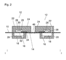
- FIG. 2 is a sectional view taking along the line II-II in FIG. 1 ;
- FIG. 3 is a plan view of a larger portion, on a reduced scale, of the substrate plate shown in FIG. 1 ;
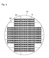
- FIG. 4 is a plan view of a substrate plate wafer for a plurality of MEMS devices.
- FIG. 5 is a plan view analogous to FIG. 1 , showing two MEMS devices after dicing.
- FIG. 1 a portion of a substrate plate 10 has been shown on which two MEMS devices 12 have been formed.
- a pattern 14 of electrically conductive leads is formed on one surface of the substrate plate 10 for contacting the electric components of the MEMS devices 12 .
- the MEMS devices 12 and the patterns 14 are arranged mirror-symmetrically in this example.
- each of the MEMS devices 12 constitutes a piezoelectric ink jet print head, which comprises a plurality of nozzles 16 .
- each of the nozzles 16 is connected to an ink chamber 18 that is formed in a chamber block 20 of the MEMS device 12 and is connected to an ink duct 22 via an opening formed in the substrate plate 10 .
- the ink duct 22 is formed in a duct block 24 that also forms an actuator chamber 26 accommodating a piezoelectric actuator 28 .
- the actuator 28 is bonded to the top surface of the substrate plate 10 .
- the substrate plate 10 forms a flexible membrane separating the ink chamber 18 from the actuator chamber 26 .
- the actuator 28 When energized, the actuator 28 deforms in a bending mode, thereby deflecting the flexible membrane so that the volume of the ink chamber 18 is changed and an acoustic pressure wave is generated.
- the acoustic pressure wave propagates through the ink in the ink chamber 18 towards the nozzle 16 , so that an ink droplet is ejected from the nozzle 18 .
- the actuator 28 is made of a thin film piezoelectric material, a ground electrode 30 and a signal electrode 32 .
- the actuator 28 is a multi-layer actuator comprising a number of parallel electrodes embedded in the piezoelectric material.
- the electrodes in this embodiment form an alternating sequence of ground electrodes and signal electrodes 32 .
- FIG. 2 only one ground electrode 30 on the top side of the actuator and one signal electrode 32 on the bottom side of the actuator have been shown.
- the signal electrode 32 is electrically connected to the conductive pattern 14 , which is formed on the bottom side of the substrate plate 10 in FIG. 2 .
- the ground electrodes 30 of each actuator are connected to other parts of the pattern 14 .
- each MEMS device 12 is arranged in three rows and, correspondingly, the actuators 28 are also arranged in respective rows. Connections between the electrodes 30 and 32 of each actuator and the pattern 14 are shown as dashed lines in FIG. 3 , because they are formed on the top side of the substrate plate 10 that is not visible in FIG. 3 .
- the pattern 14 is shown in greater detail in FIG. 1 and comprises, for each of the actuators 28 , a signal contact pad 36 that serves as a wire bonding pad and is connected to the signal electrode 32 by means of one of the vias 34 .
- a common ground contact pad 38 is connected, through another via 34 , to the ground electrodes 30 of the triplet of actuators 28 that occupy corresponding positions in the three nozzle rows.
- the ground contact pads 38 for the ground electrodes 30 of all actuators 28 on the MEMS device 12 are interconnected with each other (as is symbolized by a dashed line in FIG. 3 ) and are further connected to a device ground contact pad 40 disposed on one end (the left end in FIG. 1 ) of the nozzle row for grounding all actuators of the entire MEMS device.
- the signal and ground contact pads 36 , 38 for the first two actuator triplets shown in FIG. 1 have slightly different shapes. However, as is shown in FIG. 3 , the pattern is repeated periodically for the subsequent triplets.
- the signal electrodes 32 of all the actuators 28 must be isolated from one another.
- the signal contact pads 36 are all connected to a common lead structure 42 (a shunt bar) that extends along the border line of the two MEMS devices 12 .
- the lead structure 42 is connected to an extra contact pad 44 , which permits a common voltage to be applied to all of the signal electrodes 32 of all actuators 28 of both MEMS devices.
- Each of the plurality of chip-sized units includes a single MEMS device 12 .
- the lead structure 42 extends entirely inside the area of the dicing cut 48 .
- the width of the saw blade, and hence the width of the dicing cut 48 may be 70 ⁇ m, whereas the shunt lead structure 42 only has a width of 40 ⁇ m.
- the tolerance 70 ⁇ m as compared to 40 ⁇ m
- each of the signal contact pads 36 is connected to (and in some cases directly adjoins) a test pad 50 that may be used for applying test signals to the actuators 28 and/or for deriving test signals from the actuators 28 .
- the contour of the chamber blocks 20 of the two MEMS devices is shown in dashed lines. These contours delimit the footprint of the MEMS devices 12 on the substrate plate 10 .
- the test pads 50 are disposed within the footprint of the respective MEMS devices 12 , just as the signal contact pads 36 and the ground contact pads 38 .
- the extra contact pad 44 is also disposed (mainly) within the footprint of one of the MEMS devices 12 , so that only the lead structure 42 forming the shunt bar is disposed outside of the footprint of any MEMS device 12 .
- the test pads 50 may be used for applying and/or deriving test signals individually to and from each actuator 28 without having to use the contact pads 36 and 38 that may thus be reserved for wire bonding.
- FIG. 4 shows a plan view of a complete wafer-size substrate plate 10 on which a plurality of MEMS devices 12 are formed. Cut lines 52 along which the wafer will be diced in order to form the individual MEMS devices 12 have been shown schematically in FIG. 4 . Although not shown in FIG. 4 , it will be understood that the lead structures 42 may optionally be arranged to interconnect the lead patterns 14 for all the MEMS devices 12 on the wafer.
- FIG. 5 shows the MEMS devices 12 separated from one another after the dicing step, i.e. after the substrate plate 10 has been divided into chip-sized units 10 ′, also termed chips 10 ′. Comparing FIG. 5 to FIG. 1 , it can be seen that the lead structure 42 has been removed completely and the extra contact pad 44 is isolated from the signal and ground contact pads 36 , 38 , which are now also isolated from one another, with the signal contact pads 36 being still connected to their respective test pads 50 .
Landscapes
- Engineering & Computer Science (AREA)
- Manufacturing & Machinery (AREA)
- Microelectronics & Electronic Packaging (AREA)
- Physics & Mathematics (AREA)
- General Physics & Mathematics (AREA)
- Computer Hardware Design (AREA)
- Micromachines (AREA)
Applications Claiming Priority (3)
| Application Number | Priority Date | Filing Date | Title |
|---|---|---|---|
| EP13188352 | 2013-10-11 | ||
| EP13188352.2 | 2013-10-11 | ||
| EP13188352 | 2013-10-11 |
Publications (2)
| Publication Number | Publication Date |
|---|---|
| US20150102835A1 US20150102835A1 (en) | 2015-04-16 |
| US9856140B2 true US9856140B2 (en) | 2018-01-02 |
Family
ID=49326601
Family Applications (1)
| Application Number | Title | Priority Date | Filing Date |
|---|---|---|---|
| US14/512,105 Active 2035-03-01 US9856140B2 (en) | 2013-10-11 | 2014-10-10 | Substrate plate for MEMS devices |
Country Status (2)
| Country | Link |
|---|---|
| US (1) | US9856140B2 (de) |
| EP (1) | EP2860150B1 (de) |
Cited By (1)
| Publication number | Priority date | Publication date | Assignee | Title |
|---|---|---|---|---|
| US20200402918A1 (en) * | 2019-06-18 | 2020-12-24 | Nxp B.V. | Integrated Circuit Saw Bow Break Point |
Families Citing this family (15)
| Publication number | Priority date | Publication date | Assignee | Title |
|---|---|---|---|---|
| TWI620475B (zh) * | 2015-01-12 | 2018-04-01 | 南亞電路板股份有限公司 | 印刷電路板及其製作方法 |
| JP2017052135A (ja) * | 2015-09-08 | 2017-03-16 | セイコーエプソン株式会社 | Memsデバイス、液体噴射ヘッド、液体噴射装置、memsデバイスの製造方法、及び液体噴射ヘッドの製造方法 |
| JP6915327B2 (ja) * | 2017-03-17 | 2021-08-04 | 株式会社リコー | 液体吐出ヘッド、液体吐出ヘッドの製造方法、液体吐出ユニット、および液体を吐出する装置 |
| CN107580411B (zh) * | 2017-08-31 | 2019-12-24 | 广州兴森快捷电路科技有限公司 | 金手指引线结构及制作方法 |
| JP7031199B2 (ja) | 2017-09-27 | 2022-03-08 | ブラザー工業株式会社 | 圧電アクチュエータ、液体吐出ヘッド、及び、圧電アクチュエータの製造方法 |
| JP7077568B2 (ja) | 2017-09-29 | 2022-05-31 | ブラザー工業株式会社 | 液体吐出ヘッド |
| JP7047312B2 (ja) * | 2017-09-29 | 2022-04-05 | ブラザー工業株式会社 | 液体吐出ヘッド |
| JP7039914B2 (ja) | 2017-09-29 | 2022-03-23 | ブラザー工業株式会社 | 液体吐出ヘッド |
| CN111433036B (zh) * | 2017-12-08 | 2022-03-04 | 惠普发展公司,有限责任合伙企业 | 流体分配模具及其制造方法 |
| CN110146767A (zh) * | 2019-04-23 | 2019-08-20 | 江苏维尔兰电缆有限公司 | 一种用于检测承荷探测电缆导电性能的装置 |
| JP7459614B2 (ja) * | 2020-03-30 | 2024-04-02 | ブラザー工業株式会社 | 圧電アクチュエータ |
| JP7643004B2 (ja) * | 2020-09-28 | 2025-03-11 | ブラザー工業株式会社 | 圧電アクチュエータ及び圧電アクチュエータの検査方法 |
| JP7547898B2 (ja) | 2020-09-28 | 2024-09-10 | ブラザー工業株式会社 | 圧電アクチュエータ |
| CN113423170B (zh) * | 2021-06-17 | 2024-09-17 | 北京京东方光电科技有限公司 | 线路母板、线路板的制备方法 |
| ES2900841B2 (es) * | 2021-11-26 | 2023-03-02 | Kerajet S A | Dispositivo de impresion de inyeccion de tinta mems |
Citations (16)
| Publication number | Priority date | Publication date | Assignee | Title |
|---|---|---|---|---|
| US20010033183A1 (en) | 2000-04-25 | 2001-10-25 | Medtronic Inc. | Method and apparatus for wafer-level burn-in and testing of integrated circuits |
| US6624003B1 (en) * | 2002-02-06 | 2003-09-23 | Teravicta Technologies, Inc. | Integrated MEMS device and package |
| US20030211654A1 (en) | 2002-04-29 | 2003-11-13 | Texas Instruments Inc. | MEMS device wafer-level package |
| US20070143048A1 (en) | 2005-12-02 | 2007-06-21 | Semiconductor Energy Laboratory Co., Ltd. | Test method of microsctructure body and micromachine |
| US20090039489A1 (en) * | 2007-03-28 | 2009-02-12 | Albert Ting | method of producing optical mems |
| US20090160466A1 (en) * | 2007-12-24 | 2009-06-25 | Texas Instruments Incorporated | Self-isolating mixed design-rule integrated yeild monitor |
| US20090243645A1 (en) * | 2008-03-27 | 2009-10-01 | Renesas Technology Corp. | Manufacturing method of a semiconductor device, a semiconductor wafer, and a test method |
| US20090261476A1 (en) * | 2007-04-18 | 2009-10-22 | Siliconware Precision Industries Co., Ltd. | Semiconductor device and manufacturing method thereof |
| EP2290686A2 (de) | 2009-08-28 | 2011-03-02 | STMicroelectronics S.r.l. | Verfahren zum elektrischen Testen und zur Montage elektronischer Bauelemente |
| US20120080764A1 (en) * | 2010-09-30 | 2012-04-05 | Analog Devices, Inc. | Apparatus and method for microelectromechanical systems device packaging |
| US20120267730A1 (en) * | 2011-04-20 | 2012-10-25 | Tronics Microsystems S.A. | Micro-electromechanical system (mems) device |
| US20130082258A1 (en) | 2011-09-30 | 2013-04-04 | Stmicroelectronics Ltd (Malta) | Method for strip testing of mems devices, testing strip of mems devices and mems device thereof |
| US8633552B1 (en) * | 2007-03-01 | 2014-01-21 | Micrel, Incorporated | ESD protection for MEMS resonator devices |
| US20140210019A1 (en) * | 2013-01-30 | 2014-07-31 | Invensense, Inc. | Low-cost package for integrated mems sensors |
| US20140239423A1 (en) * | 2013-02-28 | 2014-08-28 | Lianjun Liu | Microelectromechanical system devices having through substrate vias and methods for the fabrication thereof |
| US9040360B1 (en) * | 2000-11-28 | 2015-05-26 | Knowles Electronics, Llc | Methods of manufacture of bottom port multi-part surface mount MEMS microphones |
-
2014
- 2014-10-08 EP EP14188211.8A patent/EP2860150B1/de not_active Not-in-force
- 2014-10-10 US US14/512,105 patent/US9856140B2/en active Active
Patent Citations (16)
| Publication number | Priority date | Publication date | Assignee | Title |
|---|---|---|---|---|
| US20010033183A1 (en) | 2000-04-25 | 2001-10-25 | Medtronic Inc. | Method and apparatus for wafer-level burn-in and testing of integrated circuits |
| US9040360B1 (en) * | 2000-11-28 | 2015-05-26 | Knowles Electronics, Llc | Methods of manufacture of bottom port multi-part surface mount MEMS microphones |
| US6624003B1 (en) * | 2002-02-06 | 2003-09-23 | Teravicta Technologies, Inc. | Integrated MEMS device and package |
| US20030211654A1 (en) | 2002-04-29 | 2003-11-13 | Texas Instruments Inc. | MEMS device wafer-level package |
| US20070143048A1 (en) | 2005-12-02 | 2007-06-21 | Semiconductor Energy Laboratory Co., Ltd. | Test method of microsctructure body and micromachine |
| US8633552B1 (en) * | 2007-03-01 | 2014-01-21 | Micrel, Incorporated | ESD protection for MEMS resonator devices |
| US20090039489A1 (en) * | 2007-03-28 | 2009-02-12 | Albert Ting | method of producing optical mems |
| US20090261476A1 (en) * | 2007-04-18 | 2009-10-22 | Siliconware Precision Industries Co., Ltd. | Semiconductor device and manufacturing method thereof |
| US20090160466A1 (en) * | 2007-12-24 | 2009-06-25 | Texas Instruments Incorporated | Self-isolating mixed design-rule integrated yeild monitor |
| US20090243645A1 (en) * | 2008-03-27 | 2009-10-01 | Renesas Technology Corp. | Manufacturing method of a semiconductor device, a semiconductor wafer, and a test method |
| EP2290686A2 (de) | 2009-08-28 | 2011-03-02 | STMicroelectronics S.r.l. | Verfahren zum elektrischen Testen und zur Montage elektronischer Bauelemente |
| US20120080764A1 (en) * | 2010-09-30 | 2012-04-05 | Analog Devices, Inc. | Apparatus and method for microelectromechanical systems device packaging |
| US20120267730A1 (en) * | 2011-04-20 | 2012-10-25 | Tronics Microsystems S.A. | Micro-electromechanical system (mems) device |
| US20130082258A1 (en) | 2011-09-30 | 2013-04-04 | Stmicroelectronics Ltd (Malta) | Method for strip testing of mems devices, testing strip of mems devices and mems device thereof |
| US20140210019A1 (en) * | 2013-01-30 | 2014-07-31 | Invensense, Inc. | Low-cost package for integrated mems sensors |
| US20140239423A1 (en) * | 2013-02-28 | 2014-08-28 | Lianjun Liu | Microelectromechanical system devices having through substrate vias and methods for the fabrication thereof |
Cited By (2)
| Publication number | Priority date | Publication date | Assignee | Title |
|---|---|---|---|---|
| US20200402918A1 (en) * | 2019-06-18 | 2020-12-24 | Nxp B.V. | Integrated Circuit Saw Bow Break Point |
| US10896878B2 (en) * | 2019-06-18 | 2021-01-19 | Nxp B.V. | Integrated circuit saw bow break point |
Also Published As
| Publication number | Publication date |
|---|---|
| US20150102835A1 (en) | 2015-04-16 |
| EP2860150A1 (de) | 2015-04-15 |
| EP2860150B1 (de) | 2021-01-06 |
Similar Documents
| Publication | Publication Date | Title |
|---|---|---|
| US9856140B2 (en) | Substrate plate for MEMS devices | |
| CN109148420B (zh) | 在半导体芯片制造过程期间防止esd | |
| US6696849B2 (en) | Fabrication method of semiconductor integrated circuit device and its testing apparatus | |
| KR102176584B1 (ko) | 정전용량 미세가공 초음파 변환기 및 그 제조방법 | |
| US8742564B2 (en) | Chip package and method for forming the same | |
| CN110114221B (zh) | Mems装置、液体喷射头、液体喷射装置以及它们的制造方法 | |
| CN103033699B (zh) | Mems器件、其条带测试方法及其测试条带 | |
| TW201320210A (zh) | 半導體裝置之製造方法、半導體裝置及配線形成用治具 | |
| EP1997638A1 (de) | Verfahren zur Erzeugung eines Arrays piezoelektrischer Aktuatoren auf einer Membran | |
| EP2965828A1 (de) | Kapazitive mikrobearbeitete ultraschallwandlersonde mittels drahtbonden | |
| TW201035572A (en) | Test device, test method, and production method | |
| JP6708412B2 (ja) | 液体吐出ヘッドおよびその製造方法 | |
| CN103848391A (zh) | 嵌入式芯片封装、芯片封装和制备嵌入式芯片封装的方法 | |
| US8393717B2 (en) | Liquid ejecting head and method of inspecting liquid ejecting head | |
| US20130147502A1 (en) | Vertical probe assembly with air channel | |
| CN101375384A (zh) | 包括不同器件的集成电路的制造 | |
| JP5646857B2 (ja) | ショートした流体吐出部の軽減 | |
| EP3199351A1 (de) | Tintenstrahlkopf und tintenstrahlkopfherstellungsverfahren | |
| TWM561908U (zh) | 晶粒功能檢測裝置 | |
| TW202215560A (zh) | 檢查用匣 | |
| JP2004288911A (ja) | 半導体ウエハ試験装置およびその試験方法 | |
| US11446927B2 (en) | Method of bonding printed circuit sheets | |
| CN114446921B (zh) | Mcm封装结构及其制作方法 | |
| CN114126772B (zh) | 板式换能器规模封装及其制造方法 | |
| JP4564423B2 (ja) | 半導体素子検査用基板の製造方法 |
Legal Events
| Date | Code | Title | Description |
|---|---|---|---|
| AS | Assignment |
Owner name: OCE-TECHNOLOGIES B.V., NETHERLANDS Free format text: ASSIGNMENT OF ASSIGNORS INTEREST;ASSIGNORS:HUYGENS, MAIKEL A.J.;VAN DER MEER, RENE J.;PANNEKOEK, REINIER;AND OTHERS;SIGNING DATES FROM 20141020 TO 20141127;REEL/FRAME:034482/0759 |
|
| STCF | Information on status: patent grant |
Free format text: PATENTED CASE |
|
| MAFP | Maintenance fee payment |
Free format text: PAYMENT OF MAINTENANCE FEE, 4TH YEAR, LARGE ENTITY (ORIGINAL EVENT CODE: M1551); ENTITY STATUS OF PATENT OWNER: LARGE ENTITY Year of fee payment: 4 |
|
| MAFP | Maintenance fee payment |
Free format text: PAYMENT OF MAINTENANCE FEE, 8TH YEAR, LARGE ENTITY (ORIGINAL EVENT CODE: M1552); ENTITY STATUS OF PATENT OWNER: LARGE ENTITY Year of fee payment: 8 |