US9831138B2 - Display substrate, method of testing the display substrate and display apparatus having the display substrate - Google Patents
Display substrate, method of testing the display substrate and display apparatus having the display substrate Download PDFInfo
- Publication number
- US9831138B2 US9831138B2 US14/290,064 US201414290064A US9831138B2 US 9831138 B2 US9831138 B2 US 9831138B2 US 201414290064 A US201414290064 A US 201414290064A US 9831138 B2 US9831138 B2 US 9831138B2
- Authority
- US
- United States
- Prior art keywords
- gate
- line
- gate clock
- sub pixel
- clock
- Prior art date
- Legal status (The legal status is an assumption and is not a legal conclusion. Google has not performed a legal analysis and makes no representation as to the accuracy of the status listed.)
- Active, expires
Links
Images


Classifications
-
- H—ELECTRICITY
- H01—ELECTRIC ELEMENTS
- H01L—SEMICONDUCTOR DEVICES NOT COVERED BY CLASS H10
- H01L22/00—Testing or measuring during manufacture or treatment; Reliability measurements, i.e. testing of parts without further processing to modify the parts as such; Structural arrangements therefor
- H01L22/30—Structural arrangements specially adapted for testing or measuring during manufacture or treatment, or specially adapted for reliability measurements
- H01L22/32—Additional lead-in metallisation on a device or substrate, e.g. additional pads or pad portions, lines in the scribe line, sacrificed conductors
-
- G—PHYSICS
- G09—EDUCATION; CRYPTOGRAPHY; DISPLAY; ADVERTISING; SEALS
- G09G—ARRANGEMENTS OR CIRCUITS FOR CONTROL OF INDICATING DEVICES USING STATIC MEANS TO PRESENT VARIABLE INFORMATION
- G09G3/00—Control arrangements or circuits, of interest only in connection with visual indicators other than cathode-ray tubes
- G09G3/006—Electronic inspection or testing of displays and display drivers, e.g. of LED or LCD displays
-
- G—PHYSICS
- G09—EDUCATION; CRYPTOGRAPHY; DISPLAY; ADVERTISING; SEALS
- G09G—ARRANGEMENTS OR CIRCUITS FOR CONTROL OF INDICATING DEVICES USING STATIC MEANS TO PRESENT VARIABLE INFORMATION
- G09G3/00—Control arrangements or circuits, of interest only in connection with visual indicators other than cathode-ray tubes
- G09G3/20—Control arrangements or circuits, of interest only in connection with visual indicators other than cathode-ray tubes for presentation of an assembly of a number of characters, e.g. a page, by composing the assembly by combination of individual elements arranged in a matrix no fixed position being assigned to or needed to be assigned to the individual characters or partial characters
- G09G3/34—Control arrangements or circuits, of interest only in connection with visual indicators other than cathode-ray tubes for presentation of an assembly of a number of characters, e.g. a page, by composing the assembly by combination of individual elements arranged in a matrix no fixed position being assigned to or needed to be assigned to the individual characters or partial characters by control of light from an independent source
- G09G3/36—Control arrangements or circuits, of interest only in connection with visual indicators other than cathode-ray tubes for presentation of an assembly of a number of characters, e.g. a page, by composing the assembly by combination of individual elements arranged in a matrix no fixed position being assigned to or needed to be assigned to the individual characters or partial characters by control of light from an independent source using liquid crystals
- G09G3/3611—Control of matrices with row and column drivers
- G09G3/3614—Control of polarity reversal in general
-
- G—PHYSICS
- G09—EDUCATION; CRYPTOGRAPHY; DISPLAY; ADVERTISING; SEALS
- G09G—ARRANGEMENTS OR CIRCUITS FOR CONTROL OF INDICATING DEVICES USING STATIC MEANS TO PRESENT VARIABLE INFORMATION
- G09G2300/00—Aspects of the constitution of display devices
- G09G2300/04—Structural and physical details of display devices
- G09G2300/0421—Structural details of the set of electrodes
- G09G2300/0426—Layout of electrodes and connections
Definitions
- Exemplary embodiments of the invention relate to a display substrate, a method of testing the display substrate and a display apparatus including the display substrate. More particularly, exemplary embodiments of the invention relate to a display substrate on which a test pad is provided, a method of testing the display substrate and a display apparatus including the display substrate.
- a display substrate of a display apparatus such as a liquid crystal display apparatus, includes a plurality of pixels.
- the pixels are typically disposed in a matrix form, and each of the pixels is electrically connected to a gate line and a data line.
- Each of the pixels may include a first sub pixel and a second sub pixel.
- a first pixel of the pixels may include the first sub pixel and the second sub pixel
- a second pixel of the pixels, which is adjacent to the first pixel may include the first sub pixel and the second sub pixel.
- Data signals having different polarities may be respectively charged to the first sub pixel and the second sub pixel.
- a data voltage of the second sub pixel in the first pixel and the first sub pixel in the second pixel becomes a reference voltage (e.g., about zero volt), defining the polarities of the data signals, when a short between the first pixel and the second pixel occurs, such that short between the first pixel and the second pixel may be effectively detected based on whether the data voltage of the second sub pixel in the first pixel and the first sub pixel in the second pixel is the reference voltage (e.g., about zero volt) or not.
- the data voltage at a point where the second sub pixel in the first pixel and the first sub pixel in the second pixel are short is not the reference voltage or about zero, such that the short between the first pixel and the second pixel may not be effectively detected based on whether the data voltage of the second sub pixel in the first pixel and the first sub pixel in the second pixel is the reference voltage (e.g., about zero volt) or not.
- Exemplary embodiments of the invention provide a display substrate with improved or increased defect detection ratio of the display substrate.
- Exemplary embodiments of the invention also provide a method of testing the above-mentioned display substrate.
- Exemplary embodiments of the invention also provide a display apparatus including the above-mentioned display substrate.
- a display substrate includes a first gate line, a second gate line, a first data line, a second data line, a first pixel, a second pixel, a first pad and a second pad.
- the first gate line is configured to receive a first gate clock
- the second gate line is adjacent to the first gate line and is configured to receive a second gate clock
- the first data line is configured to transfer a first data signal inverted according to the first gate clock and the second gate clock
- the first data signal has a first polarity
- the second data line is configured to transfer a second data signal inverted according to the first gate clock and the second gate clock
- the second data signal has a second polarity different from the first polarity.
- the first pixel includes a first high sub pixel electrically connected to the first gate line and the first data line, and a first low sub pixel electrically connected to the first gate line and the second data line
- the second pixel includes a second high sub pixel electrically connected to the second gate line and the second data line, and a second low sub pixel electrically connected to the second gate line and the first data line.
- the first pad is configured to output the first gate clock to the first gate line
- the second pad is configured to output the second gate clock to the second gate line.
- the first data signal when the first pad outputs the first gate clock, the first data signal may have a positive polarity and the second data signal may have a negative polarity, and when the second pad outputs the second gate clock, the first data signal may have the negative polarity and the second data signal may have the positive polarity.
- the first data signal when the first pad outputs the first gate clock, the first data signal may have a negative polarity and the second data signal may have a positive polarity, and when the second pad outputs the second gate clock, the first data signal may have the positive polarity and the second data signal may have the negative polarity.
- the second gate clock may be activated after the first gate clock is activated and deactivated.
- the display substrate may further include a third gate line and a third pixel.
- the third gate line may be adjacent to the second gate line and may be configured to receive the first gate clock
- the third pixel may include a third high sub pixel electrically connected to the third gate line and the first data line, and a third low pixel electrically connected to the third gate line and the second data line.
- the display substrate may further include a third pad configured to output the first gate clock to the third gate line.
- the first pad and the third pad may be electrically connected to each other.
- the first pad may be configured to further output the first gate clock to the third gate line.
- the display substrate may further include a fourth gate line, a fourth pixel and a fourth pad.
- the fourth gate line may be adjacent to the third gate line and may be configured to receive the second gate clock
- the fourth pixel may include a fourth high sub pixel electrically connected to the fourth gate line and the second data line, and a fourth low sub pixel electrically connected to the fourth gate line and the first data line
- the fourth pad may be configured to output the second gate clock to the fourth gate line.
- the second gate clock may include a positive second gate clock and a negative second gate clock
- the second pad may be configured to output the positive second gate clock
- the fourth pad may be configured to output the negative second gate clock
- the display substrate may further include a fifth gate line, a fifth pixel and a fifth pad.
- the fifth gate line may be adjacent to the fourth gate line and may be configured to receive the first gate clock
- the fifth pixel may include a fifth high sub pixel electrically connected to the fifth gate line and the first data line, and a fifth low sub pixel electrically connected to the fifth gate line and the second data line
- the fifth pad may be configured to output the first gate clock to the fifth gate line.
- the first gate clock may include a positive first gate clock and a negative first gate clock
- the first pad may be configured to output the positive first gate clock
- the fifth pad may be configured to output the negative second gate clock
- the display substrate may further include a sixth gate line and a sixth pixel.
- the sixth gate line may be adjacent to the fifth gate line and may be configured to receive the second gate clock
- the sixth pixel may include a sixth high sub pixel electrically connected to the sixth gate line and the second data line, and a sixth low sub pixel electrically connected to the sixth gate line and the first data line.
- the display substrate may further include a sixth pad may be configured to output the second gate clock to the sixth gate line.
- the fourth pad and the sixth pad may be electrically connected to each other.
- the fourth pad may be configured to further output the second gate clock to the sixth gate line.
- a method of testing a display substrate includes: applying a first gate clock to a first gate line of the display substrate, where the display substrate includes the first gate line configured to receive the first gate clock, a second gate line adjacent to the first gate line and configured to receive a second gate clock, a first data line configured to transfer a first data signal inverted according to the first gate clock and the second gate clock, a second data line configured to transfer a second data signal inverted according to the first gate clock and the second gate clock, a first pixel including a first high sub pixel electrically connected to the first gate line and the first data line and a first low sub pixel electrically connected to the first gate line and the second data line, and a second pixel including a second high sub pixel electrically connected to the second gate line and the second data line and a second low sub pixel electrically connected to the second gate line and the first data line; applying the first data signal and the second data signal to the first data line and the second data line, applying the second gate clock to the first data line and the second data line,
- the first gate clock may include a positive first gate clock and a negative first gate clock.
- the second gate clock may include a positive second gate clock and a negative second gate clock.
- a display apparatus includes a display substrate, a gate driving part and a data driving part.
- the display substrate includes a first gate line configured to receive a first gate clock, a second gate line adjacent to the first gate line and configured to receive a second gate clock, a first data line configured to transfer a first data signal inverted according to the first gate clock and the second gate clock, a second data line configured to transfer a second data signal inverted according to the first gate clock and the second gate clock, a first pixel including a first high sub pixel electrically connected to the first gate line and the first data line and a first low sub pixel electrically connected to the first gate line and the second data line, a second pixel including a second high sub pixel electrically connected to the second gate line and the second data line and a second low sub pixel electrically connected to the second gate line and the first data line, a first pad configured to output the first gate clock to the first gate line, and a second pad configured to output the second gate clock
- polarities of high sub pixels adjacent in a first direction are different from each other
- polarities of low sub pixels adjacent in the first direction are different from each other
- polarities of the low sub pixel and the high sub pixel adjacent in the second direction are different from each other, such that a short between the pixels may be effectively detected based on detecting a point having the reference voltage in adjacent pixels.
- defect detection ratio of the display substrate may be increased.
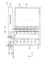
- FIG. 1A is a plan view illustrating an exemplary embodiment of a display substrate according to the invention.
- FIGS. 1B and 1C are circuit diagrams showing sub-pixels of a pixel of the display substrate shown in FIG. 1A ;
- FIG. 2 is a signal timing diagram of a positive first gate clock, the positive second gate clock, a negative first gate clock and a negative second gate clock of FIG. 1A ;
- FIG. 3A is a plan view illustrating first to twelfth pixels of FIG. 1A , when the positive first gate clock, the positive first gate clock and the negative first gate clock are respectively applied to a first gate line, a third gate line and a fifth gate line;
- FIG. 3B is a plan view illustrating the first to twelfth pixels of FIG. 1A , when the positive second gate clock, the negative second gate clock and the negative second gate clock are respectively applied to a second gate line, a fourth gate line and a sixth gate line;
- FIG. 3C is a plan view illustrating the first to twelfth pixels of FIG. 1A , when the positive first gate clock, the positive first gate clock, the negative first gate clock, the positive second gate clock, the negative second gate clock and the negative second gate clock are respectively applied to the first gate line, the third gate line, the fifth gate line, the second gate line, the fourth gate line and the sixth gate line;
- FIG. 4 is a flow chart illustrating an exemplary embodiment of a method of testing the display substrate of FIG. 1A ;
- FIG. 5 is a block diagram illustrating an exemplary embodiment of a display apparatus including the display substrate of FIG. 1A ;
- FIG. 6A is a plan view illustrating first to twelfth pixels of an exemplary embodiment of a display substrate, when a positive first gate clock, the positive first gate clock and a negative first gate clock are respectively applied to a first gate line, a third gate line and a fifth gate line, according to the invention;
- FIG. 6B is a plan view illustrating the first to twelfth pixels of an exemplary embodiment of a display substrate, when the positive second gate clock, the negative second gate clock and the negative second gate clock are respectively applied to the second gate line, the fourth gate line and the sixth gate line, according to the invention;
- FIG. 6C is a plan view illustrating the first to twelfth pixels of an exemplary embodiment of a display substrate, when the positive first gate clock, the positive first gate clock, the negative first gate clock, the positive second gate clock, the negative second gate clock and the negative second gate clock are respectively applied to the first gate line, the third gate line, the fifth gate line, the second gate line, the fourth gate line and the sixth gate line, according to the invention;
- FIG. 7A is a plan view illustrating an alternative exemplary embodiment of a display substrate according to the invention.
- FIGS. 7B and 7C are circuit diagrams showing sub-pixels of a pixel of the display substrate shown in FIG. 7A
- FIG. 8 is a block diagram illustrating an exemplary embodiment of a display apparatus including the display substrate of FIG. 7A ;
- FIG. 9A is a plan view illustrating another alternative exemplary embodiment of a display substrate according to the invention.
- FIGS. 9B and 9C are circuit diagrams showing sub-pixels of a pixel of the display substrate shown in FIG. 9A ;
- FIG. 10 is a block diagram illustrating an exemplary embodiment of a display apparatus including the display substrate of FIG. 9A .
- first,” “second,” “third” etc. may be used herein to describe various elements, components, regions, layers and/or sections, these elements, components, regions, layers and/or sections should not be limited by these terms. These terms are only used to distinguish one element, component, region, layer or section from another element, component, region, layer or section. Thus, “a first element,” “component,” “region,” “layer” or “section” discussed below could be termed a second element, component, region, layer or section without departing from the teachings herein.
- relative terms such as “lower” or “bottom” and “upper” or “top,” may be used herein to describe one element's relationship to another element as illustrated in the Figures. It will be understood that relative terms are intended to encompass different orientations of the device in addition to the orientation depicted in the Figures. For example, if the device in one of the figures is turned over, elements described as being on the “lower” side of other elements would then be oriented on “upper” sides of the other elements. The exemplary term “lower,” can therefore, encompasses both an orientation of “lower” and “upper,” depending on the particular orientation of the figure.
- “About” or “approximately” as used herein is inclusive of the stated value and means within an acceptable range of deviation for the particular value as determined by one of ordinary skill in the art, considering the measurement in question and the error associated with measurement of the particular quantity (i.e., the limitations of the measurement system). For example, “about” can mean within one or more standard deviations, or within ⁇ 30%, 20%, 10%, 5% of the stated value.
- Exemplary embodiments are described herein with reference to cross section illustrations that are schematic illustrations of idealized embodiments. As such, variations from the shapes of the illustrations as a result, for example, of manufacturing techniques and/or tolerances, are to be expected. Thus, embodiments described herein should not be construed as limited to the particular shapes of regions as illustrated herein but are to include deviations in shapes that result, for example, from manufacturing. For example, a region illustrated or described as flat may, typically, have rough and/or nonlinear features. Moreover, sharp angles that are illustrated may be rounded. Thus, the regions illustrated in the figures are schematic in nature and their shapes are not intended to illustrate the precise shape of a region and are not intended to limit the scope of the claims.
- FIG. 1A is a plan view illustrating an exemplary embodiment of a display substrate according to the invention
- FIGS. 1B and 1C are circuit diagrams showing sub-pixels of a pixel of the display substrate shown in FIG. 1A .
- an exemplary embodiment of the display substrate 100 includes an array portion 200 and a pad portion 300 .
- the array portion 200 includes gate lines, data lines and a plurality of pixels disposed substantially in a matrix form.
- the array portion 200 may include first gate line GL 1 , a second gate line GL 2 , a third gate line GL 3 , a fourth gate line GL 4 , a fifth gate line GL 5 and a sixth gate line GL 6 .
- the array portion 200 may include a first data line DL 1 , a second data line DL 2 , a third data line DL 3 and a fourth data line DL 4 .
- the array portion 200 may include a first pixel 201 , a second pixel 202 , a third pixel 203 , a fourth pixel 204 , a fifth pixel 205 , a sixth pixel 206 , a seventh pixel 207 , an eighth pixel 208 , a ninth pixel 209 , a tenth pixel 210 , an eleventh pixel 211 and a twelfth pixel 212 .
- the first to sixth gate lines GL 1 , GL 2 , . . . , GL 6 extend substantially in a first direction D 1 .
- the first to fourth data lines DL 1 , DL 2 , . . . , DL 4 extend substantially in a second direction, which is perpendicular to the first direction D 1 .
- the first data line DL 1 transfers a first data signal
- the second data line DL 2 transfers a second data signal
- the third data line DL 3 transfers a third data signal
- the fourth data line DL 4 transfers a fourth data signal.
- polarities of data signals applied to adjacent data lines are different from each other.
- a polarity of the first data signal and a polarity of the second data signal is different from each other
- the polarity of the second data signal and a polarity of the third data signal is different from each other
- the polarity of the third data signal and a polarity of the fourth data signal is different from each other.
- the second data line DL 2 and the third data line DL 3 are disposed between the first pixel 201 and the seventh pixel 207 , between the second pixel 202 and the eighth pixel 208 , between the third pixel 203 and the ninth pixel 209 , between the fourth pixel 204 and the tenth pixel 210 , between the fifth pixel 205 and the eleventh pixel 211 , and between the sixth pixel 206 and the twelfth pixel 212 .
- the first direction D 1 may be substantially parallel to a long side of the display substrate 100
- the second direction D 2 may be substantially parallel to a short side of the display substrate 100 .
- the first pixel 201 includes a first high sub pixel 201 a and a first low sub pixel 201 b .
- the first high sub pixel 201 a is electrically connected to the first gate line GL 1 and the first data line DL 1 .
- the first high sub pixel 201 a includes a first thin film transistor 221 electrically connected to the first gate line GL 1 and the first data line DL 1 , a first liquid crystal capacitor 222 and a first storage capacitor 223 , which are electrically connected to the first thin film transistor 221 .
- the first low sub pixel 201 b is electrically connected to the first gate line GL 1 and the second data line DL 2 .
- the first low sub pixel 201 b includes a second thin film transistor 231 electrically connected to the first gate line GL 1 and the second data line DL 2 , a second liquid crystal capacitor 232 and a second storage capacitor 233 , which are electrically connected to the second thin film transistor 231 .
- the second pixel 202 includes a second high sub pixel 202 a and a second low sub pixel 202 b .
- the second high sub pixel 202 a is electrically connected to the second gate line GL 2 and the second data line DL 2 .
- a structure of the second high sub pixel 202 a is substantially the same as a structure of the first high sub pixel 201 a .
- the second low sub pixel 202 b is electrically connected to the second gate line GL 2 and the first data line DL 1 .
- a structure of the second low sub pixel 202 b is substantially the same as a structure of the first low sub pixel 201 b.
- the third pixel 203 includes a third high sub pixel 203 a and a third low sub pixel 203 b .
- the third high sub pixel 203 a is electrically connected to the third gate line GL 3 and the first data line DL 1 .
- a structure of the third high sub pixel 203 a is substantially the same as the structure of the first high sub pixel 201 a .
- the third low sub pixel 203 b is electrically connected to the third gate line GL 3 and the second data line DL 2 .
- a structure of the third low sub pixel 203 b is substantially the same as the structure of the first low sub pixel 201 b.
- the fourth pixel 204 includes a fourth high sub pixel 204 a and a fourth low sub pixel 204 b .
- the fourth high sub pixel 204 a is electrically connected to the fourth gate line GL 4 and the second data line DL 2 .
- a structure of the fourth high sub pixel 204 a is substantially the same as the structure of the first high sub pixel 201 a .
- the fourth low sub pixel 204 b is electrically connected to the fourth gate line GL 4 and the first data line DL 1 .
- a structure of the fourth low sub pixel 204 b is substantially the same as the structure of the first low sub pixel 201 b.
- the fifth pixel 205 includes a fifth high sub pixel 205 a and a fifth low sub pixel 205 b .
- the fifth high sub pixel 205 a is electrically connected to the fifth gate line GL 5 and the first data line DL 1 .
- a structure of the fifth high sub pixel 205 a is substantially the same as the structure of the first high sub pixel 201 a .
- the fifth low sub pixel 205 b is electrically connected to the fifth gate line GL 5 and the second data line DL 2 .
- a structure of the fifth low sub pixel 205 b is substantially the same as the structure of the first low sub pixel 201 b.
- the sixth pixel 206 includes a sixth high sub pixel 206 a and a sixth low sub pixel 206 b .
- the sixth high sub pixel 206 a is electrically connected to the sixth gate line GL 6 and the second data line DL 2 .
- a structure of the sixth high sub pixel 206 a is substantially the same as the structure of the first high sub pixel 201 a .
- the sixth low sub pixel 206 b is electrically connected to the sixth gate line GL 6 and the first data line DL 1 .
- a structure of the sixth low sub pixel 206 b is substantially the same as the structure of the first low sub pixel 201 b.
- the seventh pixel 207 includes a seventh high sub pixel 207 a and a seventh low sub pixel 207 b .
- the seventh high sub pixel 207 a is electrically connected to the first gate line GL 1 and the fourth data line DL 4 .
- a structure of the seventh high sub pixel 207 a is substantially the same as the structure of the first high sub pixel 201 a .
- the seventh low sub pixel 207 b is electrically connected to the first gate line GL 1 and the third data line DL 3 .
- a structure of the seventh low sub pixel 207 b is substantially the same as the structure of the first low sub pixel 201 b.
- the eighth pixel 208 includes an eighth high sub pixel 208 a and an eighth low sub pixel 208 b .
- the eighth high sub pixel 208 a is electrically connected to the second gate line GL 2 and the third data line DL 3 .
- a structure of the eighth high sub pixel 208 a is substantially the same as the structure of the first high sub pixel 201 a .
- the eighth low sub pixel 208 b is electrically connected to the second gate line GL 2 and the fourth data line DL 4 .
- a structure of the eighth low sub pixel 208 b is substantially the same as the structure of the first low sub pixel 201 b.
- the ninth pixel 209 includes a ninth high sub pixel 209 a and a ninth low sub pixel 209 b .
- the ninth high sub pixel 209 a is electrically connected to the third gate line GL 3 and the fourth data line DL 4 .
- a structure of the ninth high sub pixel 209 a is substantially the same as the structure of the first high sub pixel 201 a .
- the ninth low sub pixel 209 b is electrically connected to the third gate line GL 3 and the third data line DL 3 .
- a structure of the ninth low sub pixel 209 b is substantially the same as the structure of the first low sub pixel 201 b.
- the tenth pixel 210 includes a tenth high sub pixel 210 a and a tenth low sub pixel 210 b .
- the tenth high sub pixel 210 a is electrically connected to the fourth gate line GL 4 and the third data line DL 3 .
- a structure of the tenth high sub pixel 210 a is substantially the same as the structure of the first high sub pixel 201 a .
- the tenth low sub pixel 210 b is electrically connected to the fourth gate line GL 4 and the fourth data line DL 4 .
- a structure of the tenth low sub pixel 210 b is substantially the same as the structure of the first low sub pixel 201 b.
- the eleventh pixel 211 includes an eleventh high sub pixel 211 a and an eleventh low sub pixel 211 b .
- the eleventh high sub pixel 211 a is electrically connected to the fifth gate line GL 5 and the fourth data line DL 4 .
- a structure of the eleventh high sub pixel 211 a is substantially the same as the structure of the first high sub pixel 201 a .
- the eleventh low sub pixel 211 b is electrically connected to the fifth gate line GL 5 and the third data line DL 3 .
- a structure of the eleventh low sub pixel 211 b is substantially the same as the structure of the first low sub pixel 201 b.
- the twelfth pixel 212 includes a twelfth high sub pixel 212 a and a twelfth low sub pixel 212 b .
- the twelfth high sub pixel 212 a is electrically connected to the sixth gate line GL 6 and the third data line DL 3 .
- a structure of the twelfth high sub pixel 212 a is substantially the same as the structure of the first high sub pixel 201 a .
- the twelfth low sub pixel 212 b is electrically connected to the sixth gate line GL 6 and the fourth data line DL 4 .
- a structure of the twelfth low sub pixel 212 b is substantially the same as the structure of the first low sub pixel 201 b.
- the structure defined by the first to sixth gate lines GL 1 , GL 2 , . . . , GL 6 , the first to fourth data lines DL 1 , DL 2 , . . . , DL 4 and the first to twelfth pixels 201 , 202 , . . . , 212 may be repeatedly disposed in the array portion 200 in first direction D 1 and the second direction D 2 .
- the pad portion 300 includes a first pad 310 , a second pad 320 , a third pad 330 , a fourth pad 340 , a fifth pad 350 and a sixth pad 360 .
- the first pad 310 outputs a positive first gate clock +GCK 1 to the first gate line GL 1 .
- the first pad 310 may receive the positive first gate clock +GCK 1 from an outside (e.g., an external device) to output the positive first gate clock +GCK 1 to the first gate line GL 1 .
- the second pad 320 outputs a positive second gate clock +GCK 2 to the second gate line GL 2 .
- the second pad 320 may receive the positive second gate clock +GCK 2 from the outside to output the positive second gate clock +GCK 2 to the second gate line GL 2 .
- the third pad 330 is electrically connected to the first pad 310 , and outputs the positive first gate clock +GCK 1 to the third gate line GL 3 .
- the third pad 330 may receive the positive first gate clock +GCK 1 from the outside to output the positive first gate clock +GCK 1 to the third gate line GL 3 .
- the third pad 330 may receive the positive first gate clock +GCK 1 from the first pad 310 to output the positive first gate clock +GCK 1 to the third gate line GL 3 .
- the first pad 310 and the third pad 330 are electrically connected to each other as shown in FIG. 1A , but not being limited thereto.
- the first pad 310 and the third pad 330 may be formed with or defined by a same pad.
- the fourth pad 340 outputs a negative second gate clock ⁇ GCK 2 to the fourth gate line GL 4 .
- the fourth pad 340 may receive the negative second gate clock ⁇ GCK 2 from the outside to output the negative second gate clock ⁇ GCK 2 to the fourth gate line GL 4 .
- the fifth pad 350 outputs a negative first gate clock ⁇ GCK 1 to the fifth gate line GL 5 .
- the fifth pad 350 may receive the negative first gate clock ⁇ GCK 1 from the outside to output the negative first gate clock ⁇ GCK 1 to the fifth gate line GL 5 .
- the sixth pad 360 is electrically connected to the fourth pad 340 , and outputs the negative second gate clock ⁇ GCK 2 to the sixth gate line GL 6 .
- the sixth pad 360 may receive the negative second gate clock ⁇ GCK 2 from the outside to output the negative second gate clock ⁇ GCK 2 to the sixth gate line GL 6 .
- the sixth pad 360 may receive the negative second gate clock ⁇ GCK 2 from the fourth pad 340 to output the negative second gate clock ⁇ GCK 2 to the sixth gate line GL 6 .
- the fourth pad 340 and the sixth pad 360 are electrically connected to each other as shown in FIG. 1A , but not being limited thereto.
- the fourth pad 340 and the sixth pad 360 may be formed with or defined by a same pad.
- the positive first gate clock +GCK 1 , the positive second gate clock +GCK 2 , the negative first gate clock ⁇ GCK 1 and the negative second gate clock ⁇ GCK 2 may be test signals for testing the first to twelfth pixels 201 , 202 , . . . , 212 in the array portion 200 .
- FIG. 2 is a signal timing diagram of the positive first gate clock +GCK 1 , the positive second gate clock +GCK 2 , the negative first gate clock ⁇ GCK 1 and the negative second gate clock ⁇ GCK 2 of FIG. 1A .
- the positive second gate clock +GCK 2 and the negative second gate clock ⁇ GCK 2 are activated, e.g., in a high level, after the positive first gate clock +GCK 1 and the negative first gate clock ⁇ GCK 1 are activated.
- the positive first gate clock +GCK 1 and the negative first gate clock ⁇ GCK 1 are simultaneously activated, and the positive second gate clock +GCK 2 and the negative second gate clock ⁇ GCK 2 are activated after the positive first gate clock +GCK 1 and the negative first gate clock ⁇ GCK 1 are deactivated, e.g., in a low level.
- the negative first gate clock ⁇ GCK 1 is inverted to the positive first gate clock +GCK 1
- the negative second gate clock ⁇ GCK 2 is inverted to the positive second gate clock +GCK 2
- polarities of the first to fourth data signals transferred through the first to fourth data lines DL 1 , DL 2 , . . . , DL 4 of FIG. 1A when the positive second gate clock +GCK 2 and the negative second gate clock ⁇ GCK 2 are activated are opposite to polarities of the first to fourth data signals transferred through the first to fourth data lines DL 1 , DL 2 , . . . , DL 4 of FIG. 1A when the positive first gate clock +GCK 1 and the negative first gate clock ⁇ GCK 1 are activated.
- FIG. 3A is a plan view illustrating the first to twelfth pixels 201 , 202 , . . . , 212 of FIG. 1A , when the positive first gate clock +GCK 1 , the positive first gate clock +GCK 1 and the negative first gate clock ⁇ GCK 1 are respectively applied to the first gate line GL 1 , the third gate line GL 3 and the fifth gate line GL 5 .
- the first data signal applied to the first data line DL 1 may have a positive polarity
- the second data signal applied to the second data line DL 2 may have a negative polarity
- the third data signal applied to the third data line DL 3 may have the positive polarity
- the fourth data signal applied to the fourth data line DL 4 may have the negative polarity.
- the positive polarity and the negative polarity may be defined with reference to a reference voltage.
- the data signal has the positive polarity when the data signal is greater than the reference voltage, and the data signal has the negative polarity when the data signal is less than the reference voltage.
- the reference voltage may be about zero (0) volt.
- the reference voltage may be a common voltage.
- the positive first gate clock +GCK 1 , the positive first gate clock +GCK 1 and the negative first gate clock ⁇ GCK 1 are respectively applied to the first gate line GL 1 , the third gate line GL 3 and the fifth gate line GL 5 , a data voltage having the positive polarity is charged to each of the first high sub pixel 201 a , the third high sub pixel 203 a , the fifth high sub pixel 205 a , the seventh low sub pixel 207 b , the ninth low sub pixel 209 b and the eleventh low sub pixel 211 b .
- the positive first gate clock +GCK 1 , the positive first gate clock +GCK 1 and the negative first gate clock ⁇ GCK 1 are respectively applied to the first gate line GL 1 , the third gate line GL 3 and the fifth gate line GL 5 , a data voltage having the negative polarity is charged to each of the first low sub pixel 201 b , the third low sub pixel 203 b , the fifth low sub pixel 205 b , the seventh high sub pixel 207 a , the ninth high sub pixel 209 b and the eleventh high sub pixel 211 a.
- FIG. 3B is a plan view illustrating the first to twelfth pixels 201 , 202 , . . . , 212 of FIG. 1A , when the positive second gate clock +GCK 2 , the negative second gate clock ⁇ GCK 2 and the negative second gate clock ⁇ GCK 2 are respectively applied to the second gate line GL 2 , the fourth gate line GL 4 and the sixth gate line GL 6 .
- the first data signal applied to the first data line DL 1 may have the negative polarity
- the second data signal applied to the second data line DL 2 may have the positive polarity
- the third data signal applied to the third data line DL 3 may have the negative polarity
- the fourth data signal applied to the fourth data line DL 4 may have the positive polarity.
- the data voltage having the positive polarity is charged to each of the second high sub pixel 202 a , the fourth high sub pixel 204 a , the sixth high sub pixel 206 a , the eighth low sub pixel 208 b , the tenth low sub pixel 210 b and the twelfth low sub pixel 212 b .
- the data voltage having the negative polarity is charged to each of the second low sub pixel 202 b , the fourth low sub pixel 204 b , the sixth low sub pixel 206 b , the eighth high sub pixel 208 a , the tenth high sub pixel 210 a and the twelfth high sub pixel 212 a.
- FIG. 3C is a plan view illustrating the first to twelfth pixels 201 , 202 , . . . , 212 of FIG. 1A , when the positive first gate clock +GCK 1 , the positive first gate clock +GCK 1 , the negative first gate clock ⁇ GCK 1 , the positive second gate clock +GCK 2 , the negative second gate clock ⁇ GCK 2 and the negative second gate clock ⁇ GCK 2 are respectively applied to the first gate line GL 1 , the third gate line GL 3 , the fifth gate line GL 5 , the second gate line GL 2 , the fourth gate line GL 4 and the sixth gate line GL 6 .
- polarities of high sub pixels adjacent in the first direction D 1 are different from each other.
- the first high sub pixel 201 a has the positive polarity and the seventh high sub pixel 207 a has the negative polarity.
- polarities of low sub pixels adjacent in the first direction D 1 are different from each other.
- the first low sub pixel 201 b has the negative polarity and the seventh low sub pixel 207 b has the positive polarity.
- polarities of a low sub pixel and a high sub pixel adjacent in the second direction D 2 are different from each other.
- the first low sub pixel 201 b has the negative polarity and the second high sub pixel 202 a has the positive polarity.
- FIG. 4 is a flow chart illustrating an exemplary embodiment of a method of testing the display substrate 100 of FIG. 1A .
- the first gate clocks are applied (S 110 ).
- the first gate clocks include the positive first gate clock +GCK 1 and the negative first gate clock ⁇ GCK 1 .
- the positive first gate clock +GCK 1 is applied from the first pad 310 to the first gate line GL 1
- the positive first gate clock +GCK 1 is applied from the third pad 330 to the third gate line GL 3
- the negative first gate clock ⁇ GCK 1 is applied from the fifth pad 350 to the fifth gate line GL 5 for testing the pixels in the array portion 200 .
- the data signals are applied (S 120 ).
- the positive first gate clock +GCK 1 , the positive first gate clock +GCK 1 and the negative first gate clock ⁇ GCK 1 are respectively applied to the first gate line GL 1 , the third gate line GL 3 and the fifth gate line GL 5 for testing the pixels in the array portion 200
- the first data signal applied to the first data line DL 1 may have the positive polarity
- the second data signal applied to the second data line DL 2 may have the negative polarity
- the third data signal applied to the third data line DL 3 may have the positive polarity
- the fourth data signal applied to the fourth data line DL 4 may have the negative polarity.
- the data voltage having the positive polarity is charged to each of the first high sub pixel 201 a , the third high sub pixel 203 a , the fifth high sub pixel 205 a , the seventh low sub pixel 207 b , the ninth low sub pixel 209 b and the eleventh low sub pixel 211 b .
- the data voltage having the negative polarity is charged to each of the first low sub pixel 201 b , the third low sub pixel 203 b , the fifth low sub pixel 205 b , the seventh high sub pixel 207 a , the ninth high sub pixel 209 b and the eleventh high sub pixel 211 a.
- the second gate clocks are applied (S 130 ).
- the second gate clocks include the positive second gate clock +GCK 2 and the negative second gate clock ⁇ GCK 2 .
- the positive second gate clock +GCK 2 is applied from the second pad 320 to the second gate line GL 2
- the negative second gate clock ⁇ GCK 2 is applied from the fourth pad 340 to the fourth gate line GL 4
- the negative second gate clock ⁇ GCK 2 is applied from the sixth pad 360 to the sixth gate line GL 6 .
- the data signals are applied (S 140 ).
- the positive second gate clock +GCK 2 , the negative second gate clock ⁇ GCK 2 and the negative second gate clock ⁇ GCK 2 are respectively applied to the second gate line GL 2 , the fourth gate line GL 4 and the sixth gate line GL 6 for testing the pixels in the array portion 200
- the first data signal applied to the first data line DL 1 may have the negative polarity
- the second data signal applied to the second data line DL 2 may have the positive polarity
- the third data signal applied to the third data line DL 3 may have the negative polarity
- the fourth data signal applied to the fourth data line DL 4 may have the positive polarity.
- the data voltage having the positive polarity is charged to each of the second high sub pixel 202 a , the fourth high sub pixel 204 a , the sixth high sub pixel 206 a , the eighth low sub pixel 208 b , the tenth low sub pixel 210 b and the twelfth low sub pixel 212 b .
- the data voltage having the negative polarity is charged to each of the second low sub pixel 202 b , the fourth low sub pixel 204 b , the sixth low sub pixel 206 b , the eighth high sub pixel 208 a , the tenth high sub pixel 210 a and the twelfth high sub pixel 212 a.
- the adjacent pixels are short or not (S 150 ).
- whether the adjacent pixels are short or not may be determined by detecting a point having the reference voltage in the adjacent pixels.
- the polarities of the high sub pixels adjacent in the first direction D 1 are different from each other. Therefore, when the high sub pixels adjacent in the first direction D 1 are short, the reference voltage defining the positive polarity and the negative polarity is detected at a point where the adjacent high sub pixels are short.
- the polarities of the low sub pixels adjacent in the first direction D 1 are different from each other.
- the reference voltage defining the positive polarity and the negative polarity is detected at a point where the adjacent low sub pixels are short.
- the polarities of the low sub pixel and the high sub pixel adjacent in the second direction D 2 are different from each other. Therefore, when the low sub pixel and the high sub pixel adjacent in the second direction D 2 are short, the reference voltage defining the positive polarity and the negative polarity is detected at a point where the adjacent low sub pixel and high sub pixel are short.
- FIG. 5 is a block diagram illustrating an exemplary embodiment of a display apparatus including the display substrate 100 of FIG. 1A .
- an exemplary embodiment of the display apparatus 400 includes the display substrate 100 , a gate driving part 420 , a data driving part 430 and a timing controlling part 440 .
- the display substrate 100 includes the array portion 200 and the pad portion 300 of FIG. 1A .
- the positive first gate clock +GCK 1 , the positive second gate clock +GCK 2 , the negative first gate clock ⁇ GCK 1 and the negative second gate clock ⁇ GCK 2 which are test signals for testing the pixels in the array portion 200 , e.g., the first to twelfth pixels 201 , 202 , . . . , 212 , may be applied to the array portion 200 through the pad portion 300 .
- the pad portion 300 may be disconnected from the array portion 200 after performing the test.
- the gate driving part 420 outputs gate signals GS to gate lines GL including the first to sixth gate lines GL 1 , GL 2 , . . . , GL 6 of FIG. 1A .
- the gate driving part 420 generates gate signals GS in response to a gate start signal STV and a gate clock signal CPV 1 provided from the timing controlling part 440 , and outputs the gate signals GS to the gate lines.
- the gate driving part 420 may be disposed on the display substrate 100 , e.g., between the array portion 200 and the pad portion 300 . Alternatively, the gate driving part 420 may be disposed outside of the display substrate 100 .
- the data driving part 430 outputs data signals DS to data lines including the first to fourth data lines DL 1 , DL 2 , . . . , DL 4 of FIG. 1A .
- the data driving part 430 outputs the data signals DS based on an image data DATA to the data lines DL in response to a data start signal STH and a data clock signal CPV 2 , which are provided from the timing controlling part 440 .
- the timing controlling part 440 receives the image data DATA and a control signal CON from the outside.
- the control signal CON may include a horizontal synchronous signal Hsync, a vertical synchronous signal Vsync and a clock signal CK.
- the timing controlling part 440 generates the data start signal STH using the horizontal synchronous signal Hsync and outputs the data start signal STH to the data driving part 430 .
- the timing controlling part 440 generates the gate start signal STV using the vertical synchronous signal Vsync and outputs the gate start signal STV to the gate driving part 420 .
- the timing controlling part 440 generates the gate clock signal CPV 1 and the data clock signal CPV 2 using the clock signal CK, outputs the gate clock signal CPV 1 to the gate driving part 420 and outputs the data clock signal CPV 2 to the data driving part 430 .
- the polarities of the high sub pixels adjacent in the first direction D 1 are different from each other
- the polarities of the low sub pixels adjacent in the first direction D 1 are different from each other
- the polarities of the low sub pixel and the high sub pixel adjacent in the second direction D 2 are different from each other, therefore, a short between the pixels 201 , 202 , . . . , 212 may be effectively detected based on detecting a point having the reference voltage in adjacent pixels.
- defect detection ratio of the display substrate 100 may be increased.
- FIG. 6A is a plan view illustrating first to twelfth pixels 201 , 202 , . . . , 212 of an exemplary embodiment of the display apparatus, when a positive first gate clock +GCK 1 , the positive first gate clock +GCK 1 and a negative first gate clock ⁇ GCK 1 are respectively applied to a first gate line GL 1 , a third gate line GL 3 and a fifth gate line GL 5 , according to the invention.
- the positive first gate clock +GCK 1 may be applied from the first pad 310 of FIG. 1A to the first gate line GL 1
- the positive first gate clock +GCK 1 may be applied from the third pad 330 of FIG. 1A to the third gate line GL 3
- the negative first gate clock ⁇ GCK 1 may be applied from the fifth pad 350 of FIG. 1A to the fifth gate line GL 5 for testing the pixels in the array portion 200 .
- the display apparatus may include the display substrate 100 shown in FIG. 1A , and the first to twelfth pixels 201 , 202 , . . . , 212 may be a portion of the pixels in the display substrate 100 of FIG. 1A .
- the first to twelfth pixels 201 , 202 , . . . , 212 shown in FIG. 6A may be substantially the same as the first to twelfth pixels 201 , 202 , . . . , 212 shown in FIG. 1A .
- FIG. 6A the same or like elements shown in FIG. 6A have been labeled with the same reference characters as used above to describe the exemplary embodiment shown in FIG. 1A , and any repetitive detailed description thereof will be omitted.
- the first data signal applied to the first data line DL 1 may have the negative polarity
- the second data signal applied to the second data line DL 2 may have the positive polarity
- the third data signal applied to the third data line DL 3 may have the negative polarity
- the fourth data signal applied to the fourth data line DL 4 may have the positive polarity.
- the data voltage having the negative polarity is charged to each of the first high sub pixel 201 a , the third high sub pixel 203 a , the fifth high sub pixel 205 a , the seventh low sub pixel 207 b , the ninth low sub pixel 209 b and the eleventh low sub pixel 211 b .
- the data voltage having the positive polarity is charged to each of the first low sub pixel 201 b , the third low sub pixel 203 b , the fifth low sub pixel 205 b , the seventh high sub pixel 207 a , the ninth high sub pixel 209 b and the eleventh high sub pixel 211 a.
- FIG. 6B is a plan view illustrating the first to twelfth pixels 201 , 202 , . . . , 212 of an exemplary embodiment of the display apparatus, when the positive second gate clock +GCK 2 , the negative second gate clock ⁇ GCK 2 and the negative second gate clock ⁇ GCK 2 are respectively applied to the second gate line GL 2 , the fourth gate line GL 4 and the sixth gate line GL 6 , according to the invention.
- the positive second gate clock +GCK 2 may be applied from the second pad 320 of FIG. 1A to the second gate line GL 2
- the negative second gate clock ⁇ GCK 2 may be applied from the fourth pad 340 of FIG. 1A to the fourth gate line GL 4
- the negative second gate clock ⁇ GCK 2 may be applied from the sixth pad 360 of FIG. 1A to the sixth gate line GL 6 , thereby testing the pixels in the array portion 200 .
- the positive second gate clock +GCK 2 and the negative second gate clock ⁇ GCK 2 are activated after the positive first gate clock +GCK 1 and the negative first gate clock ⁇ GCK 1 are activated.
- the positive first gate clock +GCK 1 and the negative first gate clock ⁇ GCK 1 are simultaneously activated, and the positive second gate clock +GCK 2 and the negative second gate clock ⁇ GCK 2 are activated after the positive first gate clock +GCK 1 and the negative first gate clock ⁇ GCK 1 are deactivated.
- the first data signal applied to the first data line DL 1 may have the positive polarity
- the second data signal applied to the second data line DL 2 may have the negative polarity
- the third data signal applied to the third data line DL 3 may have the positive polarity
- the fourth data signal applied to the fourth data line DL 4 may have the negative polarity.
- the data voltage having the negative polarity is charged to each of the second high sub pixel 202 a , the fourth high sub pixel 204 a , the sixth high sub pixel 206 a , the eighth low sub pixel 208 b , the tenth low sub pixel 210 b and the twelfth low sub pixel 212 b .
- the data voltage having the negative polarity is charged to each of the second low sub pixel 202 b , the fourth low sub pixel 204 b , the sixth low sub pixel 206 b , the eighth high sub pixel 208 a , the tenth high sub pixel 210 a and the twelfth high sub pixel 212 a.
- FIG. 6C is a plan view illustrating the first to twelfth pixels 201 , 202 , . . . , 212 of an exemplary embodiment of the display apparatus, when the positive first gate clock +GCK 1 , the positive first gate clock +GCK 1 , the negative first gate clock ⁇ GCK 1 , the positive second gate clock +GCK 2 , the negative second gate clock ⁇ GCK 2 and the negative second gate clock ⁇ GCK 2 are respectively applied to the first gate line GL 1 , the third gate line GL 3 , the fifth gate line GL 5 , the second gate line GL 2 , the fourth gate line GL 4 and the sixth gate line GL 6 , according to the invention.
- polarities of high sub pixels adjacent in the first direction D 1 are different from each other.
- the first high sub pixel 201 a has the negative polarity and the seventh high sub pixel 207 a has the positive polarity.
- polarities of low sub pixels adjacent in the first direction D 1 are different from each other.
- the first low sub pixel 201 b has the positive polarity and the seventh low sub pixel 207 b has the negative polarity.
- polarities of a low sub pixel and a high sub pixel adjacent in the second direction D 2 are different from each other.
- the first low sub pixel 201 b has the positive polarity and the second high sub pixel 202 a has the negative polarity.
- the polarities of the high sub pixels adjacent in the first direction D 1 are different from each other, the polarities of the low sub pixels adjacent in the first direction D 1 are different from each other, and the polarities of the low sub pixel and the high sub pixel adjacent in the second direction D 2 are different from each other, therefore, a short between the pixels 201 , 202 , . . . , 212 may be effectively detected based on detecting a point having the reference voltage in adjacent pixels.
- defect detection ratio of the display substrate 100 may be increased.
- FIG. 7A is a plan view illustrating an alternative exemplary embodiment of a display substrate according to the invention
- FIGS. 7B and 7C are circuit diagrams showing sub-pixels of a pixel of the display substrate shown in FIG. 7A .
- the display substrate 500 shown in FIGS. 7A to 7C is substantially the same as the display substrate 100 illustrated in FIGS. 1A to 1C except for a pad portion 600 .
- the same or like elements shown in FIGS. 7A to 7C have been labeled with the same reference characters as used above to describe the exemplary embodiments of the display substrate shown in FIGS. 1A to 1C , and any repetitive detailed description thereof will hereinafter be omitted or simplified.
- the display substrate 500 includes the array portion 200 and the pad portion 600 .
- the pad portion 600 includes the first pad 310 , the second pad 320 , the fourth pad 340 and the fifth pad 350 .
- the third pad 330 and the sixth pad 360 shown in FIG. 1A are omitted.
- the first pad 310 outputs the positive first gate clock +GCK 1 to the first gate line GL 1 .
- the first pad 310 outputs the positive first gate clock +GCK 1 to the third gate line GL 3 .
- the first pad 310 may receive the positive first gate clock +GCK 1 from the outside to output the positive first gate clock +GCK 1 to the first gate line GL 1 and the third gate line GL 3 .
- the second pad 320 outputs the positive second gate clock +GCK 2 to the second gate line GL 2 .
- the second pad 320 may receive the positive second gate clock +GCK 2 from the outside to output the positive second gate clock +GCK 2 to the second gate line GL 2 .
- the fourth pad 340 outputs the negative second gate clock ⁇ GCK 2 to the fourth gate line GL 4 .
- the fourth pad 340 outputs the negative second gate clock ⁇ GCK 2 to the sixth gate line GL 6 .
- the fourth pad 340 may receive the negative second gate clock ⁇ GCK 2 from the outside to output the negative second gate clock ⁇ GCK 2 to the fourth gate line GL 4 and the sixth gate line GL 6 .
- the fifth pad 350 outputs the negative first gate clock ⁇ GCK 1 to the fifth gate line GL 5 .
- the fifth pad 350 may receive the negative first gate clock ⁇ GCK 1 from the outside to output the negative first gate clock ⁇ GCK 1 to the fifth gate line GL 5 .
- the first to twelfth pixels 201 , 202 , . . . , 212 may have polarities substantially the same as the polarities of the first to twelfth pixels 201 , 202 , . . . , 212 of FIG. 3C .
- the first to twelfth pixels 201 , 202 , . . . , 212 may have polarities substantially the same as the polarities of the first to twelfth pixels 201 , 202 , . . . , 212 of FIG. 6C .
- the polarities of high sub pixels adjacent in the first direction D 1 are different from each other, polarities of low sub pixels adjacent in the first direction D 1 are different from each other, and polarities of a low sub pixel and a high sub pixel adjacent in the second direction D 2 are different from each other.
- FIG. 8 is a block diagram illustrating an exemplary embodiment of a display apparatus including the display substrate 500 of FIG. 7A .
- the display apparatus 700 shown in FIG. 8 is substantially the same as the display apparatus 400 illustrated in FIG. 5 except for the display substrate 500 .
- the same or like elements shown in FIG. 8 have been labeled with the same reference characters as used above to describe the exemplary embodiments of the display apparatus shown in FIG. 5 and any repetitive detailed description thereof will hereinafter be omitted or simplified.
- the display apparatus 700 includes the display substrate 500 , the gate driving part 420 , the data driving part 430 and the timing controlling part 440 .
- the display substrate 500 includes the array portion 200 and the pad portion 600 of FIG. 7A .
- the positive first gate clock +GCK 1 , the positive second gate clock +GCK 2 , the negative first gate clock ⁇ GCK 1 and the negative second gate clock ⁇ GCK 2 which are test signals for testing the pixels in the array portion 200 , e.g., the first to twelfth pixels 201 , 202 , . . . , 212 , may be applied to the array portion 200 through the pad portion 600 .
- the pad portion 300 may be disconnected from the array portion 600 after performing the test.
- the positive first gate clock +GCK 1 , the positive second gate clock +GCK 2 , the negative first gate clock ⁇ GCK 1 and the negative second gate clock ⁇ GCK 2 are applied to the pixels in the array portion 200 , the polarities of the high sub pixels adjacent in the first direction D 1 are different from each other, the polarities of the low sub pixels adjacent in the first direction D 1 are different from each other, and the polarities of the low sub pixel and the high sub pixel adjacent in the second direction D 2 are different from each other, therefore, a short between the pixels 201 , 202 , . . . , 212 may be effectively detected based on detecting a point having the reference voltage in adjacent pixels. Thus, defect detection ratio of the display substrate 500 may be increased.
- FIG. 9A is a plan view illustrating another alternative exemplary embodiment of a display substrate according to the invention
- FIGS. 9B and 9C are circuit diagrams showing sub-pixels of a pixel of the display substrate shown in FIG. 9A .
- the display substrate 900 shown in FIGS. 9A to 9C is substantially the same as the display substrate 100 illustrated in FIGS. 1A to 1C except for a pad portion 1000 .
- the same or like elements shown in FIGS. 9A to 9C have been labeled with the same reference characters as used above to describe the exemplary embodiments of the display substrate shown in FIGS. 1A to 1C , and any repetitive detailed description thereof will hereinafter be omitted or simplified.
- the pad portion 1000 includes the first pad 310 , the second pad 320 , the third pad 330 , the fourth pad 340 , the fifth pad 350 and the sixth pad 360 .
- the first pad 310 outputs the positive first gate clock +GCK 1 to the first gate line GL 1 .
- the first pad 310 may receive the positive first gate clock +GCK 1 from the outside to output the positive first gate clock +GCK 1 to the first gate line GL 1 .
- the second pad 320 outputs the positive second gate clock +GCK 2 to the second gate line GL 2 .
- the second pad 320 may receive the positive second gate clock +GCK 2 from the outside to output the positive second gate clock +GCK 2 to the second gate line GL 2 .
- the third pad 330 outputs the positive first gate clock +GCK 1 to the third gate line GL 3 .
- the third pad 330 may receive the positive first gate clock +GCK 1 from the outside to output the positive first gate clock +GCK 1 to the third gate line GL 3 .
- the fourth pad 340 outputs the negative second gate clock ⁇ GCK 2 to the fourth gate line GL 4 .
- the fourth pad 340 may receive the negative second gate clock ⁇ GCK 2 from the outside to output the negative second gate clock ⁇ GCK 2 to the fourth gate line GL 4 .
- the fifth pad 350 outputs the negative first gate clock ⁇ GCK 1 to the fifth gate line GL 5 .
- the fifth pad 350 may receive the negative first gate clock ⁇ GCK 1 from the outside to output the negative first gate clock ⁇ GCK 1 to the fifth gate line GL 5 .
- the sixth pad 360 outputs the negative second gate clock ⁇ GCK 2 to the sixth gate line GL 6 .
- the sixth pad 360 may receive the negative second gate clock ⁇ GCK 2 from the outside to output the negative second gate clock ⁇ GCK 2 to the sixth gate line GL 6 .
- the first to twelfth pixels 201 , 202 , . . . , 212 may have polarities substantially the same as the polarities of the first to twelfth pixels 201 , 202 , . . . , 212 of FIG. 3C .
- the positive first gate clock +GCK 1 , the positive first gate clock +GCK 1 , the negative first gate clock ⁇ GCK 1 , the positive second gate clock +GCK 2 , the negative second gate clock ⁇ GCK 2 and the negative second gate clock ⁇ GCK 2 are respectively applied to the first gate line GL 1 , the third gate line GL 3 , the fifth gate line GL 5 , the second gate line GL 2 , the fourth gate line GL 4 and the sixth gate line GL 6
- the first to twelfth pixels 201 , 202 , . . . , 212 may have polarities substantially the same as the polarities of the first to twelfth pixels 201 , 202 , . . . , 212 of FIG. 6C .
- the polarities of high sub pixels adjacent in the first direction D 1 are different from each other, polarities of low sub pixels adjacent in the first direction D 1 are different from each other, and polarities of a low sub pixel and a high sub pixel adjacent in the second direction D 2 are different from each other.
- FIG. 10 is a block diagram illustrating a display apparatus including the display substrate 900 of FIG. 9A .
- the display apparatus 1100 shown in FIG. 10 is substantially the same as the display substrate 900 illustrated in FIG. 5 .
- the same or like elements shown in FIG. 10 have been labeled with the same reference characters as used above to describe the exemplary embodiments of the display apparatus shown in FIG. 5 and any repetitive detailed description thereof will hereinafter be omitted or simplified.
- the display apparatus 1100 includes the display substrate 900 , the gate driving part 420 , the data driving part 430 and the timing controlling part 440 .
- the display substrate 900 includes the array portion 200 and the pad portion 1000 of FIG. 9A .
- the positive first gate clock +GCK 1 , the positive second gate clock +GCK 2 , the negative first gate clock ⁇ GCK 1 and the negative second gate clock ⁇ GCK 2 which are test signals for testing the pixels in the array portion 200 , e.g., the first to twelfth pixels 201 , 202 , . . . , 212 , may be applied to the array portion 200 through the pad portion 1000 .
- the pad portion 300 may be disconnected from the array portion 1000 after performing the test.
- the positive first gate clock +GCK 1 , the positive second gate clock +GCK 2 , the negative first gate clock ⁇ GCK 1 and the negative second gate clock ⁇ GCK 2 are applied to the pixels in the array portion 200 , the polarities of the high sub pixels adjacent in the first direction D 1 are different from each other, the polarities of the low sub pixels adjacent in the first direction D 1 are different from each other, and the polarities of the low sub pixel and the high sub pixel adjacent in the second direction D 2 are different from each other, therefore, a short between the pixels 201 , 202 , . . . , 212 may be effectively detected based on detecting a point having the reference voltage in adjacent pixels. Thus, defect detection ratio of the display substrate 900 may be increased.
- the method of testing the display substrate and the display apparatus including the display substrate when the positive first gate clock +GCK 1 , the positive second gate clock +GCK 2 , the negative first gate clock ⁇ GCK 1 and the negative second gate clock ⁇ GCK 2 are applied to the pixels in the array portion of the display substrate, polarities of high sub pixels adjacent in a first direction are different from each other, polarities of low sub pixels adjacent in the first direction are different from each other, and polarities of the low sub pixel and the high sub pixel adjacent in the second direction are different from each other, therefore, a short between the pixels may be effectively detected based on detecting a point having the reference voltage in adjacent pixels. Thus, defect detection ratio of the display substrate may be increased.
Landscapes
- Engineering & Computer Science (AREA)
- Computer Hardware Design (AREA)
- Physics & Mathematics (AREA)
- General Physics & Mathematics (AREA)
- Manufacturing & Machinery (AREA)
- Theoretical Computer Science (AREA)
- Power Engineering (AREA)
- Microelectronics & Electronic Packaging (AREA)
- Chemical & Material Sciences (AREA)
- Crystallography & Structural Chemistry (AREA)
- Control Of Indicators Other Than Cathode Ray Tubes (AREA)
- Condensed Matter Physics & Semiconductors (AREA)
Applications Claiming Priority (2)
| Application Number | Priority Date | Filing Date | Title |
|---|---|---|---|
| KR1020140002941A KR102210821B1 (ko) | 2014-01-09 | 2014-01-09 | 표시 기판, 이 표시 기판의 테스트 방법 및 이 표시 기판을 포함하는 표시 장치 |
| KR10-2014-0002941 | 2014-01-09 |
Publications (2)
| Publication Number | Publication Date |
|---|---|
| US20150194357A1 US20150194357A1 (en) | 2015-07-09 |
| US9831138B2 true US9831138B2 (en) | 2017-11-28 |
Family
ID=53495782
Family Applications (1)
| Application Number | Title | Priority Date | Filing Date |
|---|---|---|---|
| US14/290,064 Active 2036-03-17 US9831138B2 (en) | 2014-01-09 | 2014-05-29 | Display substrate, method of testing the display substrate and display apparatus having the display substrate |
Country Status (2)
| Country | Link |
|---|---|
| US (1) | US9831138B2 (ko) |
| KR (1) | KR102210821B1 (ko) |
Cited By (1)
| Publication number | Priority date | Publication date | Assignee | Title |
|---|---|---|---|---|
| US10663642B2 (en) | 2018-04-09 | 2020-05-26 | Samsung Display Co., Ltd. | Backlight unit, display apparatus including the same and method of manufacturing the same |
Families Citing this family (1)
| Publication number | Priority date | Publication date | Assignee | Title |
|---|---|---|---|---|
| KR102502183B1 (ko) * | 2018-04-10 | 2023-02-22 | 삼성디스플레이 주식회사 | 표시모듈 |
Citations (19)
| Publication number | Priority date | Publication date | Assignee | Title |
|---|---|---|---|---|
| KR20000032794A (ko) | 1998-11-18 | 2000-06-15 | 윤종용 | 액정 표시 장치의 불량 검사 방법 |
| US20020140650A1 (en) * | 2001-03-30 | 2002-10-03 | Fujitsu Limited | Liquid crystal display device |
| US20030071943A1 (en) * | 2001-10-12 | 2003-04-17 | Lg.Philips Lcd., Ltd. | Data wire device of pentile matrix display device |
| KR20030053186A (ko) | 2001-12-22 | 2003-06-28 | 엘지.필립스 엘시디 주식회사 | 액정표시장치 |
| KR20050053407A (ko) | 2003-12-02 | 2005-06-08 | 엘지.필립스 엘시디 주식회사 | 액정표시장치용 어레이기판 |
| US20060097971A1 (en) * | 2004-11-05 | 2006-05-11 | Jun-Pyo Lee | Liquid crystal display and driving device of the same |
| US20060180813A1 (en) * | 2005-02-11 | 2006-08-17 | Samsung Electronics Co., Ltd. | Liquid crystal display apparatus with wide viewing angle |
| US20070008263A1 (en) * | 2005-04-26 | 2007-01-11 | Dong-Gyu Kim | Liquid crystal display |
| KR20070072962A (ko) | 2006-01-03 | 2007-07-10 | 삼성전자주식회사 | 액정 표시 장치 및 이의 구동 방법 |
| US20090174692A1 (en) * | 2008-01-04 | 2009-07-09 | Park Sang-Jin | Pixel driving circuit and a display device having the same |
| US7791078B2 (en) * | 2006-04-11 | 2010-09-07 | Samsung Electronics Co., Ltd. | Liquid crystal display |
| US20100225831A1 (en) * | 2006-03-06 | 2010-09-09 | Masanori Takeuchi | Active-matrix substrate, display device, and television receiver |
| US20110025923A1 (en) * | 2008-04-25 | 2011-02-03 | Sharp Kabushiki Kaisha | Liquid crystal display device and television receiver |
| US20120001839A1 (en) * | 2009-03-05 | 2012-01-05 | Sharp Kabushiki Kaisha | Active matrix substrate, liquid crystal panel, liquid crystal display device, liquid crystal display unit, and television receiver |
| US8223108B2 (en) * | 2005-01-06 | 2012-07-17 | Samsung Electronics Co., Ltd. | Array substrate and display apparatus having the same |
| KR20130050723A (ko) | 2011-11-08 | 2013-05-16 | 주식회사 탑 엔지니어링 | 어레이 테스트 장치 |
| US20130147698A1 (en) * | 2011-12-08 | 2013-06-13 | Shin Tack KANG | Display apparatus |
| US20130235026A1 (en) * | 2011-04-08 | 2013-09-12 | Sharp Kabushiki Kaisha | Scanning signal line drive circuit and display device equipped with same |
| US8723901B2 (en) * | 2007-07-13 | 2014-05-13 | Samsung Display Co., Ltd. | Liquid crystal display and method of driving the same |
Family Cites Families (9)
| Publication number | Priority date | Publication date | Assignee | Title |
|---|---|---|---|---|
| KR101026802B1 (ko) * | 2003-11-18 | 2011-04-04 | 삼성전자주식회사 | 액정 표시 장치 및 그 구동 방법 |
| KR100801416B1 (ko) * | 2006-06-21 | 2008-02-11 | 한양대학교 산학협력단 | 액정표시장치의 게이트 라인 및 데이터 라인 공유 회로 및이의 구동방법 |
| KR101294230B1 (ko) * | 2006-11-30 | 2013-08-07 | 엘지디스플레이 주식회사 | 액정표시장치용 어레이 기판 |
| KR101543632B1 (ko) * | 2009-04-20 | 2015-08-12 | 삼성디스플레이 주식회사 | 표시 장치 |
| KR101710611B1 (ko) * | 2010-07-30 | 2017-02-28 | 삼성디스플레이 주식회사 | 표시 패널의 구동 방법 및 이를 수행하는 표시 장치 |
| KR101774579B1 (ko) * | 2010-12-13 | 2017-09-05 | 엘지디스플레이 주식회사 | 액정표시장치 |
| KR101773611B1 (ko) * | 2010-12-27 | 2017-09-01 | 엘지디스플레이 주식회사 | 액정표시장치와 그 구동방법 |
| KR101970537B1 (ko) * | 2012-04-12 | 2019-04-22 | 삼성디스플레이 주식회사 | 표시 장치 |
| KR102070660B1 (ko) * | 2012-04-20 | 2020-01-30 | 삼성디스플레이 주식회사 | 표시 패널 및 이를 포함하는 표시 장치 |
-
2014
- 2014-01-09 KR KR1020140002941A patent/KR102210821B1/ko active IP Right Grant
- 2014-05-29 US US14/290,064 patent/US9831138B2/en active Active
Patent Citations (19)
| Publication number | Priority date | Publication date | Assignee | Title |
|---|---|---|---|---|
| KR20000032794A (ko) | 1998-11-18 | 2000-06-15 | 윤종용 | 액정 표시 장치의 불량 검사 방법 |
| US20020140650A1 (en) * | 2001-03-30 | 2002-10-03 | Fujitsu Limited | Liquid crystal display device |
| US20030071943A1 (en) * | 2001-10-12 | 2003-04-17 | Lg.Philips Lcd., Ltd. | Data wire device of pentile matrix display device |
| KR20030053186A (ko) | 2001-12-22 | 2003-06-28 | 엘지.필립스 엘시디 주식회사 | 액정표시장치 |
| KR20050053407A (ko) | 2003-12-02 | 2005-06-08 | 엘지.필립스 엘시디 주식회사 | 액정표시장치용 어레이기판 |
| US20060097971A1 (en) * | 2004-11-05 | 2006-05-11 | Jun-Pyo Lee | Liquid crystal display and driving device of the same |
| US8223108B2 (en) * | 2005-01-06 | 2012-07-17 | Samsung Electronics Co., Ltd. | Array substrate and display apparatus having the same |
| US20060180813A1 (en) * | 2005-02-11 | 2006-08-17 | Samsung Electronics Co., Ltd. | Liquid crystal display apparatus with wide viewing angle |
| US20070008263A1 (en) * | 2005-04-26 | 2007-01-11 | Dong-Gyu Kim | Liquid crystal display |
| KR20070072962A (ko) | 2006-01-03 | 2007-07-10 | 삼성전자주식회사 | 액정 표시 장치 및 이의 구동 방법 |
| US20100225831A1 (en) * | 2006-03-06 | 2010-09-09 | Masanori Takeuchi | Active-matrix substrate, display device, and television receiver |
| US7791078B2 (en) * | 2006-04-11 | 2010-09-07 | Samsung Electronics Co., Ltd. | Liquid crystal display |
| US8723901B2 (en) * | 2007-07-13 | 2014-05-13 | Samsung Display Co., Ltd. | Liquid crystal display and method of driving the same |
| US20090174692A1 (en) * | 2008-01-04 | 2009-07-09 | Park Sang-Jin | Pixel driving circuit and a display device having the same |
| US20110025923A1 (en) * | 2008-04-25 | 2011-02-03 | Sharp Kabushiki Kaisha | Liquid crystal display device and television receiver |
| US20120001839A1 (en) * | 2009-03-05 | 2012-01-05 | Sharp Kabushiki Kaisha | Active matrix substrate, liquid crystal panel, liquid crystal display device, liquid crystal display unit, and television receiver |
| US20130235026A1 (en) * | 2011-04-08 | 2013-09-12 | Sharp Kabushiki Kaisha | Scanning signal line drive circuit and display device equipped with same |
| KR20130050723A (ko) | 2011-11-08 | 2013-05-16 | 주식회사 탑 엔지니어링 | 어레이 테스트 장치 |
| US20130147698A1 (en) * | 2011-12-08 | 2013-06-13 | Shin Tack KANG | Display apparatus |
Cited By (1)
| Publication number | Priority date | Publication date | Assignee | Title |
|---|---|---|---|---|
| US10663642B2 (en) | 2018-04-09 | 2020-05-26 | Samsung Display Co., Ltd. | Backlight unit, display apparatus including the same and method of manufacturing the same |
Also Published As
| Publication number | Publication date |
|---|---|
| KR20150083325A (ko) | 2015-07-17 |
| US20150194357A1 (en) | 2015-07-09 |
| KR102210821B1 (ko) | 2021-02-03 |
Similar Documents
| Publication | Publication Date | Title |
|---|---|---|
| EP3051532B1 (en) | Display apparatus having gate driving circuit | |
| US9570027B2 (en) | Method of protecting a gate driver circuit and display apparatus performing the method | |
| US11928994B2 (en) | Display device with crack detection circuitry and manufacturing method thereof | |
| US9947253B2 (en) | Display device and method of inspecting the same | |
| US7408376B2 (en) | Array substrate | |
| US10115326B2 (en) | Display device | |
| US20080048709A1 (en) | Module and method for detecting defect of thin film transistor substrate | |
| US8975905B2 (en) | Display apparatus with reduced number of test lines for array test process and method of testing the same | |
| US9601077B2 (en) | Circuit for compensating a ripple, method of driving display panel using the circuit and display apparatus having the circuit | |
| US8717336B2 (en) | Light sensing panel and display apparatus having the same | |
| KR102457156B1 (ko) | 게이트 구동회로를 포함하는 표시 장치 및 그것의 구동 방법 | |
| US10311764B2 (en) | Detection device and detection method of a GOA circuit of a display panel | |
| US20160349890A1 (en) | Embedded touch display panel | |
| US9275599B2 (en) | Display appratus | |
| US9418604B2 (en) | Method of compensatiing a left-right gamma difference, vision inspection apparatus performing the method and display apparatus utilizing the method | |
| US9837036B2 (en) | Gate driving circuit, driving method for gate driving circuit and display panel using the same | |
| US9070315B2 (en) | Display device | |
| US9831138B2 (en) | Display substrate, method of testing the display substrate and display apparatus having the display substrate | |
| KR102601137B1 (ko) | 플렉서블 표시패널 및 이를 이용한 플렉서블 표시장치 | |
| US20150241750A1 (en) | Liquid crystal display | |
| US10534206B2 (en) | Liquid crystal display | |
| US20170110079A1 (en) | Liquid crystal display device | |
| US10566323B2 (en) | Scan driver and display device having the same | |
| US20150279305A1 (en) | Display device | |
| US10957265B2 (en) | Display apparatus and method of driving the same |
Legal Events
| Date | Code | Title | Description |
|---|---|---|---|
| AS | Assignment |
Owner name: SAMSUNG DISPLAY CO., LTD., KOREA, REPUBLIC OF Free format text: ASSIGNMENT OF ASSIGNORS INTEREST;ASSIGNORS:LEE, HONG-BEOM;KANG, SANG-HYUN;KIM, SOO-CHUL;AND OTHERS;SIGNING DATES FROM 20140429 TO 20140430;REEL/FRAME:033110/0536 |
|
| STCF | Information on status: patent grant |
Free format text: PATENTED CASE |
|
| MAFP | Maintenance fee payment |
Free format text: PAYMENT OF MAINTENANCE FEE, 4TH YEAR, LARGE ENTITY (ORIGINAL EVENT CODE: M1551); ENTITY STATUS OF PATENT OWNER: LARGE ENTITY Year of fee payment: 4 |