US9818512B2 - Thermally sprayed thin film resistor and method of making - Google Patents
Thermally sprayed thin film resistor and method of making Download PDFInfo
- Publication number
- US9818512B2 US9818512B2 US14/563,560 US201414563560A US9818512B2 US 9818512 B2 US9818512 B2 US 9818512B2 US 201414563560 A US201414563560 A US 201414563560A US 9818512 B2 US9818512 B2 US 9818512B2
- Authority
- US
- United States
- Prior art keywords
- thermally sprayed
- thin film
- layer
- film resistor
- alloy
- Prior art date
- Legal status (The legal status is an assumption and is not a legal conclusion. Google has not performed a legal analysis and makes no representation as to the accuracy of the status listed.)
- Expired - Fee Related, expires
Links
Images


Classifications
-
- H—ELECTRICITY
- H01—ELECTRIC ELEMENTS
- H01C—RESISTORS
- H01C17/00—Apparatus or processes specially adapted for manufacturing resistors
- H01C17/06—Apparatus or processes specially adapted for manufacturing resistors adapted for coating resistive material on a base
- H01C17/075—Apparatus or processes specially adapted for manufacturing resistors adapted for coating resistive material on a base by thin film techniques
-
- H—ELECTRICITY
- H01—ELECTRIC ELEMENTS
- H01C—RESISTORS
- H01C1/00—Details
- H01C1/01—Mounting; Supporting
- H01C1/012—Mounting; Supporting the base extending along and imparting rigidity or reinforcement to the resistive element
-
- H—ELECTRICITY
- H01—ELECTRIC ELEMENTS
- H01C—RESISTORS
- H01C1/00—Details
- H01C1/14—Terminals or tapping points or electrodes specially adapted for resistors; Arrangements of terminals or tapping points or electrodes on resistors
- H01C1/142—Terminals or tapping points or electrodes specially adapted for resistors; Arrangements of terminals or tapping points or electrodes on resistors the terminals or tapping points being coated on the resistive element
-
- H—ELECTRICITY
- H01—ELECTRIC ELEMENTS
- H01C—RESISTORS
- H01C17/00—Apparatus or processes specially adapted for manufacturing resistors
- H01C17/28—Apparatus or processes specially adapted for manufacturing resistors adapted for applying terminals
- H01C17/281—Apparatus or processes specially adapted for manufacturing resistors adapted for applying terminals by thick film techniques
- H01C17/283—Precursor compositions therefor, e.g. pastes, inks, glass frits
-
- H—ELECTRICITY
- H01—ELECTRIC ELEMENTS
- H01C—RESISTORS
- H01C7/00—Non-adjustable resistors formed as one or more layers or coatings; Non-adjustable resistors made from powdered conducting material or powdered semi-conducting material with or without insulating material
- H01C7/006—Thin film resistors
Definitions
- the present invention relates to the field of resistors, and more particularly, to a thin film resistor made at least in part having thermally sprayed layers and using thermal spraying techniques.
- Thin film resistors are typically manufactured by depositing resistive films of various alloys onto a non-conductive substrate.
- a non-conductive substrate typically, an aluminum oxide or aluminum nitride ceramic substrate is used, but other substrate materials can be used including, but not limited to, glass, diamond, ruby and metallic substrates having a non-conductive coating.
- the deposited films range in thickness from a few hundred Angstroms to several thousand Angstroms, depending on the desired sheet resistance.
- Formation of the resistive films can be accomplished through a range of processes including plasma enhanced chemical vapor deposition (PECVD), chemical vapor deposition (CVD) or physical vapor deposition (PVD), with PVD being the most typical method used for thin film resistor manufacturing.
- PECVD plasma enhanced chemical vapor deposition
- CVD chemical vapor deposition
- PVD physical vapor deposition
- Film deposition with a PVD process is typically performed in a vacuum environment. Deposition rates for a PVD process vary between about 0.005 to about 0.2 micrometers per minute for typical materials used in resistor manufacturing.
- the resistor value may be determined through the combination of the sheet resistance of the deposited film, measured in Ohms/Square, and the number of squares defined by the resistor geometry. For example, a 100 ohm resistor can be manufactured using a 50 ohm/square film and a design that has a two (2) square resistor geometry.
- Thermal spraying is a process whereby heat is used to soften a material such as a metal or a ceramic, and then particles of the softened material are propelled, such as by a gas, onto a substrate to be coated.
- Other forms of energy such as kinetic energy, may be used to accelerate the particles to a velocity whereby plastic deformation occurs when the particles impact the substrate.
- the particles form a dense coating/layer on the substrate as the particles agglomerate.
- the material to be thermally sprayed is sometimes referred to as the “feedstock.”
- feedstock An example of equipment used for thermal spraying, and equipment that may be used for making a thin film resistor according to the present invention, is the Kinetic Metallization: Production Coating System, KM-PCS, offered by the Inovati Company of Santa Barbara, Calif.
- Thermal spraying techniques can deposit metals at rates several times faster than PVD, PECVD or CVD processes generally used to form thin film resistors. For example, thermal spraying can deposit materials at a deposition rate of about at least 10 micrometers per minute. The high deposition rate of thermal spraying allows low value resistors to be made at a more competitive cost than known techniques. In contrast to thermal spraying, a PVD process cannot achieve the thicknesses required in a practical time period.
- Thermal spraying while typically performed in ambient conditions, can also be performed under a range of environments or conditions to control the oxide level and, to some extent, the structure of the thermally sprayed material.
- An advantage to spraying in ambient conditions is a reduction in processing time due to lack of required pump down time of a vacuum or other environmentally controlled system.
- Thermal spraying technologies available in the industry vary by the method of applying material, for example, the type of energy used and by the type of material used as the feedstock.
- the present invention provides a means to address the time constraint and cost problems associated with deposition of resistive elements in thin film resistors using known techniques, by the application of thermal spraying technologies to the manufacture of thin film resistors.
- thermal spraying processes and technologies typically used in a range of industries for rapid deposition of materials for mechanical wear purposes, corrosion resistance, restoration of surfaces and thermal barriers, may be used to deposit a resistive element on a substrate, and also to deposit other materials and layers, to form a thin film resistor, according to the teachings of the present invention.
- a thin film resistor comprising a thermally sprayed resistive element.
- the resistive element may be formed as a thermally sprayed layer comprising a material that has been thermally sprayed on at least a portion of the surface of a substrate or on a selected layer of the thin film resistor.
- a thin film resistor is provided with an alloy bond layer deposited on at least a portion of the surface of a substrate.
- a thermally sprayed resistive layer is thermally sprayed on at least a portion of the alloy bond layer to form a thermally sprayed resistive element.
- a method of making a thin film resistor is also provided.
- a thin film resistor is formed by thermally spraying a selected material on a surface of a substrate, or on a selected layer of the thin film resistor, using a thermal spraying process to form a thermally sprayed resistive element.
- a method of manufacturing a thin film resistor wherein an alloy bond layer is applied to at least a portion of a surface of a substrate, and a thermally sprayed resistive layer is applied, by a thermal spraying process, to at least a portion of the alloy bond layer, to form a thermally sprayed resistive element.
- a thin film resistor comprising a substrate having a first surface and an opposite second surface, an alloy bond layer deposited on at least a portion of the first surface of the substrate, and a thermally sprayed resistive layer thermally sprayed on at least a portion of the alloy bond layer.
- Conductor pads are provided adjacent sides of the thermally sprayed resistive layer and extending along a portion of the alloy bond layer.
- the conductor pads may comprise first conductor layers and second conductor layers. Adhesion layers may be applied beneath the first conductor layers.
- An electrical connection is provided from a first surface of the resistor to a second opposite surface of the resistor.
- Alloy adhesion layers are applied extending from adjacent the conductor pads, along the sides of the substrate, and along portions of the second surface of the substrate.
- Third conductor layers may be applied over the adhesion layers.
- Additional fourth conductor layers may be applied over the third conductor layers.
- Barrier layers may be applied over the fourth conductor layers.
- a solder finish may be provided over the barrier layers.
- a method of forming a thin film resistor comprising the steps of: providing a substrate having a first surface, side surfaces, and a second surface opposite the first surface; depositing an alloy bond layer over at least a portion of the first surface; thermally spraying a thermally sprayed resistive layer over at least a portion of the alloy bond layer; forming conductor pads adjacent sides of the thermally sprayed resistive layer; providing an overcoat over exposed parts of the thermally sprayed resistive layer; and, electrically connecting the first surface and the second surface of the resistor.
- Forming conductor pads may comprise the steps of: depositing adhesion layers adjacent sides of the thermally sprayed resistive layer and over portions of the alloy bond layer; depositing first conductor layers over the adhesion layers; and plating second conductor layers over the first conductor layers.
- Providing an overcoat may comprise the steps of: providing a moisture passivation layer over at least a portion of the thermally sprayed resistive layer; and providing a mechanical protection layer over at least a portion of the moisture passivation layer.
- Electrically connecting the first surface and the second surface may comprise the steps of: depositing adhesion layers adjacent the conductor pads, along portions of the first surface and sides of the substrate, and at least partially along portions of the second surface of the substrate; depositing third conductor layers over the adhesion layers; and, plating fourth conductor layers over the third conductor layers. Barrier layers may be applied over the fourth conductor layers, and solder may be applied over the barrier layers.
- the alloy bond layer and the thermally sprayed resistive layer may have a similar chemical composition.
- the thermally sprayed resistive layer may be chemically bonded to an alloy bond layer selected to have a similar chemical composition.
- the alloy bond layer and the thermally sprayed resistive layer may have dissimilar chemical compositions.
- the thermally sprayed resistive layer is deposited by a thermal spraying process at a rate of about between about 10 to 60 micrometers per minute. In another aspect of the present invention, the thermally sprayed resistive layer is deposited by a thermal spraying process at a rate of about at least 10 micrometers per minute.
- the thermally sprayed resistive element comprises an alloy of copper, nickel, tantalum or titanium.
- the alloy bond layer comprises an alloy of copper, nickel, tantalum or titanium.
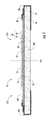
- FIG. 1 shows a cross-sectional view of a film resistor according to an embodiment of the present invention.
- FIG. 2 shows an enlarged cross-sectional view of a portion of the film resistor according to an embodiment of the present invention shown in FIG. 1 .
- FIG. 3 shows an enlarged cross-sectional view of a portion of a resistor according to an embodiment of the invention designated as “ FIG. 3 ” in FIG. 2 .
- FIG. 4 shows an enlarged cross-sectional view of a portion of a resistor according to an embodiment of the invention showing the area designated as “ FIG. 4 ” in FIG. 2 .
- FIG. 5 shows an enlarged cross-sectional view of a portion of a resistor according to an embodiment of the invention showing the area designated as “ FIG. 5 ” in FIG. 2 .
- FIG. 6 shows an enlarged cross-sectional view of a portion of a resistor according to an embodiment of the invention showing the area designated as “ FIG. 6 ” in FIG. 2 .
- FIG. 7 shows a top plan view of an exemplary mechanical mask for use in applying an alloy bond layer and thermally sprayed layer to a resistor according to the present invention.
- FIG. 7A shows a cross-sectional view of the width of an opening in the mechanical mask shown in FIG. 7 , taken along line A-A in FIG. 7 .
- FIG. 7B shows a cross-sectional view of the length of an opening in the mechanical mask shown in FIG. 7 , taken along line B-B in FIG. 7 .
- FIG. 8A shows a top surface of a resistor made according to the teachings of the present invention.
- FIG. 8B shows a bottom surface of a resistor made according to the terms of the present invention.
- FIG. 9 is a flow diagram illustrating a part of a manufacturing process of an embodiment of a thin film resistor of the present invention.
- FIG. 10 is a flow diagram illustrating a part of a manufacturing process of an embodiment of a thin film resistor of the present invention.
- FIG. 11 is a flow diagram illustrating a part of a manufacturing process of an embodiment of a thin film resistor of the present invention.
- FIG. 12 is a flow diagram illustrating a part of a manufacturing process of an embodiment of a thin film resistor of the present invention.
- FIG. 13 is a cross-sectional view of a portion of an embodiment of a resistor according to the present invention, showing a thermally sprayed resistive layer thermally sprayed directly to a substrate.
- FIG. 14 is a cross-sectional view of a portion of an embodiment of a resistor according to the present invention, showing the alloy bond layer extending along a portion of the upper surface of the substrate.
- FIG. 15 is a cross-sectional view of a portion of an embodiment of a resistor according to the present invention, showing a thick film conductor.
- FIG. 16 is an image of a cross-section of a portion of an exemplary resistor made according to the teachings of the present invention, using bright field illumination at 5 ⁇ magnification.
- FIG. 17 is an image of a cross-section of a portion of the exemplary resistor of FIG. 16 , using bright field illumination at 10 ⁇ magnification.
- FIG. 18 is an image of a cross-section of a portion of the exemplary resistor of FIG. 16 , using bright field illumination at 25 ⁇ magnification.
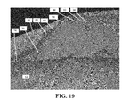
- FIG. 19 is an image of a cross-section of a portion of the exemplary resistor of FIG. 16 , using bright field illumination at 25 ⁇ magnification.
- FIG. 20 is a cross-sectional view of a portion of an embodiment of a resistor according to the present invention, showing a thermally sprayed conductor layer.
- the present invention is directed to the use and application of thermal spraying processes, techniques and technologies to the manufacture of thin film resistors.
- Table 1 provides a summary of typical thermal spraying processes, energy sources, environmental conditions, and the types of feedstock that may be used. Any of these methods could be used to achieve the rapid material deposition rates required for low resistance value thin film resistor manufacturing, as well as any others understood in the art to fall within the scope of thermal spraying.
- FIGS. 1-6 A thin film resistor according to an embodiment of the present invention is shown in FIGS. 1-6 .
- the thin film resistor as shown in the orientation of FIGS. 1-6 , has a top or upper side 202 (or first side), opposite side ends 204 (left), 206 (right) (also referred to as “side faces”), and a bottom or lower side 208 (or second side).
- the right portion 210 of the resistor 10 shown to the right of center line 214 is essentially a mirror image of the left portion 212 of the resistor shown to the left of center line 214 , as shown in the Figures. Thus, descriptions of the right portion 210 will also apply to the left portion 212 , unless otherwise indicated.
- a thin film resistor generally comprises a ceramic or non-metallic substrate 12 , an alloy bond layer 14 deposited on the substrate 12 , and a thermally sprayed resistive layer 18 thermally sprayed to the alloy bond layer 14 .
- the material to be used in forming the thermally sprayed resistive layer 18 may be referred to herein as the “thermally sprayed material 16 .”
- the thermally sprayed material 16 will be used as the feedstock for a thermal spraying process, to apply, by thermal spraying, the thermally sprayed resistive element 20 of a finished resistor.
- a potential difficulty with applying a thermally sprayed material to a ceramic or other non-metallic substrate lies in achieving a substantial bond strength, e.g., a bond that will not readily separate, between the thermally sprayed material and the underlying substrate or surface.
- a bond is achieved which is primarily mechanical.
- the surface of the substrate is grit blasted to remove oxides and to texture the surface thereby promoting mechanical adhesion between the feedstock and the substrate.
- the thickness of the ceramic substrate ranges generally between about 0.010 inches to 0.025 inches thick.
- Grit blasting of ceramic or non-metallic substrates of such a thickness can result in distortion of the substrate well before a sufficient surface roughness is achieved.
- known grit blasting techniques are inappropriate, and generally inapplicable, to the process of making a thin film resistor.
- an alloy bond layer 14 is deposited on the substrate 12 .
- the alloy bond layer 14 may comprise, for example, a nickel chromium alloy. Other alloys may be used depending on the alloy used for the thermally spray material that will be applied.
- the alloy bond layer 14 may comprise, but is not limited to, alloys comprising nickel, tantalum, titanium, copper and aluminum, other known alloys suitable for use as the alloy bond layer, or combinations thereof.
- the alloy bond layer 14 is preferably applied by a PVD process, but it is appreciated that other thin film deposition technologies and/or processes may be used. By use of the alloy bond layer 14 , grit blasting the substrate can therefore be avoided.
- FIGS. 1-3 show cross-sections of an exemplary resistor 10 fabricated according to an embodiment the present invention.
- an aluminum oxide or aluminum nitride ceramic substrate 12 is provided.
- any acceptable ceramic or other electrically non-conductive material for use in a thin film resistor may be used as the substrate 12 .
- metallic substrates that have an electrically non-conductive surface treatment may also be used.
- the alloy bond layer 14 is deposited, such as by a PVD process, on the substrate 12 .
- the alloy bond layer 14 preferably has a chemical composition similar to or complementary to the thermally sprayed resistive layer 18 that is to be applied.
- a copper, nickel, titanium or tantalum alloy is to be used to form the thermally sprayed resistive layer 18
- a corresponding copper, nickel, titanium or tantalum alloy would be used for the alloy bond layer 14 .
- the alloy bond layer 14 and the thermally sprayed material essentially correspond and have the same or a similar chemical composition.
- the thermally sprayed material 16 may preferably be a nickel chromium alloy having the same or a similar chemical composition. In this manner, a chemical bond may be formed between the thermally sprayed material 16 and the material of the alloy bond layer 14 .
- the alloy bond layer 14 is preferably formed using a PVD process, though other vapor deposition processes including, but not limited to, PECVD or CVD may be used.
- the alloy bond layer 14 forms a strong mechanical bond with the ceramic or nonmetallic surface of the substrate 12 .
- a thermally sprayed material 16 is thermally sprayed onto the alloy bond layer 14 to form a thermally sprayed resistive layer 18 .
- the thermally sprayed resistive layer 18 forms a thermally sprayed resistive element 20 , the size and shape of which can be adjusted during the manufacturing process.
- a thermal spraying process such as any described above or others known in the art, a chemical bond is formed between the thermally sprayed material 16 and the alloy bond layer 14 due to the similarities in their chemical composition.
- the thermally sprayed resistive element can be sprayed, for example, to a thickness of at least 3.94 mils (100 micrometers).
- a resistor may be formed on a substrate 12 according the principles of the present invention by using a thermal spraying process alone, without use of the alloy bond layer 14 , as an alternate embodiment.
- a thermal spraying process alone, without use of the alloy bond layer 14
- an alternate embodiment of a resistor may be formed according to the present invention with a thermally sprayed material 16 thermally sprayed directly to a substrate 12 of the resistor, without the use of an alloy bond layer 14 .
- mechanical masking may be used. This mechanical masking, shown in FIGS. 7A and 7B , defines the net resistor area A which in turn defines the resistance value of the subject resistors.
- a mechanical mask 22 is placed over the substrate.
- the size of the mechanical mask opening 24 can be selected to achieve a resistor area A having a particular resistance value. Accordingly, a method for selecting a specific resistance value is provided as part of the thermal spraying process described herein. This method is shown schematically in FIG. 12 , with the steps leading up to the thermally sprayed process to follow.
- a thin film resistor according to the present invention may have a low resistance value such as a resistance value of about 10.0 ohms or less, or a resistance value of about 1.0 ohms or less.
- thermally sprayed resistive element 20 can be selected to achieve a particular selected geometry having particular selected electrical properties.
- geometries that may be used for the thermally sprayed resistive element 20 include a block pattern, a serpentine pattern, a top hat pattern, and a ladder pattern. Accordingly, a method for selecting a resistive material geometry to achieve specific electrical properties is provided as part of the thermal spraying process and method of forming a thin film resistor as described herein.
- conductor pads 38 which may be single or multiple layers, as shown in FIGS. 1, 2 and 4 , may be formed to create a connection to the thermally sprayed resistive element 20 and thereby permit testing the properties of the thermally sprayed resistive element 20 .
- a vapor deposited adhesion layer 28 of an alloy for example, an adhesion layer 28 of a titanium alloy applied by, for example, a PVD process, is applied to a previously applied thermally sprayed resistive layer 18 .
- a first conductor layer 32 for example a first conductor layer 32 comprising gold, is preferably vapor deposited such as by PVD on the previously applied adhesion layer 28 .
- a photoresist may then be applied to the previously applied layers and patterned to further define an additional layer, if desired, of the conductor pads 38 .
- plating may be used to form a second conductor layer 36 , comprising, for example, gold, and the photoresist is removed.
- the second conductor layer 36 may be formed by thermal spraying.
- the conductor pads 38 which may be one or multiple layers, and the adhesion layer 28 may be etched, forming separate block resistors comprising the previously described thermally sprayed resistive layer 18 comprising, for example, nickel chromium alloy, with conductor pads 38 , which may comprise gold, at the end of each block.
- thermally sprayed resistive layer 18 formed from thermally sprayed material 16 comprising, for example, copper, nickel, titanium or tantalum, or alloys thereof.
- the thermally sprayed resistive layer 18 forms a thermally sprayed resistive element 20 of a finished resistor.
- the thermally sprayed resistive element 20 is thus made up of feedstock particles, “drops,” “splats” or “lamellae” of the thermally sprayed material 16 , formed by the liquefied droplets or plastically deformed particles of the thermally sprayed material 16 selected.
- the thermally sprayed resistive element 20 will demonstrate the properties of a thermally sprayed coating using the thermal spraying techniques described herein, or related thermal spraying techniques.
- the thermally sprayed resistive element 20 will comprise particles demonstrating mechanical interlocking or bonding, diffusion bonding, metallurgical bonding, or other adhesive, chemical or physical bonding properties, or combinations of these, depending on the nature and composition of the particles of the thermally sprayed material 16 .
- a thermally sprayed resistive element can be deposited at a rate of between about 10 to 60 micrometers per minute, to form a thin film resistor as described herein.
- conductor pads 38 may be accomplished using a vapor deposited adhesion layer and seed layers (e.g., the PVD deposited layers that are used to initiate the electrolytic plating process, such a PVD deposited gold layer thick enough to initiate the electrolytic gold plating process), followed by, for example, a plating process, other processes and materials may be used to form the conductor pads 38 .
- a vapor deposited adhesion layer and seed layers e.g., the PVD deposited layers that are used to initiate the electrolytic plating process, such a PVD deposited gold layer thick enough to initiate the electrolytic gold plating process
- other processes and materials may be used to form the conductor pads 38 .
- an additional mechanical mask and an additional thermal spraying process may be used to form the conductor pads 38 .
- a typical thick film technology process as known in the art may be used to apply thick film conductor pads 34 to the surface of the substrate 12 prior to depositing the resistive materials.
- Thick film materials and processes are used to make thick film chip resistors, resistor networks, hybrid substrates, and other electronic components and circuits.
- a thick film conductor material could be screen printed onto a bare ceramic substrate as a thick film conductor layer 34 , and subjected to a firing process to melt the inorganic binders in the thick film paste, thereby bonding the thick film conductor layer 34 to the substrate 12 .
- Thick film conductors may contain silver or silver alloys, copper, or gold as the conductive phase, and an inorganic binder such as glass to bond the conductive phase to the substrate.
- an alloy bond layer 14 may be applied, using a range of known methods, overlapping onto the thick film conductor pad 34 . With the alloy bond layer 14 in place, the thermally sprayed resistive layer 18 would be applied using a mechanical mask such as described.
- Termination patterns or designs can be varied to modify the resistor geometry in order to increase or decrease the square count of the resistor and to impact or otherwise control the electrical properties of the finished resistor.
- the geometry of the thermally sprayed resistive element 20 may be modified using laser trimming and/or machining processes to achieve the desired resistance value. While laser trimming may be used, other processes may be used including, but not limited to, chemical etching, grinding or abrasive machining, to establish the final resistance value.
- an overcoat 50 may be applied to the thermally sprayed resistive layer 18 comprising a moisture passivation layer 40 and a mechanical protection layer 42 .
- the moisture passivation layer 40 may be, for example, a polymer
- the mechanical protection layer 42 may be, for example, an epoxy.
- an electrical connection from the upper side 202 of the device to the bottom side 208 of the devices is made by one or more additional layers. As shown for example in FIGS. 2 and 5-6 , this may be accomplished using a PVD process to apply a nickel alloy adhesion layer 54 followed by a nickel alloy conductor layer 56 (which may also be considered and/or referred to as a third conductor layer) overlapping the conductor pads 38 and extending around the end of the device onto the bottom of the substrate 12 .
- a PVD process to apply a nickel alloy adhesion layer 54 followed by a nickel alloy conductor layer 56 (which may also be considered and/or referred to as a third conductor layer) overlapping the conductor pads 38 and extending around the end of the device onto the bottom of the substrate 12 .
- a fourth conductor layer 52 may be plated to the desired thickness followed by a nickel barrier layer 48 .
- the final plating step may be the application of a tin/lead or lead free solder 46 finish. While PVD deposited nickel alloys were used for the adhesion layer 54 , followed by a plated copper conductor layer 52 , alternative processes and materials may be used to form the connection from the upper side 202 to the bottom side 208 of the device.
- the alloy bond layer 14 extends along a majority of the upper surface of the substrate 12 .
- the thermally sprayed resistive element 20 extends along a majority of the alloy bond layer 14 .
- the adhesion layer 28 and conductor pads 38 are positioned on opposite side ends of the thermally sprayed resistive element 20 , and at least partially overlap an upper surface of the thermally sprayed resistive element 20 at the opposite side ends.
- the adhesion layer 28 and conductor pads 38 may extend toward the side ends 204 , 206 of the resistor 10 and to adjacent the end of the alloy bond layer 14 .
- the parts of the thermally sprayed resistive element 20 that remains exposed after the adhesion layer 28 and conductor pads 38 are applied may be covered by the moisture passivation layer 40 , which can extend along a length of an upper surface of the thermally sprayed resistive element 20 to adjacent the adhesion layers 28 and conductor pads 38 , and may at least partially cover an upper surface the conductor pads 38 .
- the mechanical protection layer 42 covers an upper surface of the moisture passivation layer 40 , and may completely cover the moisture passivation layer 40 .
- the mechanical protection layer 42 may also extend to cover edges of the upper surface of the conductor pads 38 .
- the adhesion layer 54 , third conductor layer 56 , fourth conductor layer 52 , barrier layer 48 and solder layer 46 may have a first end adjacent to and abutting the moisture passivation layer 40 and mechanical protection layer 42 , extending around the side ends 204 , 206 , and extending along at least a portion of the bottom 208 of the resistor, as shown for example in FIGS. 1 and 2 .
- the alloy bond layer 14 can alternately extend a shorter distance (shown extending to line D 1 in FIG. 14 ) along the upper surface of the substrate and extending directly beneath the thermally sprayed resistive layer 18 , but not extending beneath the adhesion layer 28 .
- the adhesion layer 28 is applied directly to the substrate 12 on opposite sides of the alloy bond layer 14 and thermally sprayed resistive layer 18 , and the additional layers may be applied and positioned as described in connection with FIGS. 1-6 , and as shown in FIG. 14 .
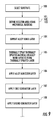
- FIGS. 9-11 An exemplary method of manufacturing a thin film resistor according to the teachings of the present invention is shown diagrammatically in FIGS. 9-11 .
- a substrate 12 is selected.
- the substrate 12 may be, for example, an aluminum oxide or aluminum nitride substrate.
- a mechanical mask is positioned to define the resistor area A and therefore the resistive value V of the resistor.
- the size of the resistor area A and selection of the size of the mechanical mask openings 24 to provide a particular resistor value V can be provided according to steps 101 - 103 of FIG. 12 .
- the alloy bond layer 14 is deposited.
- the alloy bond layer 14 may be a thin film nickel alloy applied by a PVD process.
- a thermal spraying process is used to spray the thermally sprayed material 16 on the alloy bond layer 14 , to form a thermally sprayed resistive layer 18 .
- the thermally sprayed material 16 may be a copper alloy, nickel alloy, titanium alloy or tantalum alloy.
- a nickel alloy bond layer 14 is used, and is then thermally sprayed with a nickel alloy thermally sprayed material 16 .
- an alloy adhesion layer 28 is deposited on a top or first surface of the thermally sprayed resistive layer 18 adjacent the opposite side ends of the thermally sprayed resistive layer 18 .
- the alloy adhesion layer 28 is also applied to at least a portion of a top or first surface of the alloy bond layer 14 on opposite sides of the thermally sprayed resistive layer 18 , as shown in FIGS. 1 and 2 .
- the alloy adhesion layer 28 may be a PVD applied thin film titanium alloy.
- a first conductor layer 32 is applied over the alloy adhesion layer 28 .
- the first conductor layer 32 may be a PVD applied thin film gold or copper conductor layer.
- a second conductor layer 36 is applied over the first conductor layer 32 .
- the second conductor layer 36 may be gold or copper, and may be applied by thermal spraying or plating techniques.
- the overcoat 50 is applied along a length of the upper surface of the thermally sprayed resistive layer 18 and covering the majority of the thermally sprayed resistive layer 18 , and portions of the conductor pads 38 , as shown in FIGS. 1 and 4 .
- the moisture passivation 40 is applied.
- the moisture passivation layer 40 may be applied by screen printing.
- the moisture passivation layer 40 covers a length, which may be a majority of the length, of the upper surface of the thermally sprayed resistive layer 18 , and may extend adjacent to and may overlap edge portions of the conductor pads 38 , as shown in FIG. 4 .
- the mechanical protection layer 42 is applied, such as by screen printing.
- the mechanical protection layer 42 covers a central portion of the moisture passivation layer 40 , and may also cover portions of the top surface of the conductor pads 38 adjacent to the moisture passivation layer 40 , as shown in FIGS. 1, 2 and 4 .
- the overcoat 50 assists in sealing and protecting portions of the upper surface of the resistor.
- a nickel alloy adhesion layer 54 is applied to the substrate, extending along a top surface of the substrate 12 adjacent the side ends of the alloy bond layer 14 , along opposite side surfaces of the substrate, and along portions of the bottom surface of the substrate 12 , as shown in FIGS. 1, 2, 5 and 6 .
- the alloy adhesion layer 54 may be a nickel alloy, and applied by a PVD process.
- a third conductor layer 56 is applied over the alloy adhesion layer 54 and extending from adjacent opposite ends of the mechanical protection layer and overlapping opposite top surfaces of the conductor pads 38 , along opposite side surfaces of the substrate, and along portions of the bottom surface of the substrate 12 , as shown in FIGS. 1, 2, 5 and 6 .
- the third conductor layer 56 may be a PVD applied thin film nickel alloy conductor layer.
- a fourth conductor layer 52 is applied overlapping the third conductor layer 56 , as shown in FIGS. 1, 2, 5 and 6 .
- the fourth conductor layer 52 may be plated nickel or copper.
- a nickel barrier layer is applied, such as by plating.
- a finishing solder layer 46 is applied, which may be “hot dipped” or plated tin or tin/lead alloy.
- FIGS. 9-12 can take place in an order accommodating the fabrication and manufacturing needs and equipment of a thin film resistor manufacturer.
- FIGS. 9-12 show steps of manufacturing a thin film resistor according to the present invention in an illustrative order, however, there may be variations in the order.
- manufacturing variables e.g., type of equipment used, pressure, temperature, environment
- a thermally sprayed resistive layer 18 may be applied directly to the surface of a substrate 12 , to form thermally sprayed resistive element, without the use of an alloy bond layer 14 .
- the resistor may be further fabricated using additional layers and processes as described herein.
- the conductor pads 38 may be formed by applying a thermally sprayed alloy directly to the thermally sprayed resistive layer 18 to form the conductor pads 38 , without applying an adhesion layer 28 .
- a thermally sprayed alloy may be applied directly to the surface of the substrate 12 to form a thermally sprayed conductor layer 58 , prior to applying the alloy bond layer 14 , with the thermally sprayed conductor layer 58 acting as the conductor pads.
- the alloy bond layer 14 may then be applied directly to the surface of the substrate 12 , overlapping onto the thermally sprayed conductor layer 58 .
- the thermally sprayed alloy is then applied to the surface of the alloy bond layer 14 including an area of overlap on the thermally sprayed conductor layer 58 .
- Various additional layers as described herein may be also applied.
- a PVD applied copper alloy conductor layer may be applied directly to the surface of the conductor pad 38 , extending onto the surface of the substrate 12 , around the side ends 204 , 206 of the resistor and onto the bottom of the substrate 12 , thereby replacing the nickel alloy adhesion layer 28 and the nickel alloy conductor layer 32 .
- a PVD copper alloy may also be applied in combination with an alloy adhesion layer, such as a nickel alloy, directly to the surface of the conductor pads 38 , extending onto the surface of the substrate 12 , around the side ends 204 , 206 of the resistor and onto the bottom of the substrate 12 , thereby replacing or as an alternative to the nickel alloy adhesion layer 54 and the nickel alloy conductor layer 56 shown in FIG. 5 .
- an alloy adhesion layer such as a nickel alloy
- FIG. 8A shows a top view of a resistor 10 made according to an embodiment of the present invention using thermal spraying techniques
- FIG. 8B shows a bottom view of the resistor 10
- a finished thin film resistor according to the invention has an appearance similar to typical thin film chip resistors made without the benefit of the thermal spraying techniques described herein, but can be produced at a much lower cost and at resistance values well below those of typical thin film product.
- FIGS. 16-19 show enlarged images of cross sections of an exemplary thin film resistor according to the teachings of the present invention at various magnifications.
- a thin film resistor 10 was formed with an aluminum oxide substrate 12 .
- a PVD applied thin film nickel alloy bond layer 14 was applied to a portion of the top surface of the substrate 12 .
- a nickel chromium alloy was thermally sprayed over a portion of the alloy bond layer 14 to form a thermally sprayed resistive element 20 .
- a moisture passivation layer 40 was screen printed on a portion of the upper surface of the thermally sprayed resistive layer 18 , and a mechanical protection layer 42 was screen printed over a portion of the moisture passivation layer 40 to form an overcoat 50 .
- a PVD applied thin film titanium alloy adhesion layer 28 was applied at sides of the upper surface of the thermally sprayed resistive layer 18 .
- a PVD applied thin film gold first conductor layer 32 was applied over the alloy adhesion layer 28 .
- a gold second conductor layer 36 was plated over the first conductor layer 32 .
- a nickel barrier layer 48 was applied by plating running from the conductor pads 38 along the sides of the substrate 12 , and along a portion of the bottom of the substrate.
- a thin film nickel alloy conductor layer 56 was applied by PVD over the adhesion layer.
- a copper conductor layer 52 was applied by plating over the nickel alloy conductor layer 56 .
- a nickel barrier layer 48 was applied by plating over the copper conductor layer 52 .
- a hot dipped lead free solder layer 46 was applied over the nickel barrier layer 48 .
- thermally sprayed material 16 a nickel chromium alloy was used as the thermally sprayed material 16 .
- low resistance value thin film resistors can also be made according to the present invention using other metal alloys such as MANGANIN® and EVANOHM®, or metal alloys including but not limited to those comprising copper, tantalum and titanium.
- the thermally sprayed material 16 may be a combination of alloys selected to achieve particular electrical properties, such as a particular temperature coefficient or resistance (TCR) profile (e.g., a net flat TCR profile) or resistivity.
- TCR temperature coefficient or resistance
Abstract
Description
| TABLE 1 | |||
| Type of | |||
| Thermal | Type of Energy | Spray Process | Type of |
| Spray Process | Source | Environment | Feedstock |
| Atmospheric | High Temperature | Ambient | Powder |
| Plasma Spray | Plasma | ||
| High Velocity | High | Ambient | Powder |
| Oxygen | Temperature | ||
| Fuel (HVOF) | Combustion | ||
| Electric Wire Arc | Thermal Energy | Ambient | Wire |
| From Wire Arc | |||
| Cold Spray | Kinetic Energy | Ambient or | Powder |
| Controlled | |||
| Atmosphere | |||
| Combustion Wire | Thermal Energy | Ambient | Wire |
| Spray (Flame | From | ||
| Spray) | Combustion Process | ||
| Combustion | Thermal Energy | Ambient | Powder |
| Powder | From | ||
| Spray (Flame | Combustion Process | ||
| Spray) | |||
| Controlled | High Temperature | Controlled | Powder |
| Atmosphere | Plasma | Atmosphere | |
| Plasma Spray | |||
Claims (30)
Priority Applications (9)
| Application Number | Priority Date | Filing Date | Title |
|---|---|---|---|
| US14/563,560 US9818512B2 (en) | 2014-12-08 | 2014-12-08 | Thermally sprayed thin film resistor and method of making |
| KR1020177018773A KR20170092676A (en) | 2014-12-08 | 2015-12-04 | Thermally sprayed thin film resistor and method of making |
| EP15868328.4A EP3230486A4 (en) | 2014-12-08 | 2015-12-04 | Thermally sprayed thin film resistor and method of making |
| CN201580073487.9A CN107109613A (en) | 2014-12-08 | 2015-12-04 | thermal spraying film resistor and preparation method thereof |
| PCT/US2015/063887 WO2016094211A1 (en) | 2014-12-08 | 2015-12-04 | Thermally sprayed thin film resistor and method of making |
| JP2017530060A JP2018502988A (en) | 2014-12-08 | 2015-12-04 | Thermal spray type thin film resistor and manufacturing method |
| TW104141087A TW201637030A (en) | 2014-12-08 | 2015-12-08 | Thermally sprayed thin film resistor and method of making |
| IL252673A IL252673A0 (en) | 2014-12-08 | 2017-06-05 | Thermally sprayed thin film resistor and method of making |
| HK18102631.1A HK1243146A1 (en) | 2014-12-08 | 2018-02-23 | Thermally sprayed thin film resistor and method of making |
Applications Claiming Priority (1)
| Application Number | Priority Date | Filing Date | Title |
|---|---|---|---|
| US14/563,560 US9818512B2 (en) | 2014-12-08 | 2014-12-08 | Thermally sprayed thin film resistor and method of making |
Publications (2)
| Publication Number | Publication Date |
|---|---|
| US20160163432A1 US20160163432A1 (en) | 2016-06-09 |
| US9818512B2 true US9818512B2 (en) | 2017-11-14 |
Family
ID=56094909
Family Applications (1)
| Application Number | Title | Priority Date | Filing Date |
|---|---|---|---|
| US14/563,560 Expired - Fee Related US9818512B2 (en) | 2014-12-08 | 2014-12-08 | Thermally sprayed thin film resistor and method of making |
Country Status (9)
| Country | Link |
|---|---|
| US (1) | US9818512B2 (en) |
| EP (1) | EP3230486A4 (en) |
| JP (1) | JP2018502988A (en) |
| KR (1) | KR20170092676A (en) |
| CN (1) | CN107109613A (en) |
| HK (1) | HK1243146A1 (en) |
| IL (1) | IL252673A0 (en) |
| TW (1) | TW201637030A (en) |
| WO (1) | WO2016094211A1 (en) |
Cited By (1)
| Publication number | Priority date | Publication date | Assignee | Title |
|---|---|---|---|---|
| US10982310B2 (en) | 2018-04-09 | 2021-04-20 | ResOps, LLC | Corrosion resistant thermal spray alloy |
Families Citing this family (8)
| Publication number | Priority date | Publication date | Assignee | Title |
|---|---|---|---|---|
| US9818512B2 (en) * | 2014-12-08 | 2017-11-14 | Vishay Dale Electronics, Llc | Thermally sprayed thin film resistor and method of making |
| WO2019102857A1 (en) * | 2017-11-27 | 2019-05-31 | パナソニックIpマネジメント株式会社 | Resistor |
| JP7217419B2 (en) * | 2017-11-27 | 2023-02-03 | パナソニックIpマネジメント株式会社 | Resistor |
| DE102018204428A1 (en) * | 2018-03-22 | 2019-09-26 | Enrico Flade | Flat heating element |
| JP2020010004A (en) * | 2018-07-12 | 2020-01-16 | Koa株式会社 | Resistor and circuit substrate |
| TWI708856B (en) * | 2019-06-18 | 2020-11-01 | 國立中山大學 | Method for manufacturing a thin film resistor |
| KR102231103B1 (en) * | 2019-12-10 | 2021-03-23 | 삼성전기주식회사 | Resistor element |
| WO2024017494A1 (en) * | 2022-07-19 | 2024-01-25 | Oerlikon Metco Ag, Wohlen | Electric heating element production method |
Citations (46)
| Publication number | Priority date | Publication date | Assignee | Title |
|---|---|---|---|---|
| US4152689A (en) | 1978-02-13 | 1979-05-01 | American Components Inc. | Electrical resistor package which remains unaffected by ambient stresses and humidity |
| US4677413A (en) | 1984-11-20 | 1987-06-30 | Vishay Intertechnology, Inc. | Precision power resistor with very low temperature coefficient of resistance |
| US4808490A (en) | 1983-12-28 | 1989-02-28 | Hitachi Metals, Ltd. | Plasma sprayed film resistor heater |
| JPH08203713A (en) | 1995-01-20 | 1996-08-09 | Matsushita Electric Ind Co Ltd | Manufacture of square with film chip resistor |
| US5966067A (en) | 1997-12-26 | 1999-10-12 | E. I. Du Pont De Nemours And Company | Thick film resistor and the manufacturing method thereof |
| US6136512A (en) | 1997-10-29 | 2000-10-24 | International Business Machines Corporation | Method of forming resistors |
| US6153256A (en) | 1998-08-18 | 2000-11-28 | Rohm Co., Ltd. | Chip resistor and method of making the same |
| JP2001023801A (en) | 1999-07-05 | 2001-01-26 | Rohm Co Ltd | Construction of chip resistor |
| US6201290B1 (en) | 1998-01-08 | 2001-03-13 | Matsushita Electric Industrial Co., Ltd. | Resistor having moisture resistant layer |
| JP2001110601A (en) | 1999-10-14 | 2001-04-20 | Matsushita Electric Ind Co Ltd | Resistor and manufacturing method therefor |
| JP2001143905A (en) | 1999-11-17 | 2001-05-25 | Murata Mfg Co Ltd | Method of manufacturing chip type thermistor |
| US6242999B1 (en) | 1998-01-20 | 2001-06-05 | Matsushita Electric Industrial Co., Ltd. | Resistor |
| US20020031860A1 (en) | 2000-04-20 | 2002-03-14 | Rohm Co., Ltd. | Chip resistor and method for manufacturing the same |
| JP2002184602A (en) | 2000-12-13 | 2002-06-28 | Matsushita Electric Ind Co Ltd | Angular chip resistor unit |
| US6428630B1 (en) | 2000-05-18 | 2002-08-06 | Sermatech International, Inc. | Method for coating and protecting a substrate |
| JP2002299203A (en) | 2001-03-29 | 2002-10-11 | Mitsubishi Electric Corp | Method for fabricating semiconductor device |
| US20020148106A1 (en) | 2001-04-16 | 2002-10-17 | Torayuki Tsukada | Chip resistor fabrication method |
| JP2002305126A (en) | 2001-04-06 | 2002-10-18 | Koa Corp | Chip resistor |
| EP1271566A2 (en) | 2001-06-20 | 2003-01-02 | Alps Electric Co., Ltd. | Thin-film resistor and method for manufacturing the same |
| JP2003124004A (en) | 2001-10-11 | 2003-04-25 | Koa Corp | Chip resistor and method of fabrication |
| US20030117258A1 (en) | 2001-12-20 | 2003-06-26 | Samsung Electro-Mechanics Co., Ltd. | Thin film chip resistor and method for fabricating the same |
| JP2003203801A (en) | 2002-01-08 | 2003-07-18 | Koa Corp | Chip resistor and its manufacturing method |
| JP2003282305A (en) | 2002-03-25 | 2003-10-03 | Koa Corp | Chip resistor and its manufacturing method |
| JP2003282302A (en) | 2002-03-25 | 2003-10-03 | Koa Corp | Chip resistor |
| JP2003282304A (en) | 2002-03-25 | 2003-10-03 | Koa Corp | Chip resistor and its manufacturing method |
| US6762396B2 (en) * | 1997-05-06 | 2004-07-13 | Thermoceramix, Llc | Deposited resistive coatings |
| US20040262712A1 (en) | 2001-11-28 | 2004-12-30 | Masato Doi | Chip resistor and method for making the same |
| US6943662B2 (en) | 2001-11-30 | 2005-09-13 | Rohm Co., Ltd. | Chip resistor |
| JP2005258302A (en) | 2004-03-15 | 2005-09-22 | Yamaha Corp | Device and method to drive playing operator of automatic playing musical instrument |
| JP2006024767A (en) | 2004-07-08 | 2006-01-26 | Koa Corp | Manufacturing method of chip resistor |
| US7057490B2 (en) | 2000-08-30 | 2006-06-06 | Matsushita Electric Industrial Co. Ltd. | Resistor and production method therefor |
| JP2006186064A (en) | 2004-12-27 | 2006-07-13 | Koa Corp | Chip resistor |
| JP2007095926A (en) | 2005-09-28 | 2007-04-12 | Koa Corp | Chip resistor |
| US20080094169A1 (en) | 2004-09-15 | 2008-04-24 | Yasuharu Kinoshita | Chip-Shaped Electronic Part |
| US20090308454A1 (en) | 2008-06-12 | 2009-12-17 | General Electric Company, A New York Corporation | Insulating coating, methods of manufacture thereof and articles comprising the same |
| US7782173B2 (en) | 2005-09-21 | 2010-08-24 | Koa Corporation | Chip resistor |
| US7839000B2 (en) | 2002-06-25 | 2010-11-23 | Unitive International Limited | Solder structures including barrier layers with nickel and/or copper |
| US20110100975A1 (en) | 2009-11-03 | 2011-05-05 | Industrial Technology Research Institute | Carrier for heating and keeping warm |
| JP2011091140A (en) | 2009-10-21 | 2011-05-06 | Koa Corp | Chip resistor to be built in substrate and method of manufacturing the same |
| US7982582B2 (en) | 2007-03-01 | 2011-07-19 | Vishay Intertechnology Inc. | Sulfuration resistant chip resistor and method for making same |
| US20110188838A1 (en) * | 2008-05-30 | 2011-08-04 | Thermoceramix, Inc. | Radiant heating using heater coatings |
| JP2011238730A (en) | 2010-05-10 | 2011-11-24 | Koa Corp | Chip resistor and its mounting structure |
| US20140308883A1 (en) * | 2013-04-08 | 2014-10-16 | Chien-Min Sung | Chemical mechanical polishing conditioner |
| US20160035466A1 (en) * | 2014-07-31 | 2016-02-04 | Thinking Electronic Industrial Co., Ltd. | Electrode component with pretreated layers |
| US20160145159A1 (en) * | 2014-11-24 | 2016-05-26 | Rolls-Royce Corporation | Bond layer for silicon-containing substrates |
| US20160163432A1 (en) * | 2014-12-08 | 2016-06-09 | Vishay Dale Electronics, Inc. | Thermally sprayed thin film resistor and method of making |
Family Cites Families (4)
| Publication number | Priority date | Publication date | Assignee | Title |
|---|---|---|---|---|
| CN101638765A (en) * | 2000-11-29 | 2010-02-03 | 萨莫希雷梅克斯公司 | Resistive heaters and uses thereof |
| US8680443B2 (en) * | 2004-01-06 | 2014-03-25 | Watlow Electric Manufacturing Company | Combined material layering technologies for electric heaters |
| US8242878B2 (en) * | 2008-09-05 | 2012-08-14 | Vishay Dale Electronics, Inc. | Resistor and method for making same |
| DE102012202374A1 (en) * | 2012-02-16 | 2013-08-22 | Webasto Ag | Vehicle heating and method for producing a vehicle heater |
-
2014
- 2014-12-08 US US14/563,560 patent/US9818512B2/en not_active Expired - Fee Related
-
2015
- 2015-12-04 JP JP2017530060A patent/JP2018502988A/en active Pending
- 2015-12-04 EP EP15868328.4A patent/EP3230486A4/en not_active Withdrawn
- 2015-12-04 CN CN201580073487.9A patent/CN107109613A/en active Pending
- 2015-12-04 KR KR1020177018773A patent/KR20170092676A/en unknown
- 2015-12-04 WO PCT/US2015/063887 patent/WO2016094211A1/en active Application Filing
- 2015-12-08 TW TW104141087A patent/TW201637030A/en unknown
-
2017
- 2017-06-05 IL IL252673A patent/IL252673A0/en unknown
-
2018
- 2018-02-23 HK HK18102631.1A patent/HK1243146A1/en unknown
Patent Citations (50)
| Publication number | Priority date | Publication date | Assignee | Title |
|---|---|---|---|---|
| US4152689A (en) | 1978-02-13 | 1979-05-01 | American Components Inc. | Electrical resistor package which remains unaffected by ambient stresses and humidity |
| US4808490A (en) | 1983-12-28 | 1989-02-28 | Hitachi Metals, Ltd. | Plasma sprayed film resistor heater |
| US4677413A (en) | 1984-11-20 | 1987-06-30 | Vishay Intertechnology, Inc. | Precision power resistor with very low temperature coefficient of resistance |
| JPH08203713A (en) | 1995-01-20 | 1996-08-09 | Matsushita Electric Ind Co Ltd | Manufacture of square with film chip resistor |
| US6762396B2 (en) * | 1997-05-06 | 2004-07-13 | Thermoceramix, Llc | Deposited resistive coatings |
| US6136512A (en) | 1997-10-29 | 2000-10-24 | International Business Machines Corporation | Method of forming resistors |
| US5966067A (en) | 1997-12-26 | 1999-10-12 | E. I. Du Pont De Nemours And Company | Thick film resistor and the manufacturing method thereof |
| US6201290B1 (en) | 1998-01-08 | 2001-03-13 | Matsushita Electric Industrial Co., Ltd. | Resistor having moisture resistant layer |
| US6242999B1 (en) | 1998-01-20 | 2001-06-05 | Matsushita Electric Industrial Co., Ltd. | Resistor |
| US6153256A (en) | 1998-08-18 | 2000-11-28 | Rohm Co., Ltd. | Chip resistor and method of making the same |
| JP2001023801A (en) | 1999-07-05 | 2001-01-26 | Rohm Co Ltd | Construction of chip resistor |
| JP2001110601A (en) | 1999-10-14 | 2001-04-20 | Matsushita Electric Ind Co Ltd | Resistor and manufacturing method therefor |
| JP2001143905A (en) | 1999-11-17 | 2001-05-25 | Murata Mfg Co Ltd | Method of manufacturing chip type thermistor |
| US20020031860A1 (en) | 2000-04-20 | 2002-03-14 | Rohm Co., Ltd. | Chip resistor and method for manufacturing the same |
| US6428630B1 (en) | 2000-05-18 | 2002-08-06 | Sermatech International, Inc. | Method for coating and protecting a substrate |
| US7057490B2 (en) | 2000-08-30 | 2006-06-06 | Matsushita Electric Industrial Co. Ltd. | Resistor and production method therefor |
| JP2002184602A (en) | 2000-12-13 | 2002-06-28 | Matsushita Electric Ind Co Ltd | Angular chip resistor unit |
| JP2002299203A (en) | 2001-03-29 | 2002-10-11 | Mitsubishi Electric Corp | Method for fabricating semiconductor device |
| JP2002305126A (en) | 2001-04-06 | 2002-10-18 | Koa Corp | Chip resistor |
| US20020148106A1 (en) | 2001-04-16 | 2002-10-17 | Torayuki Tsukada | Chip resistor fabrication method |
| EP1271566A2 (en) | 2001-06-20 | 2003-01-02 | Alps Electric Co., Ltd. | Thin-film resistor and method for manufacturing the same |
| JP2003124004A (en) | 2001-10-11 | 2003-04-25 | Koa Corp | Chip resistor and method of fabrication |
| US7098768B2 (en) | 2001-11-28 | 2006-08-29 | Rohm Co., Ltd. | Chip resistor and method for making the same |
| US20040262712A1 (en) | 2001-11-28 | 2004-12-30 | Masato Doi | Chip resistor and method for making the same |
| US6943662B2 (en) | 2001-11-30 | 2005-09-13 | Rohm Co., Ltd. | Chip resistor |
| US20030117258A1 (en) | 2001-12-20 | 2003-06-26 | Samsung Electro-Mechanics Co., Ltd. | Thin film chip resistor and method for fabricating the same |
| JP2003203801A (en) | 2002-01-08 | 2003-07-18 | Koa Corp | Chip resistor and its manufacturing method |
| JP2003282302A (en) | 2002-03-25 | 2003-10-03 | Koa Corp | Chip resistor |
| JP2003282304A (en) | 2002-03-25 | 2003-10-03 | Koa Corp | Chip resistor and its manufacturing method |
| JP2003282305A (en) | 2002-03-25 | 2003-10-03 | Koa Corp | Chip resistor and its manufacturing method |
| US7839000B2 (en) | 2002-06-25 | 2010-11-23 | Unitive International Limited | Solder structures including barrier layers with nickel and/or copper |
| JP2005258302A (en) | 2004-03-15 | 2005-09-22 | Yamaha Corp | Device and method to drive playing operator of automatic playing musical instrument |
| JP2006024767A (en) | 2004-07-08 | 2006-01-26 | Koa Corp | Manufacturing method of chip resistor |
| US20080094169A1 (en) | 2004-09-15 | 2008-04-24 | Yasuharu Kinoshita | Chip-Shaped Electronic Part |
| JP2006186064A (en) | 2004-12-27 | 2006-07-13 | Koa Corp | Chip resistor |
| US7782173B2 (en) | 2005-09-21 | 2010-08-24 | Koa Corporation | Chip resistor |
| JP2007095926A (en) | 2005-09-28 | 2007-04-12 | Koa Corp | Chip resistor |
| US20120126934A1 (en) | 2007-03-01 | 2012-05-24 | Vishay Intertechnology, Inc. | Sulfuration resistant chip resistor and method for making same |
| US7982582B2 (en) | 2007-03-01 | 2011-07-19 | Vishay Intertechnology Inc. | Sulfuration resistant chip resistor and method for making same |
| US8514051B2 (en) | 2007-03-01 | 2013-08-20 | Vishay Intertechnology, Inc. | Sulfuration resistant chip resistor and method for making same |
| US8957756B2 (en) | 2007-03-01 | 2015-02-17 | Vishay Intertechnology, Inc. | Sulfuration resistant chip resistor and method for making same |
| US20110188838A1 (en) * | 2008-05-30 | 2011-08-04 | Thermoceramix, Inc. | Radiant heating using heater coatings |
| US20090308454A1 (en) | 2008-06-12 | 2009-12-17 | General Electric Company, A New York Corporation | Insulating coating, methods of manufacture thereof and articles comprising the same |
| JP2011091140A (en) | 2009-10-21 | 2011-05-06 | Koa Corp | Chip resistor to be built in substrate and method of manufacturing the same |
| US20110100975A1 (en) | 2009-11-03 | 2011-05-05 | Industrial Technology Research Institute | Carrier for heating and keeping warm |
| JP2011238730A (en) | 2010-05-10 | 2011-11-24 | Koa Corp | Chip resistor and its mounting structure |
| US20140308883A1 (en) * | 2013-04-08 | 2014-10-16 | Chien-Min Sung | Chemical mechanical polishing conditioner |
| US20160035466A1 (en) * | 2014-07-31 | 2016-02-04 | Thinking Electronic Industrial Co., Ltd. | Electrode component with pretreated layers |
| US20160145159A1 (en) * | 2014-11-24 | 2016-05-26 | Rolls-Royce Corporation | Bond layer for silicon-containing substrates |
| US20160163432A1 (en) * | 2014-12-08 | 2016-06-09 | Vishay Dale Electronics, Inc. | Thermally sprayed thin film resistor and method of making |
Non-Patent Citations (5)
| Title |
|---|
| Gabel, Howard, "Kinetic Metallization Compared with HVO," Advanced Materials and Processes/ May 2004 (pp. 17 and 48). |
| Inovati, "KM-Production Coating System," KM Data Sheet, Form PCS-10, copyright 2010 (1 page), downloaded from http://www.inovati.com/. The year of publication is sufficiently earlier than the effective U.S. filing date and any foreign priority date so that the particular month of publication is not in issue. |
| Leyman, "Supersonic Particle Deposition (Cold Spray)," US Army Research Laboratory, Weapons & Materials Research Doctorate, HCAT Program Review Meeting, Jul. 20-21, 2004 (24 pages). |
| Sulzer Metco, "An Introduction to Thermal Spray," Issue 4, copyright 2012 (24 pages). The year of publication is sufficiently earlier than the effective U.S. filing date and any foreign priority date so that the particular month of publication is not in issue. |
| Vishay Intertechnology, Inc., "Resistors 101," Instructional Guide, date code "VMN-SG2113-1205" referring to publication in 2012, pp. 1-8. The year of publication is sufficiently earlier than the effective U.S. filing date and any foreign priority date so that the particular month of publication is not in issue. |
Cited By (1)
| Publication number | Priority date | Publication date | Assignee | Title |
|---|---|---|---|---|
| US10982310B2 (en) | 2018-04-09 | 2021-04-20 | ResOps, LLC | Corrosion resistant thermal spray alloy |
Also Published As
| Publication number | Publication date |
|---|---|
| IL252673A0 (en) | 2017-08-31 |
| EP3230486A1 (en) | 2017-10-18 |
| CN107109613A (en) | 2017-08-29 |
| TW201637030A (en) | 2016-10-16 |
| HK1243146A1 (en) | 2018-07-06 |
| JP2018502988A (en) | 2018-02-01 |
| EP3230486A4 (en) | 2018-10-31 |
| WO2016094211A1 (en) | 2016-06-16 |
| US20160163432A1 (en) | 2016-06-09 |
| KR20170092676A (en) | 2017-08-11 |
Similar Documents
| Publication | Publication Date | Title |
|---|---|---|
| US9818512B2 (en) | Thermally sprayed thin film resistor and method of making | |
| US5071518A (en) | Method of making an electrical multilayer interconnect | |
| KR100521860B1 (en) | Electronic component and its manufacturing method | |
| CA2028043C (en) | Chip form of surface mounted electrical resistance and its manufacturing method | |
| KR101064537B1 (en) | Method for manufacturing rectangular plate type chip resistor and rectangular plate type chip resistor | |
| JP5730089B2 (en) | Conductive material, laminate, and method for producing conductive material | |
| JP6373723B2 (en) | Chip resistor | |
| TWI413146B (en) | Fuse for a chip and method for production of the same | |
| CN101271750B (en) | Electronic component and method for manufacturing the same | |
| TWI743731B (en) | Method to compensate for irregularities in a thermal system | |
| CN103021599A (en) | A chip resistor | |
| KR20060115380A (en) | A stainless steel strip coated with a metallic layer | |
| EP3241416A1 (en) | Structure comprising electrically surface conductive lines and method for making electrically conductive lines on a surface of a structure | |
| US11177057B2 (en) | Base metal electrodes for metal oxide varistor | |
| TW201405679A (en) | Method for applying a final metal layer for wafer level packaging and associated device | |
| US3432278A (en) | Composite metal article with a platinum coating | |
| RU2583952C1 (en) | Method for producing thin film resistor | |
| JP5499518B2 (en) | Method for manufacturing thin film chip resistor | |
| WO2020012924A1 (en) | Film forming method | |
| JP4681964B2 (en) | Method of trimming metal plate resistor for current detection and metal plate resistor for current detection manufactured by this method | |
| US20240084457A1 (en) | Expansive coatings for anchoring to composite substrates | |
| US20060273694A1 (en) | Low temperature conductive coating for piezoceramic materials | |
| JPH0258347B2 (en) | ||
| CN210956609U (en) | Electronic device | |
| US11282621B2 (en) | Resistor and circuit substrate |
Legal Events
| Date | Code | Title | Description |
|---|---|---|---|
| AS | Assignment |
Owner name: VISHAY DALE ELECTRONICS, INC., NEBRASKA Free format text: ASSIGNMENT OF ASSIGNORS INTEREST;ASSIGNORS:MARTIN, TOM J.;SMITH, CLARK;TRAIKOFF, JEFF;REEL/FRAME:034433/0604 Effective date: 20141205 |
|
| AS | Assignment |
Owner name: JPMORGAN CHASE BANK, N.A., AS ADMINISTRATIVE AGENT, NEW YORK Free format text: SECURITY AGREEMENT;ASSIGNOR:VISHAY DALE ELECTRONICS, LLC;REEL/FRAME:037261/0616 Effective date: 20151210 Owner name: JPMORGAN CHASE BANK, N.A., AS ADMINISTRATIVE AGENT Free format text: SECURITY AGREEMENT;ASSIGNOR:VISHAY DALE ELECTRONICS, LLC;REEL/FRAME:037261/0616 Effective date: 20151210 |
|
| AS | Assignment |
Owner name: VISHAY DALE ELECTRONICS, LLC, NEBRASKA Free format text: CHANGE OF NAME;ASSIGNOR:VISHAY DALE ELECTRONICS, INC.;REEL/FRAME:042073/0145 Effective date: 20150323 |
|
| STCF | Information on status: patent grant |
Free format text: PATENTED CASE |
|
| AS | Assignment |
Owner name: JPMORGAN CHASE BANK, N.A., AS ADMINISTRATIVE AGENT Free format text: SECURITY INTEREST;ASSIGNORS:VISHAY DALE ELECTRONICS, INC.;DALE ELECTRONICS, INC.;VISHAY DALE ELECTRONICS, LLC;AND OTHERS;REEL/FRAME:049440/0876 Effective date: 20190605 Owner name: JPMORGAN CHASE BANK, N.A., AS ADMINISTRATIVE AGENT, ILLINOIS Free format text: SECURITY INTEREST;ASSIGNORS:VISHAY DALE ELECTRONICS, INC.;DALE ELECTRONICS, INC.;VISHAY DALE ELECTRONICS, LLC;AND OTHERS;REEL/FRAME:049440/0876 Effective date: 20190605 |
|
| AS | Assignment |
Owner name: VISHAY-DALE, NEBRASKA Free format text: RELEASE BY SECURED PARTY;ASSIGNOR:JPMORGAN CHASE BANK, N.A., AS ADMINISTRATIVE AGENT;REEL/FRAME:049772/0898 Effective date: 20190716 Owner name: VISHAY DALE ELECTRONICS, INC., NEBRASKA Free format text: RELEASE BY SECURED PARTY;ASSIGNOR:JPMORGAN CHASE BANK, N.A., AS ADMINISTRATIVE AGENT;REEL/FRAME:049772/0898 Effective date: 20190716 Owner name: VISHAY DALE ELECTRONICS, LLC, NEBRASKA Free format text: RELEASE BY SECURED PARTY;ASSIGNOR:JPMORGAN CHASE BANK, N.A., AS ADMINISTRATIVE AGENT;REEL/FRAME:049772/0898 Effective date: 20190716 Owner name: DALE ELECTRONICS, INC., NEBRASKA Free format text: RELEASE BY SECURED PARTY;ASSIGNOR:JPMORGAN CHASE BANK, N.A., AS ADMINISTRATIVE AGENT;REEL/FRAME:049772/0898 Effective date: 20190716 |
|
| FEPP | Fee payment procedure |
Free format text: MAINTENANCE FEE REMINDER MAILED (ORIGINAL EVENT CODE: REM.); ENTITY STATUS OF PATENT OWNER: LARGE ENTITY |
|
| LAPS | Lapse for failure to pay maintenance fees |
Free format text: PATENT EXPIRED FOR FAILURE TO PAY MAINTENANCE FEES (ORIGINAL EVENT CODE: EXP.); ENTITY STATUS OF PATENT OWNER: LARGE ENTITY |
|
| STCH | Information on status: patent discontinuation |
Free format text: PATENT EXPIRED DUE TO NONPAYMENT OF MAINTENANCE FEES UNDER 37 CFR 1.362 |
|
| FP | Lapsed due to failure to pay maintenance fee |
Effective date: 20211114 |