US9806602B2 - Radio frequency interference suppression circuit - Google Patents
Radio frequency interference suppression circuit Download PDFInfo
- Publication number
- US9806602B2 US9806602B2 US15/272,420 US201615272420A US9806602B2 US 9806602 B2 US9806602 B2 US 9806602B2 US 201615272420 A US201615272420 A US 201615272420A US 9806602 B2 US9806602 B2 US 9806602B2
- Authority
- US
- United States
- Prior art keywords
- circuit
- impedance
- switch
- suppression circuit
- rfi
- Prior art date
- Legal status (The legal status is an assumption and is not a legal conclusion. Google has not performed a legal analysis and makes no representation as to the accuracy of the status listed.)
- Active
Links
Images


Classifications
-
- H—ELECTRICITY
- H02—GENERATION; CONVERSION OR DISTRIBUTION OF ELECTRIC POWER
- H02M—APPARATUS FOR CONVERSION BETWEEN AC AND AC, BETWEEN AC AND DC, OR BETWEEN DC AND DC, AND FOR USE WITH MAINS OR SIMILAR POWER SUPPLY SYSTEMS; CONVERSION OF DC OR AC INPUT POWER INTO SURGE OUTPUT POWER; CONTROL OR REGULATION THEREOF
- H02M1/00—Details of apparatus for conversion
- H02M1/44—Circuits or arrangements for compensating for electromagnetic interference in converters or inverters
-
- H—ELECTRICITY
- H02—GENERATION; CONVERSION OR DISTRIBUTION OF ELECTRIC POWER
- H02M—APPARATUS FOR CONVERSION BETWEEN AC AND AC, BETWEEN AC AND DC, OR BETWEEN DC AND DC, AND FOR USE WITH MAINS OR SIMILAR POWER SUPPLY SYSTEMS; CONVERSION OF DC OR AC INPUT POWER INTO SURGE OUTPUT POWER; CONTROL OR REGULATION THEREOF
- H02M1/00—Details of apparatus for conversion
- H02M1/42—Circuits or arrangements for compensating for or adjusting power factor in converters or inverters
-
- H—ELECTRICITY
- H02—GENERATION; CONVERSION OR DISTRIBUTION OF ELECTRIC POWER
- H02M—APPARATUS FOR CONVERSION BETWEEN AC AND AC, BETWEEN AC AND DC, OR BETWEEN DC AND DC, AND FOR USE WITH MAINS OR SIMILAR POWER SUPPLY SYSTEMS; CONVERSION OF DC OR AC INPUT POWER INTO SURGE OUTPUT POWER; CONTROL OR REGULATION THEREOF
- H02M3/00—Conversion of dc power input into dc power output
- H02M3/22—Conversion of dc power input into dc power output with intermediate conversion into ac
- H02M3/24—Conversion of dc power input into dc power output with intermediate conversion into ac by static converters
- H02M3/28—Conversion of dc power input into dc power output with intermediate conversion into ac by static converters using discharge tubes with control electrode or semiconductor devices with control electrode to produce the intermediate ac
- H02M3/325—Conversion of dc power input into dc power output with intermediate conversion into ac by static converters using discharge tubes with control electrode or semiconductor devices with control electrode to produce the intermediate ac using devices of a triode or a transistor type requiring continuous application of a control signal
- H02M3/335—Conversion of dc power input into dc power output with intermediate conversion into ac by static converters using discharge tubes with control electrode or semiconductor devices with control electrode to produce the intermediate ac using devices of a triode or a transistor type requiring continuous application of a control signal using semiconductor devices only
- H02M3/33507—Conversion of dc power input into dc power output with intermediate conversion into ac by static converters using discharge tubes with control electrode or semiconductor devices with control electrode to produce the intermediate ac using devices of a triode or a transistor type requiring continuous application of a control signal using semiconductor devices only with automatic control of the output voltage or current, e.g. flyback converters
-
- H—ELECTRICITY
- H02—GENERATION; CONVERSION OR DISTRIBUTION OF ELECTRIC POWER
- H02M—APPARATUS FOR CONVERSION BETWEEN AC AND AC, BETWEEN AC AND DC, OR BETWEEN DC AND DC, AND FOR USE WITH MAINS OR SIMILAR POWER SUPPLY SYSTEMS; CONVERSION OF DC OR AC INPUT POWER INTO SURGE OUTPUT POWER; CONTROL OR REGULATION THEREOF
- H02M1/00—Details of apparatus for conversion
- H02M1/0083—Converters characterised by their input or output configuration
- H02M1/0085—Partially controlled bridges
-
- H—ELECTRICITY
- H02—GENERATION; CONVERSION OR DISTRIBUTION OF ELECTRIC POWER
- H02M—APPARATUS FOR CONVERSION BETWEEN AC AND AC, BETWEEN AC AND DC, OR BETWEEN DC AND DC, AND FOR USE WITH MAINS OR SIMILAR POWER SUPPLY SYSTEMS; CONVERSION OF DC OR AC INPUT POWER INTO SURGE OUTPUT POWER; CONTROL OR REGULATION THEREOF
- H02M1/00—Details of apparatus for conversion
- H02M1/42—Circuits or arrangements for compensating for or adjusting power factor in converters or inverters
- H02M1/4208—Arrangements for improving power factor of AC input
- H02M1/4225—Arrangements for improving power factor of AC input using a non-isolated boost converter
-
- H—ELECTRICITY
- H02—GENERATION; CONVERSION OR DISTRIBUTION OF ELECTRIC POWER
- H02M—APPARATUS FOR CONVERSION BETWEEN AC AND AC, BETWEEN AC AND DC, OR BETWEEN DC AND DC, AND FOR USE WITH MAINS OR SIMILAR POWER SUPPLY SYSTEMS; CONVERSION OF DC OR AC INPUT POWER INTO SURGE OUTPUT POWER; CONTROL OR REGULATION THEREOF
- H02M3/00—Conversion of dc power input into dc power output
- H02M3/01—Resonant DC/DC converters
-
- H—ELECTRICITY
- H02—GENERATION; CONVERSION OR DISTRIBUTION OF ELECTRIC POWER
- H02M—APPARATUS FOR CONVERSION BETWEEN AC AND AC, BETWEEN AC AND DC, OR BETWEEN DC AND DC, AND FOR USE WITH MAINS OR SIMILAR POWER SUPPLY SYSTEMS; CONVERSION OF DC OR AC INPUT POWER INTO SURGE OUTPUT POWER; CONTROL OR REGULATION THEREOF
- H02M3/00—Conversion of dc power input into dc power output
- H02M3/02—Conversion of dc power input into dc power output without intermediate conversion into ac
- H02M3/04—Conversion of dc power input into dc power output without intermediate conversion into ac by static converters
- H02M3/10—Conversion of dc power input into dc power output without intermediate conversion into ac by static converters using discharge tubes with control electrode or semiconductor devices with control electrode
- H02M3/145—Conversion of dc power input into dc power output without intermediate conversion into ac by static converters using discharge tubes with control electrode or semiconductor devices with control electrode using devices of a triode or transistor type requiring continuous application of a control signal
- H02M3/155—Conversion of dc power input into dc power output without intermediate conversion into ac by static converters using discharge tubes with control electrode or semiconductor devices with control electrode using devices of a triode or transistor type requiring continuous application of a control signal using semiconductor devices only
- H02M3/156—Conversion of dc power input into dc power output without intermediate conversion into ac by static converters using discharge tubes with control electrode or semiconductor devices with control electrode using devices of a triode or transistor type requiring continuous application of a control signal using semiconductor devices only with automatic control of output voltage or current, e.g. switching regulators
- H02M3/158—Conversion of dc power input into dc power output without intermediate conversion into ac by static converters using discharge tubes with control electrode or semiconductor devices with control electrode using devices of a triode or transistor type requiring continuous application of a control signal using semiconductor devices only with automatic control of output voltage or current, e.g. switching regulators including plural semiconductor devices as final control devices for a single load
- H02M3/1584—Conversion of dc power input into dc power output without intermediate conversion into ac by static converters using discharge tubes with control electrode or semiconductor devices with control electrode using devices of a triode or transistor type requiring continuous application of a control signal using semiconductor devices only with automatic control of output voltage or current, e.g. switching regulators including plural semiconductor devices as final control devices for a single load with a plurality of power processing stages connected in parallel
-
- H—ELECTRICITY
- H02—GENERATION; CONVERSION OR DISTRIBUTION OF ELECTRIC POWER
- H02M—APPARATUS FOR CONVERSION BETWEEN AC AND AC, BETWEEN AC AND DC, OR BETWEEN DC AND DC, AND FOR USE WITH MAINS OR SIMILAR POWER SUPPLY SYSTEMS; CONVERSION OF DC OR AC INPUT POWER INTO SURGE OUTPUT POWER; CONTROL OR REGULATION THEREOF
- H02M3/00—Conversion of dc power input into dc power output
- H02M3/22—Conversion of dc power input into dc power output with intermediate conversion into ac
- H02M3/24—Conversion of dc power input into dc power output with intermediate conversion into ac by static converters
- H02M3/28—Conversion of dc power input into dc power output with intermediate conversion into ac by static converters using discharge tubes with control electrode or semiconductor devices with control electrode to produce the intermediate ac
- H02M3/325—Conversion of dc power input into dc power output with intermediate conversion into ac by static converters using discharge tubes with control electrode or semiconductor devices with control electrode to produce the intermediate ac using devices of a triode or a transistor type requiring continuous application of a control signal
- H02M3/335—Conversion of dc power input into dc power output with intermediate conversion into ac by static converters using discharge tubes with control electrode or semiconductor devices with control electrode to produce the intermediate ac using devices of a triode or a transistor type requiring continuous application of a control signal using semiconductor devices only
- H02M3/33569—Conversion of dc power input into dc power output with intermediate conversion into ac by static converters using discharge tubes with control electrode or semiconductor devices with control electrode to produce the intermediate ac using devices of a triode or a transistor type requiring continuous application of a control signal using semiconductor devices only having several active switching elements
- H02M3/33571—Half-bridge at primary side of an isolation transformer
-
- H—ELECTRICITY
- H02—GENERATION; CONVERSION OR DISTRIBUTION OF ELECTRIC POWER
- H02M—APPARATUS FOR CONVERSION BETWEEN AC AND AC, BETWEEN AC AND DC, OR BETWEEN DC AND DC, AND FOR USE WITH MAINS OR SIMILAR POWER SUPPLY SYSTEMS; CONVERSION OF DC OR AC INPUT POWER INTO SURGE OUTPUT POWER; CONTROL OR REGULATION THEREOF
- H02M3/00—Conversion of dc power input into dc power output
- H02M3/22—Conversion of dc power input into dc power output with intermediate conversion into ac
- H02M3/24—Conversion of dc power input into dc power output with intermediate conversion into ac by static converters
- H02M3/28—Conversion of dc power input into dc power output with intermediate conversion into ac by static converters using discharge tubes with control electrode or semiconductor devices with control electrode to produce the intermediate ac
- H02M3/325—Conversion of dc power input into dc power output with intermediate conversion into ac by static converters using discharge tubes with control electrode or semiconductor devices with control electrode to produce the intermediate ac using devices of a triode or a transistor type requiring continuous application of a control signal
- H02M3/335—Conversion of dc power input into dc power output with intermediate conversion into ac by static converters using discharge tubes with control electrode or semiconductor devices with control electrode to produce the intermediate ac using devices of a triode or a transistor type requiring continuous application of a control signal using semiconductor devices only
- H02M3/337—Conversion of dc power input into dc power output with intermediate conversion into ac by static converters using discharge tubes with control electrode or semiconductor devices with control electrode to produce the intermediate ac using devices of a triode or a transistor type requiring continuous application of a control signal using semiconductor devices only in push-pull configuration
-
- H—ELECTRICITY
- H02—GENERATION; CONVERSION OR DISTRIBUTION OF ELECTRIC POWER
- H02M—APPARATUS FOR CONVERSION BETWEEN AC AND AC, BETWEEN AC AND DC, OR BETWEEN DC AND DC, AND FOR USE WITH MAINS OR SIMILAR POWER SUPPLY SYSTEMS; CONVERSION OF DC OR AC INPUT POWER INTO SURGE OUTPUT POWER; CONTROL OR REGULATION THEREOF
- H02M7/00—Conversion of ac power input into dc power output; Conversion of dc power input into ac power output
- H02M7/42—Conversion of dc power input into ac power output without possibility of reversal
- H02M7/44—Conversion of dc power input into ac power output without possibility of reversal by static converters
- H02M7/48—Conversion of dc power input into ac power output without possibility of reversal by static converters using discharge tubes with control electrode or semiconductor devices with control electrode
- H02M7/483—Converters with outputs that each can have more than two voltages levels
- H02M7/487—Neutral point clamped inverters
-
- Y—GENERAL TAGGING OF NEW TECHNOLOGICAL DEVELOPMENTS; GENERAL TAGGING OF CROSS-SECTIONAL TECHNOLOGIES SPANNING OVER SEVERAL SECTIONS OF THE IPC; TECHNICAL SUBJECTS COVERED BY FORMER USPC CROSS-REFERENCE ART COLLECTIONS [XRACs] AND DIGESTS
- Y02—TECHNOLOGIES OR APPLICATIONS FOR MITIGATION OR ADAPTATION AGAINST CLIMATE CHANGE
- Y02B—CLIMATE CHANGE MITIGATION TECHNOLOGIES RELATED TO BUILDINGS, e.g. HOUSING, HOUSE APPLIANCES OR RELATED END-USER APPLICATIONS
- Y02B70/00—Technologies for an efficient end-user side electric power management and consumption
- Y02B70/10—Technologies improving the efficiency by using switched-mode power supplies [SMPS], i.e. efficient power electronics conversion e.g. power factor correction or reduction of losses in power supplies or efficient standby modes
-
- Y02B70/126—
-
- Y—GENERAL TAGGING OF NEW TECHNOLOGICAL DEVELOPMENTS; GENERAL TAGGING OF CROSS-SECTIONAL TECHNOLOGIES SPANNING OVER SEVERAL SECTIONS OF THE IPC; TECHNICAL SUBJECTS COVERED BY FORMER USPC CROSS-REFERENCE ART COLLECTIONS [XRACs] AND DIGESTS
- Y02—TECHNOLOGIES OR APPLICATIONS FOR MITIGATION OR ADAPTATION AGAINST CLIMATE CHANGE
- Y02P—CLIMATE CHANGE MITIGATION TECHNOLOGIES IN THE PRODUCTION OR PROCESSING OF GOODS
- Y02P80/00—Climate change mitigation technologies for sector-wide applications
- Y02P80/10—Efficient use of energy, e.g. using compressed air or pressurized fluid as energy carrier
Definitions
- the present invention relates to a radio frequency interference suppression technology. More particularly, the present invention relates to a radio frequency interference suppression circuit.
- the transmission and the delivering of the RFI is formed by the following components: a differential mode interference source, a noise transmission and coupling path and an antenna.
- the differential mode interference source mainly refers to the inrush current or voltage generated during the turn-on and turn-off of the semiconductor elements within the electronic equipment.
- the inrush current or voltage signal is the original differential mode interference source. Combining with the transmission path, there are various current driving mechanisms described below.
- FIG. 17 is a diagram of an equivalent delivering model of the differential mode loop.
- the current-type excitation mechanism is described below.
- the interference signal is generated by the differential mode interference source V_dm.
- the common mode interference signal V_cm is further generated at the parasitic impedance L_return of the high frequency differential return path by transmitting the interference signal through the differential mode loop that includes impedances L_signal, L_return and R.
- Such a high frequency voltage signal acts as an excitation source between the input and output wires.
- a common mode current I_cm is formed by passing the high frequency voltage signal through the loops such as the parasitic capacitor C_ant between the input and output wires and the ground. Accordingly, the wires form an effective dipole antenna that the electronic equipments generate RFI therethrough.
- the common mode current generated in the current-type excitation mechanism is directly proportional to the impedance of the inner differential mode current return path of the electronic equipments and is directly proportional to the square of the frequency and the amplitude of the differential mode interference source.
- An aspect of the present invention is to provide a radio frequency interference suppression circuit that includes a reference ground end, a main power circuit, a driving circuit and an impedance unit.
- the main power circuit includes a first switch that includes a control end, a first end and a second end. A minimal impedance is presented between the second end and the reference ground end.
- the driving circuit is coupled to the control end and the second end.
- the impedance unit is formed between the second end and the reference ground end to increase an impedance value in a high frequency differential mode loop to reduce a high frequency voltage drop therein.
- the first switch receives a driving signal from the driving circuit at the control end to be turned on or turned off between the first and the second ends accordingly to make the main power circuit converts a first power signal to a second power signal.
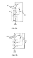
- FIG. 1A is a circuit diagram of a radio frequency interference suppression circuit in an embodiment of the present invention.
- FIG. 1B is a detail diagram of the radio frequency interference suppression circuit in an embodiment of the present invention.
- FIG. 1C is a diagram of the first switch, the driving circuit, the reference ground end and the high frequency differential mode loop in an embodiment of the present invention
- FIG. 2 is a diagram of a frequency response of the RFI in an embodiment of the present invention.
- FIG. 3A to FIG. 3E are detail circuit diagrams of the impedance unit in different embodiments of the present invention.
- FIG. 4A to FIG. 4H are diagrams of the package structure of the first switch, the driving circuit and the impedance unit in different embodiments of the present invention.
- FIG. 5A to FIG. 5D are diagrams of the package structure of the first switch, the driving circuit, the impedance unit and the capacitor branches in different embodiments of the present invention.
- FIG. 6A to FIG. 6C are diagrams of a RFI suppression circuit in different embodiments of the present invention.
- FIG. 7A to FIG. 7E are diagrams of a RFI suppression circuit in different embodiments of the present invention.
- FIG. 8A to FIG. 8B are diagrams of a RFI suppression circuit in different embodiments of the present invention.
- FIG. 9A to FIG. 9B are diagrams of a RFI suppression circuit in different embodiments of the present invention.
- FIG. 10A to FIG. 10B are diagrams of a RFI suppression circuit in different embodiments of the present invention.
- FIG. 11 is a diagram of a RFI suppression circuit in an embodiment of the present invention.
- FIG. 12 is a circuit diagram of a main power circuit of a primary/secondary side isolated type in an embodiment of the present invention.
- FIG. 13 is a diagram of a RFI suppression circuit in an embodiment of the present invention.
- FIG. 14 is a diagram of a RFI suppression circuit in an embodiment of the present invention.
- FIG. 15A and FIG. 15B are diagrams of the frequency response of the RFI in an embodiment of the present invention.
- FIG. 16 is a diagram of the frequency response of the RFI in an embodiment of the present invention.
- FIG. 17 is a diagram of an equivalent delivering model of the differential mode loop.
- FIG. 1A is a circuit diagram of a radio frequency interference suppression circuit 1 in an embodiment of the present invention.
- FIG. 1B is a detail diagram of the radio frequency interference suppression circuit 1 in an embodiment of the present invention.
- the radio frequency interference suppression circuit 1 includes a reference ground end GND, a main power circuit 10 , a driving circuit 12 and an impedance unit 14 .
- the main power circuit 10 can be a non-isolated converter circuit or an isolated converter circuit.
- the main power circuit 10 exemplarily illustrated in FIG. 1B is a boost converter, which is a kind of non-isolated converter circuit.
- the main power circuit 10 of the present invention is not limited thereto.
- the main power circuit 10 includes a first switch. In FIG. 1A , only one first switch 100 is exemplarily illustrated. In other embodiments, the main power circuit 10 may include a multiple of first switches.
- the first switch 100 includes a control end G, a first end D and a second end S.
- the first switch 100 can be implemented by a semiconductor field-effect transistor (MOSFET) as illustrated in FIG. 1B .
- the control end G is the gate, the first end D is the drain and the second end S is the source.
- the first switch 100 can be implemented by an insulated gate bipolar transistor (IGBT) or a bipolar junction transistor (BJT). Under such a condition, the control end G is the base, the first end D is the collector and the second end S is the emitter.
- IGBT insulated gate bipolar transistor
- BJT bipolar junction transistor
- the driving circuit 12 is coupled to the control end G and the second end S of the first switch 100 .
- the driving circuit 12 is disposed according to the number of the first switch 100 .
- one driving circuit 12 can be electrically coupled to a multiple of first switches to drive the first switches, depending on different applications.
- the driving circuit 12 generates a driving signal Drive. When the driving signal Drive is at a high state, the first switch 100 is turned on and is conducted between the first end D and the second end S. When the driving signal Drive is at a low state, the first switch 100 is turned off and is disconnected between the first end D and the second end S. Based on the turn-on and the turn-off of the first switch 100 between the first end D and the second end S, the main power circuit 10 converts a first power signal V 1 to a second power signal V 2 as illustrated in FIG. 1 B.
- the impedance unit 14 is formed between the second end S of the first switch 100 and the reference ground end GND. As compared to the other switches in the main power circuit 10 , minimal impedance is presented between the second end S and the reference ground end GND.
- the switch 100 is the first switch of the main power circuit 10 that has a path that has the minimal impedance between the second end S and the reference ground end GND, such as the path 16 illustrated in FIG. 1A and FIG. 1B .
- FIG. 1C is a diagram of the first switch 100 , the driving circuit 12 , the reference ground end GND and the high frequency differential mode loop 110 in an embodiment of the present invention.
- the high frequency differential mode loop 110 is an equivalent loop of the main power circuit 10 under the high frequency operation.
- the turn-on and turn-off of various switches in the main power circuit 10 cause instant changes of the current and voltage to form the differential mode interference source.
- the interference signal passes through the parasitic impedance in the return path of the high frequency differential mode loop 110 , a high frequency voltage drop is generated to become the common mode interference voltage and form the common mode interference current at the same time.
- the condition of the radio frequency interference is thus generated due to the high frequency voltage drop on the high frequency differential mode loop 110 .
- the impedance unit 14 has an impedance value not lower than 0.6 Ohm during a radiation frequency band of 30 mega hertz (MHz) to 1000 MHz. Since the impedance unit 14 is disposed between the second end S of the first switch 100 and the reference ground end GND, which is not in the driving loop formed by the driving circuit 12 and the first switch 100 , the driving speed is not affected, and the low loss characteristic of the components is maintained. However, the disposition of the impedance unit 14 increases the impedance value in the high frequency differential mode loop 110 and further decreases a high frequency voltage drop of the parasitic impedance of the high frequency differential return path. The condition of RFI is suppressed.
- FIG. 2 is a diagram of a frequency response of the RFI in an embodiment of the present invention.
- the x-axis is the frequency of the RFI signal in the unit of Hertz.
- the y-axis is the intensity of the RFI signal in the unit of dB.
- the dashed line illustrates the condition of having no impedance unit such that only the parasitic impedance of 0.03 nH is presented in the path 16 .
- the thinner line illustrates the condition of adding the impedance unit 14 to have the impedance value of 0.3 nH.
- the thicker line illustrates the condition of adding the impedance unit 14 to have the impedance value of 3 nH.
- FIG. 3A to FIG. 3E are detail circuit diagrams of the impedance unit 14 in different embodiments of the present invention.
- the impedance unit 14 can include a multiple of impedance components such as a resistive component R, an inductive component L, a capacitive component C or a combination of the above.
- the impedance components can form networks connected in parallel, in series or in both parallel and serial.
- the impedance unit 14 includes the resistive component R, the inductive component L and the capacitive component C connected in parallel.
- the impedance unit 14 includes the resistive component R, the inductive component L and the capacitive component C connected in series.
- FIG. 3A the impedance unit 14 includes the resistive component R, the inductive component L and the capacitive component C connected in parallel.
- FIG. 3B the impedance unit 14 includes the resistive component R, the inductive component L and the capacitive component C connected in series.
- the impedance unit 14 includes a network of the resistive component R, the inductive component L and the capacitive component C connected in series, wherein the network is further connected to a capacitive component C 2 in parallel.
- the impedance unit 14 includes a network of the resistive component R and the inductive component L connected in series, wherein the network is further connected to the capacitive component C in parallel.
- the impedance unit 14 includes a network of the resistive component R and the capacitive component C connected in parallel, wherein the network is further connected to the inductive component L in series.
- the impedance unit 14 can include different numbers and the configurations of components. Other impedance components known by that those skilled in the art can be included as well.
- FIG. 4A to FIG. 4H are diagrams of the package structure of the first switch 100 , the driving circuit 12 and the impedance unit 14 in different embodiments of the present invention.
- the first switch 100 , the driving circuit 12 and the impedance unit 14 are disposed in a single package structure 4 as illustrated in FIG. 4A . In another embodiment, the first switch 100 and the impedance unit 14 are disposed in the package structure 4 while the driving circuit 12 is disposed outside of the package structure 4 as illustrated in FIG. 4B .
- the number of the impedance unit 14 can be more than one and can be connected in series. Further, the first switch 100 , the driving circuit 12 and the impedance unit 14 are disposed in a single package structure 4 as illustrated in FIG. 4C . In another embodiment, the first switch 100 and the impedance units 14 having the number more than two are disposed in the package structure 4 while the driving circuit 12 is disposed outside of the package structure 4 as illustrated in FIG. 4D .
- a multiple of first switches 100 connected in parallel can be disposed in a package structure and operate to be turned on or turned off simultaneously.
- two first switches 100 are connected in parallel and two corresponding driving circuits 12 are disposed.
- the two first switches 100 can share one impedance unit 14 .
- the two first switches 100 and the two driving circuits 12 are disposed in the package structure 4 while the impedance unit 14 is disposed outside of the package structure 4 .
- two impedance units 14 can be respectively disposed corresponding to the two first switches 100 and are both connected to the reference ground end GND as illustrated in FIG. 4F .
- the two first switches 100 , the two driving circuits 12 and the impedance unit 14 are disposed in the package structure 4 .
- a multiple of first switches 100 connected in series can be disposed in a package structure and operate to be turned on or turned off simultaneously.
- two first switches 100 are electrically coupled and two corresponding driving circuits 12 are disposed in the package structure 4 .
- the impedance unit 14 is disposed outside of the package structure 4 .
- an additional impedance unit 40 is electrically coupled between the two first switches 100 as illustrated in FIG. 4H .
- the two first switches 100 , the two driving circuits 12 and the impedance unit 14 are disposed in the package structure 4 .
- the reference ground end GND can be electrically coupled to other external circuits through the reference ground pin 42 of the package structure 4 , as illustrated in FIG. 4A to FIG. 4D .
- FIG. 5A to FIG. 5D are diagrams of the package structure of the first switch 100 , the driving circuit 12 , the impedance unit 14 and the capacitor branches in different embodiments of the present invention.
- the RFI suppression circuit 1 in FIG. 1 further includes the capacitor branches 50 A and 50 B illustrated in FIG. 5A .
- the capacitor branches 50 A and 50 B may include at least one high frequency capacitor.
- the impedance unit 14 includes the structure in FIG. 3D , i.e. a network including the resistive component R and the inductive component L connected in series and the capacitive component C connected to the network in parallel are included therein.
- One end of the capacitor branch 50 A is electrically coupled to an inner node N between the resistive component R and the inductive component L.
- the other end of the capacitor branch 50 A is electrically coupled to a circuit node of the main power circuit 1 , such as the first end D of the first switch 100 .
- One end of the capacitor branch 50 B is electrically coupled to a node between the impedance unit 14 and the reference ground end GND.
- the other end of the capacitor branch 50 B is electrically coupled to the first end D of the first switch 100 too.
- the circuit node of the main power circuit 10 that the capacitor branches 50 A and 50 B are electrically coupled to can be other near ground potential power bus.
- the first switch 100 can be disposed in a package structure while the capacitor branches 50 A and 50 B can be selectively disposed in the same package structure or outside of the package structure.
- a multiple of capacitor branches can be disposed corresponding to the impedance units 14 , such as the capacitor branches 50 A, 50 B and 50 C illustrated in FIG. 5B .
- One end of each of the capacitor branches 50 A and 50 B is electrically coupled to the nodes N 1 and N 2 between the impedance units 14 respectively.
- One end of the capacitor branch 50 C is electrically coupled to a node N 3 between the impedance units 14 and the reference ground end GND, the other end is electrically coupled to the first end D of the first switch 100 .
- the multiple of capacitor branches 50 A, 50 B and 50 C, the first switch 100 and the impedance units 14 can be disposed in the package structure 4 as illustrated in FIG. 4 .
- the driving circuit 12 can be either disposed in the package structure 4 or outside of the package structure 4 as illustrated in FIG. 5D .
- FIG. 6A to FIG. 6C are diagrams of a RFI suppression circuit 6 in different embodiments of the present invention.
- RFI suppression circuit 6 Most of the components in the RFI suppression circuit 6 are identical to those in the RFI suppression circuit 1 in FIG. 1B and include the main power circuit 10 in the configuration of the boost converter circuit, the driving circuit 12 and the reference ground end GND. As a result, the detail of the identical components is not described herein.
- the RFI suppression circuit 6 includes a multiple of impedance units 14 and a multiple corresponding capacitor branches.
- the capacitor branches 60 A, 60 B and 60 C are disposed correspondingly to the impedance units 14 .
- One end of each the capacitor branches 60 A and 60 B is electrically coupled to the nodes N 1 and N 2 between the impedance units 14 respectively.
- the other end of each of the capacitor branches 60 A and 60 B is electrically coupled to the output end O of the boost converter circuit.
- One end of the capacitor branch 60 C is electrically coupled to the node N 3 between the impedance units 14 and the reference ground end GND.
- the other end is electrically coupled to the output end O of the boost converter circuit.
- the capacitor branches 60 A, 60 B and 60 C are disposed correspondingly to the impedance units 14 .
- One end of each the capacitor branches 60 A and 60 B is electrically coupled to the nodes N 1 and N 2 between the impedance units 14 respectively.
- the other end of each of the capacitor branches 60 A and 60 B is electrically coupled to the input end IN of the boost converter circuit.
- One end of the capacitor branch 60 C is electrically coupled to the node N 3 between the impedance units 14 and the reference ground end GND.
- the other end is electrically coupled to the input end IN of the boost converter circuit.
- the connection methods in FIG. 6A and FIG. 6B can be integrated to dispose the capacitor branch. Taking FIG.
- the capacitor branches 60 A, 60 B and 60 C are electrically coupled to the output end O and the impedance units 14 as the method in FIG. 6A
- the capacitor branches 60 D, 60 E and 60 F are electrically coupled to the input end IN and the impedance units 14 as the method in FIG. 6B .
- FIG. 7A to FIG. 7E are diagrams of a RFI suppression circuit 7 in different embodiments of the present invention.
- the main power circuit 10 in the RFI suppression circuit 7 is a half bridge circuit.
- the main power circuit 10 includes an upper bridge 700 and a lower bridge 702 formed by the first switch 100 and a second switch 102 electrically coupled together.
- the type of the second switch also includes the MOSFET, IGBT and BJT.
- the impedance between the second terminal S of the first switch 100 in the lower bridge 702 and the reference ground end GND is lower than the impedance corresponding to the second switch 102 .
- the impedance unit 14 is disposed to be electrically coupled to the first switch 100 in the lower bridge 702 .
- the main power circuit includes two pairs of second switches 102 and the first switches 100 electrically coupled together to form the upper bridges 700 and 704 and the lower bridges 702 and 706 .
- the impedances of the second ends S of the first switches 100 in both the two lower bridges 702 and 706 and the reference ground end GND are the same, and such impedances are lower than those corresponding to the second switches 102 of the upper bridges 700 and 704 .
- the impedance units 14 are disposed to be electrically coupled to the first switches 100 in the lower bridges 702 and 706 .
- the main power circuit includes three pairs of second switches 102 and the first switches 100 electrically coupled together to form the upper bridges 700 , 704 and 708 and the lower bridges 702 , 706 and 710 .
- the impedances of the second ends S of the first switches 100 in the three lower bridges 702 , 706 and 710 and the reference ground end GND are the same, and such impedances are lower than those corresponding to the second switches 102 of the upper bridges 700 , 704 and 708 .
- the impedance units 14 are disposed to be electrically coupled to the first switches 100 in the lower bridges 702 , 706 and 710 .
- additional impedance units 720 can be added between the second switch 102 and the first switch 100 of the upper and lower bridges 700 and 702 to accomplish a better filtering and attenuation result.
- the capacitor branches 74 A, 74 B, 76 A and 76 B corresponding to the upper and the lower bridges can be combined with the topology in FIG. 7D to realize a multiple stages of filtering network.
- the combination and the package structure of the second switch, the impedance unit and the capacitor branch can be referred to the description related to the first switch.
- the difference of the second switch and the first switch is that the impedance of the second end of the second switch to the reference ground end is not to smallest impedance.
- FIG. 8A to FIG. 8B are diagrams of a RFI suppression circuit 8 in different embodiments of the present invention.
- the main power circuit 10 in the RFI suppression circuit 8 is a D-type three level bridge circuit.
- the first switch 100 (surrounded by think dashed frame) that is closest to the reference ground end GND has the minimal impedance as compared to the other second switches 102 .
- the impedance unit 14 is disposed to be electrically coupled to this closest first switch 100 .
- additional impedance units 800 can be added to be corresponding to the second switch 102 to accomplish a better filtering and attenuation result.
- the capacitor branches 80 A, 80 B, 80 C and 80 D can be combined with the topology in FIG. 8A to realize a multiple stages of filtering network.
- FIG. 9A to FIG. 9B are diagrams of a RFI suppression circuit 9 in different embodiments of the present invention.
- the main power circuit 10 in the RFI suppression circuit 9 is a T-type three level bridge circuit.
- the first switch 100 (surrounded by think dashed frame) that is closest to the reference ground end GND has the minimal impedance as compared to the other second switches 102 .
- the impedance unit 14 is disposed to be electrically coupled to this closest first switch 100 .
- additional impedance units 900 can be added to be corresponding to the second switch 102 to accomplish a better filtering and attenuation result.
- the capacitor branches 90 A, 90 B, 90 C and 90 D can be combined with the topology in FIG. 9A to realize a multiple stages of filtering network.
- FIG. 10A to FIG. 10B are diagrams of a RFI suppression circuit 1000 in different embodiments of the present invention.
- the main power circuit 10 in the RFI suppression circuit 1000 is a totem pole power factor correction circuit.
- the single type totem pole power factor correction circuit is illustrated in FIG. 10A .
- the first switch 100 (surrounded by think dashed frame) that is closest to the reference ground end GND has the minimal impedance as compared to the other second switches 102 .
- the impedance unit 14 is disposed to be electrically coupled to this closest first switch 100 .
- additional impedance units 1002 can be added to be corresponding to the second switch 102 to accomplish a better filtering and attenuation result.
- the capacitor branches 1004 A, 1004 B, 1004 C and 1004 D can be combined to realize a multiple stages of filtering network.
- the interleaving type totem pole power factor correction circuit is illustrated in FIG. 10B .
- the two first switches 100 (surrounded by think dashed frame) that are closest to the reference ground end GND has the minimal impedance as compared to the other second switches 102 .
- the impedance units 14 are correspondingly disposed to be electrically coupled to those closest first switches 100 .
- additional impedance units 1002 can be added to be corresponding to the second switch 102 to accomplish a better filtering and attenuation result.
- the capacitor branches 1004 A- 1004 D and 1006 A- 1006 D can be combined to realize a multiple stages of filtering network.
- FIG. 11 is a diagram of a RFI suppression circuit 1100 in an embodiment of the present invention.
- the main power circuit 10 in the RFI suppression circuit 1100 is a synchronous buck converter circuit.
- the first switch 100 (surrounded by think dashed frame) that is closest to the reference ground end GND has the minimal impedance as compared to the other second switches 102 .
- the impedance unit 14 is disposed to be electrically coupled to this closest first switch 100 .
- additional impedance units 1102 can be added to be corresponding to the second switch 102 to accomplish a better filtering and attenuation result.
- the capacitor branches 1104 A- 1104 D can be combined to realize a multiple stages of filtering network.
- FIG. 12 is a circuit diagram of a main power circuit 10 of a primary/secondary side isolated type in an embodiment of the present invention.
- a high frequency voltage drop Vac is generated between the nodes A and C due to the high frequency current passing through the parasitic impedance relative to the reference ground of the primary side.
- a high frequency voltage drop Vbd is generated between the nodes B and D due to the presence of the parasitic impedance relative to the reference ground of the secondary ground.
- a capacitor Cy0 or other kind impedance is presented between the reference grounds of the primary side and the secondary side to decrease the common mode electromagnetic interference.
- a high frequency voltage drop Vab is generated between nodes A and B on the path corresponding to the impedance Cy0.
- the high frequency voltage drop equivalent to Vac+Vab+Vbd is presented between the primary input wire 1204 and the secondary output wire 1206 and excites the primary input wire 1204 and the secondary output wire 1206 to form a delivering antenna to generate RFI.
- FIG. 13 is a diagram of a RFI suppression circuit 1300 in an embodiment of the present invention.
- the main power circuit 10 in the RFI suppression circuit 1300 is a fly-back converter.
- the first switch 100 (surrounded by think dashed frame) in the primary side that is closest to the reference ground end GND has the minimal impedance as compared to the other second switches 102 .
- the impedance unit 14 is disposed to be electrically coupled to this closest first switch 100 .
- additional impedance unit 14 can be added to be corresponding to the second switch 102 to accomplish a better filtering and attenuation result.
- the capacitor branches 1302 A, 1302 B and 1302 C can be combined to realize a multiple stages of filtering network.
- capacitor branches One end of these capacitor branches is coupled to a node of one end of the impedance unit 14 , and the other end of these capacitor branches can be coupled to either the constant voltage node of the primary side or the constant voltage node of the secondary side.
- the constant voltage node refers to a circuit node that has no high frequency voltage deviation and always has a constant voltage relative to a stable reference ground, such as the positive and negative bus of the primary input side or the secondary output side.
- the capacitor branches are coupled to the constant voltage node P of the secondary side to decrease the high frequency voltage drop between the primary and the secondary sides to decrease the RFI of the converter.
- FIG. 14 is a diagram of a RFI suppression circuit 1400 in an embodiment of the present invention.
- the main power circuit 10 in the RFI suppression circuit 1400 is a LLC converter.
- the first switch 100 (surrounded by think dashed frame) in the primary side that is closest to the reference ground end GND has the minimal impedance as compared to the other second switches 102 .
- the impedance unit 14 is disposed to be electrically coupled to this closest first switch 100 .
- additional impedance unit 14 can be added to be corresponding to the second switch 102 to accomplish a better filtering and attenuation result.
- the capacitor branches 1402 A, 1402 B and 1402 C can be combined to realize a multiple stages of filtering network.
- the constant voltage node refers to a circuit node that has no high frequency voltage deviation and always has a constant voltage relative to a stable reference ground, such as the positive and negative bus of the primary input side or the secondary output side.
- the capacitor branches are coupled the constant voltage node P of the secondary side is coupled to decrease the high frequency voltage drop between the primary and the secondary sides to decrease the RFI of the converter.
- FIG. 15A and FIG. 15B are diagrams of the frequency response of the RFI in an embodiment of the present invention.
- the x-axis is the frequency of the RFI signal in the unit of mega Hertz.
- the y-axis is the intensity of the RFI signal in the unit of dB.
- the following description uses the boost converter circuit as an
- the dashed line illustrates the condition of having no impedance unit such that only the parasitic impedance of 0.03 nH is presented in the path 16 .
- the thinner line illustrates the condition of adding the impedance unit 14 to have the impedance value of 0.3 nH.
- the thicker line illustrates the condition of adding the impedance unit 14 to have the impedance value of 3 nH.
- the parasitic inductance of the wires is about 5 nH and the mutual inductance between each of the loop wires is not neglectable.
- the changes of the impedance unit 14 result in the corresponding changes of the high frequency voltage drop.
- FIG. 15A and FIG. 15B when the impedance value of the added impedance unit 14 (taking the inductive or the resistive impedance unit as an example) gradually increases and when the high frequency decoupling capacitors are incorporated, a multiple filtering stages around the source are formed such that there is 10 dB to 30 dB of attenuation during the radio frequency band in the curve of the frequency response.
- the curves from top to down as indicated by the arrow with the dashed line correspond to the frequency responses when the added inductor has the impedance values of 1 nH, 5 nH, 9 nH, 13 nH and 17 nH respectively, wherein the combined capacitor is 10 nF. If the curve corresponding to the added inductor having the impedance of 1 nH is used as an initial object to be compared, it is obvious that the curve of the frequency response gradually decreases along with the increment of the inductance of the added inductor. A larger amount of attenuation ranging from 5 dB to 30 dB is obtained within the frequency band from 40 MHz to 100 MHz.
- the curves from top to down as indicated by the arrow with the dashed line correspond to the frequency responses when the added resistance has the impedance values of 0.1 Ohm to 100 Ohm (the impedance values are 0.1 Ohm, 0.3 Ohm, 1 Ohm, 3 Ohm, 10 Ohm, 30 Ohm and 100 Ohm respectively), wherein the combined capacitor is 10 nF.
- the curve corresponding to the added resistor having the impedance of 0.1 Ohm is used as an initial object to be compared, it is obvious that the curve of the frequency response gradually decreases along with the increment of the resistance of the added resistor. A larger amount of attenuation ranging from 5 dB to 40 dB is obtained within the frequency band from 30 MHz to 100 MHz.
- the frequency response characteristic can be adjusted by adjusting a combination of the parameters of the impedance unit 14 and the high frequency capacitor to bring the attenuation specifically at other frequency bands of the frequency response curve.
- FIG. 16 is a diagram of the frequency response of the RFI in an embodiment of the present invention.
- the x-axis is the frequency of the RFI signal in the unit of mega Hertz.
- the y-axis is the intensity of the RFI signal in the unit of dB.
- the parasitic inductance of the wire is smaller than 1 nH and the coupling coefficients between the loops having a smaller size become 1/10 of the original value or an even smaller amount.
- the added impedance unit 14 in combination with the high frequency capacitor branch mentioned above result in an even greater attenuation of the high frequency excitation between the equivalent antennas of the input and output wires.
- the curves from top to down as indicated by the arrow with the dashed line correspond to the frequency responses when the added inductor has the impedances of 3 nH, 6 nH, 9 nH, 12 nH, 15 nH and 18 nH respectively, wherein the combined capacitor is 1 nF. If the curve corresponding to the added inductor having the impedance of 3 nH is used as an initial object to be compared, it is obvious a larger amount of attenuation ranging from 5 dB to 15 dB is obtained within the frequency band from 30 MHz to 47 MHz. A larger amount of attenuation ranging from 5 dB to 30 dB is obtained within the frequency band from 100 MHz to 200 MHz.
- the result in FIG. 16 reveals that when the circuit uses advanced package technology to make the parasitic parameters even smaller, a better high frequency attenuation result can be obtained by using a combination of the impedance unit 14 and capacitor having an even smaller values.
Landscapes
- Engineering & Computer Science (AREA)
- Power Engineering (AREA)
- Physics & Mathematics (AREA)
- Electromagnetism (AREA)
- Electronic Switches (AREA)
- Amplifiers (AREA)
Applications Claiming Priority (3)
| Application Number | Priority Date | Filing Date | Title |
|---|---|---|---|
| CN201510622396.8A CN106558982B (zh) | 2015-09-25 | 2015-09-25 | 射频干扰抑制电路 |
| CN201510622396.8 | 2015-09-25 | ||
| CN201510622396 | 2015-09-25 |
Publications (2)
| Publication Number | Publication Date |
|---|---|
| US20170093275A1 US20170093275A1 (en) | 2017-03-30 |
| US9806602B2 true US9806602B2 (en) | 2017-10-31 |
Family
ID=58227217
Family Applications (1)
| Application Number | Title | Priority Date | Filing Date |
|---|---|---|---|
| US15/272,420 Active US9806602B2 (en) | 2015-09-25 | 2016-09-21 | Radio frequency interference suppression circuit |
Country Status (3)
| Country | Link |
|---|---|
| US (1) | US9806602B2 (zh) |
| CN (1) | CN106558982B (zh) |
| TW (1) | TWI561002B (zh) |
Families Citing this family (4)
| Publication number | Priority date | Publication date | Assignee | Title |
|---|---|---|---|---|
| CN104753338B (zh) * | 2013-12-25 | 2018-03-23 | 台达电子企业管理(上海)有限公司 | 电力电子电路与功率模块 |
| EP3813099B1 (en) | 2016-06-15 | 2022-08-03 | Watlow Electric Manufacturing Company | Power converter for a thermal system |
| US11277912B2 (en) * | 2018-02-01 | 2022-03-15 | Delta Electronics (Shanghai) Co., Ltd | System of providing power |
| CN110112905A (zh) | 2018-02-01 | 2019-08-09 | 台达电子企业管理(上海)有限公司 | 主板上芯片供电系统 |
Citations (8)
| Publication number | Priority date | Publication date | Assignee | Title |
|---|---|---|---|---|
| US6819744B1 (en) * | 1999-09-30 | 2004-11-16 | Telcordia Technologies, Inc. | System and circuitry for measuring echoes on subscriber loops |
| US20060164868A1 (en) * | 2002-10-16 | 2006-07-27 | Rudolf Weber | Capacitively coupled power supply |
| US20080143285A1 (en) * | 2006-11-21 | 2008-06-19 | Lucas Donald J | RFI/EMI filter for variable frequency motor drive system |
| US8222965B1 (en) * | 2009-09-18 | 2012-07-17 | Dust Networks, Inc. | Radio frequency modulator |
| US20150180351A1 (en) * | 2013-12-25 | 2015-06-25 | Delta Electronics (Shanghai) Co., Ltd. | Power electronic circuit and power module |
| US20160164448A1 (en) * | 2014-12-09 | 2016-06-09 | Johnson Controls Technology Company | Electromagnetic compatibility filter |
| US20170054294A1 (en) * | 2015-08-18 | 2017-02-23 | Virginia Tech Intellectual Properties, Inc. | Modular multilevel converter capacitor voltage ripple reduction |
| US20170149240A1 (en) * | 2015-11-25 | 2017-05-25 | Freescale Semiconductor, Inc. | Single inductor, multiple output dc-dc converter |
Family Cites Families (5)
| Publication number | Priority date | Publication date | Assignee | Title |
|---|---|---|---|---|
| DE2709579C2 (de) * | 1976-03-05 | 1985-06-27 | Sanyo Electric Co., Ltd., Moriguchi, Osaka | VHF-Tuner |
| DE3139673C2 (de) * | 1981-10-06 | 1985-04-25 | Brown, Boveri & Cie Ag, 6800 Mannheim | Schaltungsanordnung zur Funkentstörung bei Steuergeräten nach dem Phasenanschnittprinzip |
| US5504395A (en) * | 1993-03-08 | 1996-04-02 | Beacon Light Products, Inc. | Lamp bulb having integrated RFI suppression and method of restricting RFI to selected level |
| CA2479685A1 (en) * | 2002-03-18 | 2003-10-02 | Ems Technologies, Inc. | Passive intermodulation interference control circuits |
| CN104079162A (zh) * | 2014-06-10 | 2014-10-01 | 南京航空航天大学 | 功率变换器及该功率变换器共模emi噪声源抑制方法 |
-
2015
- 2015-09-25 CN CN201510622396.8A patent/CN106558982B/zh active Active
- 2015-11-26 TW TW104139304A patent/TWI561002B/zh active
-
2016
- 2016-09-21 US US15/272,420 patent/US9806602B2/en active Active
Patent Citations (8)
| Publication number | Priority date | Publication date | Assignee | Title |
|---|---|---|---|---|
| US6819744B1 (en) * | 1999-09-30 | 2004-11-16 | Telcordia Technologies, Inc. | System and circuitry for measuring echoes on subscriber loops |
| US20060164868A1 (en) * | 2002-10-16 | 2006-07-27 | Rudolf Weber | Capacitively coupled power supply |
| US20080143285A1 (en) * | 2006-11-21 | 2008-06-19 | Lucas Donald J | RFI/EMI filter for variable frequency motor drive system |
| US8222965B1 (en) * | 2009-09-18 | 2012-07-17 | Dust Networks, Inc. | Radio frequency modulator |
| US20150180351A1 (en) * | 2013-12-25 | 2015-06-25 | Delta Electronics (Shanghai) Co., Ltd. | Power electronic circuit and power module |
| US20160164448A1 (en) * | 2014-12-09 | 2016-06-09 | Johnson Controls Technology Company | Electromagnetic compatibility filter |
| US20170054294A1 (en) * | 2015-08-18 | 2017-02-23 | Virginia Tech Intellectual Properties, Inc. | Modular multilevel converter capacitor voltage ripple reduction |
| US20170149240A1 (en) * | 2015-11-25 | 2017-05-25 | Freescale Semiconductor, Inc. | Single inductor, multiple output dc-dc converter |
Also Published As
| Publication number | Publication date |
|---|---|
| CN106558982A (zh) | 2017-04-05 |
| CN106558982B (zh) | 2019-03-15 |
| US20170093275A1 (en) | 2017-03-30 |
| TW201713038A (zh) | 2017-04-01 |
| TWI561002B (en) | 2016-12-01 |
Similar Documents
| Publication | Publication Date | Title |
|---|---|---|
| US9806602B2 (en) | Radio frequency interference suppression circuit | |
| US11062837B2 (en) | Planar transformer, power conversion circuit, and adapter | |
| US9711486B2 (en) | Stacked semiconductor device | |
| US10491180B2 (en) | Board-type noise filter and electronic device | |
| TWI262588B (en) | Static electricity protective circuit and high-frequency circuit apparatus incorporating the same | |
| US10498218B2 (en) | Switching circuit apparatus and electric power converter capable of reducing common mode noise in asymmetric circuit | |
| US10886730B2 (en) | Filter having an ESD protection device | |
| CN103635995B (zh) | 保护电路 | |
| JP3094739U (ja) | 集積回路チップのノイズを低減するための装置 | |
| CN111697933A (zh) | 栅极路径中具有扼流圈的并联功率半导体 | |
| US6950291B1 (en) | Electromagnetic interference shielding for small magnetic devices | |
| JP6611999B1 (ja) | 空気調和機 | |
| US9941227B2 (en) | Impedance matching configuration | |
| WO2021049091A1 (ja) | 電力変換装置、鉄道車両電気システム | |
| CN106470014B (zh) | 具有谐波防止电路的输出阻抗匹配网络 | |
| JP2008198761A (ja) | 半導体装置 | |
| CN108736579A (zh) | 无线电能发射电路 | |
| WO2017043611A1 (ja) | パワーデバイス | |
| US11632041B2 (en) | Power semiconductor module | |
| US20070109065A1 (en) | Methods and apparatus for the reduction of local oscillator pulling in zero intermediate frequency transmitters | |
| CN112189306A (zh) | 噪声滤波器 | |
| CN114301289B (zh) | 电气设备以及电力变换装置 | |
| CN220210240U (zh) | 一种滤波电路和开关电源 | |
| KR101601829B1 (ko) | 고출력 반도체 소자 패키지 | |
| JP2022547129A (ja) | 過渡ノイズ低減フィルタリングシステム |
Legal Events
| Date | Code | Title | Description |
|---|---|---|---|
| AS | Assignment |
Owner name: DELTA ELECTRONICS, INC., TAIWAN Free format text: ASSIGNMENT OF ASSIGNORS INTEREST;ASSIGNORS:XIE, YI-CONG;ZHOU, MIN;WU, RUI;AND OTHERS;REEL/FRAME:039822/0556 Effective date: 20160804 |
|
| STCF | Information on status: patent grant |
Free format text: PATENTED CASE |
|
| MAFP | Maintenance fee payment |
Free format text: PAYMENT OF MAINTENANCE FEE, 4TH YEAR, LARGE ENTITY (ORIGINAL EVENT CODE: M1551); ENTITY STATUS OF PATENT OWNER: LARGE ENTITY Year of fee payment: 4 |