US9800271B2 - Error correction and decoding - Google Patents
Error correction and decoding Download PDFInfo
- Publication number
- US9800271B2 US9800271B2 US14/852,988 US201514852988A US9800271B2 US 9800271 B2 US9800271 B2 US 9800271B2 US 201514852988 A US201514852988 A US 201514852988A US 9800271 B2 US9800271 B2 US 9800271B2
- Authority
- US
- United States
- Prior art keywords
- output
- error
- double
- input
- error location
- Prior art date
- Legal status (The legal status is an assumption and is not a legal conclusion. Google has not performed a legal analysis and makes no representation as to the accuracy of the status listed.)
- Expired - Fee Related, expires
Links
Images


Classifications
-
- H—ELECTRICITY
- H03—ELECTRONIC CIRCUITRY
- H03M—CODING; DECODING; CODE CONVERSION IN GENERAL
- H03M13/00—Coding, decoding or code conversion, for error detection or error correction; Coding theory basic assumptions; Coding bounds; Error probability evaluation methods; Channel models; Simulation or testing of codes
- H03M13/61—Aspects and characteristics of methods and arrangements for error correction or error detection, not provided for otherwise
- H03M13/615—Use of computational or mathematical techniques
- H03M13/616—Matrix operations, especially for generator matrices or check matrices, e.g. column or row permutations
-
- G—PHYSICS
- G06—COMPUTING OR CALCULATING; COUNTING
- G06F—ELECTRIC DIGITAL DATA PROCESSING
- G06F11/00—Error detection; Error correction; Monitoring
- G06F11/07—Responding to the occurrence of a fault, e.g. fault tolerance
- G06F11/08—Error detection or correction by redundancy in data representation, e.g. by using checking codes
- G06F11/10—Adding special bits or symbols to the coded information, e.g. parity check, casting out 9's or 11's
- G06F11/1008—Adding special bits or symbols to the coded information, e.g. parity check, casting out 9's or 11's in individual solid state devices
- G06F11/1012—Adding special bits or symbols to the coded information, e.g. parity check, casting out 9's or 11's in individual solid state devices using codes or arrangements adapted for a specific type of error
-
- H—ELECTRICITY
- H03—ELECTRONIC CIRCUITRY
- H03M—CODING; DECODING; CODE CONVERSION IN GENERAL
- H03M13/00—Coding, decoding or code conversion, for error detection or error correction; Coding theory basic assumptions; Coding bounds; Error probability evaluation methods; Channel models; Simulation or testing of codes
- H03M13/03—Error detection or forward error correction by redundancy in data representation, i.e. code words containing more digits than the source words
- H03M13/05—Error detection or forward error correction by redundancy in data representation, i.e. code words containing more digits than the source words using block codes, i.e. a predetermined number of check bits joined to a predetermined number of information bits
- H03M13/13—Linear codes
- H03M13/15—Cyclic codes, i.e. cyclic shifts of codewords produce other codewords, e.g. codes defined by a generator polynomial, Bose-Chaudhuri-Hocquenghem [BCH] codes
- H03M13/151—Cyclic codes, i.e. cyclic shifts of codewords produce other codewords, e.g. codes defined by a generator polynomial, Bose-Chaudhuri-Hocquenghem [BCH] codes using error location or error correction polynomials
- H03M13/152—Bose-Chaudhuri-Hocquenghem [BCH] codes
-
- H—ELECTRICITY
- H03—ELECTRONIC CIRCUITRY
- H03M—CODING; DECODING; CODE CONVERSION IN GENERAL
- H03M13/00—Coding, decoding or code conversion, for error detection or error correction; Coding theory basic assumptions; Coding bounds; Error probability evaluation methods; Channel models; Simulation or testing of codes
- H03M13/03—Error detection or forward error correction by redundancy in data representation, i.e. code words containing more digits than the source words
- H03M13/05—Error detection or forward error correction by redundancy in data representation, i.e. code words containing more digits than the source words using block codes, i.e. a predetermined number of check bits joined to a predetermined number of information bits
- H03M13/13—Linear codes
- H03M13/15—Cyclic codes, i.e. cyclic shifts of codewords produce other codewords, e.g. codes defined by a generator polynomial, Bose-Chaudhuri-Hocquenghem [BCH] codes
- H03M13/151—Cyclic codes, i.e. cyclic shifts of codewords produce other codewords, e.g. codes defined by a generator polynomial, Bose-Chaudhuri-Hocquenghem [BCH] codes using error location or error correction polynomials
- H03M13/1575—Direct decoding, e.g. by a direct determination of the error locator polynomial from syndromes and subsequent analysis or by matrix operations involving syndromes, e.g. for codes with a small minimum Hamming distance
-
- H—ELECTRICITY
- H03—ELECTRONIC CIRCUITRY
- H03M—CODING; DECODING; CODE CONVERSION IN GENERAL
- H03M13/00—Coding, decoding or code conversion, for error detection or error correction; Coding theory basic assumptions; Coding bounds; Error probability evaluation methods; Channel models; Simulation or testing of codes
- H03M13/61—Aspects and characteristics of methods and arrangements for error correction or error detection, not provided for otherwise
- H03M13/615—Use of computational or mathematical techniques
- H03M13/617—Polynomial operations, e.g. operations related to generator polynomials or parity-check polynomials
-
- H—ELECTRICITY
- H03—ELECTRONIC CIRCUITRY
- H03M—CODING; DECODING; CODE CONVERSION IN GENERAL
- H03M13/00—Coding, decoding or code conversion, for error detection or error correction; Coding theory basic assumptions; Coding bounds; Error probability evaluation methods; Channel models; Simulation or testing of codes
- H03M13/65—Purpose and implementation aspects
- H03M13/6502—Reduction of hardware complexity or efficient processing
Definitions
- Various embodiments described herein relate to error correction, and more particularly, to single-bit and multiple-bit error correction.
- More powerful error detecting and correcting schemes have been devised to address the problem of multiple-bit errors.
- schemes such as double error correcting-triple error detecting (DEC-TED) have been devised which would provide more powerful error correcting capabilities than conventional SEC-DED schemes.
- the area of circuitry typically required for DEC-TED would be much larger than the area required for SEC-DED.
- conventional DEC-TED circuitry typically consumes more power and results in longer latency or time delay than conventional SEC-DED circuitry. For example, when DEC-TED circuitry is utilized to correct a single error, power consumption and time delay would be much greater than SEC-DED circuitry.
- pure combinational circuits implementing error correcting codes for single- or multiple-bit error correction may typically consume large amounts of dynamic power when the input changes due to invalid transitions in error location decoding. It would be desirable to reduce the amount of power consumption required for error detection and correction, especially for multiple-bit error detection and correction in low-power integrated circuit devices such as low-power memory chips.
- Exemplary embodiments of the disclosure are directed to apparatus and methods of double error correction in memories with reduced power consumption.
- an error detection and correction apparatus comprising: a single error location decoder configured to locate single errors in input data; a double error location decoder configured to locate double errors in the input data; and an error corrector coupled to the single error location decoder and the double error location decoder to generate corrected output data.
- an error detection and correction apparatus comprising: means for single error location decoding to locate single errors in input data; means for double error location decoding to locate double errors in the input data; and means for correcting errors to generate corrected output data based on the single errors and the double errors.
- an error detection and correction apparatus comprising: logic configured to locate single errors in input data; logic configured to locate double errors in the input data; and logic configured to generate corrected output data based on the single errors and the double errors.
- a memory comprising: a memory cell; and an error detection and correction apparatus coupled to receive input data from the memory cell and to transmit corrected output data to the memory cell, the error detection and correction apparatus comprising: a single error location decoder configured to locate single errors in input data; a double error location decoder configured to locate double errors in the input data; and an error corrector coupled to the single error location decoder and the double error location decoder to generate corrected output data.
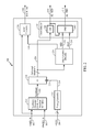
- FIG. 1 is a block diagram illustrating an embodiment of an error detection and correction apparatus.
- FIG. 2 is a block diagram illustrating another embodiment of an error detection and correction apparatus having a flip-flop and a timing controller.
- FIG. 3 is a block diagram illustrating an embodiment of a delay line as a timing controller in the embodiment of the error correcting and decoding apparatus of FIG. 2 .
- FIG. 4 is a block diagram illustrating yet another embodiment of an error detection and correction apparatus having flip-flops, a timing controller, separate single error correction (SEC) and double error correction (DEC) error location decoders, a multiplexer, and a flag generator.
- SEC single error correction
- DEC double error correction
- FIG. 5 is a block diagram illustrating an embodiment of an error detection and correction apparatus with logic configured to perform error detection and correction functions.
- FIG. 6 is a block diagram illustrating an embodiment of a memory device in which error detection and correction apparatus may be implemented.
- FIG. 1 is a block diagram illustrating an embodiment of an error detection and correction apparatus 100 having a data input (databit_in) 102 , an error check input (checkbit_in) 104 , and a corrected data output (databit_out) 106 .
- Such an error correcting code decoder may be implemented in various digital apparatus or devices for correcting data errors, for example, in memory devices such as spin-transfer torque magnetic random access memories (STT-MRAMs). It will be appreciated that the error correcting code decoder according to embodiments of the disclosure may also be used in various other apparatus or devices by persons skilled in the art. Referring to FIG.
- the error detection and correction apparatus 100 includes a syndrome generator 108 which is configured to receive the data input (databit_in) 102 and the error check input (checkbit_in) 104 .
- the syndrome generator 108 is capable of generating a first vector signal output (S 0 ), a second vector signal output (S 1 ) and a third vector signal output (S 3 ) in response to the data input (databit_in) 102 and the error check input (checkbit_in) 104 .
- the syndrome generator 108 comprises a parity-check matrix decoder, and the error check input (checkbit_in) 104 comprises a parity-check bit input.
- a syndrome generator 108 may be constructed by using one of many known error correcting codes (ECCs).
- the parity-check matrix decoder may comprise an XOR-tree based parity-check matrix decoder.
- the syndrome generator 108 may be constructed by implementing an ECC such as a double error correcting-triple error detecting (DEC-TED) Bose-Chaudhuri-Hocquenghem (BCH) code where a is a primitive element in the Galois field GF(2 n ):
- the error detection and correction apparatus 100 also includes a controller 110 which is configured to receive the first vector signal output (S 0 ), the second vector signal output (S 1 ) and the third vector signal output (S 3 ) from the syndrome generator 108 , and to generate a single error correction output (SEC_output) and a double error correction output (DEC_output) based on at least two of the three vector signals S 0 , S 1 and S 3 from the syndrome generator 108 .
- a controller 110 which is configured to receive the first vector signal output (S 0 ), the second vector signal output (S 1 ) and the third vector signal output (S 3 ) from the syndrome generator 108 , and to generate a single error correction output (SEC_output) and a double error correction output (DEC_output) based on at least two of the three vector signals S 0 , S 1 and S 3 from the syndrome generator 108 .
- the controller 110 is implemented to generate the single error correction output (SEC_output) and the double error correction output (DEC_output), which are transmitted to the inputs of a single error correction (SEC) error location decoder 118 and a double error correction (DEC) error location decoder 120 , respectively.
- SEC single error correction
- DEC double error correction
- the SEC error location decoder 118 and the DEC error location decoder 120 will be described in further detail below.
- the single error correction output (SEC_output) and the double error correction output (DEC_output) of the controller 110 are set to satisfy the above conditions. For example, if the first vector signal output (S 0 ) from the syndrome generator 108 is one, which means that the data input is assumed to have a single error, then the double error correction output (DEC_output) of the controller 110 is a zero vector. In contrast, if the first vector signal output (S 0 ) from the syndrome generator 108 is zero, which means that the data input is assumed to have a double error, then the single error correction output (SEC_output) of the controller is a zero vector.
- the error detection and correction apparatus 100 further includes a double error detector 112 which has inputs coupled to receive the first vector signal output (S 0 ), the second vector signal output (S 1 ) and the third vector signal output (S 3 ) from the syndrome generator 108 , and an output that generates a double error detection output (AL_DED) 114 based on the three vector signals S 0 , S 1 and S 3 received from the syndrome generator 108 .
- a double error detector 112 which has inputs coupled to receive the first vector signal output (S 0 ), the second vector signal output (S 1 ) and the third vector signal output (S 3 ) from the syndrome generator 108 , and an output that generates a double error detection output (AL_DED) 114 based on the three vector signals S 0 , S 1 and S 3 received from the syndrome generator 108 .
- a flag generator 116 is provided in the error detection and correction apparatus 100 as illustrated in FIG. 1 .
- the flag generator 116 is provided to determine the number of errors from zero error to triple error.
- the flag generator 116 generates a two-bit variable called an error flag (error_flag) 122 , which is output from the error detection and correction apparatus 100 as a two-bit indicator of zero error, single error, double error or triple error.
- error_flag error flag
- error flag (error_flag) 122 may be determined based on the double error detection output (AL_DED) 114 from the double error detector 112 and the first vector signal output (S 0 ) from the syndrome generator 108 :
- the SEC error location decoder 118 is provided to locate single errors and the DEC error location decoder 120 is provided to locate double errors.
- the SEC error location decoder 118 is coupled to receive the single error correction output (SEC_output) from the controller 110 and outputs a single error location decoder output (e_sec) 124 based on the SEC_output from the controller 110 .
- the DEC error location decoder 120 is coupled to receive the double error correction output (DEC_output) from the controller 110 and outputs a double error location decoder output (e_dec) 126 based on the DEC_output from the controller 110 .
- a multiplexer 128 is provided in the error detection and correction apparatus 100 to generate a multiplexer output 130 .
- the multiplexer 128 comprises a 2:1 multiplexer having a first input coupled to the single error location decoder output (e_sec) 124 , a second input coupled to the double error location decoder output (e_dec) 126 , and a multiplexer output 130 to output either the single error location decoder output (e_sec) or the double error location decoder output (e_dec) based on a control input 132 .
- control input 132 for the multiplexer 128 is an input that receives the logical complement of the double error detection output (AL_DED) from the double error detector 112 .
- control signal which is ( ⁇ AL_DED)
- the control input 132 of the multiplexer 128 determines the output 130 of the multiplexer 128 according to the following relationships:
- bit errors up to double errors in the data input may be corrected.
- triple errors may not be correctable in this embodiment, an error flag 122 generated by the flag generator 116 may indicate the presence of a triple error.
- a two-bit error flag of 11 indicates the presence of a triple error.
- the relationships between the number of errors, the first vector signal output (S 0 ) from the syndrome generator 108 , the output (e_sec) 124 from the SEC error location decoder 118 , the output (e_dec) 126 from the DEC error location decoder 120 , the logical complement of AL_DED ( ⁇ AL_DED), and the output (e) 130 of the multiplexer 128 are summarized in the following table:
- an error corrector 134 which has a data input coupled to receive the input data (databit_in), an error vector input coupled to the error vector output (e) 130 of the multiplexer 128 , and an output 106 which outputs corrected data (databit_out).
- FIG. 2 is a block diagram illustrating another embodiment of an error detection and correction apparatus 200 which includes a flip-flop and a timing controller but not separate SEC and DEC error location decoders with a multiplexer.
- the error detection and correction apparatus 200 has a data input (databit_in) 202 , an error check input (checkbit_in) 204 , a control input 206 , a corrected data output (databit_out) 208 , a single error detection output (AL_SED) 210 and a triple error detection output (AL_TED) 212 .
- the error detection and correction apparatus 200 includes a syndrome generator 214 .
- the syndrome generator 214 in FIG. 2 may comprise a parity-check matrix decoder, such as an XOR-tree based parity-check matrix decoder using a BCH code, as described above with respect to the embodiment shown in FIG. 1 .
- a timing controller 216 is provided.
- the timing controller 216 includes a delay line, an embodiment of which will be described in further detail below with reference to FIG. 3 .
- the timing controller 216 is coupled to the control input 206 and delays the incoming signal from the control input 206 by a given amount of time before the incoming signal exits the timing controller 216 at a control output 218 .
- the error detection and correction apparatus 200 includes a flip-flop 220 having a data input 222 coupled to the output of the syndrome generator 214 , a toggle input 224 coupled to the control output 218 of the timing controller 216 , and an output which outputs a delivered syndrome output 226 based on the syndrome received from the syndrome generator 214 and the control output 218 of the timing controller 216 .
- an error location decoder 228 is provided in the error detection and correction apparatus 200 .
- the error location decoder 228 has an input coupled to receive the delivered syndrome output 226 from the flip-flop 220 , an error location decoder output 230 , a single error decoder output (SED) 232 and a double error decoder output (DED) 234 .
- an error corrector 236 is provided in the error detection and correction apparatus 200 .
- the error corrector 236 has a first input coupled to the data input (databit_in) 202 , a second input coupled to the error location decoder output 230 , and an output which generates the corrected data output (databit_out) 208 of the error detection and correction apparatus 200 .
- the error detection and correction apparatus 200 also includes an error detector 238 which generates a single error detection output (AL_SED) 210 and a triple error detection output (AL_TED) 212 .
- the error detector 238 has a first input coupled to receive the delivered syndrome output 226 from the flip-flop 220 , a second input coupled to receive the single error decoder output (SED) 232 , and a third input coupled to receive the double error decoder output (DED) 234 from the error location decoder 228 .
- the error detector 238 includes an OR gate 240 having an input coupled to receive the delivered syndrome output 226 and an output configured to output the single error detection output (AL_SED) 210 .
- the error detector 238 also includes an AND gate 242 having a first input coupled to the output of the OR gate 240 , a second input coupled to the complement of the single error decoder output (SED) 232 , and a third output coupled to the complement of the double error decoder output (DED) 234 .
- the output of the AND gate 242 is the triple error detection output (AL_TED) 212 .
- FIG. 3 is a block diagram illustrating an embodiment of the timing controller 216 which comprises a delay line 300 to generate a control signal for the flip-flop 220 in the embodiment of the error detection and correction apparatus of FIG. 2 .
- the control input 206 receives a clock signal 302 having a positive leading edge, and the positive leading edge of the clock signal 302 is delayed by a given amount of time when the clock signal 302 exits the output 218 of the delay line 300 .
- a plurality of logic gates or buffers may be provided in the delay line 300 to delay the propagation of the clock signal 302 .
- the delay line 300 includes one or more AND gates, such as AND gates 304 a , 304 b , 304 c and 304 d , one or more NAND gates, such as NAND gate 306 , and one or more buffers, such as buffers 308 a , 308 b and 308 c , to delay the propagation of the clock signal 302 from the input 206 to the output 218 of the delay line 300 .
- AND gates such as AND gates 304 a , 304 b , 304 c and 304 d
- NAND gates such as NAND gate 306
- buffers such as buffers 308 a , 308 b and 308 c
- FIG. 3 illustrates a positive edge triggered flip-flop 220 , such as a D flip-flop, other types of flip-flops may be implemented in other embodiments.
- positive edge triggering other types of triggering such as negative edge triggering may be implemented.
- the delay line 300 and the flip-flop 220 in FIG. 3 are implemented to reduce the probability of invalid transitions in the error location decoder 228 as shown in FIG. 2 .
- the clock signal 302 reaches the flip-flop 220 after the syndrome is settled, and the syndrome is delivered by the flip-flop 220 to the error location decoder 228 as a delivered syndrome only after the syndrome is settled to avoid invalid transitions.
- the delay line 300 is provided to mimic the worst delay of the syndrome generated by the syndrome generator 214 .
- the delay line 300 is created by mimicking the critical path of the circuit from the data and error check (databit_in) and (checkbit_in) inputs 202 and 204 to the output of the syndrome generator 214 .
- the worst-case time delay of this critical path is the maximum time (T I-S ) needed for settling the syndromes.
- the delay line 300 may be designed such that the total time delay produced by the delay line 300 is slighter greater than the maximum time (T I-S ) needed for settling the syndromes even though the overall delay of the error detection and correction apparatus 200 is slightly increased.
- the number of logic gates such as AND gates 304 a , 304 b , 304 c and 304 d and the NAND gate 306 may be implemented to mimic the maximum time (T I-S ) needed to settle the syndromes on the critical path from the syndrome inputs to the syndrome output, and the buffers such as buffers 308 a , 308 b and 308 c may be added to produce additional time delay.
- FIG. 4 is a block diagram illustrating yet another embodiment of an error detection and correction apparatus having flip-flops, a timing controller, separate single error correction (SEC) and double error correction (DEC) error location decoders, a multiplexer, and a flag generator.
- the error detection and correction apparatus 400 has a data input (databit_in) 402 , an error check input (checkbit_in) 404 , and a corrected data output (databit_out) 406 .
- the error detection and correction apparatus 400 includes a syndrome generator 408 which is configured to receive the data input (databit_in) 402 and the error check input (checkbit_in) 404 .
- the syndrome generator 408 is capable of generating a first vector signal output (S 0 ), a second vector signal output (S 1 ) and a third vector signal output (S 3 ) in response to the data input (databit_in) 402 and the error check input (checkbit_in) 404 in a similar manner to the syndrome generator 108 in the embodiment shown in FIG. 1 and described above.
- the syndrome generator 408 comprises a parity-check matrix decoder, and the error check input (checkbit_in) 404 comprises a parity-check bit input.
- the parity-check matrix decoder may comprise an XOR-tree based parity-check matrix decoder.
- the syndrome generator 408 may be constructed by implementing any known ECC such as the BCH code.
- the error detection and correction apparatus 400 also includes a controller 410 which is configured to receive the first vector signal output (S 0 ), the second vector signal output (S 1 ) and the third vector signal output (S 3 ) from the syndrome generator 408 , and to generate a single error correction output (SEC_output) and a double error correction output (DEC_output) based on the three vector signals S 0 , S 1 and S 3 from the syndrome generator 108 .
- the SEC_output and DEC_output may be generated in the same manner as described above with respect to FIG. 1 .
- the error detection and correction apparatus 400 further includes a double error detector 412 which has inputs coupled to receive the first vector signal output (S 0 ), the second vector signal output (S 1 ) and the third vector signal output (S 3 ) from the syndrome generator 108 , and an output that generates a double error detection output (AL_DED) 414 based on at least two of the three vector signals S 0 , S 1 and S 3 from the syndrome generator 408 .
- a double error detector 412 which has inputs coupled to receive the first vector signal output (S 0 ), the second vector signal output (S 1 ) and the third vector signal output (S 3 ) from the syndrome generator 108 , and an output that generates a double error detection output (AL_DED) 414 based on at least two of the three vector signals S 0 , S 1 and S 3 from the syndrome generator 408 .
- a flag generator 416 is provided in the error detection and correction apparatus 400 as illustrated in FIG. 4 in a similar manner to the embodiment described above with respect to FIG. 1 .
- the flag generator 416 generates a two-bit error flag (error_flag) 422 , which is output from the error detection and correction apparatus 400 as a two-bit indicator of zero error, single error, double error or triple error.
- the two-bit error flag (error_flag) 422 may be generated to indicate the presence of zero, single, double or triple errors according to Table 1 described above with respect to FIG. 1 .
- a timing controller 424 having a control input 426 which receives a clock signal and an output 428 which produces a time-delayed clock output is provided.
- the timing controller 424 may comprise a delay line such as the delay line 300 as illustrated in FIG. 3 and described above.
- a delay line may comprise one or more logic gates, such as AND or NAND gates, or one or more buffers, or a combination of logic gates and buffers, as shown in FIG. 3 .
- the time-delayed clock output from the output 428 of the timing controller 424 is provided as toggle inputs for two flip-flops 430 and 432 .
- the first flip-flop 430 is provided which includes a data input 434 to receive the single error correction output (SEC_output) from the controller 410 and a toggle input 436 to receive the time-delayed clock output from the timing controller 424 .
- the first flip-flop 430 comprises a D flip-flop with positive edge triggering.
- the second flip-flop 432 is provided which includes a data input 438 to receive the double error correction output (DEC_output) from the controller 410 and a toggle input 440 to receive the time-delayed clock output from the timing controller 424 .
- the second flip-flop 432 may also comprise a D flip-flop with positive edge triggering.
- other types of flip-flops may be implemented, and triggering of the flip-flops need not be positive edge triggering by clock signals.
- the first flip-flop 430 outputs a delivered SEC_output 442 to a single error correction (SEC) error location decoder 444
- the second flip-flop 432 outputs a delivered DEC_output 446 to a double error correction (DEC) error location decoder 448
- the SEC_output and the DEC_output may be generated by the controller 410 in the same manner as described above with respect to FIG. 1 .
- the first and second flip-flops 430 and 432 are provided in the embodiment as shown in FIG. 4 to ensure that the SEC_output and DEC_output are delivered to the SEC error location decoder 444 and the DEC error location decoder 448 , respectively, only after the syndrome is settled to avoid invalid transitions.
- the SEC error location decoder 444 and the DEC error location decoder 448 in FIG. 4 generate a single error location decoder output (e_sec) 450 and a double error location decoder output (e_dec) 452 , respectively, in the same manner as described above with respect to FIG. 1 .
- a multiplexer 454 having a first input coupled to receive the single error location decoder output (e_sec) 450 , a second input coupled to receive the double error location decoder output (e_dec) 452 , and a control input 456 .
- the control input 456 is coupled to receive the logical complement of AL_DED in the same manner as described above with respect to FIG. 1 .
- the output (e) 458 of the multiplexer 454 is selected in the same manner as described above with respect to FIG. 1 , according to the relationships described in Tables 2 and 3, for example.
- an error corrector 460 is provided in the error detection and correction apparatus 400 of FIG. 4 .
- the error corrector has a data input coupled to receive the input data (databit_in), an error vector input coupled to the error vector output (e) 458 of the multiplexer 454 , and an output 406 which outputs corrected data (databit_out).
- FIG. 5 is a simplified block diagram illustrating an embodiment of an error detection and correction apparatus with logic configured to perform error detection and correction functions.
- the error detection and correction apparatus 500 includes logic configured to locate single errors in block 505 , logic configured to locate double errors 510 , and logic configured to generate corrected output data 515 .
- Each of the logic configured to locate single errors, logic configured to locate double errors, and logic configured to generate corrected output data as illustrated in blocks 505 , 510 and 515 may include one or more elements in various embodiments of the error detection and correction apparatus described above with respect to FIGS. 1-4 .
- FIG. 6 is a block diagram illustrating an embodiment of a memory device in which error detection and correction apparatus may be implemented.
- a memory 600 includes memory cells 605 and an error detection and correction apparatus 610 .
- the error detection and correction apparatus 610 may be integrated on the same chip as memory cells 605 , or be provided on a separate chip.
- raw data from the memory cells may be transmitted along arrow 615 to the error detection and correction apparatus 610 for error detection and correction, and corrected data from the error detection and correction apparatus 610 may be transmitted along arrow 620 back to the memory cells 605 .
- the error detection and correction apparatus 610 may include any of the various embodiments described above with respect to FIGS. 1-4 .
- a software module may reside in RAM memory, flash memory, ROM memory, EPROM memory, EEPROM memory, registers, hard disk, a removable disk, a CD-ROM, or any other form of storage medium known in the art.
- An exemplary storage medium is coupled to the processor such that the processor can read information from, and write information to, the storage medium. In the alternative, the storage medium may be integral to the processor.
- an embodiment of the disclosure can include a computer readable media embodying a method for error detection and correction. Accordingly, the disclosure is not limited to illustrated examples and any means for performing the functionality described herein are included in embodiments of the disclosure.
Landscapes
- Physics & Mathematics (AREA)
- Engineering & Computer Science (AREA)
- Mathematical Physics (AREA)
- Theoretical Computer Science (AREA)
- General Physics & Mathematics (AREA)
- Pure & Applied Mathematics (AREA)
- Probability & Statistics with Applications (AREA)
- Algebra (AREA)
- Mathematical Optimization (AREA)
- Computational Mathematics (AREA)
- Mathematical Analysis (AREA)
- Computing Systems (AREA)
- General Engineering & Computer Science (AREA)
- Quality & Reliability (AREA)
- Error Detection And Correction (AREA)
- Detection And Correction Of Errors (AREA)
- Detection And Prevention Of Errors In Transmission (AREA)
Priority Applications (9)
| Application Number | Priority Date | Filing Date | Title |
|---|---|---|---|
| US14/852,988 US9800271B2 (en) | 2015-09-14 | 2015-09-14 | Error correction and decoding |
| CN201680052581.0A CN108055876B (zh) | 2015-09-14 | 2016-08-25 | 低功率双纠错-三检错(deb-ted)解码器 |
| PCT/US2016/048604 WO2017048474A1 (en) | 2015-09-14 | 2016-08-25 | Low-power double error correcting-triple error detecting (deb-ted) decoder |
| EP16763625.7A EP3350930B1 (en) | 2015-09-14 | 2016-08-25 | Low-power double error correcting-triple error detecting (deb-ted) decoder |
| KR1020187010280A KR102599033B1 (ko) | 2015-09-14 | 2016-08-25 | 저전력 이중 에러 정정―삼중 에러 검출(deb―ted) 디코더 |
| JP2018511372A JP6884138B2 (ja) | 2015-09-14 | 2016-08-25 | 低電力ダブルエラー訂正−トリプルエラー検出(dec−ted)デコーダ |
| TW105127673A TWI625943B (zh) | 2015-09-14 | 2016-08-29 | 錯誤校正及解碼 |
| TW107106147A TWI662796B (zh) | 2015-09-14 | 2016-08-29 | 錯誤校正及解碼 |
| US15/716,451 US10263645B2 (en) | 2015-09-14 | 2017-09-26 | Error correction and decoding |
Applications Claiming Priority (1)
| Application Number | Priority Date | Filing Date | Title |
|---|---|---|---|
| US14/852,988 US9800271B2 (en) | 2015-09-14 | 2015-09-14 | Error correction and decoding |
Related Child Applications (1)
| Application Number | Title | Priority Date | Filing Date |
|---|---|---|---|
| US15/716,451 Continuation US10263645B2 (en) | 2015-09-14 | 2017-09-26 | Error correction and decoding |
Publications (2)
| Publication Number | Publication Date |
|---|---|
| US20170077963A1 US20170077963A1 (en) | 2017-03-16 |
| US9800271B2 true US9800271B2 (en) | 2017-10-24 |
Family
ID=56896776
Family Applications (2)
| Application Number | Title | Priority Date | Filing Date |
|---|---|---|---|
| US14/852,988 Expired - Fee Related US9800271B2 (en) | 2015-09-14 | 2015-09-14 | Error correction and decoding |
| US15/716,451 Active US10263645B2 (en) | 2015-09-14 | 2017-09-26 | Error correction and decoding |
Family Applications After (1)
| Application Number | Title | Priority Date | Filing Date |
|---|---|---|---|
| US15/716,451 Active US10263645B2 (en) | 2015-09-14 | 2017-09-26 | Error correction and decoding |
Country Status (7)
| Country | Link |
|---|---|
| US (2) | US9800271B2 (enExample) |
| EP (1) | EP3350930B1 (enExample) |
| JP (1) | JP6884138B2 (enExample) |
| KR (1) | KR102599033B1 (enExample) |
| CN (1) | CN108055876B (enExample) |
| TW (2) | TWI662796B (enExample) |
| WO (1) | WO2017048474A1 (enExample) |
Cited By (4)
| Publication number | Priority date | Publication date | Assignee | Title |
|---|---|---|---|---|
| US10698763B2 (en) | 2018-01-25 | 2020-06-30 | Samsung Electronics Co., Ltd. | Semiconductor memory devices, memory systems and methods of operating semiconductor memory devices |
| US20220416813A1 (en) * | 2021-06-29 | 2022-12-29 | Renesas Electronics Corporation | Semiconductor device and error detection methods |
| EP4420004A1 (en) | 2021-10-18 | 2024-08-28 | Micron Technology, Inc. | Ecc power consumption optimization in memories |
| USRE50742E1 (en) | 2018-12-17 | 2026-01-06 | Samsung Electronics Co., Ltd. | Error correction code circuits, semiconductor memory devices and memory systems |
Families Citing this family (13)
| Publication number | Priority date | Publication date | Assignee | Title |
|---|---|---|---|---|
| US9800271B2 (en) | 2015-09-14 | 2017-10-24 | Qualcomm Incorporated | Error correction and decoding |
| US10268539B2 (en) * | 2015-12-28 | 2019-04-23 | Intel Corporation | Apparatus and method for multi-bit error detection and correction |
| KR102583797B1 (ko) * | 2018-04-09 | 2023-10-05 | 에스케이하이닉스 주식회사 | 메모리 시스템 및 메모리 시스템의 동작 방법 |
| KR102105428B1 (ko) * | 2018-08-29 | 2020-04-28 | 남서울대학교 산학협력단 | Sec부호에서 멀티오류정정을 위한 복호기 및 그 복호 방법 |
| KR102045437B1 (ko) * | 2018-09-07 | 2019-12-02 | 고려대학교 산학협력단 | 저복잡도 신드롬 기반 복호 장치 및 그 방법 |
| RU2704499C1 (ru) * | 2018-11-22 | 2019-10-29 | Федеральное государственное автономное образовательное учреждение высшего образования "Санкт-Петербургский государственный университет аэрокосмического приборостроения" | Декодер кода Боуза-Чоудхури-Хоквингема с каноническим декодером Хэмминга |
| US11016843B2 (en) * | 2018-12-06 | 2021-05-25 | Micron Technology, Inc. | Direct-input redundancy scheme with adaptive syndrome decoder |
| CN111835320A (zh) * | 2019-04-22 | 2020-10-27 | 珠海格力电器股份有限公司 | 一种信号的边沿检测装置 |
| KR102705065B1 (ko) * | 2019-07-29 | 2024-09-09 | 에스케이하이닉스 주식회사 | 낮은 레이턴시를 갖는 에러정정코드 디코더 |
| US11095313B2 (en) | 2019-10-21 | 2021-08-17 | International Business Machines Corporation | Employing single error correction and triple error detection to optimize bandwidth and resilience under multiple bit failures |
| US11106535B2 (en) * | 2020-01-16 | 2021-08-31 | Samsung Electronics Co., Ltd. | Error correction circuit of semiconductor memory device and semiconductor memory device |
| US12250005B2 (en) | 2023-06-16 | 2025-03-11 | Microsoft Technology Licensing, Llc | Error correction systems and methods |
| DE102023119646A1 (de) * | 2023-07-25 | 2025-01-30 | Infineon Technologies Ag | Verarbeitung eines datenworts |
Citations (20)
| Publication number | Priority date | Publication date | Assignee | Title |
|---|---|---|---|---|
| US3650107A (en) * | 1970-08-12 | 1972-03-21 | Sperry Rand Corp | Power transmission |
| US4030067A (en) | 1975-12-29 | 1977-06-14 | Honeywell Information Systems, Inc. | Table lookup direct decoder for double-error correcting (DEC) BCH codes using a pair of syndromes |
| US4556977A (en) | 1983-09-15 | 1985-12-03 | International Business Machines Corporation | Decoding of BCH double error correction - triple error detection (DEC-TED) codes |
| US4979174A (en) * | 1988-12-29 | 1990-12-18 | At&T Bell Laboratories | Error correction and detection apparatus and method |
| US5469450A (en) * | 1992-07-30 | 1995-11-21 | Samsung Electronics Co., Ltd. | Nonvolatile memory device including multi-ECC circuit |
| US5535227A (en) | 1993-06-10 | 1996-07-09 | Bull Hn Information Systems Italia S.P.A. | Digital information error correcting apparatus for single error correcting (SEC), double error detecting (DED), single byte error detecting (SBED), and odd numbered single byte error correcting (OSBEC) |
| US7200780B2 (en) * | 2003-08-11 | 2007-04-03 | Kabushiki Kaisha Toshiba | Semiconductor memory including error correction function |
| US7353438B2 (en) * | 2001-11-14 | 2008-04-01 | Mosys, Inc. | Transparent error correcting memory |
| US7502986B2 (en) * | 2005-02-09 | 2009-03-10 | International Business Machines Corporation | Method and apparatus for collecting failure information on error correction code (ECC) protected data |
| US7634709B2 (en) | 2001-10-05 | 2009-12-15 | Unisys Corporation | Familial correction with non-familial double bit error detection |
| EP1612949B1 (en) | 2004-06-30 | 2010-04-21 | STMicroelectronics Srl | Method and system for correcting errors in electronic memory devices |
| US7768828B2 (en) * | 2005-07-28 | 2010-08-03 | Samsung Electronics Co., Ltd. | Flash memory device capable of storing multi-bit data and single-bit data |
| US8214725B2 (en) * | 2007-08-07 | 2012-07-03 | Megachips Corporation | Memory access system |
| US8261165B2 (en) | 2008-11-14 | 2012-09-04 | Silicon Laboratories Inc. | Multi-syndrome error correction circuit |
| US8381083B2 (en) * | 2009-10-22 | 2013-02-19 | Arm Limited | Error control coding for single error correction and double error detection |
| US20130086444A1 (en) | 2010-03-05 | 2013-04-04 | Bao Liu | Error detection code enhanced self-timed/asynchronous nanoelectronic circuits |
| US8694862B2 (en) * | 2012-04-20 | 2014-04-08 | Arm Limited | Data processing apparatus using implicit data storage data storage and method of implicit data storage |
| US8745472B2 (en) | 2012-09-01 | 2014-06-03 | Texas Instruments Incorporated | Memory with segmented error correction codes |
| US8762821B2 (en) * | 2012-03-30 | 2014-06-24 | Intel Corporation | Method of correcting adjacent errors by using BCH-based error correction coding |
| US9246516B2 (en) * | 2012-12-20 | 2016-01-26 | Intel Corporation | Techniques for error correction of encoded data |
Family Cites Families (25)
| Publication number | Priority date | Publication date | Assignee | Title |
|---|---|---|---|---|
| US3623155A (en) * | 1969-12-24 | 1971-11-23 | Ibm | Optimum apparatus and method for check bit generation and error detection, location and correction |
| US4397022A (en) * | 1981-01-30 | 1983-08-02 | Weng Ming I | Weighted erasure codec for the (24, 12) extended Golay code |
| US5323402A (en) * | 1991-02-14 | 1994-06-21 | The Mitre Corporation | Programmable systolic BCH decoder |
| JP2691973B2 (ja) * | 1994-10-20 | 1997-12-17 | 博一 岡野 | 単一誤り訂正および多重誤り検出bch符号の復号装置 |
| US5666371A (en) * | 1995-02-24 | 1997-09-09 | Unisys Corporation | Method and apparatus for detecting errors in a system that employs multi-bit wide memory elements |
| JP3258897B2 (ja) * | 1996-03-18 | 2002-02-18 | 富士通株式会社 | 軟判定誤り訂正復号装置 |
| EP0874320B1 (en) * | 1997-04-02 | 2007-02-21 | Matsushita Electric Industrial Co., Ltd. | High speed data input-output device which fetches data into internal memory and performs operations on the data before outputting the data |
| US6662336B1 (en) * | 1999-07-06 | 2003-12-09 | Cirrus Logic, Inc. | Error correction method and apparatus |
| US6662333B1 (en) * | 2000-02-04 | 2003-12-09 | Hewlett-Packard Development Company, L.P. | Shared error correction for memory design |
| US6701480B1 (en) * | 2000-03-08 | 2004-03-02 | Rockwell Automation Technologies, Inc. | System and method for providing error check and correction in memory systems |
| GB2391769B (en) * | 2002-07-31 | 2005-07-06 | Hewlett Packard Co | Reed-Solomon decoder and decoding method for errors and erasures decoding |
| TWI234937B (en) * | 2003-05-22 | 2005-06-21 | Edimax Technology Co Ltd | Encoding technology to detect and correct error |
| US7243293B2 (en) * | 2003-12-23 | 2007-07-10 | International Business Machines Corporation | (18, 9) Error correction code for double error correction and triple error detection |
| US7793195B1 (en) * | 2006-05-11 | 2010-09-07 | Link—A—Media Devices Corporation | Incremental generation of polynomials for decoding reed-solomon codes |
| KR101433620B1 (ko) * | 2007-08-17 | 2014-08-25 | 삼성전자주식회사 | 처리량을 높이기 위하여 더블 버퍼링 구조와 파이프라이닝기법을 이용하는 디코더 및 그 디코딩 방법 |
| CN101493804B (zh) * | 2008-01-24 | 2011-07-20 | 国际商业机器公司 | 数据总线系统及其编解码器和编解码方法 |
| KR101437396B1 (ko) * | 2008-02-27 | 2014-09-05 | 삼성전자주식회사 | 레이턴시를 줄일 수 있는 에러 정정 블록을 포함하는메모리 시스템 및 그것의 에러 정정 방법 |
| TWI399042B (zh) * | 2009-06-06 | 2013-06-11 | Univ Ishou | To detect the wrong position of the detection device |
| US8984367B2 (en) * | 2011-02-25 | 2015-03-17 | Altera Corporation | Error detection and correction circuitry |
| US8612834B2 (en) * | 2011-03-08 | 2013-12-17 | Intel Corporation | Apparatus, system, and method for decoding linear block codes in a memory controller |
| GB201114831D0 (en) * | 2011-08-26 | 2011-10-12 | Univ Oxford Brookes | Circuit with error correction |
| US8984368B2 (en) * | 2012-10-11 | 2015-03-17 | Advanced Micro Devices, Inc. | High reliability memory controller |
| US9054742B2 (en) * | 2013-03-14 | 2015-06-09 | Intel Corporation | Error and erasure decoding apparatus and method |
| US9417957B2 (en) * | 2013-10-04 | 2016-08-16 | Infineon Technologies Ag | Method of detecting bit errors, an electronic circuit for detecting bit errors, and a data storage device |
| US9800271B2 (en) | 2015-09-14 | 2017-10-24 | Qualcomm Incorporated | Error correction and decoding |
-
2015
- 2015-09-14 US US14/852,988 patent/US9800271B2/en not_active Expired - Fee Related
-
2016
- 2016-08-25 JP JP2018511372A patent/JP6884138B2/ja not_active Expired - Fee Related
- 2016-08-25 KR KR1020187010280A patent/KR102599033B1/ko active Active
- 2016-08-25 EP EP16763625.7A patent/EP3350930B1/en active Active
- 2016-08-25 WO PCT/US2016/048604 patent/WO2017048474A1/en not_active Ceased
- 2016-08-25 CN CN201680052581.0A patent/CN108055876B/zh active Active
- 2016-08-29 TW TW107106147A patent/TWI662796B/zh not_active IP Right Cessation
- 2016-08-29 TW TW105127673A patent/TWI625943B/zh not_active IP Right Cessation
-
2017
- 2017-09-26 US US15/716,451 patent/US10263645B2/en active Active
Patent Citations (20)
| Publication number | Priority date | Publication date | Assignee | Title |
|---|---|---|---|---|
| US3650107A (en) * | 1970-08-12 | 1972-03-21 | Sperry Rand Corp | Power transmission |
| US4030067A (en) | 1975-12-29 | 1977-06-14 | Honeywell Information Systems, Inc. | Table lookup direct decoder for double-error correcting (DEC) BCH codes using a pair of syndromes |
| US4556977A (en) | 1983-09-15 | 1985-12-03 | International Business Machines Corporation | Decoding of BCH double error correction - triple error detection (DEC-TED) codes |
| US4979174A (en) * | 1988-12-29 | 1990-12-18 | At&T Bell Laboratories | Error correction and detection apparatus and method |
| US5469450A (en) * | 1992-07-30 | 1995-11-21 | Samsung Electronics Co., Ltd. | Nonvolatile memory device including multi-ECC circuit |
| US5535227A (en) | 1993-06-10 | 1996-07-09 | Bull Hn Information Systems Italia S.P.A. | Digital information error correcting apparatus for single error correcting (SEC), double error detecting (DED), single byte error detecting (SBED), and odd numbered single byte error correcting (OSBEC) |
| US7634709B2 (en) | 2001-10-05 | 2009-12-15 | Unisys Corporation | Familial correction with non-familial double bit error detection |
| US7353438B2 (en) * | 2001-11-14 | 2008-04-01 | Mosys, Inc. | Transparent error correcting memory |
| US7200780B2 (en) * | 2003-08-11 | 2007-04-03 | Kabushiki Kaisha Toshiba | Semiconductor memory including error correction function |
| EP1612949B1 (en) | 2004-06-30 | 2010-04-21 | STMicroelectronics Srl | Method and system for correcting errors in electronic memory devices |
| US7502986B2 (en) * | 2005-02-09 | 2009-03-10 | International Business Machines Corporation | Method and apparatus for collecting failure information on error correction code (ECC) protected data |
| US7768828B2 (en) * | 2005-07-28 | 2010-08-03 | Samsung Electronics Co., Ltd. | Flash memory device capable of storing multi-bit data and single-bit data |
| US8214725B2 (en) * | 2007-08-07 | 2012-07-03 | Megachips Corporation | Memory access system |
| US8261165B2 (en) | 2008-11-14 | 2012-09-04 | Silicon Laboratories Inc. | Multi-syndrome error correction circuit |
| US8381083B2 (en) * | 2009-10-22 | 2013-02-19 | Arm Limited | Error control coding for single error correction and double error detection |
| US20130086444A1 (en) | 2010-03-05 | 2013-04-04 | Bao Liu | Error detection code enhanced self-timed/asynchronous nanoelectronic circuits |
| US8762821B2 (en) * | 2012-03-30 | 2014-06-24 | Intel Corporation | Method of correcting adjacent errors by using BCH-based error correction coding |
| US8694862B2 (en) * | 2012-04-20 | 2014-04-08 | Arm Limited | Data processing apparatus using implicit data storage data storage and method of implicit data storage |
| US8745472B2 (en) | 2012-09-01 | 2014-06-03 | Texas Instruments Incorporated | Memory with segmented error correction codes |
| US9246516B2 (en) * | 2012-12-20 | 2016-01-26 | Intel Corporation | Techniques for error correction of encoded data |
Non-Patent Citations (5)
| Title |
|---|
| International Search Report and Written Opinion—PCT/US2016/048604—ISA/EPO—Nov. 18, 2016. |
| OKANO ; IMAI: "A Construction Method of High-Speed Decoders Using ROM's for Bose–Chaudhuri–Hocquenghem and Reed–Solomon Codes", IEEE TRANSACTIONS ON COMPUTERS, IEEE, USA, vol. C-34, no. 10, 1 October 1987 (1987-10-01), USA, pages 1165 - 1171, XP011291237, ISSN: 0018-9340 |
| Okano I., et al., "A Construction Method of High-Speed Decoders Using ROM's for Bose-Chaudhuri-Hocquenghem and Reed-Solomon Codes", IEEE Transactions on Computers, IEEE Service Center, Los Alamitos, CA, US, vol. C-34, No. 10, Oct. 1, 1987 (Oct. 1, 1987), XP011291237, pp. 1165-1171, ISSN: 0018-9340. |
| Yamagishi A., et al., "A Construction Method for Decoders of BCH Codes Using ROM's", Systems, Computers, Controls, Scripta Publishing Company, Washington, US, Nov. 1, 1980 (Nov. 1, 1980), XP000648455, vol. 11, No. 6, pp. 58-67. |
| YAMAGISHI A., IMAI H.: "A CONSTRUCTION METHOD FOR DECODERS OF BCH CODES USING ROM'S.", SYSTEMS, COMPUTERS, CONTROLS., SCRIPTA PUBLISHING COMPANY. WASHINGTON., US, vol. 11., no. 06., 1 November 1980 (1980-11-01), US, pages 58 - 67., XP000648455 |
Cited By (8)
| Publication number | Priority date | Publication date | Assignee | Title |
|---|---|---|---|---|
| US10698763B2 (en) | 2018-01-25 | 2020-06-30 | Samsung Electronics Co., Ltd. | Semiconductor memory devices, memory systems and methods of operating semiconductor memory devices |
| US11385960B2 (en) | 2018-01-25 | 2022-07-12 | Samsung Electronics Co., Ltd. | Semiconductor memory devices, memory systems and methods of operating semiconductor memory devices |
| USRE50742E1 (en) | 2018-12-17 | 2026-01-06 | Samsung Electronics Co., Ltd. | Error correction code circuits, semiconductor memory devices and memory systems |
| US20220416813A1 (en) * | 2021-06-29 | 2022-12-29 | Renesas Electronics Corporation | Semiconductor device and error detection methods |
| US11831337B2 (en) * | 2021-06-29 | 2023-11-28 | Renesas Electronics Corporation | Semiconductor device and error detection methods |
| EP4420004A1 (en) | 2021-10-18 | 2024-08-28 | Micron Technology, Inc. | Ecc power consumption optimization in memories |
| EP4420004A4 (en) * | 2021-10-18 | 2025-07-02 | Micron Technology Inc | OPTIMIZATION OF ECC ENERGY CONSUMPTION IN MEMORIES |
| US12461812B2 (en) | 2021-10-18 | 2025-11-04 | Micron Technology, Inc. | ECC power consumption optimization in memories |
Also Published As
| Publication number | Publication date |
|---|---|
| JP6884138B2 (ja) | 2021-06-09 |
| TW201818666A (zh) | 2018-05-16 |
| TW201714411A (zh) | 2017-04-16 |
| TWI662796B (zh) | 2019-06-11 |
| CN108055876B (zh) | 2022-11-18 |
| CN108055876A (zh) | 2018-05-18 |
| JP2018533254A (ja) | 2018-11-08 |
| US10263645B2 (en) | 2019-04-16 |
| KR102599033B1 (ko) | 2023-11-03 |
| US20180019767A1 (en) | 2018-01-18 |
| EP3350930B1 (en) | 2023-07-26 |
| KR20180053700A (ko) | 2018-05-23 |
| TWI625943B (zh) | 2018-06-01 |
| EP3350930A1 (en) | 2018-07-25 |
| US20170077963A1 (en) | 2017-03-16 |
| WO2017048474A1 (en) | 2017-03-23 |
Similar Documents
| Publication | Publication Date | Title |
|---|---|---|
| US10263645B2 (en) | Error correction and decoding | |
| US7328377B1 (en) | Error correction for programmable logic integrated circuits | |
| US9319073B2 (en) | Mitigation of write errors in multi-level cell flash memory through adaptive error correction code decoding | |
| US8762821B2 (en) | Method of correcting adjacent errors by using BCH-based error correction coding | |
| JP4036338B2 (ja) | 誤りバイト数を制限したバイト内複数スポッティバイト誤り訂正・検出方法及び装置 | |
| US9654148B2 (en) | Reconfigurable ECC for memory | |
| US10725841B1 (en) | Method and apparatus for error detection and correction | |
| US9166625B2 (en) | Circuits, integrated circuits, and methods for interleaved parity computation | |
| US20160027521A1 (en) | Method of flash channel calibration with multiple luts for adaptive multiple-read | |
| US10860419B2 (en) | Minimal aliasing bit-error correction code | |
| US10291258B2 (en) | Error correcting code for correcting single symbol errors and detecting double bit errors | |
| CN103413571B (zh) | 存储器和利用该存储器实现检错纠错的方法 | |
| US20160378594A1 (en) | Method and apparatus to decode low density parity codes | |
| Athira et al. | FPGA implementation of an area efficient matrix code with encoder reuse method | |
| Farheen et al. | Error detection and correction using RP SEC-DED | |
| CN113489995B (zh) | 用以解码接收信息的解码方法与相关解码装置 | |
| US10673464B1 (en) | Encoding and decoding information for detecting and correcting bit errors | |
| Park et al. | PoP-ECC: Robust and Flexible Error Correction against Multi-Bit Upsets in DNN Accelerators | |
| JP3743915B2 (ja) | スポッティバイト誤り訂正・検出方法及び装置 | |
| Ha et al. | Cache-PIM: An ECC-compatible eDRAM-PIM for Last-Level Cache with Resolution-aware Single-Cycle Voting | |
| Bhanumathi et al. | VLSI Architecture for error detection and Correction based on XOR against multiple cell upsets with reduced redundant bits | |
| Jayarani et al. | A novel fault detection and correction technique for memory applications | |
| Tabassum et al. | Modified DEC for Short BCH Codes for Parallel Correction of 3-Bit Error with High Decoding Efficiency. | |
| Harshitha et al. | A Novel Approach for Design, Implementation and Construction of Low Density Parity Check (LDPC) Memory |
Legal Events
| Date | Code | Title | Description |
|---|---|---|---|
| AS | Assignment |
Owner name: QUALCOMM INCORPORATED, CALIFORNIA Free format text: ASSIGNMENT OF ASSIGNORS INTEREST;ASSIGNORS:JUNG, SEONG-OOK;CHOI, SARA;SONG, BYUNG KYU;AND OTHERS;SIGNING DATES FROM 20151228 TO 20160104;REEL/FRAME:037845/0809 Owner name: INDUSTRY-ACADEMIC COOPERATION FOUNDATION, YONSEI U Free format text: ASSIGNMENT OF ASSIGNORS INTEREST;ASSIGNORS:JUNG, SEONG-OOK;CHOI, SARA;SONG, BYUNG KYU;AND OTHERS;SIGNING DATES FROM 20151228 TO 20160104;REEL/FRAME:037845/0809 |
|
| STCF | Information on status: patent grant |
Free format text: PATENTED CASE |
|
| MAFP | Maintenance fee payment |
Free format text: PAYMENT OF MAINTENANCE FEE, 4TH YEAR, LARGE ENTITY (ORIGINAL EVENT CODE: M1551); ENTITY STATUS OF PATENT OWNER: LARGE ENTITY Year of fee payment: 4 |
|
| FEPP | Fee payment procedure |
Free format text: MAINTENANCE FEE REMINDER MAILED (ORIGINAL EVENT CODE: REM.); ENTITY STATUS OF PATENT OWNER: LARGE ENTITY |
|
| LAPS | Lapse for failure to pay maintenance fees |
Free format text: PATENT EXPIRED FOR FAILURE TO PAY MAINTENANCE FEES (ORIGINAL EVENT CODE: EXP.); ENTITY STATUS OF PATENT OWNER: LARGE ENTITY |
|
| STCH | Information on status: patent discontinuation |
Free format text: PATENT EXPIRED DUE TO NONPAYMENT OF MAINTENANCE FEES UNDER 37 CFR 1.362 |
|
| FP | Lapsed due to failure to pay maintenance fee |
Effective date: 20251024 |