US9792993B2 - Memory cell with high endurance for multiple program operations - Google Patents
Memory cell with high endurance for multiple program operations Download PDFInfo
- Publication number
- US9792993B2 US9792993B2 US15/406,802 US201715406802A US9792993B2 US 9792993 B2 US9792993 B2 US 9792993B2 US 201715406802 A US201715406802 A US 201715406802A US 9792993 B2 US9792993 B2 US 9792993B2
- Authority
- US
- United States
- Prior art keywords
- voltage
- memory cell
- floating gate
- transistor
- coupled
- Prior art date
- Legal status (The legal status is an assumption and is not a legal conclusion. Google has not performed a legal analysis and makes no representation as to the accuracy of the status listed.)
- Active
Links
- 238000009792 diffusion process Methods 0.000 claims description 17
- 239000004065 semiconductor Substances 0.000 claims description 7
- 230000007547 defect Effects 0.000 description 4
- 230000002542 deteriorative effect Effects 0.000 description 3
- 230000005641 tunneling Effects 0.000 description 3
- 230000004075 alteration Effects 0.000 description 1
- 238000003491 array Methods 0.000 description 1
- 230000008878 coupling Effects 0.000 description 1
- 238000010168 coupling process Methods 0.000 description 1
- 238000005859 coupling reaction Methods 0.000 description 1
- 230000006870 function Effects 0.000 description 1
- 238000002955 isolation Methods 0.000 description 1
- 238000000034 method Methods 0.000 description 1
- 238000012986 modification Methods 0.000 description 1
- 230000004048 modification Effects 0.000 description 1
- 229910021420 polycrystalline silicon Inorganic materials 0.000 description 1
- 229920005591 polysilicon Polymers 0.000 description 1
- 239000000758 substrate Substances 0.000 description 1
Images


Classifications
-
- G—PHYSICS
- G11—INFORMATION STORAGE
- G11C—STATIC STORES
- G11C16/00—Erasable programmable read-only memories
- G11C16/02—Erasable programmable read-only memories electrically programmable
- G11C16/06—Auxiliary circuits, e.g. for writing into memory
- G11C16/30—Power supply circuits
-
- G—PHYSICS
- G11—INFORMATION STORAGE
- G11C—STATIC STORES
- G11C16/00—Erasable programmable read-only memories
- G11C16/02—Erasable programmable read-only memories electrically programmable
- G11C16/04—Erasable programmable read-only memories electrically programmable using variable threshold transistors, e.g. FAMOS
- G11C16/0466—Erasable programmable read-only memories electrically programmable using variable threshold transistors, e.g. FAMOS comprising cells with charge storage in an insulating layer, e.g. metal-nitride-oxide-silicon [MNOS], silicon-oxide-nitride-oxide-silicon [SONOS]
-
- G—PHYSICS
- G11—INFORMATION STORAGE
- G11C—STATIC STORES
- G11C16/00—Erasable programmable read-only memories
- G11C16/02—Erasable programmable read-only memories electrically programmable
- G11C16/06—Auxiliary circuits, e.g. for writing into memory
-
- H—ELECTRICITY
- H10—SEMICONDUCTOR DEVICES; ELECTRIC SOLID-STATE DEVICES NOT OTHERWISE PROVIDED FOR
- H10B—ELECTRONIC MEMORY DEVICES
- H10B41/00—Electrically erasable-and-programmable ROM [EEPROM] devices comprising floating gates
- H10B41/30—Electrically erasable-and-programmable ROM [EEPROM] devices comprising floating gates characterised by the memory core region
-
- G—PHYSICS
- G11—INFORMATION STORAGE
- G11C—STATIC STORES
- G11C5/00—Details of stores covered by group G11C11/00
- G11C5/14—Power supply arrangements, e.g. power down, chip selection or deselection, layout of wirings or power grids, or multiple supply levels
- G11C5/147—Voltage reference generators, voltage or current regulators; Internally lowered supply levels; Compensation for voltage drops
-
- G—PHYSICS
- G11—INFORMATION STORAGE
- G11C—STATIC STORES
- G11C16/00—Erasable programmable read-only memories
- G11C16/02—Erasable programmable read-only memories electrically programmable
- G11C16/04—Erasable programmable read-only memories electrically programmable using variable threshold transistors, e.g. FAMOS
-
- G—PHYSICS
- G11—INFORMATION STORAGE
- G11C—STATIC STORES
- G11C16/00—Erasable programmable read-only memories
- G11C16/02—Erasable programmable read-only memories electrically programmable
- G11C16/06—Auxiliary circuits, e.g. for writing into memory
- G11C16/08—Address circuits; Decoders; Word-line control circuits
-
- G—PHYSICS
- G11—INFORMATION STORAGE
- G11C—STATIC STORES
- G11C16/00—Erasable programmable read-only memories
- G11C16/02—Erasable programmable read-only memories electrically programmable
- G11C16/04—Erasable programmable read-only memories electrically programmable using variable threshold transistors, e.g. FAMOS
- G11C16/0408—Erasable programmable read-only memories electrically programmable using variable threshold transistors, e.g. FAMOS comprising cells containing floating gate transistors
- G11C16/0433—Erasable programmable read-only memories electrically programmable using variable threshold transistors, e.g. FAMOS comprising cells containing floating gate transistors comprising cells containing a single floating gate transistor and one or more separate select transistors
-
- G—PHYSICS
- G11—INFORMATION STORAGE
- G11C—STATIC STORES
- G11C16/00—Erasable programmable read-only memories
- G11C16/02—Erasable programmable read-only memories electrically programmable
- G11C16/04—Erasable programmable read-only memories electrically programmable using variable threshold transistors, e.g. FAMOS
- G11C16/0408—Erasable programmable read-only memories electrically programmable using variable threshold transistors, e.g. FAMOS comprising cells containing floating gate transistors
- G11C16/0441—Erasable programmable read-only memories electrically programmable using variable threshold transistors, e.g. FAMOS comprising cells containing floating gate transistors comprising cells containing multiple floating gate devices, e.g. separate read-and-write FAMOS transistors with connected floating gates
- G11C16/0458—Erasable programmable read-only memories electrically programmable using variable threshold transistors, e.g. FAMOS comprising cells containing floating gate transistors comprising cells containing multiple floating gate devices, e.g. separate read-and-write FAMOS transistors with connected floating gates comprising two or more independent floating gates which store independent data
-
- G—PHYSICS
- G11—INFORMATION STORAGE
- G11C—STATIC STORES
- G11C16/00—Erasable programmable read-only memories
- G11C16/02—Erasable programmable read-only memories electrically programmable
- G11C16/06—Auxiliary circuits, e.g. for writing into memory
- G11C16/10—Programming or data input circuits
- G11C16/12—Programming voltage switching circuits
-
- G—PHYSICS
- G11—INFORMATION STORAGE
- G11C—STATIC STORES
- G11C16/00—Erasable programmable read-only memories
- G11C16/02—Erasable programmable read-only memories electrically programmable
- G11C16/06—Auxiliary circuits, e.g. for writing into memory
- G11C16/10—Programming or data input circuits
- G11C16/14—Circuits for erasing electrically, e.g. erase voltage switching circuits
- G11C16/16—Circuits for erasing electrically, e.g. erase voltage switching circuits for erasing blocks, e.g. arrays, words, groups
-
- G—PHYSICS
- G11—INFORMATION STORAGE
- G11C—STATIC STORES
- G11C16/00—Erasable programmable read-only memories
- G11C16/02—Erasable programmable read-only memories electrically programmable
- G11C16/06—Auxiliary circuits, e.g. for writing into memory
- G11C16/10—Programming or data input circuits
- G11C16/20—Initialising; Data preset; Chip identification
-
- G—PHYSICS
- G11—INFORMATION STORAGE
- G11C—STATIC STORES
- G11C16/00—Erasable programmable read-only memories
- G11C16/02—Erasable programmable read-only memories electrically programmable
- G11C16/06—Auxiliary circuits, e.g. for writing into memory
- G11C16/24—Bit-line control circuits
-
- G—PHYSICS
- G11—INFORMATION STORAGE
- G11C—STATIC STORES
- G11C16/00—Erasable programmable read-only memories
- G11C16/02—Erasable programmable read-only memories electrically programmable
- G11C16/06—Auxiliary circuits, e.g. for writing into memory
- G11C16/26—Sensing or reading circuits; Data output circuits
-
- G—PHYSICS
- G11—INFORMATION STORAGE
- G11C—STATIC STORES
- G11C7/00—Arrangements for writing information into, or reading information out from, a digital store
- G11C7/06—Sense amplifiers; Associated circuits, e.g. timing or triggering circuits
- G11C7/065—Differential amplifiers of latching type
-
- G—PHYSICS
- G11—INFORMATION STORAGE
- G11C—STATIC STORES
- G11C7/00—Arrangements for writing information into, or reading information out from, a digital store
- G11C7/10—Input/output [I/O] data interface arrangements, e.g. I/O data control circuits, I/O data buffers
-
- G—PHYSICS
- G11—INFORMATION STORAGE
- G11C—STATIC STORES
- G11C7/00—Arrangements for writing information into, or reading information out from, a digital store
- G11C7/10—Input/output [I/O] data interface arrangements, e.g. I/O data control circuits, I/O data buffers
- G11C7/1051—Data output circuits, e.g. read-out amplifiers, data output buffers, data output registers, data output level conversion circuits
-
- G—PHYSICS
- G11—INFORMATION STORAGE
- G11C—STATIC STORES
- G11C7/00—Arrangements for writing information into, or reading information out from, a digital store
- G11C7/10—Input/output [I/O] data interface arrangements, e.g. I/O data control circuits, I/O data buffers
- G11C7/1078—Data input circuits, e.g. write amplifiers, data input buffers, data input registers, data input level conversion circuits
-
- G—PHYSICS
- G11—INFORMATION STORAGE
- G11C—STATIC STORES
- G11C7/00—Arrangements for writing information into, or reading information out from, a digital store
- G11C7/12—Bit line control circuits, e.g. drivers, boosters, pull-up circuits, pull-down circuits, precharging circuits, equalising circuits, for bit lines
-
- G—PHYSICS
- G11—INFORMATION STORAGE
- G11C—STATIC STORES
- G11C7/00—Arrangements for writing information into, or reading information out from, a digital store
- G11C7/22—Read-write [R-W] timing or clocking circuits; Read-write [R-W] control signal generators or management
-
- G—PHYSICS
- G11—INFORMATION STORAGE
- G11C—STATIC STORES
- G11C8/00—Arrangements for selecting an address in a digital store
- G11C8/10—Decoders
-
- H—ELECTRICITY
- H01—ELECTRIC ELEMENTS
- H01L—SEMICONDUCTOR DEVICES NOT COVERED BY CLASS H10
- H01L23/00—Details of semiconductor or other solid state devices
- H01L23/52—Arrangements for conducting electric current within the device in operation from one component to another, i.e. interconnections, e.g. wires, lead frames
- H01L23/522—Arrangements for conducting electric current within the device in operation from one component to another, i.e. interconnections, e.g. wires, lead frames including external interconnections consisting of a multilayer structure of conductive and insulating layers inseparably formed on the semiconductor body
- H01L23/528—Geometry or layout of the interconnection structure
-
- H—ELECTRICITY
- H01—ELECTRIC ELEMENTS
- H01L—SEMICONDUCTOR DEVICES NOT COVERED BY CLASS H10
- H01L27/00—Devices consisting of a plurality of semiconductor or other solid-state components formed in or on a common substrate
- H01L27/02—Devices consisting of a plurality of semiconductor or other solid-state components formed in or on a common substrate including semiconductor components specially adapted for rectifying, oscillating, amplifying or switching and having potential barriers; including integrated passive circuit elements having potential barriers
- H01L27/0203—Particular design considerations for integrated circuits
- H01L27/0207—Geometrical layout of the components, e.g. computer aided design; custom LSI, semi-custom LSI, standard cell technique
-
- H—ELECTRICITY
- H01—ELECTRIC ELEMENTS
- H01L—SEMICONDUCTOR DEVICES NOT COVERED BY CLASS H10
- H01L27/00—Devices consisting of a plurality of semiconductor or other solid-state components formed in or on a common substrate
- H01L27/02—Devices consisting of a plurality of semiconductor or other solid-state components formed in or on a common substrate including semiconductor components specially adapted for rectifying, oscillating, amplifying or switching and having potential barriers; including integrated passive circuit elements having potential barriers
- H01L27/12—Devices consisting of a plurality of semiconductor or other solid-state components formed in or on a common substrate including semiconductor components specially adapted for rectifying, oscillating, amplifying or switching and having potential barriers; including integrated passive circuit elements having potential barriers the substrate being other than a semiconductor body, e.g. an insulating body
- H01L27/1203—Devices consisting of a plurality of semiconductor or other solid-state components formed in or on a common substrate including semiconductor components specially adapted for rectifying, oscillating, amplifying or switching and having potential barriers; including integrated passive circuit elements having potential barriers the substrate being other than a semiconductor body, e.g. an insulating body the substrate comprising an insulating body on a semiconductor body, e.g. SOI
-
- H—ELECTRICITY
- H01—ELECTRIC ELEMENTS
- H01L—SEMICONDUCTOR DEVICES NOT COVERED BY CLASS H10
- H01L29/00—Semiconductor devices specially adapted for rectifying, amplifying, oscillating or switching and having potential barriers; Capacitors or resistors having potential barriers, e.g. a PN-junction depletion layer or carrier concentration layer; Details of semiconductor bodies or of electrodes thereof ; Multistep manufacturing processes therefor
- H01L29/02—Semiconductor bodies ; Multistep manufacturing processes therefor
- H01L29/06—Semiconductor bodies ; Multistep manufacturing processes therefor characterised by their shape; characterised by the shapes, relative sizes, or dispositions of the semiconductor regions ; characterised by the concentration or distribution of impurities within semiconductor regions
- H01L29/0603—Semiconductor bodies ; Multistep manufacturing processes therefor characterised by their shape; characterised by the shapes, relative sizes, or dispositions of the semiconductor regions ; characterised by the concentration or distribution of impurities within semiconductor regions characterised by particular constructional design considerations, e.g. for preventing surface leakage, for controlling electric field concentration or for internal isolations regions
- H01L29/0642—Isolation within the component, i.e. internal isolation
- H01L29/0649—Dielectric regions, e.g. SiO2 regions, air gaps
-
- H—ELECTRICITY
- H01—ELECTRIC ELEMENTS
- H01L—SEMICONDUCTOR DEVICES NOT COVERED BY CLASS H10
- H01L29/00—Semiconductor devices specially adapted for rectifying, amplifying, oscillating or switching and having potential barriers; Capacitors or resistors having potential barriers, e.g. a PN-junction depletion layer or carrier concentration layer; Details of semiconductor bodies or of electrodes thereof ; Multistep manufacturing processes therefor
- H01L29/02—Semiconductor bodies ; Multistep manufacturing processes therefor
- H01L29/06—Semiconductor bodies ; Multistep manufacturing processes therefor characterised by their shape; characterised by the shapes, relative sizes, or dispositions of the semiconductor regions ; characterised by the concentration or distribution of impurities within semiconductor regions
- H01L29/08—Semiconductor bodies ; Multistep manufacturing processes therefor characterised by their shape; characterised by the shapes, relative sizes, or dispositions of the semiconductor regions ; characterised by the concentration or distribution of impurities within semiconductor regions with semiconductor regions connected to an electrode carrying current to be rectified, amplified or switched and such electrode being part of a semiconductor device which comprises three or more electrodes
- H01L29/0843—Source or drain regions of field-effect devices
- H01L29/0847—Source or drain regions of field-effect devices of field-effect transistors with insulated gate
-
- H—ELECTRICITY
- H01—ELECTRIC ELEMENTS
- H01L—SEMICONDUCTOR DEVICES NOT COVERED BY CLASS H10
- H01L29/00—Semiconductor devices specially adapted for rectifying, amplifying, oscillating or switching and having potential barriers; Capacitors or resistors having potential barriers, e.g. a PN-junction depletion layer or carrier concentration layer; Details of semiconductor bodies or of electrodes thereof ; Multistep manufacturing processes therefor
- H01L29/02—Semiconductor bodies ; Multistep manufacturing processes therefor
- H01L29/06—Semiconductor bodies ; Multistep manufacturing processes therefor characterised by their shape; characterised by the shapes, relative sizes, or dispositions of the semiconductor regions ; characterised by the concentration or distribution of impurities within semiconductor regions
- H01L29/10—Semiconductor bodies ; Multistep manufacturing processes therefor characterised by their shape; characterised by the shapes, relative sizes, or dispositions of the semiconductor regions ; characterised by the concentration or distribution of impurities within semiconductor regions with semiconductor regions connected to an electrode not carrying current to be rectified, amplified or switched and such electrode being part of a semiconductor device which comprises three or more electrodes
- H01L29/1095—Body region, i.e. base region, of DMOS transistors or IGBTs
-
- H—ELECTRICITY
- H01—ELECTRIC ELEMENTS
- H01L—SEMICONDUCTOR DEVICES NOT COVERED BY CLASS H10
- H01L29/00—Semiconductor devices specially adapted for rectifying, amplifying, oscillating or switching and having potential barriers; Capacitors or resistors having potential barriers, e.g. a PN-junction depletion layer or carrier concentration layer; Details of semiconductor bodies or of electrodes thereof ; Multistep manufacturing processes therefor
- H01L29/40—Electrodes ; Multistep manufacturing processes therefor
- H01L29/41—Electrodes ; Multistep manufacturing processes therefor characterised by their shape, relative sizes or dispositions
- H01L29/423—Electrodes ; Multistep manufacturing processes therefor characterised by their shape, relative sizes or dispositions not carrying the current to be rectified, amplified or switched
- H01L29/42312—Gate electrodes for field effect devices
- H01L29/42316—Gate electrodes for field effect devices for field-effect transistors
- H01L29/4232—Gate electrodes for field effect devices for field-effect transistors with insulated gate
- H01L29/42324—Gate electrodes for transistors with a floating gate
- H01L29/42328—Gate electrodes for transistors with a floating gate with at least one additional gate other than the floating gate and the control gate, e.g. program gate, erase gate or select gate
-
- H—ELECTRICITY
- H03—ELECTRONIC CIRCUITRY
- H03K—PULSE TECHNIQUE
- H03K17/00—Electronic switching or gating, i.e. not by contact-making and –breaking
- H03K17/51—Electronic switching or gating, i.e. not by contact-making and –breaking characterised by the components used
- H03K17/56—Electronic switching or gating, i.e. not by contact-making and –breaking characterised by the components used by the use, as active elements, of semiconductor devices
- H03K17/687—Electronic switching or gating, i.e. not by contact-making and –breaking characterised by the components used by the use, as active elements, of semiconductor devices the devices being field-effect transistors
-
- H—ELECTRICITY
- H10—SEMICONDUCTOR DEVICES; ELECTRIC SOLID-STATE DEVICES NOT OTHERWISE PROVIDED FOR
- H10B—ELECTRONIC MEMORY DEVICES
- H10B41/00—Electrically erasable-and-programmable ROM [EEPROM] devices comprising floating gates
-
- H—ELECTRICITY
- H10—SEMICONDUCTOR DEVICES; ELECTRIC SOLID-STATE DEVICES NOT OTHERWISE PROVIDED FOR
- H10B—ELECTRONIC MEMORY DEVICES
- H10B41/00—Electrically erasable-and-programmable ROM [EEPROM] devices comprising floating gates
- H10B41/10—Electrically erasable-and-programmable ROM [EEPROM] devices comprising floating gates characterised by the top-view layout
-
- H—ELECTRICITY
- H10—SEMICONDUCTOR DEVICES; ELECTRIC SOLID-STATE DEVICES NOT OTHERWISE PROVIDED FOR
- H10B—ELECTRONIC MEMORY DEVICES
- H10B41/00—Electrically erasable-and-programmable ROM [EEPROM] devices comprising floating gates
- H10B41/20—Electrically erasable-and-programmable ROM [EEPROM] devices comprising floating gates characterised by three-dimensional arrangements, e.g. with cells on different height levels
-
- H—ELECTRICITY
- H10—SEMICONDUCTOR DEVICES; ELECTRIC SOLID-STATE DEVICES NOT OTHERWISE PROVIDED FOR
- H10B—ELECTRONIC MEMORY DEVICES
- H10B41/00—Electrically erasable-and-programmable ROM [EEPROM] devices comprising floating gates
- H10B41/30—Electrically erasable-and-programmable ROM [EEPROM] devices comprising floating gates characterised by the memory core region
- H10B41/35—Electrically erasable-and-programmable ROM [EEPROM] devices comprising floating gates characterised by the memory core region with a cell select transistor, e.g. NAND
-
- H—ELECTRICITY
- H10—SEMICONDUCTOR DEVICES; ELECTRIC SOLID-STATE DEVICES NOT OTHERWISE PROVIDED FOR
- H10B—ELECTRONIC MEMORY DEVICES
- H10B41/00—Electrically erasable-and-programmable ROM [EEPROM] devices comprising floating gates
- H10B41/40—Electrically erasable-and-programmable ROM [EEPROM] devices comprising floating gates characterised by the peripheral circuit region
-
- H—ELECTRICITY
- H10—SEMICONDUCTOR DEVICES; ELECTRIC SOLID-STATE DEVICES NOT OTHERWISE PROVIDED FOR
- H10B—ELECTRONIC MEMORY DEVICES
- H10B41/00—Electrically erasable-and-programmable ROM [EEPROM] devices comprising floating gates
- H10B41/60—Electrically erasable-and-programmable ROM [EEPROM] devices comprising floating gates the control gate being a doped region, e.g. single-poly memory cell
-
- H—ELECTRICITY
- H10—SEMICONDUCTOR DEVICES; ELECTRIC SOLID-STATE DEVICES NOT OTHERWISE PROVIDED FOR
- H10B—ELECTRONIC MEMORY DEVICES
- H10B41/00—Electrically erasable-and-programmable ROM [EEPROM] devices comprising floating gates
- H10B41/70—Electrically erasable-and-programmable ROM [EEPROM] devices comprising floating gates the floating gate being an electrode shared by two or more components
Definitions
- This invention is related to a memory cell, especially to a memory cell with high endurance for multiple program operations.
- Non-volatile memory is a type of memory that retains information it stores even when no power is supplied to memory blocks thereof.
- nonvolatile memory Due to the wide range of applications for various uses, there is a growing need for a nonvolatile memory to be embedded in the same chip with the main circuit, especially for personal electronic devices having strict requirements for circuit area.
- non-volatile memory devices are divided into multi-time programmable (MTP) memory and one-time programmable (OTP) memory.
- MTP nonvolatile memory cell of prior art includes one floating gate transistor for retaining data, and one or two select transistors for enabling the floating gate transistor to perform corresponding operations.
- the floating gate is controlled by two different coupling elements, one for program operations and one for erase operations.
- the floating gate Since the electrons are ejected or injected through the floating gate during the program operations and the erase operations, the floating gate is damaged as the number of operations grows. The defect on the floating gate will deteriorate the memory cell and make it difficult to identify the read current generated by the memory cell.
- the memory includes a read transistor, a first floating gate transistor, a program transistor, a second floating gate transistor, and a common floating gate.
- the read select transistor has a first terminal coupled to a bit line, a second terminal, a control terminal coupled to a word line, and a body terminal coupled to a source line.
- the first floating gate transistor has a first terminal coupled to the second terminal of the read transistor, a second terminal coupled to the source line, and a body terminal coupled to the source line.
- the program select transistor has a first terminal coupled to an erase control line, a second terminal, a control terminal coupled to an operation control line, and a body terminal coupled to the erase control line.
- the second floating gate transistor has a first terminal coupled to the second terminal of the program transistor, a second terminal, and a body terminal coupled to the erase control line.
- the common floating gate is coupled to the first floating gate transistor and the second floating gate transistor.
- the read transistor, the first floating gate transistor, the program transistor, and the second floating gate transistor are formed by metal-oxide-semiconductors.
- the memory array includes a plurality of bit lines, a plurality of word lines, a plurality of operation control lines, a plurality of erase control lines, a plurality of source lines, and a plurality of rows of memory cells.
- Each of memory cells includes a read transistor, a first floating gate transistor, a program transistor, a second floating gate transistor, and a common floating gate.
- the read select transistor has a first terminal coupled to a bit line of the plurality of bit lines, a second terminal, a control terminal coupled to a word line of the plurality of word lines, and a body terminal coupled to a source line of the plurality of source lines.
- the first floating gate transistor has a first terminal coupled to the second terminal of the read transistor, a second terminal coupled to the source line, and a body terminal coupled to the source line.
- the program select transistor has a first terminal coupled to an erase control line of the plurality of erase control lines, a second terminal, a control terminal coupled to an operation control line of the plurality of operation control lines, and a body terminal coupled to the erase control line.
- the second floating gate transistor has a first terminal coupled to the second terminal of the program transistor, a second terminal, and a body terminal coupled to the erase control line.
- the common floating gate is coupled to the first floating gate transistor and the second floating gate transistor.
- Memory cells in a same row are coupled to a same word line, a same source line, and a same erase control line.
- Memory cells in a same column are coupled to a same bit line, and a same operation control line.
- FIG. 1 shows a memory cell according to one embodiment of the present invention.
- FIG. 2 shows a layout of the memory cell in FIG. 1 .
- FIG. 3 shows a structure of the program select transistor and the second floating gate transistor of the memory cell in FIG. 1 .
- FIG. 4 shows voltages of the signals lines coupled to the memory cell in FIG. 1 during a program operation according to one embodiment of present invention.
- FIG. 5 shows voltages of the signals lines coupled to the memory cell in FIG. 1 during an erase operation according to one embodiment of present invention.
- FIG. 6 shows voltages of the signals lines coupled to the memory cell in FIG. 1 during a read operation according to one embodiment of present invention.
- FIG. 7 shows a memory cell according to another embodiment of the present invention.
- FIG. 8 shows a layout of the memory cell in FIG. 7 .
- FIG. 9 shows a memory array according to one embodiment of the present invention.
- FIG. 10 shows voltages of the signals lines coupled to the memory array in FIG. 9 during a program operation of a memory cell according to one embodiment of present invention.
- FIG. 11 shows voltages of the signals lines coupled to the memory array in FIG. 9 during an erase operation of a memory cell according to one embodiment of present invention.
- FIG. 12 shows voltages of the signals lines coupled to the memory array in FIG. 9 during a read operation of a memory cell according to one embodiment of present invention.
- FIG. 1 shows a memory cell 100 according to one embodiment of the present invention.
- the memory cell 100 includes a read select transistor 110 , a first floating gate transistor 120 , a program select transistor 130 , a second floating gate transistor 140 , and a common floating gate FG.
- the read select transistor 110 has a first terminal, a second terminal, a control terminal and a body terminal.
- the first terminal of the read select transistor 110 is coupled to a bit line BL
- the control terminal of the read select transistor 110 is coupled to a word line WL
- the body terminal of the read select transistor 110 is coupled to a source line SL.
- the first floating gate transistor 120 has a first terminal, a second terminal, a control terminal and a body terminal.
- the first terminal of the first floating gate transistor 120 is coupled to the second terminal of the read select transistor 110
- the second terminal of the first floating gate transistor 120 is coupled to the source line SL
- the body terminal of the first floating gate transistor 120 is coupled to the source line SL.
- the program select transistor 130 has a first terminal, a second terminal, a control terminal and a body terminal.
- the first terminal of the program select transistor 130 is coupled to an erase control line EL
- the control terminal of the program select transistor 130 is coupled to an operation control line OL
- the body terminal of the program select transistor 130 is coupled to the erase control line EL.
- the second floating gate transistor 140 has a first terminal, a second terminal, a control terminal and a body terminal.
- the first terminal of the second floating gate transistor 140 is coupled to the second terminal of the program select transistor 130
- the second terminal of the second floating gate transistor 140 is floating
- the body terminal of the second floating gate transistor 140 is coupled to the erase control line EL.
- the common floating gate FG is coupled to the first floating gate transistor 120 and the second floating gate transistor 140 .
- FIG. 2 shows a layout of the memory cell 100
- FIG. 3 shows a structure of the program select transistor 130 and the second floating gate transistor 140 .
- the read select transistor 110 , the first floating gate transistor 120 , the program select transistor 130 , and the second floating gate transistor 140 are formed by P-type metal-oxide-semiconductors (PMOS). Also, the read select transistor 110 and the first floating gate transistor 120 can be formed in an oxide diffusion region OD 1 of a first N-well NW 1 while the program select transistor 130 and the second floating gate transistor 140 can be formed in an oxide diffusion region OD 2 of a second N-well NW 2 .
- PMOS P-type metal-oxide-semiconductors
- the first terminals and the second terminals of the read select transistor 110 and the first floating gate transistor 120 can be the P-type doped regions P+ disposed in the oxide diffusion region OD 1 in the first N-well NW 1 , and the body terminals of the read select transistor 110 and the first floating gate transistor 120 can be the rest parts of the oxide diffusion region OD 1 .
- the oxide diffusion region OD 1 can be defined by the shallow trench isolation layer STI as shown in FIG. 3 .
- the first terminals and the second terminals of the program select transistor 130 and the second floating gate transistor 140 can be the P-type doped regions P+ disposed in the oxide diffusion region OD 2 in the second N-well NW 2
- the body terminals of the program select transistor 130 and the second floating gate transistor 140 can be the rest parts of the oxide diffusion region OD 2 .
- the two N-wells NW 1 and NW 2 can be isolated by a P-well PW on a substrate P-sub.
- the body terminal of the program select transistor 130 can be coupled to the erase control line EL through a contact 132 , and the contact 132 can be formed on an N-type heavily doped region N+ in the oxide diffusion region OD 2 in the N-well NW 2 .
- the N-type heavily doped region N+ is disposed next to the program select transistor 130 .
- the N-type heavily doped region N+ can be disposed in other places in the oxide diffusion region OD 2 in the N-well NW 2 . Since the second floating gate transistor 140 and the program select transistor 130 are disposed in the same N-well NW 2 , the body terminal of the second floating gate transistor 140 will be coupled to the erase control line EL as well.
- the read select transistor 110 and the first floating gate transistor 120 may have the similar structure of as the program select transistor 130 and the second floating gate transistor 140 shown in FIG. 3 . Since the first floating gate transistor 120 and the read select transistor 110 are disposed in the oxide diffusion region OD 1 of the same N-well NW 1 , the body terminals of the read select transistor 110 and the first floating gate transistor 120 can be coupled to the source line SL through a contact on the N-type heavily doped region N+ in the oxide diffusion region OD 1 of the N-well NW 1 .
- the common floating gate FG can be a layer of polysilicon formed above the first floating gate transistor 120 and second floating gate transistor 140 . Therefore, the voltage of the common floating gate FG can be controlled by the voltage of the body terminal of the first floating gate transistor 120 and the voltage of the body terminal of the second floating gate transistor 140 .
- an overlap area A 1 can be defined by an area on the oxide diffusion region OD 1 overlapping the common floating gate FG while an overlap area A 2 can be defined by an area on the oxide diffusion region OD 2 overlapping the common floating fate FG as shown in FIG. 2 .
- the overlap area A 1 is greater than an overlap area A 2 . Therefore, the voltage of the common floating gate FG would be dominated by the voltage of the body terminal of the first floating gate transistor 120 .
- the overlap area A 1 can be nine times greater than the overlap area A 2 .
- FIG. 4 shows voltages of the signals lines coupled to the memory cell 100 during a program operation of the memory cell 100 according to one embodiment of present invention.
- the source line SL, the bit line BL, and the word line WL are at a first voltage V 1 .
- the operation control line OL is at a second voltage V 2
- the erase control line EL is at a third voltage V 3 .
- the third voltage V 3 is greater than the second voltage V 2
- the second voltage V 2 is greater than the first voltage V 1 .
- the first voltage V 1 can be a ground voltage of the system
- the second voltage V 2 can be 10V
- the third voltage V 3 can be 18V.
- the common floating gate FG will be coupled to the first voltage V 1 through the first floating gate transistor 120 .
- the great voltage gap applied to the second floating gate transistor 140 will induce the electron ejection. Therefore, the electrons reside in the common floating gate FG will be ejected to the body terminal of the second floating gate transistor 140 .
- the program select transistor 130 is turned on to ensure that the second floating gate transistor 140 will not enter the depletion mode. Consequently, the second floating gate transistor 140 can be programmed accordingly.
- FIG. 5 shows voltages of the signals lines coupled to the memory cell 100 during an erase operation of the memory cell 100 according to one embodiment of present invention.
- the source line SL and the word line WL are at a third voltage V 3
- the bit line BL is at the second voltage V 2
- the operation control line OL is at the first voltage V 1 or the second voltage V 2
- the erase control line EL is at the first voltage V 1 .
- the body terminal of the second floating gate transistor 140 is at the low voltage of first voltage V 1 while the common floating gate FG is coupled to the high voltage of the third voltage V 3 through the first floating gate transistor 120 . Therefore, the great voltage gap applied to the second floating gate transistor 140 will induce the electron tunneling so that the electrons of the body terminal of the second floating gate transistor 140 will be injected to the common floating gate FG.
- FIG. 6 shows voltages of the signals lines coupled to the memory cell 100 during a read operation of the memory cell 100 according to one embodiment of present invention.
- the source line SL is at a fourth voltage V 4
- the bit line BL is at a fifth voltage V 5
- the word line WL, the operation control line OL, the erase control line EL are at the first voltage V 1 .
- the second voltage V 2 is greater than the fourth voltage V 4
- the fourth voltage V 4 is greater than the fifth voltage V 5
- the fifth V 5 voltage is greater than the first voltage V 1 .
- the first voltage V 1 can be a ground voltage of the system
- the second voltage V 2 can be 10V
- the third voltage V 3 can be 18V
- the fourth voltage can be 5V
- the fifth voltage can be 3.8V.
- the read select transistor 110 is turned on while the program select transistor 130 is turned off. Also, the first floating gate transistor 120 and the second floating gate transistor 140 are kept in their previous status. Therefore, a read current is detected through the read select transistor 110 according to the status of the common floating gate FG. For example, if the memory cell 100 is programmed, there would be no electrons stored in the common floating gate FG. In this case, there would be no read current, or only tiny read current. On the contrary, if the memory cell 100 has not been programmed previously, or was programmed previously but has been erased afterwards, then an identifiable read current would be detected. Therefore, by judging the intensity of the read current, the information stored in the memory cell 100 can be identified.
- the electron is ejected or injected on the second floating gate transistor 140 while the read current is flowed through the read select transistor 110 and the first floating gate transistor 120 , the defect on the second floating gate transistor 140 caused by the program and erase operations will not affect the generation of the read current. Therefore, because the write path and the read path of the memory cell 100 are separated, the memory cell 100 is able to endure more cycles of program and erase operations without deteriorating the reading ability.
- the read transistor, the first floating gate transistor, the program transistor, and the second floating gate transistor can be formed by N-type metal-oxide-semiconductors (NMOS).
- NMOS N-type metal-oxide-semiconductors
- FIG. 7 shows a memory cell 200 according to one embodiment of the present invention
- FIG. 8 shows a layout of the memory cell 200
- the memory cell 200 has a similar structure as the memory cell 100 .
- the read select transistor 210 , the first floating gate transistor 220 , the program select transistor 230 , and the second floating gate transistor 240 of the memory cell 200 are formed by NMOS transistors.
- the read select transistor 210 and the first floating gate transistor 220 are formed in a first P-well PW 1 .
- the program select transistor 230 and the second floating gate transistor 240 are formed in a second P-well PW 2 .
- the body terminals of the read select transistor 210 , the first floating gate transistor 220 , the program select transistor 230 , and the second floating gate transistor 240 are formed by P-type doped wells.
- the first P-well PW 1 and the second P-well PW 2 are disposed in a deep N-well DNW, so that the high voltage applied to the body terminals of the read select transistor 210 , the first floating gate transistor 220 , the program select transistor 230 , and the second floating gate transistor 240 will not cause leakage current.
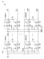
- FIG. 9 shows a memory array 10 according to one embodiment of the present invention.
- the memory array 10 includes N bit lines BL 1 to BLN, M word lines WL 1 to WLM, N operation control lines OL 1 to OLN, M erase control lines EL 1 to ELM, M source lines SL 1 to SLM, and M rows of memory cells 100 ( 1 , 1 ) to 100 (N, 1 ), . . . and 100 ( 1 ,M) to (N,M).
- M and N are positive integers greater than 1.
- Each of the memory cells 100 ( 1 , 1 ) to 100 (N, 1 ), . . . , and 100 ( 1 ,M) to (N,M) can have the same structure as the memory cell 100 as shown in FIG. 1 . Also, in FIG. 9 , memory cells in the same row can be coupled to the same word line, the same source line, and the same erase control line while memory cells in the same column can be coupled to the same bit line, and the same operation control line.
- memory cells 100 ( 1 , 1 ) and 100 (N, 1 ) are disposed in the same row.
- the memory cells 100 ( 1 , 1 ) and 100 (N, 1 ) are coupled to the same word line WL 1 , the same source line SL 1 , and the same erase control line EL 1 .
- the memory cell 100 ( 1 , 1 ) is coupled to the bit line BL 1 and the operation control line OL 1 while the memory cell 100 (N, 1 ) is coupled to the bit line BLN and the operation control line OLN.
- memory cells 100 ( 1 ,M) and 100 (N,M) are disposed in the same row.
- the memory cells 100 ( 1 ,M) and 100 (N,M) are coupled to the same word line WLM, the same source line SLM, and the same erase control line ELM. However, the memory cell 100 ( 1 ,M) is coupled to the bit line BL 1 and the operation control line OL 1 while the memory cell 100 (N,M) is coupled to the bit line BLN and the operation control line OLN.
- memory cells 100 ( 1 , 1 ) and 100 ( 1 ,M) are disposed in the same column.
- the memory cells 100 ( 1 , 1 ) and 100 ( 1 ,M) are coupled to the same bit line BL 1 and the same operation control line OL 1 .
- the memory cell 100 ( 1 , 1 ) is coupled to the word line WL 1 , the source line SL 1 , and the erase control line EL 1 while the memory cell 100 ( 1 ,M) is coupled to the word line WLM, the source line SLM, and the erase control line ELM.
- memory cells 100 (N, 1 ) and 100 (N,M) are disposed in a same column.
- the memory cells 100 (N, 1 ) and 100 (N,M) are coupled to the same bit line BLN and the same operation control line OLN. However, the memory cell 100 (N, 1 ) is coupled to the word line WL 1 , the source line SL 1 , and the erase control line EL 1 while the memory cell 100 (N,M) is coupled to the word line WLM, the source line SLM, and the erase control line ELM.
- FIG. 10 shows voltages of the signals lines coupled to the memory array 10 during a program operation of the memory cell 100 ( 1 , 1 ) according to one embodiment of present invention.
- the source line SL 1 , the bit line BL 1 , and the word line WL 1 are at the first voltage V 1 .
- the operation control line OL 1 is at the second voltage V 2
- the erase control line EL 1 is at the third voltage V 3 .
- the third voltage V 3 is greater than the second voltage V 2
- the second voltage V 2 is greater than the first voltage V 1 .
- the first voltage V 1 can be a ground voltage of the system
- the second voltage V 2 can be 10V
- the third voltage V 3 can be 18V.
- the great voltage gap applied to the second floating gate transistor 140 of the memory cell 100 ( 1 , 1 ) will cause the electron ejection from the common floating gate FG to the body terminal of the second floating gate transistor 140 . Therefore, the electrons reside in the common floating gate FG of the memory cell 100 ( 1 , 1 ) can be ejected to the body terminal of the second floating gate transistor 140 of the memory cell 100 ( 1 , 1 ), and the memory cell 100 ( 1 , 1 ) can be programmed.
- the rest of the memory cells in the memory array 10 are not selected and should not be programmed.
- the memory cell 100 (N, 1 ) is in a same row as the memory cell 100 ( 1 , 1 ).
- the bit line BLN coupled to the unselected memory cell 100 (N, 1 ) is at the first voltage V 1 while the operation control line OLN coupled to the unselected memory cell 100 (N, 1 ) is at the third voltage V 3 .
- the program select transistor 130 of the memory cell 100 (N, 1 ) is turned off. Therefore, the high voltage applied on the second floating gate transistor 140 of the memory cell 100 (N, 1 ) may cause channel depletion and will not induce the electron ejection from the common floating gate FG to the body terminal of the second floating gate transistor 140 . Consequently, the memory cell 100 (N, 1 ) can be inhibited from being programmed during the program operation of the memory cell 100 ( 1 , 1 ).
- the memory cell 100 ( 1 ,M) is in a same column as the memory cell 100 ( 1 , 1 ). Since the memory cell 100 ( 1 ,M) is also coupled to the operation control line OL 1 , which is at the second voltage V 2 during the program operation of the memory cell 100 ( 1 , 1 ), the erase control line ELM coupled to the memory cell 100 ( 1 ,M) should not be too low; otherwise, the program select transistor 130 can be broken down due to the high voltage gap between the operation control line OL 1 and the erase control line ELM. However, the erase control line ELM should not be too high; otherwise, the second floating gate transistor 140 of the memory cell 100 ( 1 ,M) may be programmed unintentionally.
- the word line WLM and the source line SLM coupled to the unselected memory cell 100 ( 1 ,M) are at the first voltage V 1 while the erase control line ELM coupled to the unselected memory cell 100 ( 1 ,M) is at the second voltage V 2 .
- the second voltage V 2 can be 10V while the third voltage V 3 can be 18V. Consequently, the voltage applied on the second floating gate transistor 140 of the memory cell 100 ( 1 ,M) would not be high enough to induce electron ejection. Therefore, the memory cell 100 ( 1 ,M) can be inhibited from being programmed during the program operation of the memory cell 100 ( 1 , 1 ). Also, the program select transistor 130 of the memory cell 100 ( 1 ,M) would not be damaged.
- FIG. 11 shows voltages of the signals lines coupled to the memory array 10 during an erase operation of the memory cell 100 ( 1 , 1 ) according to one embodiment of present invention.
- the source line SL 1 and the word line WL 1 are at a third voltage V 3
- the bit line BL 1 is at the second voltage V 2
- the operation control line OL 1 is at the first voltage V 1 or the second voltage V 2
- the erase control line EL 1 is at the first voltage V 1 . Therefore, the great voltage gap applied to the second floating gate transistor 140 of the memory cell 100 ( 1 , 1 ) will cause the F-N tunneling so the memory cell 100 ( 1 , 1 ) can be erased.
- the unselected memory cells in the memory array 10 should not be erased.
- the memory array 10 is erased row by row. For example, in FIG. 11 , when the memory cell 100 ( 1 , 1 ) is erased, the memory cells disposed in the same row as the memory cell 100 ( 1 , 1 ), such as the memory cell (N, 1 ), would be erased simultaneously. However, memory cells disposed in rows different from the memory cell 100 ( 1 , 1 ) should not be erased.
- the memory cell 100 ( 1 ,M) is disposed in a different row from the memory cell 100 ( 1 , 1 ). Since the memory cell 100 ( 1 ,M) is also coupled to the bit line BL 1 , which is at the second voltage V 2 , the voltage of the source line SLM coupled to the memory cell 100 ( 1 ,M) should not be too low; otherwise, the read select transistor 110 of the memory cell 100 ( 1 ,M) may be damaged. Also, the voltage of the source line SLM should not be too high, otherwise, the memory cell 100 ( 1 ,M) may be erased unintentionally.
- the word line WLM coupled to the unselected memory cell 100 ( 1 ,M) is at the third voltage V 3
- the source line SLM coupled to the unselected memory cell 100 ( 1 ,M) is at the second voltage V 2
- the erase control line ELM coupled to the unselected memory cell 100 ( 1 ,M) is at the first voltage V 1 .
- the second voltage V 2 can be 10V while the third voltage V 3 can be 18V. Consequently, the voltage applied on the first floating gate transistor 120 of the memory cell 100 ( 1 ,M) would not be high enough to induce F-N tunneling. Therefore, the memory cell 100 ( 1 ,M) can be inhibited from being erased during the erase operation of the memory cell 100 ( 1 , 1 ). Also, the read select transistor 110 of the memory cell 100 ( 1 ,M) would not be damaged.
- FIG. 12 shows voltages of the signals lines coupled to the memory array 10 during a read operation of the memory cell 100 ( 1 , 1 ) according to one embodiment of present invention.
- the source line SL 1 is at the fourth voltage V 4
- the bit line BL 1 is at the fifth voltage V 5
- the word line WL 1 , the operation control line OL 1 , the erase control line EL 1 are at the first voltage V 1 .
- the read select transistor 110 of the memory cell 100 ( 1 , 1 ) can be turned on during the read operation of the memory cell 100 ( 1 , 1 ).
- the fourth voltage V 4 can be 5V
- the fifth voltage V 5 can be 3.8V
- the first voltage V 1 can be the ground voltage or 0V. Therefore, the read current is detected according to the status of the common floating gate FG of the memory cell 100 ( 1 , 1 ).
- the unselected memory cells in the memory array 10 should not be read.
- the memory cell 100 (N, 1 ) and the memory cell 100 ( 1 ,M) should not be read.
- the memory cell 100 (N, 1 ) is in a same row as the memory cell 100 ( 1 , 1 ).
- the bit line BLN and the operation control line OLN coupled to the unselected memory cell 100 (N, 1 ) is at the first voltage V 1 .
- the read select transistor 110 of the memory cell 100 (N, 1 ) is turned off so that the memory cell 100 (N, 1 ) is not accessed.
- the memory cell 100 ( 1 ,M) is in a different row from the memory cell 100 ( 1 , 1 ).
- the word line WLM coupled to the unselected memory cell 100 ( 1 ,M) is at the fourth voltage V 4 while the source line SLM and erase control line ELM coupled to the unselected memory cell 100 ( 1 ,M) are at the first voltage V 1 .
- the read select transistor 110 of the memory cell 100 ( 1 ,M) can be turned off so that the memory cell 100 ( 1 ,M) is not accessed.
- the memory array 10 since the electron is ejected and injected on the second floating gate transistors 140 of the memory cells 100 ( 1 , 1 ) to 100 (N,M) while the read current can be detected through the read select transistors 110 and the first floating gate transistors 120 of the memory cells 100 ( 1 , 1 ) to 100 (N,M), the defects on the second floating gate transistors 140 of the memory cells 100 ( 1 , 1 ) to 100 (N,M) caused by the program and erase operations will not affect the read current. Therefore, because the write path and the read path of the memory array 10 are separated, the memory array 10 is able to endure more cycles of program and erase operations without deteriorating the reading ability.
- the memory array 10 can adopt the memory cell 200 as shown in FIG. 7 instead of the memory cell 100 .
- the memory array with memory cells 200 can still function normally while having better endurance.
- the common floating gate would be programmed/erased through the second floating gate transistor while being read through the first floating gate transistor and the read transistor. Therefore, the defect on the common floating gate or the second floating gate transistor will not affect the read current detected by the first floating gate transistor and the read transistor. Consequently, the memory cell and the memory array of the present invention are able to endure more cycles of program and erase operations without deteriorating the reading ability.
Landscapes
- Engineering & Computer Science (AREA)
- Microelectronics & Electronic Packaging (AREA)
- Power Engineering (AREA)
- Physics & Mathematics (AREA)
- Condensed Matter Physics & Semiconductors (AREA)
- General Physics & Mathematics (AREA)
- Computer Hardware Design (AREA)
- Ceramic Engineering (AREA)
- General Engineering & Computer Science (AREA)
- Geometry (AREA)
- Non-Volatile Memory (AREA)
- Read Only Memory (AREA)
- Semiconductor Memories (AREA)
- Logic Circuits (AREA)
- Electronic Switches (AREA)
- Control Of Indicators Other Than Cathode Ray Tubes (AREA)
Abstract
A memory cell includes a read transistor, a first floating gate transistor, a program transistor, a second floating gate transistor, and a common floating gate. The common floating gate is coupled to the second floating gate transistor and the first floating gate transistor. The memory cell is programmed and erased through the common floating gate on the second floating gate transistor, and is read through the first floating gate transistor and the read transistor.
Description
This non-provisional application claims priority of U.S. provisional application No. 62/280,683, filed on Jan. 19, 2016, included herein by reference in its entirety.
1. Field of the Invention
This invention is related to a memory cell, especially to a memory cell with high endurance for multiple program operations.
2. Description of the Prior Art
Non-volatile memory (NVM) is a type of memory that retains information it stores even when no power is supplied to memory blocks thereof.
Due to the wide range of applications for various uses, there is a growing need for a nonvolatile memory to be embedded in the same chip with the main circuit, especially for personal electronic devices having strict requirements for circuit area.
According to the programming times limit, non-volatile memory devices are divided into multi-time programmable (MTP) memory and one-time programmable (OTP) memory. A MTP nonvolatile memory cell of prior art includes one floating gate transistor for retaining data, and one or two select transistors for enabling the floating gate transistor to perform corresponding operations. The floating gate is controlled by two different coupling elements, one for program operations and one for erase operations.
Since the electrons are ejected or injected through the floating gate during the program operations and the erase operations, the floating gate is damaged as the number of operations grows. The defect on the floating gate will deteriorate the memory cell and make it difficult to identify the read current generated by the memory cell.
One embodiment of the present invention discloses a memory cell. The memory includes a read transistor, a first floating gate transistor, a program transistor, a second floating gate transistor, and a common floating gate.
The read select transistor has a first terminal coupled to a bit line, a second terminal, a control terminal coupled to a word line, and a body terminal coupled to a source line. The first floating gate transistor has a first terminal coupled to the second terminal of the read transistor, a second terminal coupled to the source line, and a body terminal coupled to the source line. The program select transistor has a first terminal coupled to an erase control line, a second terminal, a control terminal coupled to an operation control line, and a body terminal coupled to the erase control line. The second floating gate transistor has a first terminal coupled to the second terminal of the program transistor, a second terminal, and a body terminal coupled to the erase control line. The common floating gate is coupled to the first floating gate transistor and the second floating gate transistor. The read transistor, the first floating gate transistor, the program transistor, and the second floating gate transistor are formed by metal-oxide-semiconductors.
Another embodiment of the present invention discloses a memory array. The memory array includes a plurality of bit lines, a plurality of word lines, a plurality of operation control lines, a plurality of erase control lines, a plurality of source lines, and a plurality of rows of memory cells.
Each of memory cells includes a read transistor, a first floating gate transistor, a program transistor, a second floating gate transistor, and a common floating gate. The read select transistor has a first terminal coupled to a bit line of the plurality of bit lines, a second terminal, a control terminal coupled to a word line of the plurality of word lines, and a body terminal coupled to a source line of the plurality of source lines. The first floating gate transistor has a first terminal coupled to the second terminal of the read transistor, a second terminal coupled to the source line, and a body terminal coupled to the source line. The program select transistor has a first terminal coupled to an erase control line of the plurality of erase control lines, a second terminal, a control terminal coupled to an operation control line of the plurality of operation control lines, and a body terminal coupled to the erase control line. The second floating gate transistor has a first terminal coupled to the second terminal of the program transistor, a second terminal, and a body terminal coupled to the erase control line. The common floating gate is coupled to the first floating gate transistor and the second floating gate transistor.
Memory cells in a same row are coupled to a same word line, a same source line, and a same erase control line. Memory cells in a same column are coupled to a same bit line, and a same operation control line.
These and other objectives of the present invention will no doubt become obvious to those of ordinary skill in the art after reading the following detailed description of the preferred embodiment that is illustrated in the various figures and drawings.
The read select transistor 110 has a first terminal, a second terminal, a control terminal and a body terminal. The first terminal of the read select transistor 110 is coupled to a bit line BL, the control terminal of the read select transistor 110 is coupled to a word line WL, and the body terminal of the read select transistor 110 is coupled to a source line SL.
The first floating gate transistor 120 has a first terminal, a second terminal, a control terminal and a body terminal. The first terminal of the first floating gate transistor 120 is coupled to the second terminal of the read select transistor 110, the second terminal of the first floating gate transistor 120 is coupled to the source line SL, and the body terminal of the first floating gate transistor 120 is coupled to the source line SL.
The program select transistor 130 has a first terminal, a second terminal, a control terminal and a body terminal. The first terminal of the program select transistor 130 is coupled to an erase control line EL, the control terminal of the program select transistor 130 is coupled to an operation control line OL, and the body terminal of the program select transistor 130 is coupled to the erase control line EL.
The second floating gate transistor 140 has a first terminal, a second terminal, a control terminal and a body terminal. The first terminal of the second floating gate transistor 140 is coupled to the second terminal of the program select transistor 130, the second terminal of the second floating gate transistor 140 is floating, and the body terminal of the second floating gate transistor 140 is coupled to the erase control line EL. Also, the common floating gate FG is coupled to the first floating gate transistor 120 and the second floating gate transistor 140.
In FIGS. 2 and 3 , the read select transistor 110, the first floating gate transistor 120, the program select transistor 130, and the second floating gate transistor 140 are formed by P-type metal-oxide-semiconductors (PMOS). Also, the read select transistor 110 and the first floating gate transistor 120 can be formed in an oxide diffusion region OD1 of a first N-well NW1 while the program select transistor 130 and the second floating gate transistor 140 can be formed in an oxide diffusion region OD2 of a second N-well NW2. In this embodiment, the first terminals and the second terminals of the read select transistor 110 and the first floating gate transistor 120 can be the P-type doped regions P+ disposed in the oxide diffusion region OD1 in the first N-well NW1, and the body terminals of the read select transistor 110 and the first floating gate transistor 120 can be the rest parts of the oxide diffusion region OD1. In some embodiments, the oxide diffusion region OD1 can be defined by the shallow trench isolation layer STI as shown in FIG. 3 .
Similarly, the first terminals and the second terminals of the program select transistor 130 and the second floating gate transistor 140 can be the P-type doped regions P+ disposed in the oxide diffusion region OD2 in the second N-well NW2, and the body terminals of the program select transistor 130 and the second floating gate transistor 140 can be the rest parts of the oxide diffusion region OD2. The two N-wells NW1 and NW2 can be isolated by a P-well PW on a substrate P-sub.
In FIG. 3 , the body terminal of the program select transistor 130 can be coupled to the erase control line EL through a contact 132, and the contact 132 can be formed on an N-type heavily doped region N+ in the oxide diffusion region OD2 in the N-well NW2. In FIGS. 2 and 3 , the N-type heavily doped region N+ is disposed next to the program select transistor 130. However, in other embodiments, the N-type heavily doped region N+ can be disposed in other places in the oxide diffusion region OD2 in the N-well NW2. Since the second floating gate transistor 140 and the program select transistor 130 are disposed in the same N-well NW2, the body terminal of the second floating gate transistor 140 will be coupled to the erase control line EL as well.
Similarly, the read select transistor 110 and the first floating gate transistor 120 may have the similar structure of as the program select transistor 130 and the second floating gate transistor 140 shown in FIG. 3 . Since the first floating gate transistor 120 and the read select transistor 110 are disposed in the oxide diffusion region OD1 of the same N-well NW1, the body terminals of the read select transistor 110 and the first floating gate transistor 120 can be coupled to the source line SL through a contact on the N-type heavily doped region N+ in the oxide diffusion region OD1 of the N-well NW1.
The common floating gate FG can be a layer of polysilicon formed above the first floating gate transistor 120 and second floating gate transistor 140. Therefore, the voltage of the common floating gate FG can be controlled by the voltage of the body terminal of the first floating gate transistor 120 and the voltage of the body terminal of the second floating gate transistor 140.
Furthermore, an overlap area A1 can be defined by an area on the oxide diffusion region OD1 overlapping the common floating gate FG while an overlap area A2 can be defined by an area on the oxide diffusion region OD2 overlapping the common floating fate FG as shown in FIG. 2 . In the present embodiment, the overlap area A1 is greater than an overlap area A2. Therefore, the voltage of the common floating gate FG would be dominated by the voltage of the body terminal of the first floating gate transistor 120. In some embodiments, to ensure the domination of the first floating gate transistor 120, the overlap area A1 can be nine times greater than the overlap area A2.
In FIG. 4 , during the program operation of the memory cell 100, the source line SL, the bit line BL, and the word line WL are at a first voltage V1. Also, the operation control line OL is at a second voltage V2, and the erase control line EL is at a third voltage V3. The third voltage V3 is greater than the second voltage V2, and the second voltage V2 is greater than the first voltage V1. In some embodiments, the first voltage V1 can be a ground voltage of the system, the second voltage V2 can be 10V, and the third voltage V3 can be 18V.
Therefore, during the program operation of the memory cell 100, the common floating gate FG will be coupled to the first voltage V1 through the first floating gate transistor 120. In this case, since the body terminal of the second floating gate transistor 140 is at the third voltage V3, the great voltage gap applied to the second floating gate transistor 140 will induce the electron ejection. Therefore, the electrons reside in the common floating gate FG will be ejected to the body terminal of the second floating gate transistor 140. Meanwhile, the program select transistor 130 is turned on to ensure that the second floating gate transistor 140 will not enter the depletion mode. Consequently, the second floating gate transistor 140 can be programmed accordingly.
During the erase operation of the memory cell 100, the source line SL and the word line WL are at a third voltage V3, the bit line BL is at the second voltage V2, the operation control line OL is at the first voltage V1 or the second voltage V2, and the erase control line EL is at the first voltage V1.
That is, during the erase operation of the memory cell 100, the body terminal of the second floating gate transistor 140 is at the low voltage of first voltage V1 while the common floating gate FG is coupled to the high voltage of the third voltage V3 through the first floating gate transistor 120. Therefore, the great voltage gap applied to the second floating gate transistor 140 will induce the electron tunneling so that the electrons of the body terminal of the second floating gate transistor 140 will be injected to the common floating gate FG.
During the read operation of the memory cell 100, the source line SL is at a fourth voltage V4, the bit line BL is at a fifth voltage V5, and the word line WL, the operation control line OL, the erase control line EL are at the first voltage V1. The second voltage V2 is greater than the fourth voltage V4, the fourth voltage V4 is greater than the fifth voltage V5, and the fifth V5 voltage is greater than the first voltage V1. For example, the first voltage V1 can be a ground voltage of the system, the second voltage V2 can be 10V, the third voltage V3 can be 18V, the fourth voltage can be 5V, and the fifth voltage can be 3.8V.
That is, during the read operation of the memory cell 100, the read select transistor 110 is turned on while the program select transistor 130 is turned off. Also, the first floating gate transistor 120 and the second floating gate transistor 140 are kept in their previous status. Therefore, a read current is detected through the read select transistor 110 according to the status of the common floating gate FG. For example, if the memory cell 100 is programmed, there would be no electrons stored in the common floating gate FG. In this case, there would be no read current, or only tiny read current. On the contrary, if the memory cell 100 has not been programmed previously, or was programmed previously but has been erased afterwards, then an identifiable read current would be detected. Therefore, by judging the intensity of the read current, the information stored in the memory cell 100 can be identified.
Furthermore, since the electron is ejected or injected on the second floating gate transistor 140 while the read current is flowed through the read select transistor 110 and the first floating gate transistor 120, the defect on the second floating gate transistor 140 caused by the program and erase operations will not affect the generation of the read current. Therefore, because the write path and the read path of the memory cell 100 are separated, the memory cell 100 is able to endure more cycles of program and erase operations without deteriorating the reading ability.
Although the memory cell 100 shown in FIGS. 1 to 6 are formed by PMOS, in some embodiments, the read transistor, the first floating gate transistor, the program transistor, and the second floating gate transistor can be formed by N-type metal-oxide-semiconductors (NMOS).
That is, the body terminals of the read select transistor 210, the first floating gate transistor 220, the program select transistor 230, and the second floating gate transistor 240 are formed by P-type doped wells. In this embodiment, the first P-well PW1 and the second P-well PW2 are disposed in a deep N-well DNW, so that the high voltage applied to the body terminals of the read select transistor 210, the first floating gate transistor 220, the program select transistor 230, and the second floating gate transistor 240 will not cause leakage current.
Each of the memory cells 100(1,1) to 100(N, 1), . . . , and 100(1,M) to (N,M) can have the same structure as the memory cell 100 as shown in FIG. 1 . Also, in FIG. 9 , memory cells in the same row can be coupled to the same word line, the same source line, and the same erase control line while memory cells in the same column can be coupled to the same bit line, and the same operation control line.
For example, memory cells 100(1,1) and 100(N,1) are disposed in the same row. The memory cells 100(1,1) and 100(N,1) are coupled to the same word line WL1, the same source line SL1, and the same erase control line EL1. However, the memory cell 100(1,1) is coupled to the bit line BL1 and the operation control line OL1 while the memory cell 100(N,1) is coupled to the bit line BLN and the operation control line OLN. Similarly, memory cells 100(1,M) and 100(N,M) are disposed in the same row. The memory cells 100(1,M) and 100(N,M) are coupled to the same word line WLM, the same source line SLM, and the same erase control line ELM. However, the memory cell 100(1,M) is coupled to the bit line BL1 and the operation control line OL1 while the memory cell 100(N,M) is coupled to the bit line BLN and the operation control line OLN.
Also, memory cells 100(1,1) and 100(1,M) are disposed in the same column. The memory cells 100(1,1) and 100(1,M) are coupled to the same bit line BL1 and the same operation control line OL1. However, the memory cell 100(1,1) is coupled to the word line WL1, the source line SL1, and the erase control line EL1 while the memory cell 100(1,M) is coupled to the word line WLM, the source line SLM, and the erase control line ELM. Similarly, memory cells 100(N,1) and 100(N,M) are disposed in a same column. The memory cells 100(N,1) and 100(N,M) are coupled to the same bit line BLN and the same operation control line OLN. However, the memory cell 100(N,1) is coupled to the word line WL1, the source line SL1, and the erase control line EL1 while the memory cell 100(N,M) is coupled to the word line WLM, the source line SLM, and the erase control line ELM.
In FIG. 10 , during the program operation of the memory cell 100(1,1), the source line SL1, the bit line BL1, and the word line WL1 are at the first voltage V1. Also, the operation control line OL1 is at the second voltage V2, and the erase control line EL1 is at the third voltage V3. The third voltage V3 is greater than the second voltage V2, and the second voltage V2 is greater than the first voltage V1. In some embodiments, the first voltage V1 can be a ground voltage of the system, the second voltage V2 can be 10V, and the third voltage V3 can be 18V.
In this case, the great voltage gap applied to the second floating gate transistor 140 of the memory cell 100(1,1) will cause the electron ejection from the common floating gate FG to the body terminal of the second floating gate transistor 140. Therefore, the electrons reside in the common floating gate FG of the memory cell 100(1,1) can be ejected to the body terminal of the second floating gate transistor 140 of the memory cell 100(1,1), and the memory cell 100(1,1) can be programmed.
However, during the program operation of the memory cell 100(1,1), the rest of the memory cells in the memory array 10 are not selected and should not be programmed. For example, the memory cell 100(N,1) and the memory cell 100(1,M).
The memory cell 100(N,1) is in a same row as the memory cell 100(1,1). In FIG. 10 , during the program operation of the memory cell 100(1,1), the bit line BLN coupled to the unselected memory cell 100(N,1) is at the first voltage V1 while the operation control line OLN coupled to the unselected memory cell 100(N,1) is at the third voltage V3.
That is, during the program operation of the memory cell 100(1,1), the program select transistor 130 of the memory cell 100(N,1) is turned off. Therefore, the high voltage applied on the second floating gate transistor 140 of the memory cell 100(N,1) may cause channel depletion and will not induce the electron ejection from the common floating gate FG to the body terminal of the second floating gate transistor 140. Consequently, the memory cell 100(N,1) can be inhibited from being programmed during the program operation of the memory cell 100(1,1).
In addition, the memory cell 100(1,M) is in a same column as the memory cell 100(1,1). Since the memory cell 100(1,M) is also coupled to the operation control line OL1, which is at the second voltage V2 during the program operation of the memory cell 100(1,1), the erase control line ELM coupled to the memory cell 100(1,M) should not be too low; otherwise, the program select transistor 130 can be broken down due to the high voltage gap between the operation control line OL1 and the erase control line ELM. However, the erase control line ELM should not be too high; otherwise, the second floating gate transistor 140 of the memory cell 100(1,M) may be programmed unintentionally.
Therefore, in FIG. 10 , during the program operation of the memory cell 100(1,1), the word line WLM and the source line SLM coupled to the unselected memory cell 100(1,M) are at the first voltage V1 while the erase control line ELM coupled to the unselected memory cell 100(1,M) is at the second voltage V2. In this case, for keeping an acceptable voltage gap on the program select transistor 130, the second voltage V2 can be 10V while the third voltage V3 can be 18V. Consequently, the voltage applied on the second floating gate transistor 140 of the memory cell 100(1,M) would not be high enough to induce electron ejection. Therefore, the memory cell 100(1,M) can be inhibited from being programmed during the program operation of the memory cell 100(1,1). Also, the program select transistor 130 of the memory cell 100(1,M) would not be damaged.
During the erase operation of the memory cell 100(1,1), the source line SL1 and the word line WL1 are at a third voltage V3, the bit line BL1 is at the second voltage V2, the operation control line OL1 is at the first voltage V1 or the second voltage V2, and the erase control line EL1 is at the first voltage V1. Therefore, the great voltage gap applied to the second floating gate transistor 140 of the memory cell 100(1,1) will cause the F-N tunneling so the memory cell 100(1,1) can be erased.
However, during the erase operation of the memory cell 100(1,1), the unselected memory cells in the memory array 10 should not be erased. In some embodiments of the present invention, the memory array 10 is erased row by row. For example, in FIG. 11 , when the memory cell 100(1,1) is erased, the memory cells disposed in the same row as the memory cell 100(1,1), such as the memory cell (N,1), would be erased simultaneously. However, memory cells disposed in rows different from the memory cell 100(1,1) should not be erased.
For example, the memory cell 100(1,M) is disposed in a different row from the memory cell 100(1,1). Since the memory cell 100(1,M) is also coupled to the bit line BL1, which is at the second voltage V2, the voltage of the source line SLM coupled to the memory cell 100(1,M) should not be too low; otherwise, the read select transistor 110 of the memory cell 100(1,M) may be damaged. Also, the voltage of the source line SLM should not be too high, otherwise, the memory cell 100(1,M) may be erased unintentionally.
Therefore, in FIG. 11 , during the erase operation of the memory cell 100(1,1), the word line WLM coupled to the unselected memory cell 100(1,M) is at the third voltage V3, the source line SLM coupled to the unselected memory cell 100(1,M) is at the second voltage V2, and the erase control line ELM coupled to the unselected memory cell 100(1,M) is at the first voltage V1.
In this case, for keeping an acceptable voltage gap on the read select transistor 110, the second voltage V2 can be 10V while the third voltage V3 can be 18V. Consequently, the voltage applied on the first floating gate transistor 120 of the memory cell 100(1,M) would not be high enough to induce F-N tunneling. Therefore, the memory cell 100(1,M) can be inhibited from being erased during the erase operation of the memory cell 100(1,1). Also, the read select transistor 110 of the memory cell 100(1,M) would not be damaged.
During the read operation of the memory cell 100(1,1), the source line SL1 is at the fourth voltage V4, the bit line BL1 is at the fifth voltage V5, and the word line WL1, the operation control line OL1, the erase control line EL1 are at the first voltage V1.
Since the fourth voltage V4 is greater than the fifth voltage V5, and the fifth voltage V5 is greater than the first voltage V1, the read select transistor 110 of the memory cell 100(1,1) can be turned on during the read operation of the memory cell 100(1,1). In some embodiments, the fourth voltage V4 can be 5V, the fifth voltage V5 can be 3.8V, and the first voltage V1 can be the ground voltage or 0V. Therefore, the read current is detected according to the status of the common floating gate FG of the memory cell 100(1,1).
However, during the read operation of the memory cell 100(1,1), the unselected memory cells in the memory array 10 should not be read. For example, the memory cell 100(N,1) and the memory cell 100(1,M) should not be read.
The memory cell 100(N,1) is in a same row as the memory cell 100(1,1). In FIG. 12 , during the read operation of the memory cell 100(1,1) , the bit line BLN and the operation control line OLN coupled to the unselected memory cell 100(N,1) is at the first voltage V1. In this case, the read select transistor 110 of the memory cell 100(N,1) is turned off so that the memory cell 100(N,1) is not accessed.
Also, the memory cell 100(1,M) is in a different row from the memory cell 100(1,1). In FIG. 12 , during the read operation of the memory cell 100(1,1), the word line WLM coupled to the unselected memory cell 100(1,M) is at the fourth voltage V4 while the source line SLM and erase control line ELM coupled to the unselected memory cell 100(1,M) are at the first voltage V1. In this case, the read select transistor 110 of the memory cell 100(1,M) can be turned off so that the memory cell 100(1,M) is not accessed.
In the memory array 10, since the electron is ejected and injected on the second floating gate transistors 140 of the memory cells 100(1,1) to 100(N,M) while the read current can be detected through the read select transistors 110 and the first floating gate transistors 120 of the memory cells 100(1,1) to 100(N,M), the defects on the second floating gate transistors 140 of the memory cells 100(1,1) to 100(N,M) caused by the program and erase operations will not affect the read current. Therefore, because the write path and the read path of the memory array 10 are separated, the memory array 10 is able to endure more cycles of program and erase operations without deteriorating the reading ability.
Furthermore, in some embodiments, the memory array 10 can adopt the memory cell 200 as shown in FIG. 7 instead of the memory cell 100. By controlling the signals properly, the memory array with memory cells 200 can still function normally while having better endurance.
In summary, according to the memory cells and the memory arrays provided by the embodiments of the present invention, the common floating gate would be programmed/erased through the second floating gate transistor while being read through the first floating gate transistor and the read transistor. Therefore, the defect on the common floating gate or the second floating gate transistor will not affect the read current detected by the first floating gate transistor and the read transistor. Consequently, the memory cell and the memory array of the present invention are able to endure more cycles of program and erase operations without deteriorating the reading ability.
Those skilled in the art will readily observe that numerous modifications and alterations of the device and method may be made while retaining the teachings of the invention. Accordingly, the above disclosure should be construed as limited only by the metes and bounds of the appended claims.
Claims (23)
1. A memory cell comprising:
a read select transistor having a first terminal coupled to a bit line, a second terminal, a control terminal coupled to a word line, and a body terminal coupled to a source line;
a first floating gate transistor having a first terminal coupled to the second terminal of the read transistor, a second terminal coupled to the source line, and a body terminal coupled to the source line;
a program select transistor having a first terminal coupled to an erase control line, a second terminal, a control terminal coupled to an operation control line, and a body terminal coupled to the erase control line;
a second floating gate transistor having a first terminal coupled to the second terminal of the program transistor, a second terminal, and a body terminal coupled to the erase control line; and
a common floating gate coupled to the first floating gate transistor and the second floating gate transistor.
2. The memory cell of claim 1 , wherein a first overlap area on a first oxide diffusion region overlapping the common floating gate is greater than a second overlap area on a second oxide diffusion region overlapping the common floating gate.
3. The memory cell of claim 1 , wherein the read transistor, the first floating gate transistor, the program transistor, and the second floating gate transistor are formed by P-type metal-oxide-semiconductors (PMOS).
4. The memory cell of claim 3 , wherein:
the read select transistor and the first floating gate transistor are formed in a first N-well; and
the program select transistor and the second floating gate transistor are formed in a second N-well.
5. The memory cell of claim 3 , wherein during a program operation of the memory cell:
the source line is at a first voltage (0V);
the bit line is at the first voltage (0V);
the word line is at the first voltage (0V);
the operation control line is at a second voltage (10V); and
the erase control line is at a third voltage (18V);
wherein the third voltage is greater than the second voltage, and the second voltage is greater than the first voltage.
6. The memory cell of claim 5 , wherein during a read operation of the memory cell:
the source line is at a fourth voltage (5V);
the bit line is at a fifth voltage (3.8V);
the word line is at the first voltage (0V);
the operation control line is at the first voltage (0V); and
the erase control line is at the first voltage (0V);
wherein the second voltage is greater than the fourth voltage, the fourth voltage is greater than the fifth voltage, and the fifth voltage is greater than the first voltage.
7. The memory cell of claim 3 , wherein during an erase operation of the memory cell:
the source line is at a third voltage (18V);
the bit line is at a second voltage (10V);
the word line is at the third voltage (18V);
the operation control line is at a first voltage or the second voltage (10V); and
the erase control line is at the first voltage (0V);
wherein the third voltage is greater than the second voltage, and the second voltage is greater than the first voltage.
8. The memory cell of claim 1 , wherein the read transistor, the first floating gate transistor, the program transistor, and the second floating gate transistor are formed by N-type metal-oxide-semiconductors (NMOS).
9. The memory cell of claim 8 , wherein:
the read select transistor and the first floating gate transistor are formed in a first P-well;
the program select transistor and the second floating gate transistor are formed in a second P-well; and
the first P-well and the second P-well are disposed in a deep N-well.
10. A memory array comprising:
a plurality of bit lines;
a plurality of word lines;
a plurality of operation control lines;
a plurality of erase control lines;
a plurality of source lines; and
a plurality of rows of memory cells, each comprising:
a read select transistor having a first terminal coupled to a bit line of the plurality of bit lines, a second terminal, a control terminal coupled to a word line of the plurality of word lines, and a body terminal coupled to a source line of the plurality of source lines;
a first floating gate transistor having a first terminal coupled to the second terminal of the read transistor, a second terminal coupled to the source line, and a body terminal coupled to the source line;
a program select transistor having a first terminal coupled to an erase control line of the plurality of erase control lines, a second terminal, a control terminal coupled to an operation control line of the plurality of operation control lines, and a body terminal coupled to the erase control line;
a second floating gate transistor having a first terminal coupled to the second terminal of the program transistor, a second terminal, and a body terminal coupled to the erase control line; and
a common floating gate coupled to the first floating gate transistor and the second floating gate transistor;
wherein:
memory cells in a same row are coupled to a same word line, a same source line, and a same erase control line; and
memory cells in a same column are coupled to a same bit line, and a same operation control line.
11. The memory array of claim 10 , wherein a first overlap area on a first oxide diffusion region overlapping the common floating gate is greater than a second overlap area on a second oxide diffusion region overlapping the common floating gate.
12. The memory array of claim 10 , wherein the read transistor, the first floating gate transistor, the program transistor, and the second floating gate transistor are formed by P-type metal-oxide-semiconductors (PMOS).
13. The memory array of claim 12 , wherein:
the read select transistor and the first floating gate transistor are formed in a first N-well; and
the program select transistor and the second floating gate transistor are formed in a second N-well.
14. The memory array of claim 12 , wherein during a program operation of the memory cell:
the source line is at a first voltage (0V);
the bit line is at the first voltage (0V);
the word line is at the first voltage (0V);
the operation control line is at a second voltage (10V); and
the erase control line is at a third voltage (18V);
wherein the third voltage is greater than the second voltage, and the second voltage is greater than the first voltage.
15. The memory array of claim 14 , wherein during the program operation of the memory cell:
a bit line coupled to an unselected memory cell in a same row as the memory cell is at the first voltage (0V); and
an operation control line coupled to the unselected memory cell is at the third voltage (18V).
16. The memory array of claim 14 , wherein during the program operation of the memory cell:
a word line coupled to an unselected memory cell in a same column as the memory cell is at the first voltage (0V);
a source line coupled to the unselected memory cell is at the first voltage (0V); and
an erase control line coupled to the unselected memory cell is at the second voltage (10V).
17. The memory array of claim 14 , wherein during a read operation of the memory cell:
the source line is at a fourth voltage (5V);
the bit line is at a fifth voltage (3.8V);
the word line is at the first voltage (0V);
the operation control line is at the first voltage (0V); and
the erase control line is at the first voltage (0V);
wherein the second voltage is greater than the fourth voltage, the fourth voltage is greater than the fifth voltage, and the fifth voltage is greater than the first voltage.
18. The memory array of claim 17 , wherein during the read operation of the memory cell:
a bit line coupled to an unselected memory cell in a same row as the memory cell is at the first voltage (0V); and
an operation control line coupled to the unselected memory cell is at the first voltage (0V).
19. The memory array of claim 17 , wherein during the read operation of the memory cell:
a word line coupled to an unselected memory cell in a same column as the memory cell is at the fourth voltage (5V);
a source line coupled to the unselected memory cell is at the first voltage (0V); and
an erase control line coupled to the unselected memory cell is at the first voltage (0V).
20. The memory array of claim 12 , wherein during an erase operation of the memory cell:
the source line is at a third voltage (18V);
the bit line is at a second voltage (10V);
the word line is at the third voltage (18V);
the operation control line is at a first voltage (0V) or the second voltage (10V); and
the erase control line is at the first voltage (0V);
wherein the third voltage is greater than the second voltage, and the second voltage is greater than the first voltage.
21. The memory array of claim 20 , wherein during the erase operation of the memory cell:
a word line coupled to an unselected memory cell in a same column as the memory cell is at the third voltage (18V);
a source line coupled to the unselected memory cell is at the second voltage (10V); and
an erase control line coupled to the unselected memory cell is at the first voltage (0V).
22. The memory array of claim 10 , wherein the read transistor, the first floating gate transistor, the program transistor, and the second floating gate transistor are formed by N-type metal-oxide-semiconductors (NMOS).
23. The memory array of claim 22 , wherein:
the read select transistor and the first floating gate transistor are formed in a first P-well;
the program select transistor and the second floating gate transistor are formed in a second P-well; and
the first P-well and the second P-well are disposed in a deep N-well.
Priority Applications (3)
| Application Number | Priority Date | Filing Date | Title |
|---|---|---|---|
| US15/406,802 US9792993B2 (en) | 2016-01-19 | 2017-01-16 | Memory cell with high endurance for multiple program operations |
| TW106113346A TWI613654B (en) | 2016-01-19 | 2017-04-21 | Memory cell and memory array |
| CN201710290037.6A CN108320772B (en) | 2016-01-19 | 2017-04-27 | Memory cell and memory array |
Applications Claiming Priority (2)
| Application Number | Priority Date | Filing Date | Title |
|---|---|---|---|
| US201662280683P | 2016-01-19 | 2016-01-19 | |
| US15/406,802 US9792993B2 (en) | 2016-01-19 | 2017-01-16 | Memory cell with high endurance for multiple program operations |
Publications (2)
| Publication Number | Publication Date |
|---|---|
| US20170206969A1 US20170206969A1 (en) | 2017-07-20 |
| US9792993B2 true US9792993B2 (en) | 2017-10-17 |
Family
ID=56137184
Family Applications (13)
| Application Number | Title | Priority Date | Filing Date |
|---|---|---|---|
| US15/150,440 Active US9847133B2 (en) | 2016-01-19 | 2016-05-10 | Memory array capable of performing byte erase operation |
| US15/152,047 Active US9520196B1 (en) | 2016-01-19 | 2016-05-11 | Voltage switch circuit |
| US15/252,244 Active US10262746B2 (en) | 2016-01-19 | 2016-08-31 | Nonvolatile memory structure |
| US15/347,158 Active US9786340B2 (en) | 2016-01-19 | 2016-11-09 | Driving circuit for non-volatile memory |
| US15/352,609 Active US9941011B2 (en) | 2016-01-19 | 2016-11-16 | Memory array with one shared deep doped region |
| US15/368,658 Active US9653173B1 (en) | 2016-01-19 | 2016-12-04 | Memory cell with different program and read paths for achieving high endurance |
| US15/381,089 Active US9805776B2 (en) | 2016-01-19 | 2016-12-15 | Memory device, peripheral circuit thereof and single-byte data write method thereof |
| US15/384,323 Active US10038003B2 (en) | 2016-01-19 | 2016-12-20 | Single-poly nonvolatile memory cell structure having an erase device |
| US15/397,043 Active US10121550B2 (en) | 2016-01-19 | 2017-01-03 | Power switch circuit |
| US15/406,802 Active US9792993B2 (en) | 2016-01-19 | 2017-01-16 | Memory cell with high endurance for multiple program operations |
| US15/408,434 Active US9812212B2 (en) | 2016-01-19 | 2017-01-18 | Memory cell with low reading voltages |
| US15/905,802 Active US10255980B2 (en) | 2016-01-19 | 2018-02-26 | Memory array with one shared deep doped region |
| US15/978,363 Active US10096368B2 (en) | 2016-01-19 | 2018-05-14 | Power switch circuit for non-volatile memory |
Family Applications Before (9)
| Application Number | Title | Priority Date | Filing Date |
|---|---|---|---|
| US15/150,440 Active US9847133B2 (en) | 2016-01-19 | 2016-05-10 | Memory array capable of performing byte erase operation |
| US15/152,047 Active US9520196B1 (en) | 2016-01-19 | 2016-05-11 | Voltage switch circuit |
| US15/252,244 Active US10262746B2 (en) | 2016-01-19 | 2016-08-31 | Nonvolatile memory structure |
| US15/347,158 Active US9786340B2 (en) | 2016-01-19 | 2016-11-09 | Driving circuit for non-volatile memory |
| US15/352,609 Active US9941011B2 (en) | 2016-01-19 | 2016-11-16 | Memory array with one shared deep doped region |
| US15/368,658 Active US9653173B1 (en) | 2016-01-19 | 2016-12-04 | Memory cell with different program and read paths for achieving high endurance |
| US15/381,089 Active US9805776B2 (en) | 2016-01-19 | 2016-12-15 | Memory device, peripheral circuit thereof and single-byte data write method thereof |
| US15/384,323 Active US10038003B2 (en) | 2016-01-19 | 2016-12-20 | Single-poly nonvolatile memory cell structure having an erase device |
| US15/397,043 Active US10121550B2 (en) | 2016-01-19 | 2017-01-03 | Power switch circuit |
Family Applications After (3)
| Application Number | Title | Priority Date | Filing Date |
|---|---|---|---|
| US15/408,434 Active US9812212B2 (en) | 2016-01-19 | 2017-01-18 | Memory cell with low reading voltages |
| US15/905,802 Active US10255980B2 (en) | 2016-01-19 | 2018-02-26 | Memory array with one shared deep doped region |
| US15/978,363 Active US10096368B2 (en) | 2016-01-19 | 2018-05-14 | Power switch circuit for non-volatile memory |
Country Status (5)
| Country | Link |
|---|---|
| US (13) | US9847133B2 (en) |
| EP (6) | EP3196883B1 (en) |
| JP (4) | JP6122531B1 (en) |
| CN (10) | CN106981311B (en) |
| TW (11) | TWI578322B (en) |
Families Citing this family (39)
| Publication number | Priority date | Publication date | Assignee | Title |
|---|---|---|---|---|
| US9965267B2 (en) | 2015-11-19 | 2018-05-08 | Raytheon Company | Dynamic interface for firmware updates |
| US9847133B2 (en) * | 2016-01-19 | 2017-12-19 | Ememory Technology Inc. | Memory array capable of performing byte erase operation |
| US9633734B1 (en) * | 2016-07-14 | 2017-04-25 | Ememory Technology Inc. | Driving circuit for non-volatile memory |
| CN107768373B (en) * | 2016-08-15 | 2022-05-10 | 华邦电子股份有限公司 | Memory element and method for manufacturing the same |
| US9882566B1 (en) * | 2017-01-10 | 2018-01-30 | Ememory Technology Inc. | Driving circuit for non-volatile memory |
| TWI652683B (en) * | 2017-10-13 | 2019-03-01 | 力旺電子股份有限公司 | Voltage driver for memory |
| US10332597B2 (en) * | 2017-11-08 | 2019-06-25 | Globalfoundries Singapore Pte. Ltd. | Floating gate OTP/MTP structure and method for producing the same |
| JP7143326B2 (en) | 2017-12-20 | 2022-09-28 | タワー パートナーズ セミコンダクター株式会社 | semiconductor equipment |
| KR102385951B1 (en) * | 2018-02-23 | 2022-04-14 | 에스케이하이닉스 시스템아이씨 주식회사 | One time programable memory capable of increasing program efficiency and method of fabricating the same |
| KR102422839B1 (en) * | 2018-02-23 | 2022-07-19 | 에스케이하이닉스 시스템아이씨 주식회사 | Non-volatile memory device having a lateral coupling structure and single-layer gate |
| US10522202B2 (en) * | 2018-04-23 | 2019-12-31 | Taiwan Semiconductor Manufacturing Co., Ltd. | Memory device and compensation method therein |
| US10964708B2 (en) * | 2018-06-26 | 2021-03-30 | Micron Technology, Inc. | Fuse-array element |
| CN108986866B (en) * | 2018-07-20 | 2020-12-11 | 上海华虹宏力半导体制造有限公司 | Read high voltage transmission circuit |
| TWI659502B (en) * | 2018-08-02 | 2019-05-11 | 旺宏電子股份有限公司 | Non-volatile memory structure |
| CN110828464A (en) * | 2018-08-08 | 2020-02-21 | 旺宏电子股份有限公司 | Non-volatile memory structure |
| DE102019120605B4 (en) | 2018-08-20 | 2022-06-23 | Taiwan Semiconductor Manufacturing Company, Ltd. | MEMORY CIRCUIT AND METHOD OF PRODUCTION THEREOF |
| US11176969B2 (en) | 2018-08-20 | 2021-11-16 | Taiwan Semiconductor Manufacturing Company, Ltd. | Memory circuit including a first program device |
| CN109147851B (en) * | 2018-08-31 | 2020-12-25 | 上海华力微电子有限公司 | Latch circuit |
| KR20200031894A (en) * | 2018-09-17 | 2020-03-25 | 에스케이하이닉스 주식회사 | Memory module and memory system including the same |
| US10797064B2 (en) * | 2018-09-19 | 2020-10-06 | Ememory Technology Inc. | Single-poly non-volatile memory cell and operating method thereof |
| CN109524042B (en) * | 2018-09-21 | 2020-03-17 | 浙江大学 | NAND type storage array based on inversion mode resistance change field effect transistor |
| TWI708253B (en) | 2018-11-16 | 2020-10-21 | 力旺電子股份有限公司 | Nonvolatile memory yield improvement and testing method |
| CN111342541B (en) * | 2018-12-19 | 2021-04-16 | 智原微电子(苏州)有限公司 | Power supply switching circuit |
| KR20200104669A (en) * | 2019-02-27 | 2020-09-04 | 삼성전자주식회사 | Integrated circuit devices |
| US10924112B2 (en) * | 2019-04-11 | 2021-02-16 | Ememory Technology Inc. | Bandgap reference circuit |
| US11508719B2 (en) | 2019-05-13 | 2022-11-22 | Ememory Technology Inc. | Electrostatic discharge circuit |
| CN112086115B (en) * | 2019-06-14 | 2023-03-28 | 力旺电子股份有限公司 | Memory system |
| CN112131037B (en) * | 2019-06-24 | 2023-11-14 | 华邦电子股份有限公司 | memory device |
| JP2021048230A (en) * | 2019-09-18 | 2021-03-25 | キオクシア株式会社 | Semiconductor storage device |
| US11521980B2 (en) * | 2019-11-14 | 2022-12-06 | Ememory Technology Inc. | Read-only memory cell and associated memory cell array |
| US11139006B1 (en) * | 2020-03-12 | 2021-10-05 | Ememory Technology Inc. | Self-biased sense amplification circuit |
| US11217281B2 (en) * | 2020-03-12 | 2022-01-04 | Ememory Technology Inc. | Differential sensing device with wide sensing margin |
| JP6887044B1 (en) * | 2020-05-22 | 2021-06-16 | ウィンボンド エレクトロニクス コーポレーション | Semiconductor storage device and readout method |
| TWI739695B (en) * | 2020-06-14 | 2021-09-11 | 力旺電子股份有限公司 | Level shifter |
| US11373715B1 (en) * | 2021-01-14 | 2022-06-28 | Elite Semiconductor Microelectronics Technology Inc. | Post over-erase correction method with auto-adjusting verification and leakage degree detection |
| TWI819457B (en) * | 2021-02-18 | 2023-10-21 | 力旺電子股份有限公司 | Memory cell array of multi-time programmable non-volatile memory |
| US11854647B2 (en) * | 2021-07-29 | 2023-12-26 | Micron Technology, Inc. | Voltage level shifter transition time reduction |
| US11972800B2 (en) * | 2021-12-16 | 2024-04-30 | Ememory Technology Inc. | Non-volatile memory cell and non-volatile memory cell array |
| US12014783B2 (en) | 2022-01-10 | 2024-06-18 | Ememory Technology Inc. | Driving circuit for non-volatile memory |
Citations (3)
| Publication number | Priority date | Publication date | Assignee | Title |
|---|---|---|---|---|
| US5331590A (en) | 1991-10-15 | 1994-07-19 | Lattice Semiconductor Corporation | Single poly EE cell with separate read/write paths and reduced product term coupling |
| US20060018161A1 (en) * | 2004-07-20 | 2006-01-26 | Hsin-Ming Chen | Single poly non-volatile memory |
| US8139411B1 (en) | 2008-05-22 | 2012-03-20 | Synopsys, Inc. | pFET nonvolatile memory |
Family Cites Families (167)
| Publication number | Priority date | Publication date | Assignee | Title |
|---|---|---|---|---|
| US4617652A (en) | 1979-01-24 | 1986-10-14 | Xicor, Inc. | Integrated high voltage distribution and control systems |
| JP2685966B2 (en) | 1990-06-22 | 1997-12-08 | 株式会社東芝 | Nonvolatile semiconductor memory device |
| JP3180608B2 (en) | 1994-03-28 | 2001-06-25 | 松下電器産業株式会社 | Power supply selection circuit |
| JP3068752B2 (en) | 1994-08-29 | 2000-07-24 | 松下電器産業株式会社 | Semiconductor device |
| US5648669A (en) * | 1995-05-26 | 1997-07-15 | Cypress Semiconductor | High speed flash memory cell structure and method |
| US5742542A (en) * | 1995-07-03 | 1998-04-21 | Advanced Micro Devices, Inc. | Non-volatile memory cells using only positive charge to store data |
| US5640344A (en) * | 1995-07-25 | 1997-06-17 | Btr, Inc. | Programmable non-volatile bidirectional switch for programmable logic |
| US6005806A (en) * | 1996-03-14 | 1999-12-21 | Altera Corporation | Nonvolatile configuration cells and cell arrays |
| JP4659662B2 (en) | 1997-04-28 | 2011-03-30 | ペグレ・セミコンダクターズ・リミテッド・ライアビリティ・カンパニー | Semiconductor device and manufacturing method thereof |
| FR2767219B1 (en) * | 1997-08-08 | 1999-09-17 | Commissariat Energie Atomique | ELECTRICALLY COMPATIBLE PROGRAMMABLE AND ERASABLE NON-VOLATILE MEMORY DEVICE WITH A CMOS / SELF-MANUFACTURING PROCESS |
| JP3037236B2 (en) * | 1997-11-13 | 2000-04-24 | 日本電気アイシーマイコンシステム株式会社 | Level shifter circuit |
| US5959889A (en) * | 1997-12-29 | 1999-09-28 | Cypress Semiconductor Corp. | Counter-bias scheme to reduce charge gain in an electrically erasable cell |
| DE19808525A1 (en) | 1998-02-27 | 1999-09-02 | Siemens Ag | Integrated circuit |
| JP2000021183A (en) | 1998-06-30 | 2000-01-21 | Matsushita Electric Ind Co Ltd | Semiconductor nonvolatile memory |
| US5999451A (en) | 1998-07-13 | 1999-12-07 | Macronix International Co., Ltd. | Byte-wide write scheme for a page flash device |
| JP3344331B2 (en) | 1998-09-30 | 2002-11-11 | 日本電気株式会社 | Nonvolatile semiconductor memory device |
| JP2000276889A (en) | 1999-03-23 | 2000-10-06 | Toshiba Corp | Non-volatile semiconductor memory |
| CN1376313A (en) * | 1999-08-27 | 2002-10-23 | 马克罗尼克斯美国公司 | Non-volatile memory structure for twin-bit storage and methods of making same |
| JP2001068650A (en) * | 1999-08-30 | 2001-03-16 | Hitachi Ltd | Semiconductor integrated circuit device |
| KR100338772B1 (en) * | 2000-03-10 | 2002-05-31 | 윤종용 | Word line driver having divided bias line in non-volatile memory device and method thereof |
| US6370071B1 (en) * | 2000-09-13 | 2002-04-09 | Lattice Semiconductor Corporation | High voltage CMOS switch |
| AU2002339620A1 (en) * | 2001-11-27 | 2003-06-10 | Koninklijke Philips Electronics N.V. | Semiconductor device having a byte-erasable eeprom memory |
| TW536818B (en) | 2002-05-03 | 2003-06-11 | Ememory Technology Inc | Single-poly EEPROM |
| US6621745B1 (en) * | 2002-06-18 | 2003-09-16 | Atmel Corporation | Row decoder circuit for use in programming a memory device |
| US6774704B2 (en) | 2002-10-28 | 2004-08-10 | Tower Semiconductor Ltd. | Control circuit for selecting the greater of two voltage signals |
| US7038947B2 (en) * | 2002-12-19 | 2006-05-02 | Taiwan Semiconductor Manufacturing Co., Ltd. | Two-transistor flash cell for large endurance application |
| CN1224106C (en) * | 2003-03-05 | 2005-10-19 | 力旺电子股份有限公司 | ROM and its manufacture |
| JP2004326864A (en) | 2003-04-22 | 2004-11-18 | Toshiba Corp | Nonvolatile semiconductor memory |
| FR2856185A1 (en) | 2003-06-12 | 2004-12-17 | St Microelectronics Sa | WORD PROGRAMMABLE FLASH MEMORY |
| US6963503B1 (en) | 2003-07-11 | 2005-11-08 | Altera Corporation. | EEPROM with improved circuit performance and reduced cell size |
| JP2005051227A (en) * | 2003-07-17 | 2005-02-24 | Nec Electronics Corp | Semiconductor memory device |
| US7169667B2 (en) * | 2003-07-30 | 2007-01-30 | Promos Technologies Inc. | Nonvolatile memory cell with multiple floating gates formed after the select gate |
| US7081774B2 (en) * | 2003-07-30 | 2006-07-25 | Semiconductor Energy Laboratory Co., Ltd. | Circuit having source follower and semiconductor device having the circuit |
| US7145370B2 (en) | 2003-09-05 | 2006-12-05 | Impinj, Inc. | High-voltage switches in single-well CMOS processes |
| US20050134355A1 (en) | 2003-12-18 | 2005-06-23 | Masato Maede | Level shift circuit |
| US20050205969A1 (en) * | 2004-03-19 | 2005-09-22 | Sharp Laboratories Of America, Inc. | Charge trap non-volatile memory structure for 2 bits per transistor |
| US7580311B2 (en) * | 2004-03-30 | 2009-08-25 | Virage Logic Corporation | Reduced area high voltage switch for NVM |
| US7629640B2 (en) * | 2004-05-03 | 2009-12-08 | The Regents Of The University Of California | Two bit/four bit SONOS flash memory cell |
| EP1610343B1 (en) * | 2004-06-24 | 2007-12-19 | STMicroelectronics S.r.l. | An improved page buffer for a programmable memory device |
| US6992927B1 (en) | 2004-07-08 | 2006-01-31 | National Semiconductor Corporation | Nonvolatile memory cell |
| KR100633332B1 (en) * | 2004-11-09 | 2006-10-11 | 주식회사 하이닉스반도체 | Negative voltage generator circuit |
| KR100642631B1 (en) * | 2004-12-06 | 2006-11-10 | 삼성전자주식회사 | Voltage generator and semiconductor memory device comprising the same |
| US7369438B2 (en) | 2004-12-28 | 2008-05-06 | Aplus Flash Technology, Inc. | Combo memory design and technology for multiple-function java card, sim-card, bio-passport and bio-id card applications |
| US7193265B2 (en) | 2005-03-16 | 2007-03-20 | United Microelectronics Corp. | Single-poly EEPROM |
| US7263001B2 (en) | 2005-03-17 | 2007-08-28 | Impinj, Inc. | Compact non-volatile memory cell and array system |
| US7288964B2 (en) | 2005-08-12 | 2007-10-30 | Ememory Technology Inc. | Voltage selective circuit of power source |
| JP4800109B2 (en) | 2005-09-13 | 2011-10-26 | ルネサスエレクトロニクス株式会社 | Semiconductor device |
| JP2007149997A (en) | 2005-11-29 | 2007-06-14 | Nec Electronics Corp | Nonvolatile memory cell and eeprom |
| US7382658B2 (en) | 2006-01-26 | 2008-06-03 | Mosys, Inc. | Non-volatile memory embedded in a conventional logic process and methods for operating same |
| US7391647B2 (en) * | 2006-04-11 | 2008-06-24 | Mosys, Inc. | Non-volatile memory in CMOS logic process and method of operation thereof |
| US20070247915A1 (en) * | 2006-04-21 | 2007-10-25 | Intersil Americas Inc. | Multiple time programmable (MTP) PMOS floating gate-based non-volatile memory device for a general-purpose CMOS technology with thick gate oxide |
| US7773416B2 (en) * | 2006-05-26 | 2010-08-10 | Macronix International Co., Ltd. | Single poly, multi-bit non-volatile memory device and methods for operating the same |
| JP4901325B2 (en) | 2006-06-22 | 2012-03-21 | ルネサスエレクトロニクス株式会社 | Semiconductor device |
| US20070296034A1 (en) | 2006-06-26 | 2007-12-27 | Hsin-Ming Chen | Silicon-on-insulator (soi) memory device |
| TWI373127B (en) * | 2006-06-26 | 2012-09-21 | Ememory Technology Inc | Nonvolatile single-poly memory device |
| US7768059B2 (en) | 2006-06-26 | 2010-08-03 | Ememory Technology Inc. | Nonvolatile single-poly memory device |
| JP5005970B2 (en) | 2006-06-27 | 2012-08-22 | 株式会社リコー | Voltage control circuit and semiconductor integrated circuit having voltage control circuit |
| CN100508169C (en) * | 2006-08-02 | 2009-07-01 | 联华电子股份有限公司 | Method for manufacturing single level polysilicon electric removal and programmable read only memory cell |
| US7586792B1 (en) * | 2006-08-24 | 2009-09-08 | National Semiconductor Corporation | System and method for providing drain avalanche hot carrier programming for non-volatile memory applications |
| KR100805839B1 (en) * | 2006-08-29 | 2008-02-21 | 삼성전자주식회사 | Flash memory device sharing a high voltage generator |
| US7483310B1 (en) * | 2006-11-02 | 2009-01-27 | National Semiconductor Corporation | System and method for providing high endurance low cost CMOS compatible EEPROM devices |
| KR100781041B1 (en) * | 2006-11-06 | 2007-11-30 | 주식회사 하이닉스반도체 | Flash memory device and method for controlling erase operation of the same |
| JP4863844B2 (en) * | 2006-11-08 | 2012-01-25 | セイコーインスツル株式会社 | Voltage switching circuit |
| US8378407B2 (en) | 2006-12-07 | 2013-02-19 | Tower Semiconductor, Ltd. | Floating gate inverter type memory cell and array |
| US7755941B2 (en) * | 2007-02-23 | 2010-07-13 | Panasonic Corporation | Nonvolatile semiconductor memory device |
| US7436710B2 (en) | 2007-03-12 | 2008-10-14 | Maxim Integrated Products, Inc. | EEPROM memory device with cell having NMOS in a P pocket as a control gate, PMOS program/erase transistor, and PMOS access transistor in a common well |
| WO2008114342A1 (en) * | 2007-03-16 | 2008-09-25 | Fujitsu Microelectronics Limited | Power switch circuit and semiconductor integrated circuit device |
| US7663916B2 (en) | 2007-04-16 | 2010-02-16 | Taiwan Semicondcutor Manufacturing Company, Ltd. | Logic compatible arrays and operations |
| US7903465B2 (en) * | 2007-04-24 | 2011-03-08 | Intersil Americas Inc. | Memory array of floating gate-based non-volatile memory cells |
| JP4455621B2 (en) * | 2007-07-17 | 2010-04-21 | 株式会社東芝 | Aging device |
| US8369155B2 (en) * | 2007-08-08 | 2013-02-05 | Hynix Semiconductor Inc. | Operating method in a non-volatile memory device |
| JP2009049182A (en) | 2007-08-20 | 2009-03-05 | Toyota Motor Corp | Nonvolatile semiconductor storage element |
| US7700993B2 (en) * | 2007-11-05 | 2010-04-20 | International Business Machines Corporation | CMOS EPROM and EEPROM devices and programmable CMOS inverters |
| KR101286241B1 (en) | 2007-11-26 | 2013-07-15 | 삼성전자주식회사 | Maximum voltage source selector |
| US7968926B2 (en) | 2007-12-19 | 2011-06-28 | Taiwan Semiconductor Manufacturing Company, Ltd. | Logic non-volatile memory cell with improved data retention ability |
| US8576628B2 (en) * | 2008-01-18 | 2013-11-05 | Sharp Kabushiki Kaisha | Nonvolatile random access memory |
| US7639536B2 (en) | 2008-03-07 | 2009-12-29 | United Microelectronics Corp. | Storage unit of single-conductor non-volatile memory cell and method of erasing the same |
| US7800426B2 (en) | 2008-03-27 | 2010-09-21 | Taiwan Semiconductor Manufacturing Co., Ltd. | Two voltage input level shifter with switches for core power off application |
| JP5266443B2 (en) * | 2008-04-18 | 2013-08-21 | インターチップ株式会社 | Nonvolatile memory cell and non-volatile memory cell built-in data latch |
| US8344443B2 (en) | 2008-04-25 | 2013-01-01 | Freescale Semiconductor, Inc. | Single poly NVM devices and arrays |
| US8218377B2 (en) * | 2008-05-19 | 2012-07-10 | Stmicroelectronics Pvt. Ltd. | Fail-safe high speed level shifter for wide supply voltage range |
| US8295087B2 (en) * | 2008-06-16 | 2012-10-23 | Aplus Flash Technology, Inc. | Row-decoder and select gate decoder structures suitable for flashed-based EEPROM operating below +/− 10v BVDS |
| KR101462487B1 (en) * | 2008-07-07 | 2014-11-18 | 삼성전자주식회사 | Flash memory device and programming method thereof |
| US7983081B2 (en) | 2008-12-14 | 2011-07-19 | Chip.Memory Technology, Inc. | Non-volatile memory apparatus and method with deep N-well |
| US8189390B2 (en) * | 2009-03-05 | 2012-05-29 | Mosaid Technologies Incorporated | NAND flash architecture with multi-level row decoding |
| US8319528B2 (en) * | 2009-03-26 | 2012-11-27 | Semiconductor Energy Laboratory Co., Ltd. | Semiconductor device having interconnected transistors and electronic device including semiconductor device |
| KR101020298B1 (en) | 2009-05-28 | 2011-03-07 | 주식회사 하이닉스반도체 | Level shifter and semiconductor memory device |
| CN101650972B (en) * | 2009-06-12 | 2013-05-29 | 东信和平科技股份有限公司 | Method for updating data of nonvolatile memory of intelligent card |
| JP2011009454A (en) * | 2009-06-25 | 2011-01-13 | Renesas Electronics Corp | Semiconductor device |
| FR2952227B1 (en) | 2009-10-29 | 2013-09-06 | St Microelectronics Rousset | MEMORY DEVICE OF ELECTRICALLY PROGRAMMABLE AND ERASABLE TYPE, WITH TWO CELLS PER BIT |
| EP2323135A1 (en) * | 2009-11-12 | 2011-05-18 | SiTel Semiconductor B.V. | Method and apparatus for emulating byte wise programmable functionality into sector wise erasable memory |
| KR101071190B1 (en) * | 2009-11-27 | 2011-10-10 | 주식회사 하이닉스반도체 | Level Shifting Circuit and Nonvolatile Semiconductor Memory Apparatus Using the Same |
| IT1397229B1 (en) * | 2009-12-30 | 2013-01-04 | St Microelectronics Srl | FTP MEMORY DEVICE PROGRAMMABLE AND CANCELABLE AT THE CELL LEVEL |
| SG10201700467UA (en) * | 2010-02-07 | 2017-02-27 | Zeno Semiconductor Inc | Semiconductor memory device having electrically floating body transistor, and having both volatile and non-volatile functionality and method |
| US8284600B1 (en) | 2010-02-08 | 2012-10-09 | National Semiconductor Corporation | 5-transistor non-volatile memory cell |
| KR101676816B1 (en) * | 2010-02-11 | 2016-11-18 | 삼성전자주식회사 | Flash memory device and program method thereof |
| US9082652B2 (en) | 2010-03-23 | 2015-07-14 | Sharp Kabushiki Kaisha | Semiconductor device, active matrix substrate, and display device |
| KR101653262B1 (en) * | 2010-04-12 | 2016-09-02 | 삼성전자주식회사 | Program method of multi-bit memory and data storage system using the same |
| US8217705B2 (en) | 2010-05-06 | 2012-07-10 | Micron Technology, Inc. | Voltage switching in a memory device |
| US8258853B2 (en) * | 2010-06-14 | 2012-09-04 | Ememory Technology Inc. | Power switch circuit for tracing a higher supply voltage without a voltage drop |
| US9042174B2 (en) | 2010-06-17 | 2015-05-26 | Ememory Technology Inc. | Non-volatile memory cell |
| US8355282B2 (en) | 2010-06-17 | 2013-01-15 | Ememory Technology Inc. | Logic-based multiple time programming memory cell |
| US8958245B2 (en) | 2010-06-17 | 2015-02-17 | Ememory Technology Inc. | Logic-based multiple time programming memory cell compatible with generic CMOS processes |
| US8279681B2 (en) | 2010-06-24 | 2012-10-02 | Semiconductor Components Industries, Llc | Method of using a nonvolatile memory cell |
| US20120014183A1 (en) * | 2010-07-16 | 2012-01-19 | Pavel Poplevine | 3 transistor (n/p/n) non-volatile memory cell without program disturb |
| US8044699B1 (en) * | 2010-07-19 | 2011-10-25 | Polar Semiconductor, Inc. | Differential high voltage level shifter |
| KR101868332B1 (en) * | 2010-11-25 | 2018-06-20 | 삼성전자주식회사 | Flash memory device and data storage device including the same |
| US8461899B2 (en) * | 2011-01-14 | 2013-06-11 | Stmicroelectronics International N.V. | Negative voltage level shifter circuit |
| JP5685115B2 (en) * | 2011-03-09 | 2015-03-18 | セイコーインスツル株式会社 | Power supply switching circuit |
| US8929020B2 (en) * | 2011-06-24 | 2015-01-06 | International Business Machines Corporation | Linear recording device for executing optimum writing upon receipt of series of commands including mixed read and write commands and method and program thereof |
| US9455021B2 (en) | 2011-07-22 | 2016-09-27 | Texas Instruments Incorporated | Array power supply-based screening of static random access memory cells for bias temperature instability |
| KR20130022743A (en) * | 2011-08-26 | 2013-03-07 | 에스케이하이닉스 주식회사 | High voltage generating circuit and semiconductor device having the same |
| US8999785B2 (en) * | 2011-09-27 | 2015-04-07 | Tower Semiconductor Ltd. | Flash-to-ROM conversion |
| CN103078618B (en) * | 2011-10-26 | 2015-08-12 | 力旺电子股份有限公司 | Voltage switcher circuit |
| JP2013102119A (en) * | 2011-11-07 | 2013-05-23 | Ememory Technology Inc | Non-volatile memory cell |
| US8508971B2 (en) | 2011-11-08 | 2013-08-13 | Wafertech, Llc | Semiconductor device with one-time programmable memory cell including anti-fuse with metal/polycide gate |
| US9165661B2 (en) * | 2012-02-16 | 2015-10-20 | Cypress Semiconductor Corporation | Systems and methods for switching between voltages |
| US9048137B2 (en) | 2012-02-17 | 2015-06-02 | Flashsilicon Incorporation | Scalable gate logic non-volatile memory cells and arrays |
| US8941167B2 (en) | 2012-03-08 | 2015-01-27 | Ememory Technology Inc. | Erasable programmable single-ploy nonvolatile memory |
| TWI467744B (en) * | 2012-03-12 | 2015-01-01 | Vanguard Int Semiconduct Corp | Single poly electrically erasable programmable read only memory (single poly eeprom) device |
| US8787092B2 (en) | 2012-03-13 | 2014-07-22 | Ememory Technology Inc. | Programming inhibit method of nonvolatile memory apparatus for reducing leakage current |
| US9390799B2 (en) * | 2012-04-30 | 2016-07-12 | Taiwan Semiconductor Manufacturing Company, Ltd. | Non-volatile memory cell devices and methods, having a storage cell with two sidewall bit cells |
| TWI469328B (en) | 2012-05-25 | 2015-01-11 | Ememory Technology Inc | Erasable programmable single-poly nonvolatile memory |
| TWI498901B (en) * | 2012-06-04 | 2015-09-01 | Ememory Technology Inc | Programming inhibit method of nonvolatile memory apparatus for reducing leakage current |
| US9729145B2 (en) * | 2012-06-12 | 2017-08-08 | Infineon Technologies Ag | Circuit and a method for selecting a power supply |
| KR101334843B1 (en) * | 2012-08-07 | 2013-12-02 | 주식회사 동부하이텍 | Voltage output circuit and output apparatus for selecting negative voltage using the same |
| KR102038041B1 (en) | 2012-08-31 | 2019-11-26 | 에스케이하이닉스 주식회사 | Power selector circuit |
| WO2014038115A1 (en) | 2012-09-06 | 2014-03-13 | パナソニック株式会社 | Semiconductor integrated circuit |
| US9130553B2 (en) | 2012-10-04 | 2015-09-08 | Nxp B.V. | Low/high voltage selector |
| JP5556873B2 (en) * | 2012-10-19 | 2014-07-23 | 株式会社フローディア | Nonvolatile semiconductor memory device |
| JP6053474B2 (en) * | 2012-11-27 | 2016-12-27 | 株式会社フローディア | Nonvolatile semiconductor memory device |
| JP2014116547A (en) | 2012-12-12 | 2014-06-26 | Renesas Electronics Corp | Semiconductor device |
| JP6078327B2 (en) * | 2012-12-19 | 2017-02-08 | ルネサスエレクトロニクス株式会社 | Semiconductor device |
| US8963609B2 (en) * | 2013-03-01 | 2015-02-24 | Arm Limited | Combinatorial circuit and method of operation of such a combinatorial circuit |
| US9275748B2 (en) * | 2013-03-14 | 2016-03-01 | Silicon Storage Technology, Inc. | Low leakage, low threshold voltage, split-gate flash cell operation |
| KR102095856B1 (en) * | 2013-04-15 | 2020-04-01 | 삼성전자주식회사 | Semiconductor memory device and body bias method thereof |
| US9197200B2 (en) | 2013-05-16 | 2015-11-24 | Dialog Semiconductor Gmbh | Dynamic level shifter circuit |
| US9362374B2 (en) * | 2013-06-27 | 2016-06-07 | Globalfoundries Singapore Pte. Ltd. | Simple and cost-free MTP structure |
| US9520404B2 (en) | 2013-07-30 | 2016-12-13 | Synopsys, Inc. | Asymmetric dense floating gate nonvolatile memory with decoupled capacitor |
| CN103456359A (en) * | 2013-09-03 | 2013-12-18 | 苏州宽温电子科技有限公司 | Improved differential framework Nor flash storage unit based on serially-connected transistor type |
| US9236453B2 (en) | 2013-09-27 | 2016-01-12 | Ememory Technology Inc. | Nonvolatile memory structure and fabrication method thereof |
| US9019780B1 (en) * | 2013-10-08 | 2015-04-28 | Ememory Technology Inc. | Non-volatile memory apparatus and data verification method thereof |
| KR20150042041A (en) * | 2013-10-10 | 2015-04-20 | 에스케이하이닉스 주식회사 | Voltage Generator, Integrated Circuit and Voltage generating method |
| FR3012673B1 (en) * | 2013-10-31 | 2017-04-14 | St Microelectronics Rousset | HOT CARRIER INJECTION PROGRAMMABLE MEMORY AND METHOD OF PROGRAMMING SUCH A MEMORY |
| KR102072767B1 (en) * | 2013-11-21 | 2020-02-03 | 삼성전자주식회사 | High voltage switch and nonvolatile memory device comprising the same |
| US9159425B2 (en) * | 2013-11-25 | 2015-10-13 | Stmicroelectronics International N.V. | Non-volatile memory with reduced sub-threshold leakage during program and erase operations |
| KR102157875B1 (en) * | 2013-12-19 | 2020-09-22 | 삼성전자주식회사 | Non-volatile memory device and memory system including the same |
| JP6235901B2 (en) * | 2013-12-27 | 2017-11-22 | ルネサスエレクトロニクス株式会社 | Semiconductor device |
| US9331699B2 (en) | 2014-01-08 | 2016-05-03 | Micron Technology, Inc. | Level shifters, memory systems, and level shifting methods |
| WO2015136413A1 (en) * | 2014-03-12 | 2015-09-17 | Semiconductor Energy Laboratory Co., Ltd. | Semiconductor device |
| CN103943570A (en) * | 2014-03-20 | 2014-07-23 | 上海华力微电子有限公司 | Preparation method for metal silicide mask in OTP memory |
| US9508396B2 (en) * | 2014-04-02 | 2016-11-29 | Ememory Technology Inc. | Array structure of single-ploy nonvolatile memory |
| JP5745136B1 (en) * | 2014-05-09 | 2015-07-08 | 力晶科技股▲ふん▼有限公司 | Nonvolatile semiconductor memory device and writing method thereof |
| FR3021806B1 (en) * | 2014-05-28 | 2017-09-01 | St Microelectronics Sa | METHOD FOR PROGRAMMING NONVOLATILE MEMORY CELL COMPRISING A SHARED SELECTION TRANSISTOR GRID |
| FR3021804B1 (en) * | 2014-05-28 | 2017-09-01 | Stmicroelectronics Rousset | DUAL NON-VOLATILE MEMORY CELL COMPRISING AN ERASING TRANSISTOR |
| JP6286292B2 (en) | 2014-06-20 | 2018-02-28 | 株式会社フローディア | Nonvolatile semiconductor memory device |
| US20160006348A1 (en) | 2014-07-07 | 2016-01-07 | Ememory Technology Inc. | Charge pump apparatus |
| US9431111B2 (en) * | 2014-07-08 | 2016-08-30 | Ememory Technology Inc. | One time programming memory cell, array structure and operating method thereof |
| CN104112472B (en) * | 2014-07-22 | 2017-05-03 | 中国人民解放军国防科学技术大学 | Ultralow power consumption differential structure nonvolatile memory compatible with standard CMOS (Complementary Metal-Oxide-Semiconductor Transistor) process |
| CN104361906B (en) * | 2014-10-24 | 2017-09-19 | 中国人民解放军国防科学技术大学 | Super low-power consumption nonvolatile memory based on standard CMOS process |
| US9514820B2 (en) * | 2014-11-19 | 2016-12-06 | Stmicroelectronics (Rousset) Sas | EEPROM architecture wherein each bit is formed by two serially connected cells |
| JP6340310B2 (en) | 2014-12-17 | 2018-06-06 | ルネサスエレクトロニクス株式会社 | Semiconductor integrated circuit device and wearable device |
| TWI546903B (en) * | 2015-01-15 | 2016-08-21 | 聯笙電子股份有限公司 | Non-volatile memory cell |
| JP6457829B2 (en) | 2015-02-05 | 2019-01-23 | ルネサスエレクトロニクス株式会社 | Semiconductor device |
| CN104900266B (en) * | 2015-06-10 | 2018-10-26 | 上海华虹宏力半导体制造有限公司 | EEPROM memory cell gate pole controls signal generating circuit |
| US9799395B2 (en) | 2015-11-30 | 2017-10-24 | Texas Instruments Incorporated | Sense amplifier in low power and high performance SRAM |
| US9847133B2 (en) | 2016-01-19 | 2017-12-19 | Ememory Technology Inc. | Memory array capable of performing byte erase operation |
-
2016
- 2016-05-10 US US15/150,440 patent/US9847133B2/en active Active
- 2016-05-11 US US15/152,047 patent/US9520196B1/en active Active
- 2016-05-18 JP JP2016099180A patent/JP6122531B1/en active Active
- 2016-06-17 EP EP16175005.4A patent/EP3196883B1/en active Active
- 2016-07-06 TW TW105121411A patent/TWI578322B/en active
- 2016-07-14 CN CN201610555070.2A patent/CN106981311B/en active Active
- 2016-07-26 TW TW105123524A patent/TWI613672B/en active
- 2016-08-03 CN CN201610628752.1A patent/CN106981309B/en active Active
- 2016-08-31 US US15/252,244 patent/US10262746B2/en active Active
- 2016-10-14 EP EP16193920.2A patent/EP3196884B1/en active Active
- 2016-10-17 TW TW105133388A patent/TWI587455B/en active
- 2016-11-03 CN CN201610976441.4A patent/CN106981492B/en active Active
- 2016-11-09 US US15/347,158 patent/US9786340B2/en active Active
- 2016-11-16 US US15/352,609 patent/US9941011B2/en active Active
- 2016-11-22 JP JP2016226404A patent/JP6285001B2/en active Active
- 2016-11-24 EP EP16200527.6A patent/EP3197051B1/en active Active
- 2016-11-30 EP EP16201335.3A patent/EP3196885B1/en active Active
- 2016-11-30 EP EP18185124.7A patent/EP3410440B1/en active Active
- 2016-12-04 US US15/368,658 patent/US9653173B1/en active Active
- 2016-12-15 US US15/381,089 patent/US9805776B2/en active Active
- 2016-12-20 US US15/384,323 patent/US10038003B2/en active Active
-
2017
- 2017-01-03 US US15/397,043 patent/US10121550B2/en active Active
- 2017-01-05 JP JP2017000304A patent/JP6392379B2/en active Active
- 2017-01-10 TW TW106100743A patent/TWI621123B/en active
- 2017-01-11 TW TW106100807A patent/TWI614763B/en active
- 2017-01-13 TW TW106101257A patent/TWI618072B/en active
- 2017-01-13 CN CN201710026008.9A patent/CN106981304B/en active Active
- 2017-01-16 US US15/406,802 patent/US9792993B2/en active Active
- 2017-01-17 TW TW106101517A patent/TWI630615B/en active
- 2017-01-17 CN CN201710036121.5A patent/CN106981299B/en active Active
- 2017-01-17 JP JP2017006130A patent/JP6566975B2/en active Active
- 2017-01-18 US US15/408,434 patent/US9812212B2/en active Active
- 2017-01-18 CN CN201710040607.6A patent/CN107017023B/en active Active
- 2017-01-19 EP EP17152172.7A patent/EP3196886B1/en active Active
- 2017-01-19 CN CN201710044103.1A patent/CN106981307B/en active Active
- 2017-02-08 TW TW106104042A patent/TWI646665B/en active
- 2017-03-08 CN CN201710135824.3A patent/CN108206186B/en active Active
- 2017-03-13 TW TW106108098A patent/TWI613659B/en active
- 2017-03-14 CN CN201710151469.9A patent/CN108154898B/en active Active
- 2017-04-21 TW TW106113346A patent/TWI613654B/en active
- 2017-04-27 CN CN201710290037.6A patent/CN108320772B/en active Active
- 2017-05-02 TW TW106114486A patent/TWI641115B/en active
-
2018
- 2018-02-26 US US15/905,802 patent/US10255980B2/en active Active
- 2018-05-14 US US15/978,363 patent/US10096368B2/en active Active
Patent Citations (4)
| Publication number | Priority date | Publication date | Assignee | Title |
|---|---|---|---|---|
| US5331590A (en) | 1991-10-15 | 1994-07-19 | Lattice Semiconductor Corporation | Single poly EE cell with separate read/write paths and reduced product term coupling |
| US20060018161A1 (en) * | 2004-07-20 | 2006-01-26 | Hsin-Ming Chen | Single poly non-volatile memory |
| US7209392B2 (en) | 2004-07-20 | 2007-04-24 | Ememory Technology Inc. | Single poly non-volatile memory |
| US8139411B1 (en) | 2008-05-22 | 2012-03-20 | Synopsys, Inc. | pFET nonvolatile memory |
Also Published As
Similar Documents
| Publication | Publication Date | Title |
|---|---|---|
| US9792993B2 (en) | Memory cell with high endurance for multiple program operations | |
| JP6373943B2 (en) | Single-layer polysilicon non-volatile memory array structure | |
| US9805806B2 (en) | Non-volatile memory cell and method of operating the same | |
| US11063772B2 (en) | Multi-cell per bit nonvolatile memory unit | |
| CN108346662B (en) | Operation method of single-layer polysilicon nonvolatile memory unit | |
| TWI588829B (en) | One time programming nonvolatile memory cell | |
| KR20090014363A (en) | Non-volatile memory embedded in a conventional logic process and methods for operating same | |
| US11398259B2 (en) | Memory cell array of multi-time programmable non-volatile memory | |
| TWI747608B (en) | Erasable programmable non-volatile memory | |
| JP2015216395A (en) | Erasable programmable single-poly nonvolatile memory | |
| CN110931068A (en) | Non-volatile memory unit and non-volatile memory array | |
| US10783960B2 (en) | Non-volatile memory cell and non-volatile cell array | |
| US11164880B2 (en) | Multi-time programming non-volatile memory | |
| EP3667670B1 (en) | Multi-time programming memory cell and memory cell array with erase inhibit capability | |
| US10008267B2 (en) | Method for operating flash memory | |
| TWI819457B (en) | Memory cell array of multi-time programmable non-volatile memory | |
| EP2811530B1 (en) | Single-poly floating-gate transistor comprising an erase gate formed in the substrate |
Legal Events
| Date | Code | Title | Description |
|---|---|---|---|
| AS | Assignment |
Owner name: EMEMORY TECHNOLOGY INC., TAIWAN Free format text: ASSIGNMENT OF ASSIGNORS INTEREST;ASSIGNORS:LO, CHUN-YUAN;WANG, SHIH-CHEN;CHING, WEN-HAO;REEL/FRAME:041003/0205 Effective date: 20161216 |
|
| STCF | Information on status: patent grant |
Free format text: PATENTED CASE |
|
| MAFP | Maintenance fee payment |
Free format text: PAYMENT OF MAINTENANCE FEE, 4TH YR, SMALL ENTITY (ORIGINAL EVENT CODE: M2551); ENTITY STATUS OF PATENT OWNER: SMALL ENTITY Year of fee payment: 4 |