US9775237B2 - Wiring substrate and method for manufacturing the same - Google Patents
Wiring substrate and method for manufacturing the same Download PDFInfo
- Publication number
- US9775237B2 US9775237B2 US15/153,884 US201615153884A US9775237B2 US 9775237 B2 US9775237 B2 US 9775237B2 US 201615153884 A US201615153884 A US 201615153884A US 9775237 B2 US9775237 B2 US 9775237B2
- Authority
- US
- United States
- Prior art keywords
- insulating layer
- layer
- coating
- layers
- support
- Prior art date
- Legal status (The legal status is an assumption and is not a legal conclusion. Google has not performed a legal analysis and makes no representation as to the accuracy of the status listed.)
- Active
Links
Images


Classifications
-
- H—ELECTRICITY
- H05—ELECTRIC TECHNIQUES NOT OTHERWISE PROVIDED FOR
- H05K—PRINTED CIRCUITS; CASINGS OR CONSTRUCTIONAL DETAILS OF ELECTRIC APPARATUS; MANUFACTURE OF ASSEMBLAGES OF ELECTRICAL COMPONENTS
- H05K1/00—Printed circuits
- H05K1/02—Details
- H05K1/0296—Conductive pattern lay-out details not covered by sub groups H05K1/02 - H05K1/0295
- H05K1/0298—Multilayer circuits
-
- H—ELECTRICITY
- H05—ELECTRIC TECHNIQUES NOT OTHERWISE PROVIDED FOR
- H05K—PRINTED CIRCUITS; CASINGS OR CONSTRUCTIONAL DETAILS OF ELECTRIC APPARATUS; MANUFACTURE OF ASSEMBLAGES OF ELECTRICAL COMPONENTS
- H05K3/00—Apparatus or processes for manufacturing printed circuits
- H05K3/46—Manufacturing multilayer circuits
- H05K3/4644—Manufacturing multilayer circuits by building the multilayer layer by layer, i.e. build-up multilayer circuits
- H05K3/4673—Application methods or materials of intermediate insulating layers not specially adapted to any one of the previous methods of adding a circuit layer
-
- H—ELECTRICITY
- H05—ELECTRIC TECHNIQUES NOT OTHERWISE PROVIDED FOR
- H05K—PRINTED CIRCUITS; CASINGS OR CONSTRUCTIONAL DETAILS OF ELECTRIC APPARATUS; MANUFACTURE OF ASSEMBLAGES OF ELECTRICAL COMPONENTS
- H05K1/00—Printed circuits
- H05K1/02—Details
- H05K1/03—Use of materials for the substrate
- H05K1/0313—Organic insulating material
- H05K1/0353—Organic insulating material consisting of two or more materials, e.g. two or more polymers, polymer + filler, + reinforcement
- H05K1/0373—Organic insulating material consisting of two or more materials, e.g. two or more polymers, polymer + filler, + reinforcement containing additives, e.g. fillers
-
- H—ELECTRICITY
- H05—ELECTRIC TECHNIQUES NOT OTHERWISE PROVIDED FOR
- H05K—PRINTED CIRCUITS; CASINGS OR CONSTRUCTIONAL DETAILS OF ELECTRIC APPARATUS; MANUFACTURE OF ASSEMBLAGES OF ELECTRICAL COMPONENTS
- H05K1/00—Printed circuits
- H05K1/02—Details
- H05K1/11—Printed elements for providing electric connections to or between printed circuits
- H05K1/115—Via connections; Lands around holes or via connections
-
- H—ELECTRICITY
- H05—ELECTRIC TECHNIQUES NOT OTHERWISE PROVIDED FOR
- H05K—PRINTED CIRCUITS; CASINGS OR CONSTRUCTIONAL DETAILS OF ELECTRIC APPARATUS; MANUFACTURE OF ASSEMBLAGES OF ELECTRICAL COMPONENTS
- H05K3/00—Apparatus or processes for manufacturing printed circuits
- H05K3/40—Forming printed elements for providing electric connections to or between printed circuits
- H05K3/4038—Through-connections; Vertical interconnect access [VIA] connections
-
- H—ELECTRICITY
- H05—ELECTRIC TECHNIQUES NOT OTHERWISE PROVIDED FOR
- H05K—PRINTED CIRCUITS; CASINGS OR CONSTRUCTIONAL DETAILS OF ELECTRIC APPARATUS; MANUFACTURE OF ASSEMBLAGES OF ELECTRICAL COMPONENTS
- H05K3/00—Apparatus or processes for manufacturing printed circuits
- H05K3/46—Manufacturing multilayer circuits
- H05K3/4644—Manufacturing multilayer circuits by building the multilayer layer by layer, i.e. build-up multilayer circuits
- H05K3/4652—Adding a circuit layer by laminating a metal foil or a preformed metal foil pattern
-
- H—ELECTRICITY
- H05—ELECTRIC TECHNIQUES NOT OTHERWISE PROVIDED FOR
- H05K—PRINTED CIRCUITS; CASINGS OR CONSTRUCTIONAL DETAILS OF ELECTRIC APPARATUS; MANUFACTURE OF ASSEMBLAGES OF ELECTRICAL COMPONENTS
- H05K1/00—Printed circuits
- H05K1/02—Details
- H05K1/0201—Thermal arrangements, e.g. for cooling, heating or preventing overheating
- H05K1/0203—Cooling of mounted components
- H05K1/0204—Cooling of mounted components using means for thermal conduction connection in the thickness direction of the substrate
-
- H—ELECTRICITY
- H05—ELECTRIC TECHNIQUES NOT OTHERWISE PROVIDED FOR
- H05K—PRINTED CIRCUITS; CASINGS OR CONSTRUCTIONAL DETAILS OF ELECTRIC APPARATUS; MANUFACTURE OF ASSEMBLAGES OF ELECTRICAL COMPONENTS
- H05K1/00—Printed circuits
- H05K1/18—Printed circuits structurally associated with non-printed electric components
- H05K1/182—Printed circuits structurally associated with non-printed electric components associated with components mounted in the printed circuit board, e.g. insert mounted components [IMC]
- H05K1/185—Components encapsulated in the insulating substrate of the printed circuit or incorporated in internal layers of a multilayer circuit
-
- H—ELECTRICITY
- H05—ELECTRIC TECHNIQUES NOT OTHERWISE PROVIDED FOR
- H05K—PRINTED CIRCUITS; CASINGS OR CONSTRUCTIONAL DETAILS OF ELECTRIC APPARATUS; MANUFACTURE OF ASSEMBLAGES OF ELECTRICAL COMPONENTS
- H05K2201/00—Indexing scheme relating to printed circuits covered by H05K1/00
- H05K2201/01—Dielectrics
- H05K2201/0183—Dielectric layers
- H05K2201/0195—Dielectric or adhesive layers comprising a plurality of layers, e.g. in a multilayer structure
-
- H—ELECTRICITY
- H05—ELECTRIC TECHNIQUES NOT OTHERWISE PROVIDED FOR
- H05K—PRINTED CIRCUITS; CASINGS OR CONSTRUCTIONAL DETAILS OF ELECTRIC APPARATUS; MANUFACTURE OF ASSEMBLAGES OF ELECTRICAL COMPONENTS
- H05K2201/00—Indexing scheme relating to printed circuits covered by H05K1/00
- H05K2201/06—Thermal details
- H05K2201/068—Thermal details wherein the coefficient of thermal expansion is important
-
- H—ELECTRICITY
- H05—ELECTRIC TECHNIQUES NOT OTHERWISE PROVIDED FOR
- H05K—PRINTED CIRCUITS; CASINGS OR CONSTRUCTIONAL DETAILS OF ELECTRIC APPARATUS; MANUFACTURE OF ASSEMBLAGES OF ELECTRICAL COMPONENTS
- H05K2201/00—Indexing scheme relating to printed circuits covered by H05K1/00
- H05K2201/10—Details of components or other objects attached to or integrated in a printed circuit board
- H05K2201/10227—Other objects, e.g. metallic pieces
- H05K2201/10416—Metallic blocks or heatsinks completely inserted in a PCB
-
- H—ELECTRICITY
- H05—ELECTRIC TECHNIQUES NOT OTHERWISE PROVIDED FOR
- H05K—PRINTED CIRCUITS; CASINGS OR CONSTRUCTIONAL DETAILS OF ELECTRIC APPARATUS; MANUFACTURE OF ASSEMBLAGES OF ELECTRICAL COMPONENTS
- H05K3/00—Apparatus or processes for manufacturing printed circuits
- H05K3/46—Manufacturing multilayer circuits
- H05K3/4644—Manufacturing multilayer circuits by building the multilayer layer by layer, i.e. build-up multilayer circuits
- H05K3/4661—Adding a circuit layer by direct wet plating, e.g. electroless plating; insulating materials adapted therefor
-
- H—ELECTRICITY
- H05—ELECTRIC TECHNIQUES NOT OTHERWISE PROVIDED FOR
- H05K—PRINTED CIRCUITS; CASINGS OR CONSTRUCTIONAL DETAILS OF ELECTRIC APPARATUS; MANUFACTURE OF ASSEMBLAGES OF ELECTRICAL COMPONENTS
- H05K3/00—Apparatus or processes for manufacturing printed circuits
- H05K3/46—Manufacturing multilayer circuits
- H05K3/4697—Manufacturing multilayer circuits having cavities, e.g. for mounting components
Definitions
- the present invention relates to a wiring substrate in which conductor layers and insulating resin layers are alternately laminated on a core substrate, and relates to a method for manufacturing the wiring substrate.
- a wiring substrate may have via conductors penetrating through the insulating resin layers to connect upper and lower conductor layers (for example, see Japanese Patent Laid-Open Publication No. 2001-345560). The entire contents of this publication are incorporated herein by reference.
- a wiring substrate includes a core substrate, and a build-up layer formed on the core substrate and including conductor layers, insulating resin layers and via conductors such that the conductor layers and the insulating resin layers are alternately laminated on the core substrate and that the via conductors are formed in the insulating resin layers, each of the insulating resin layers being a two-layer insulating layer having a coating insulating layer and a support insulating layer stacked on a surface of the coating insulating layer such that the support insulating layer has a surface on which a respective one of the conductor layers is laminated and that the coating insulating layer is covering a respective one of the conductor layers on the opposite side of the support insulating layer, each of the via conductors being penetrating through the two-layer insulating layer and connecting two of the conductor layers through a respective one of the insulating resin layers.
- the coating insulating layer has a thickness which is greater than a thickness of the support insulating layer and includes inorganic filler at a content rate in a range of from 65% by mass to 85% by mass , and the support insulating layer includes inorganic filler at a content rate different from the content rate of the coating insulating layer such that a thermal expansion coefficient of the coating insulating layer is smaller than a thermal expansion coefficient of the support insulating layer and that the thermal expansion coefficients of the coating and support insulating layers have a difference of 30 ppm/° C. or less.
- a method for manufacturing a wiring substrate includes forming on a core substrate a build-up layer including conductor layers, insulating resin layers and via conductors such that the conductor layers and the insulating resin layers are alternately laminated on the core substrate and that the via conductors are formed in the insulating resin layers, each of the insulating resin layers being a two-layer insulating layer having a coating insulating layer and a support insulating layer stacked on a surface of the coating insulating layer such that the support insulating layer has a surface on which a respective one of the conductor layers is laminated and that the coating insulating layer is covering a respective one of the conductor layers on the opposite side of the support insulating layer, each of the via conductors being penetrating through the two-layer insulating layer and connecting two of the conductor layers through a respective one of the insulating resin layers.
- the coating insulating layer has a thickness which is greater than a thickness of the support insulating layer and includes inorganic filler at a content rate in a range of from 65% by mass to 85% by mass , and the support insulating layer includes inorganic filler at a content rate different from the content rate of the coating insulating layer such that a thermal expansion coefficient of the coating insulating layer is smaller than a thermal expansion coefficient of the support insulating layer and that the thermal expansion coefficients of the coating and support insulating layers have a difference of 30 ppm/° C. or less.
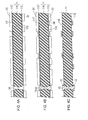
- FIG. 1 is a cross-sectional side view of a wiring substrate according to a first embodiment of the present invention
- FIG. 2 is a plan cross-sectional view of the wiring substrate
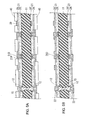
- FIG. 3A-3C are cross-sectional side views illustrating manufacturing processes of the wiring substrate
- FIG. 4A-4C are cross-sectional side views illustrating manufacturing processes of the wiring substrate
- FIG. 5A-5C are cross-sectional side views illustrating manufacturing processes of the wiring substrate
- FIG. 6A and 6B are cross-sectional side views illustrating manufacturing processes of the wiring substrate
- FIG. 7 is a cross-sectional side view illustrating a manufacturing process of the wiring substrate
- FIG. 8 is a cross-sectional side view illustrating a manufacturing process of the wiring substrate
- FIG. 9 is a cross-sectional side view illustrating a manufacturing process of the wiring substrate
- FIG. 10 is a cross-sectional side view of a wiring substrate according to a modified embodiment.
- FIG. 11 is a cross-sectional side view of a wiring substrate according to a modified embodiment.
- FIG. 1 in a wiring substrate 10 of the present embodiment, build-up layers 20 , 20 are respectively laminated on front and back surfaces of a core substrate 11 .
- the core substrate 11 is formed of an insulating member.
- a conductor circuit layer 12 (corresponding to a “conductor layer” of the present invention) is formed on each of an F surface ( 11 F), which is the front side surface of the core substrate 11 , and an S surface ( 11 S), which is the back side surface of the core substrate 11 .
- An electrical conduction through hole 14 is formed in the core substrate 11 .
- the electrical conduction through hole 14 is formed in a middle-constricted shape in which small diameter side ends of tapered holes ( 14 A, 14 A) are communicatively connected, the tapered holes ( 14 A, 14 A) being respectively formed by drilling from the F surface ( 11 F) and the S surface ( 11 S) of the core substrate 11 and being gradually reduced in diameter toward a deep side.
- the electrical conduction through hole 14 is filled with plating and a through-hole electrical conductor 15 is formed.
- the conductor circuit layer 12 on the F surface ( 11 F) and the conductor circuit layer 12 on the S surface ( 11 S) are connected by the through-hole electrical conductor 15 .
- Both the build-up layer 20 on the F surface ( 11 F) side of the core substrate 11 and the build-up layer 20 on the S surface ( 11 S) side are formed by sequentially laminating, the core substrate 11 side, a first insulating resin layer 21 , a first conductor layer 22 , a second insulating resin layer 23 and a second conductor layer 24 .
- a solder resist layer 25 is laminated on the second conductor layer 24 .
- the first insulating resin layer 21 and the second insulating resin layer 23 correspond to a “two-layer insulating layer” of the present invention.
- an F surface ( 10 F) which is a front side surface of the entire wiring substrate 10 , multiple pads are formed including a group of medium pads ( 26 A) and a group of small pads ( 26 C).
- the group of the small pads ( 26 C) is arrayed in a form of a matrix, and the group of the medium pads ( 26 A) is arrayed in a form of a frame surrounding the group of the small pads ( 26 C).
- pads on an S surface ( 10 S), which is a back side surface of the entire wiring substrate 10 are formed as large pads ( 26 B) that are larger than the medium pads ( 26 A).
- the via holes ( 21 H, 23 H) are all each formed in a tapered shape that is gradually reduced in diameter toward the core substrate 11 side.
- the via holes ( 21 H, 23 H) are filled with plating and multiple via conductors ( 21 D, 23 D) are formed. Then, the conductor circuit layer 12 and the first conductor layer 22 are connected by the via conductors ( 21 D) of the first insulating resin layer 21 ; and the first conductor layer 22 and the second conductor layer 24 are connected by the via conductors ( 23 D) of the second insulating resin layer 23 .
- a minimum width (W) of a wiring pattern and a minimum distance (H) between wiring patterns both are 15 pm or less. Further, a diameter of a lower portion (so-called via bottom) of each of the via conductors ( 21 D) connecting to the conductor circuit layer 12 and a diameter of a lower portion of each of the via conductors ( 23 D) connecting to the first conductor layer 22 both are 50 pm or less.
- the first insulating resin layer 21 and the second insulating resin layer 23 are each formed to have a two-layer structure that includes a support insulating layer 29 and a coating insulating layer 28 that is thicker than the support insulating layer 29 .
- the thickness of the support insulating layer 29 is 15-50% of the thickness of the coating insulating layer 28 .
- the coating insulating layer 28 is formed on the core substrate 11 side, and the support insulating layer 29 is formed on an outer side.
- the first conductor layer 22 or the second conductor layer 24 is formed on an upper surface of each of the support insulating layers 29 .
- the upper surfaces of the support insulating layers 29 are roughened surfaces. Further, the coating insulating layer 28 of the first insulating resin layer 21 covers the conductor circuit layer 12 on the core substrate 11 , and the coating insulating layer 28 of the second insulating resin layer 23 covers the first conductor layer 22 on the support insulating layer 29 of the first insulating resin layer 21 .
- the coating insulating layer 28 and the support insulating layer 29 both are formed from an insulating resin containing inorganic filler such as silica, alumina or mullite.
- inorganic filler such as silica, alumina or mullite.
- the content rate of the inorganic filler of the support insulating layer 29 is 42 wt % and the thermal expansion coefficient of the support insulating layer 29 is 39 ppm/° C.
- the content rate of the inorganic filler of the coating insulating layer 28 is 77 wt % and the thermal expansion coefficient of the coating insulating layer 28 is 12 ppm/° C.
- the content rate of the inorganic filler of the support insulating layer 29 is such a content rate that the thermal expansion coefficient of the coating insulating layer 28 is smaller than the thermal expansion coefficient of the support insulating layer 29 and the difference is 30 ppm/° C. or less.
- a thermal expansion coefficient of a conductor is 16.8 ppm/° C. That is, the difference between the thermal expansion coefficient of the via conductors ( 21 D, 23 D) and the thermal expansion coefficient of the coating insulating layer 28 is 10 ppm/° C.
- an average particle size of the inorganic filler in the support insulating layer 29 is 0.5 ⁇ m and a dielectric loss tangent (tan ⁇ ) (which indicates an electrical energy loss in an insulator) of the support insulating layer 29 is 0.017.
- an average particle size of the inorganic filler in the coating insulating layer 28 is 1.0 ⁇ m and a dielectric loss tangent (tan ⁇ ) of the coating insulating layer 28 is 0.0093.
- the coating insulating layer 28 and the support insulating layer 29 both do not contain a glass cloth.
- the wiring substrate 10 of the present embodiment is manufactured as follows.
- a substrate as the core substrate 11 is prepared that is obtained by laminating a copper foil ( 11 C) on both front and back surfaces of an insulating base material ( 11 K) that is formed of an epoxy resin or a BT (bismaleimide triazine) resin and a reinforcing material such as a glass cloth.
- a tapered hole ( 14 A) for forming the electrical conduction through hole 14 is drilled by irradiating, for example, CO2 laser to the core substrate 11 from the F surface ( 11 F) side.
- a tapered hole ( 14 A) is drilled on the S surface ( 11 S) side of the core substrate 11 by irradiating CO2 laser to a position directly on the back of the above-described tapered hole ( 14 A) on the F surface ( 11 F) side.
- the electrical conduction through hole 14 is formed from the tapered holes ( 14 A, 14 A).
- An electroless plating treatment is performed.
- An electroless plating film (not illustrated in the drawings) is formed on the copper foil ( 11 C) and on an inner surface of the electrical conduction through hole 14 .
- a plating resist 33 of a predetermined pattern is formed on the electroless plating film on the copper foil ( 11 C).
- An electrolytic plating treatment is performed. As illustrated in FIG. 4B , the electrical conduction through hole 14 is filled with electrolytic plating and the through-hole electrical conductor 15 is formed; and an electrolytic plating film 34 is formed on a portion of the electroless plating film (not illustrated in the drawings) on the copper foil ( 11 C), the portion being exposed from the plating resist 33 .
- the plating resist 33 is peeled off, and the electroless plating film (not illustrated in the drawings) and the copper foil ( 11 C), which are below the plating resist 33 , are removed.
- the conductor circuit layer 12 is formed on the F surface ( 11 F) of the core substrate 11
- the conductor circuit layer 12 is formed on the S surface ( 11 S) of the core substrate 11 .
- the conductor circuit layer 12 on the F surface ( 11 F) and the conductor circuit layer 12 on the S surface ( 11 S) are in a state of being connected by the through-hole electrical conductor 15 .
- an insulating sheet 30 obtained by integrally forming the coating insulating layer 28 and the support insulating layer 29 is laminated with the coating insulating layer 28 side facing downward, and then the resulting substrate is hot-pressed. In this case, spaces between portions of each conductor circuit layer ( 12 , 12 ) on the core substrate 11 are filled with the coating insulating layer 28 .
- the upper surface of the support insulating layer 29 is roughened using a chemical solution.
- multiple via holes ( 12 H) are formed by irradiating CO2 laser to the first insulating resin layers ( 21 , 21 ) on the front and back sides of the core substrate 11 . Some of the multiple via holes ( 21 H) are formed on the conductor circuit layer 12 .
- An electroless plating treatment is performed.
- An electroless plating film (not illustrated in the drawings) is formed on the first insulating resin layers ( 21 , 21 ) and in the via holes ( 21 H, 21 H).
- a plating resist 40 of a predetermined pattern is formed on the electroless plating film.
- the plating resist 40 is removed, and the electroless plating film (not illustrated in the drawings) that is below the plating resist 4 is removed.
- the first conductor layers 22 are respectively formed on the first insulating resin layers 21 on the front and back sides of the core substrate 11 by the remaining electrolytic plating films 39 and electroless plating film. Then, a state is achieved in which, on each of the front and back sides of the core substrate 11 , a portion of the first conductor layer 22 and the conductor circuit layer 12 are connected by the via conductors ( 21 D).
- solder resist layers ( 25 , 25 ) are respectively laminated on the second conductor layers 24 on the front and back sides of the core substrate 11 .
- pad holes are formed at predetermined places on the solder resist layers ( 25 , 25 ) on the front and back sides of the core substrate 11 , and portions of the second conductor layers 24 on the front and back sides of the core substrate 11 that are exposed from the pad holes become the pads 26 .
- the metal film 41 is not limited to the above-described Ni/Pd/Au, but may also be Ni/Au or Sn. It is also possible that an OSP film is formed instead of the metal film 41 .
- the description about the structure and the manufacturing method of the wiring substrate 10 of the present embodiment is as given above. Next, an example of use and an operation effect of the wiring substrate 10 are described.
- the wiring substrate 10 of the present embodiment is used, for example, by forming solder bumps (not illustrated in the drawings) on the pads 26 on the F surface ( 10 F) side and mounting and soldering a CPU or the like to the solder bumps, and soldering the pads 26 on the S surface ( 10 S) side to pads of a motherboard. In this case, some of pads of the CPU and some of the pads of the motherboard are connected via the via conductors ( 21 D, 23 D) of the wiring substrate 10 .
- the thermal expansion coefficient of the first insulating resin layer 21 is large (the difference between the thermal expansion coefficient of the first insulating resin layer 21 and the thermal expansion coefficient of the conductor is large)
- a problem can occur that a thermal stress acting on the via conductors ( 21 D) (in particular, the via bottom portions having the smallest diameter) is increased and the via conductors ( 21 D) are likely to peel off from the conductor circuit layer 12 below the via conductors ( 21 D).
- the thermal expansion coefficient of the coating insulating layer 28 of the first insulating resin layer 21 that is, the portion that covers the upper surface of the conductor circuit layer 12 and the periphery of the via bottoms of the via conductors ( 21 D) is small (the difference between the thermal expansion coefficient of the coating insulating layer 28 and the thermal expansion coefficient of the conductor is small). Therefore, that the via conductors ( 21 D) are peeled off from the conductor circuit layer 12 under the influence of thermal expansion of the first insulating resin layer 21 can be prevented, and reliability of the connection between the via conductors ( 21 D) and the conductor circuit layer 12 can be improved.
- the content rate of the inorganic filler in the entire first and second insulating resin layers ( 21 , 23 ) becomes large.
- a large amount of the inorganic filler also exists on the surfaces of the first and second insulating resin layers ( 21 , 23 ).
- the first insulating resin layer 21 and the second insulating resin layer 23 are each formed to have the two-layer structure that includes the coating insulating layer 28 having a relatively small thermal expansion coefficient (the content rate of the inorganic filler is large) and the support insulating layer 29 having a relatively large thermal expansion coefficient (the content rate of the inorganic filler is small). Then, the conductor layers ( 22 , 24 ) are each formed on the support insulating layer 29 , of which the content rate of the inorganic filler is smaller, among the coating insulating layer 28 and the support insulating layer 29 .
- the plating resist 40 can be densely formed, and a dense (fine) wiring pattern can be formed.
- the minimum width (W) of a wiring pattern and the minimum distance (H) between wiring patterns can both be reduced to 15 ⁇ m or less.
- the average particle size of the inorganic filler in the support insulating layer 29 is smaller than the average particle size of the inorganic filler in the coating insulating layer 28 . Therefore, adhesion of the plating resist 40 to the first and second insulating resin layers ( 21 , 23 ) can be further improved. Further, the upper surface of the support insulating layer 29 is a roughened surface. Therefore, the anchor effect during the formation of the plating resist 40 is further strengthened, and it becomes easy for the plating resist 40 to be densely formed. Further, fixing strength of the conductor layers ( 22 , 24 ) on the support insulating layers 29 is also increased.
- the thermal expansion coefficient of the first and second insulating resin layers ( 21 , 23 ) is large, due to expansion caused by heating and contraction caused by cooling, the entire wiring substrate 10 may warp.
- the first and second insulating resin layers ( 21 , 23 ) each have the coating insulating layer 28 that has a relatively small thermal expansion coefficient. Thereby, the thermal expansion coefficient of the entire first and second insulating resin layers ( 21 , 23 ) is reduced, and warpage of the entire wiring substrate 10 can be suppressed.
- the upper surface and the side surface of the wiring pattern are covered by the coating insulating layer 28 that has a smaller dielectric loss tangent (tans) than the support insulating layer 29 . Therefore, the electrical energy loss can be reduced as compared to a structure in which the wiring pattern is covered by the support insulating layer 29 only.
- a magnitude of a thermal conductivity varies depending on a magnitude of the content rate of the inorganic filler.
- the content rate of the inorganic filler is the same and the magnitude of the thermal conductivity is varied by varying the kind of the resin.
- the structure is adopted in which the insulating sheet 30 obtained by integrally forming the coating insulating layer 28 and the support insulating layer 29 is laminated.
- the coating insulating layer 28 and the support insulating layer 29 are separately laminated one by one.
- the content rate of the inorganic filler of the coating insulating layer 28 is 77 wt %, and the content rate of the inorganic filler of the support insulating layer 29 is 42 wt %.
- the present invention is not limited to this. It is preferable that the content rate of the inorganic filler of the coating insulating layer 28 be 65-85 wt %, and the content rate of the inorganic filler of the support insulating layer 29 be 30-50 wt %.
- two insulating resin layers are laminated on each of the front and back sides of the core substrate 11 .
- one insulating resin layer is laminated on each of the front and back sides of the core substrate 20 11 , or three or more insulating resin layers are laminated on each of the front and back sides of the core substrate 11 .
- all of the first and second insulating resin layers ( 21 , 23 ) are formed to have the two-layer structure that includes the coating insulating layer 28 and the support insulating layer 29 .
- no object is accommodated in the core substrate 11 .
- FIG. 10 it is also possible to adopt a structure in which a cavity 16 is formed in the core substrate 11 , and, for example, a metal block 17 is accommodated in the cavity 16 .
- FIG. 11 it is also possible to adopt a structure in which multiple cavities 16 are formed in the core substrate 11 , and electronic components such as a multilayer ceramic capacitor 18 are accommodated together with the metal block 17 in the cavities 16 .
- via conductors may peel off from conductor layers.
- a wiring substrate according to an embodiment of the present invention and a method for manufacturing a wiring substrate according to another embodiment of the present invention provide allow peeling of via conductors from a conductor layer to be suppressed and allow reliability of connection between the via conductors and the conductor layer to be improved.
- a wiring substrate includes: a core substrate; conductor layers and insulating resin layers that are alternately laminated on the core substrate, each of the insulating resin layers being a two-layer insulating layer including a support insulating layer and a coating insulating layer, one of the conductor layers being laminated on an upper surface of the support insulating layer, the coating insulating layer being stacked below the support insulating layer and covering one of the conductor layers below the coating insulating layer, and no conductor layer being laminated on an upper surface of the coating insulating layer; and via conductors that penetrate the two-layer insulating layers and connect the upper and lower conductor layers.
- the coating insulating layer and the support insulating layer respectively contain inorganic fillers at different content rates such that a thermal expansion coefficient of the coating insulating layer is smaller than a thermal expansion coefficient of the support insulating layer and a difference between the thermal expansion coefficients is 30 ppm/° C. or less.
- the content rate of the inorganic filler of the coating insulating layer is 65-85% by mass.
- the coating insulating layer is thicker than the support insulating layer.
Landscapes
- Engineering & Computer Science (AREA)
- Microelectronics & Electronic Packaging (AREA)
- Manufacturing & Machinery (AREA)
- Production Of Multi-Layered Print Wiring Board (AREA)
Applications Claiming Priority (2)
| Application Number | Priority Date | Filing Date | Title |
|---|---|---|---|
| JP2015-099629 | 2015-05-15 | ||
| JP2015099629A JP2016219478A (ja) | 2015-05-15 | 2015-05-15 | 配線基板及びその製造方法 |
Publications (2)
| Publication Number | Publication Date |
|---|---|
| US20160338195A1 US20160338195A1 (en) | 2016-11-17 |
| US9775237B2 true US9775237B2 (en) | 2017-09-26 |
Family
ID=57277463
Family Applications (1)
| Application Number | Title | Priority Date | Filing Date |
|---|---|---|---|
| US15/153,884 Active US9775237B2 (en) | 2015-05-15 | 2016-05-13 | Wiring substrate and method for manufacturing the same |
Country Status (2)
| Country | Link |
|---|---|
| US (1) | US9775237B2 (ja) |
| JP (1) | JP2016219478A (ja) |
Cited By (1)
| Publication number | Priority date | Publication date | Assignee | Title |
|---|---|---|---|---|
| US20220104352A1 (en) * | 2020-09-28 | 2022-03-31 | Shinko Electric Industries Co., Ltd. | Interconnect substrate and method of making the same |
Families Citing this family (11)
| Publication number | Priority date | Publication date | Assignee | Title |
|---|---|---|---|---|
| JP2015035496A (ja) * | 2013-08-09 | 2015-02-19 | イビデン株式会社 | 電子部品内蔵配線板の製造方法 |
| JP6444269B2 (ja) * | 2015-06-19 | 2018-12-26 | 新光電気工業株式会社 | 電子部品装置及びその製造方法 |
| JP6660850B2 (ja) * | 2016-08-05 | 2020-03-11 | 新光電気工業株式会社 | 電子部品内蔵基板及びその製造方法と電子部品装置 |
| US10602622B2 (en) * | 2017-10-27 | 2020-03-24 | Kyocera Corporation | Wiring board |
| JP2019207979A (ja) * | 2018-05-30 | 2019-12-05 | イビデン株式会社 | プリント配線板 |
| CN111640727B (zh) * | 2019-03-01 | 2022-09-23 | 奥特斯(中国)有限公司 | 包括具有不同物理特性的介电结构的部件承载件 |
| CN211045436U (zh) * | 2019-07-07 | 2020-07-17 | 深南电路股份有限公司 | 线路板 |
| JP7249907B2 (ja) * | 2019-08-08 | 2023-03-31 | 新光電気工業株式会社 | 配線基板の製造方法及び積層構造 |
| US11688668B2 (en) | 2019-12-31 | 2023-06-27 | At&S (China) Co. Ltd. | Component carrier with low shrinkage dielectric material |
| CN113130408A (zh) | 2019-12-31 | 2021-07-16 | 奥特斯奥地利科技与系统技术有限公司 | 部件承载件及制造部件承载件的方法 |
| US11540396B2 (en) * | 2020-08-28 | 2022-12-27 | Unimicron Technology Corp. | Circuit board structure and manufacturing method thereof |
Citations (9)
| Publication number | Priority date | Publication date | Assignee | Title |
|---|---|---|---|---|
| JP2001345560A (ja) | 2000-02-09 | 2001-12-14 | Ngk Spark Plug Co Ltd | 配線基板およびその製造方法、並びに電子部品 |
| US6869665B2 (en) * | 2002-09-26 | 2005-03-22 | Fujitsu Limited | Wiring board with core layer containing inorganic filler |
| US7294393B2 (en) * | 2002-12-27 | 2007-11-13 | Nec Corporation | Sheet material and wiring board |
| US7692103B2 (en) * | 2003-11-18 | 2010-04-06 | Ngk Spark Plug Co., Ltd. | Wiring substrate and manufacturing process of the same |
| US8318599B2 (en) * | 2006-02-21 | 2012-11-27 | Fujitsu Limited | Resin layer formation method and semiconductor device fabrication method |
| US8530751B2 (en) * | 2010-08-02 | 2013-09-10 | Ngk Spark Plug Co., Ltd. | Multilayer wiring substrate |
| US8802996B2 (en) * | 2010-08-31 | 2014-08-12 | Kyocera Corporation | Wiring board and mounting structure thereof |
| US9060455B2 (en) * | 2011-09-12 | 2015-06-16 | Shinko Electric Industries Co., Ltd. | Wiring board and method of manufacturing the same |
| US9091921B2 (en) * | 2010-02-08 | 2015-07-28 | Taiyo Holdings Co., Ltd. | Layered structure and photosensitive dry film to be used therefor |
Family Cites Families (7)
| Publication number | Priority date | Publication date | Assignee | Title |
|---|---|---|---|---|
| AU2002355051A1 (en) * | 2001-11-30 | 2003-06-10 | Ajinomoto Co., Inc. | Method of laminating circuit board and method of forming insulation layer, multilayer printed wiring board and production method therefor and adhesion film for multilayer printed wiring board |
| JP2004123874A (ja) * | 2002-10-01 | 2004-04-22 | Nippon Steel Chem Co Ltd | フィルム形成用樹脂組成物及びフィルム状接着剤 |
| JP5987314B2 (ja) * | 2011-12-27 | 2016-09-07 | イビデン株式会社 | プリント配線板 |
| WO2013161527A1 (ja) * | 2012-04-26 | 2013-10-31 | 日本特殊陶業株式会社 | 多層配線基板及びその製造方法 |
| JP6011079B2 (ja) * | 2012-07-05 | 2016-10-19 | 味の素株式会社 | 支持体付き樹脂シート |
| JP6162458B2 (ja) * | 2013-04-05 | 2017-07-12 | 新光電気工業株式会社 | 配線基板、半導体装置及び配線基板の製造方法 |
| JP2015008261A (ja) * | 2013-05-28 | 2015-01-15 | 京セラサーキットソリューションズ株式会社 | 配線基板およびその製造方法 |
-
2015
- 2015-05-15 JP JP2015099629A patent/JP2016219478A/ja active Pending
-
2016
- 2016-05-13 US US15/153,884 patent/US9775237B2/en active Active
Patent Citations (9)
| Publication number | Priority date | Publication date | Assignee | Title |
|---|---|---|---|---|
| JP2001345560A (ja) | 2000-02-09 | 2001-12-14 | Ngk Spark Plug Co Ltd | 配線基板およびその製造方法、並びに電子部品 |
| US6869665B2 (en) * | 2002-09-26 | 2005-03-22 | Fujitsu Limited | Wiring board with core layer containing inorganic filler |
| US7294393B2 (en) * | 2002-12-27 | 2007-11-13 | Nec Corporation | Sheet material and wiring board |
| US7692103B2 (en) * | 2003-11-18 | 2010-04-06 | Ngk Spark Plug Co., Ltd. | Wiring substrate and manufacturing process of the same |
| US8318599B2 (en) * | 2006-02-21 | 2012-11-27 | Fujitsu Limited | Resin layer formation method and semiconductor device fabrication method |
| US9091921B2 (en) * | 2010-02-08 | 2015-07-28 | Taiyo Holdings Co., Ltd. | Layered structure and photosensitive dry film to be used therefor |
| US8530751B2 (en) * | 2010-08-02 | 2013-09-10 | Ngk Spark Plug Co., Ltd. | Multilayer wiring substrate |
| US8802996B2 (en) * | 2010-08-31 | 2014-08-12 | Kyocera Corporation | Wiring board and mounting structure thereof |
| US9060455B2 (en) * | 2011-09-12 | 2015-06-16 | Shinko Electric Industries Co., Ltd. | Wiring board and method of manufacturing the same |
Cited By (2)
| Publication number | Priority date | Publication date | Assignee | Title |
|---|---|---|---|---|
| US20220104352A1 (en) * | 2020-09-28 | 2022-03-31 | Shinko Electric Industries Co., Ltd. | Interconnect substrate and method of making the same |
| US11617264B2 (en) * | 2020-09-28 | 2023-03-28 | Shinko Electric Industries Co., Ltd. | Interconnect substrate and method of making the same |
Also Published As
| Publication number | Publication date |
|---|---|
| JP2016219478A (ja) | 2016-12-22 |
| US20160338195A1 (en) | 2016-11-17 |
Similar Documents
| Publication | Publication Date | Title |
|---|---|---|
| US9775237B2 (en) | Wiring substrate and method for manufacturing the same | |
| US9955591B2 (en) | Circuit substrate and method for manufacturing the same | |
| US20100224397A1 (en) | Wiring board and method for manufacturing the same | |
| US10745819B2 (en) | Printed wiring board, semiconductor package and method for manufacturing printed wiring board | |
| US9693458B2 (en) | Printed wiring board, method for manufacturing printed wiring board and package-on-package | |
| KR100653249B1 (ko) | 메탈코어, 패키지 기판 및 그 제작방법 | |
| US10249561B2 (en) | Printed wiring board having embedded pads and method for manufacturing the same | |
| US11277925B2 (en) | Wiring board and method for manufacturing the same | |
| US10098243B2 (en) | Printed wiring board and semiconductor package | |
| US6711812B1 (en) | Method of making metal core substrate printed circuit wiring board enabling thermally enhanced ball grid array (BGA) packages | |
| US9601422B2 (en) | Printed wiring board, semiconductor package, and method for manufacturing printed wiring board | |
| JP2016201529A (ja) | 印刷回路基板、その製造方法、及び電子部品モジュール | |
| US10262930B2 (en) | Interposer and method for manufacturing interposer | |
| US20170033036A1 (en) | Printed wiring board, semiconductor package, and method for manufacturing printed wiring board | |
| US10186486B2 (en) | Wiring board | |
| JP6226168B2 (ja) | 多層配線板 | |
| US20170064825A1 (en) | Printed wiring board and method for manufacturing printed wiring board | |
| US8525041B2 (en) | Multilayer wiring board and method for manufacturing the same | |
| KR101167429B1 (ko) | 반도체 패키지의 제조방법 | |
| JP5176676B2 (ja) | 部品内蔵基板の製造方法 | |
| US10314168B2 (en) | Printed wiring board | |
| US20160353572A1 (en) | Printed circuit board, semiconductor package and method of manufacturing the same | |
| US11363719B2 (en) | Wiring substrate and component built-in wiring substrate | |
| US8125074B2 (en) | Laminated substrate for an integrated circuit BGA package and printed circuit boards | |
| JP2003229662A (ja) | 配線基板の製造方法 |
Legal Events
| Date | Code | Title | Description |
|---|---|---|---|
| AS | Assignment |
Owner name: IBIDEN CO., LTD., JAPAN Free format text: ASSIGNMENT OF ASSIGNORS INTEREST;ASSIGNOR:IKEDA, KOSUKE;REEL/FRAME:038586/0818 Effective date: 20160510 |
|
| STCF | Information on status: patent grant |
Free format text: PATENTED CASE |
|
| MAFP | Maintenance fee payment |
Free format text: PAYMENT OF MAINTENANCE FEE, 4TH YEAR, LARGE ENTITY (ORIGINAL EVENT CODE: M1551); ENTITY STATUS OF PATENT OWNER: LARGE ENTITY Year of fee payment: 4 |