US9590210B2 - Method of evaluating image blur of optical film and optical film with reduced image blur - Google Patents
Method of evaluating image blur of optical film and optical film with reduced image blur Download PDFInfo
- Publication number
- US9590210B2 US9590210B2 US14/513,393 US201414513393A US9590210B2 US 9590210 B2 US9590210 B2 US 9590210B2 US 201414513393 A US201414513393 A US 201414513393A US 9590210 B2 US9590210 B2 US 9590210B2
- Authority
- US
- United States
- Prior art keywords
- optical film
- refractive index
- layer
- emitting display
- organic light
- Prior art date
- Legal status (The legal status is an assumption and is not a legal conclusion. Google has not performed a legal analysis and makes no representation as to the accuracy of the status listed.)
- Active, expires
Links
- 239000012788 optical film Substances 0.000 title claims abstract description 165
- 238000000034 method Methods 0.000 title claims abstract description 24
- 230000035807 sensation Effects 0.000 claims abstract description 48
- 238000009826 distribution Methods 0.000 claims abstract description 24
- 238000012360 testing method Methods 0.000 claims abstract description 23
- 230000001131 transforming effect Effects 0.000 claims abstract description 4
- 239000000463 material Substances 0.000 claims description 27
- 230000010287 polarization Effects 0.000 claims description 26
- 239000010408 film Substances 0.000 claims description 25
- 239000011347 resin Substances 0.000 claims description 25
- 229920005989 resin Polymers 0.000 claims description 25
- 230000006870 function Effects 0.000 claims description 15
- 230000003287 optical effect Effects 0.000 claims description 15
- 238000002834 transmittance Methods 0.000 claims description 14
- 238000009792 diffusion process Methods 0.000 claims description 9
- 230000035945 sensitivity Effects 0.000 claims description 3
- 239000010410 layer Substances 0.000 description 187
- 230000006872 improvement Effects 0.000 description 13
- 238000006243 chemical reaction Methods 0.000 description 10
- 239000012790 adhesive layer Substances 0.000 description 8
- 239000000758 substrate Substances 0.000 description 7
- -1 acryl Chemical group 0.000 description 6
- 238000005094 computer simulation Methods 0.000 description 6
- 238000004519 manufacturing process Methods 0.000 description 5
- 239000004372 Polyvinyl alcohol Substances 0.000 description 4
- 239000003990 capacitor Substances 0.000 description 4
- 238000013461 design Methods 0.000 description 4
- 239000000049 pigment Substances 0.000 description 4
- 229920002451 polyvinyl alcohol Polymers 0.000 description 4
- 230000009467 reduction Effects 0.000 description 4
- 230000000007 visual effect Effects 0.000 description 4
- PXHVJJICTQNCMI-UHFFFAOYSA-N Nickel Chemical compound [Ni] PXHVJJICTQNCMI-UHFFFAOYSA-N 0.000 description 3
- 238000003848 UV Light-Curing Methods 0.000 description 3
- 239000006096 absorbing agent Substances 0.000 description 3
- 230000007423 decrease Effects 0.000 description 3
- 238000005516 engineering process Methods 0.000 description 3
- 238000005259 measurement Methods 0.000 description 3
- 239000004417 polycarbonate Substances 0.000 description 3
- 239000002952 polymeric resin Substances 0.000 description 3
- 238000003860 storage Methods 0.000 description 3
- 229920003002 synthetic resin Polymers 0.000 description 3
- 239000006229 carbon black Substances 0.000 description 2
- 238000012937 correction Methods 0.000 description 2
- 230000008021 deposition Effects 0.000 description 2
- 230000005281 excited state Effects 0.000 description 2
- 230000005283 ground state Effects 0.000 description 2
- 238000002347 injection Methods 0.000 description 2
- 239000007924 injection Substances 0.000 description 2
- 239000002245 particle Substances 0.000 description 2
- 229920003229 poly(methyl methacrylate) Polymers 0.000 description 2
- 239000004926 polymethyl methacrylate Substances 0.000 description 2
- 239000010409 thin film Substances 0.000 description 2
- 229920002284 Cellulose triacetate Polymers 0.000 description 1
- 239000004820 Pressure-sensitive adhesive Substances 0.000 description 1
- XUIMIQQOPSSXEZ-UHFFFAOYSA-N Silicon Chemical compound [Si] XUIMIQQOPSSXEZ-UHFFFAOYSA-N 0.000 description 1
- NNLVGZFZQQXQNW-ADJNRHBOSA-N [(2r,3r,4s,5r,6s)-4,5-diacetyloxy-3-[(2s,3r,4s,5r,6r)-3,4,5-triacetyloxy-6-(acetyloxymethyl)oxan-2-yl]oxy-6-[(2r,3r,4s,5r,6s)-4,5,6-triacetyloxy-2-(acetyloxymethyl)oxan-3-yl]oxyoxan-2-yl]methyl acetate Chemical compound O([C@@H]1O[C@@H]([C@H]([C@H](OC(C)=O)[C@H]1OC(C)=O)O[C@H]1[C@@H]([C@@H](OC(C)=O)[C@H](OC(C)=O)[C@@H](COC(C)=O)O1)OC(C)=O)COC(=O)C)[C@@H]1[C@@H](COC(C)=O)O[C@@H](OC(C)=O)[C@H](OC(C)=O)[C@H]1OC(C)=O NNLVGZFZQQXQNW-ADJNRHBOSA-N 0.000 description 1
- 230000001070 adhesive effect Effects 0.000 description 1
- 229910052782 aluminium Inorganic materials 0.000 description 1
- XAGFODPZIPBFFR-UHFFFAOYSA-N aluminium Chemical compound [Al] XAGFODPZIPBFFR-UHFFFAOYSA-N 0.000 description 1
- 239000011324 bead Substances 0.000 description 1
- 239000011230 binding agent Substances 0.000 description 1
- 230000005540 biological transmission Effects 0.000 description 1
- 230000008859 change Effects 0.000 description 1
- 239000003086 colorant Substances 0.000 description 1
- 230000006866 deterioration Effects 0.000 description 1
- 238000011161 development Methods 0.000 description 1
- 230000000694 effects Effects 0.000 description 1
- 230000005525 hole transport Effects 0.000 description 1
- AMGQUBHHOARCQH-UHFFFAOYSA-N indium;oxotin Chemical compound [In].[Sn]=O AMGQUBHHOARCQH-UHFFFAOYSA-N 0.000 description 1
- 239000011159 matrix material Substances 0.000 description 1
- 229910052751 metal Inorganic materials 0.000 description 1
- 239000002184 metal Substances 0.000 description 1
- 229910052759 nickel Inorganic materials 0.000 description 1
- 239000011368 organic material Substances 0.000 description 1
- 229920000515 polycarbonate Polymers 0.000 description 1
- 239000002861 polymer material Substances 0.000 description 1
- 239000000047 product Substances 0.000 description 1
- 229910052710 silicon Inorganic materials 0.000 description 1
- 239000010703 silicon Substances 0.000 description 1
- 239000011856 silicon-based particle Substances 0.000 description 1
- 239000002904 solvent Substances 0.000 description 1
- 239000013589 supplement Substances 0.000 description 1
- 238000012546 transfer Methods 0.000 description 1
- 239000012780 transparent material Substances 0.000 description 1
Images


Classifications
-
- H01L51/5275—
-
- G—PHYSICS
- G02—OPTICS
- G02B—OPTICAL ELEMENTS, SYSTEMS OR APPARATUS
- G02B5/00—Optical elements other than lenses
- G02B5/02—Diffusing elements; Afocal elements
-
- H—ELECTRICITY
- H10—SEMICONDUCTOR DEVICES; ELECTRIC SOLID-STATE DEVICES NOT OTHERWISE PROVIDED FOR
- H10K—ORGANIC ELECTRIC SOLID-STATE DEVICES
- H10K50/00—Organic light-emitting devices
- H10K50/80—Constructional details
- H10K50/85—Arrangements for extracting light from the devices
- H10K50/858—Arrangements for extracting light from the devices comprising refractive means, e.g. lenses
-
- G—PHYSICS
- G02—OPTICS
- G02B—OPTICAL ELEMENTS, SYSTEMS OR APPARATUS
- G02B27/00—Optical systems or apparatus not provided for by any of the groups G02B1/00 - G02B26/00, G02B30/00
- G02B27/32—Fiducial marks and measuring scales within the optical system
- G02B27/34—Fiducial marks and measuring scales within the optical system illuminated
-
- G—PHYSICS
- G02—OPTICS
- G02B—OPTICAL ELEMENTS, SYSTEMS OR APPARATUS
- G02B5/00—Optical elements other than lenses
- G02B5/02—Diffusing elements; Afocal elements
- G02B5/0205—Diffusing elements; Afocal elements characterised by the diffusing properties
- G02B5/021—Diffusing elements; Afocal elements characterised by the diffusing properties the diffusion taking place at the element's surface, e.g. by means of surface roughening or microprismatic structures
-
- G—PHYSICS
- G02—OPTICS
- G02B—OPTICAL ELEMENTS, SYSTEMS OR APPARATUS
- G02B5/00—Optical elements other than lenses
- G02B5/02—Diffusing elements; Afocal elements
- G02B5/0205—Diffusing elements; Afocal elements characterised by the diffusing properties
- G02B5/0236—Diffusing elements; Afocal elements characterised by the diffusing properties the diffusion taking place within the volume of the element
-
- G—PHYSICS
- G02—OPTICS
- G02B—OPTICAL ELEMENTS, SYSTEMS OR APPARATUS
- G02B5/00—Optical elements other than lenses
- G02B5/02—Diffusing elements; Afocal elements
- G02B5/0273—Diffusing elements; Afocal elements characterized by the use
- G02B5/0278—Diffusing elements; Afocal elements characterized by the use used in transmission
-
- G—PHYSICS
- G02—OPTICS
- G02B—OPTICAL ELEMENTS, SYSTEMS OR APPARATUS
- G02B5/00—Optical elements other than lenses
- G02B5/02—Diffusing elements; Afocal elements
- G02B5/0273—Diffusing elements; Afocal elements characterized by the use
- G02B5/0294—Diffusing elements; Afocal elements characterized by the use adapted to provide an additional optical effect, e.g. anti-reflection or filter
-
- H01L51/5265—
-
- H—ELECTRICITY
- H10—SEMICONDUCTOR DEVICES; ELECTRIC SOLID-STATE DEVICES NOT OTHERWISE PROVIDED FOR
- H10K—ORGANIC ELECTRIC SOLID-STATE DEVICES
- H10K50/00—Organic light-emitting devices
- H10K50/80—Constructional details
- H10K50/85—Arrangements for extracting light from the devices
- H10K50/852—Arrangements for extracting light from the devices comprising a resonant cavity structure, e.g. Bragg reflector pair
-
- H—ELECTRICITY
- H10—SEMICONDUCTOR DEVICES; ELECTRIC SOLID-STATE DEVICES NOT OTHERWISE PROVIDED FOR
- H10K—ORGANIC ELECTRIC SOLID-STATE DEVICES
- H10K59/00—Integrated devices, or assemblies of multiple devices, comprising at least one organic light-emitting element covered by group H10K50/00
- H10K59/80—Constructional details
- H10K59/875—Arrangements for extracting light from the devices
- H10K59/876—Arrangements for extracting light from the devices comprising a resonant cavity structure, e.g. Bragg reflector pair
-
- H—ELECTRICITY
- H10—SEMICONDUCTOR DEVICES; ELECTRIC SOLID-STATE DEVICES NOT OTHERWISE PROVIDED FOR
- H10K—ORGANIC ELECTRIC SOLID-STATE DEVICES
- H10K59/00—Integrated devices, or assemblies of multiple devices, comprising at least one organic light-emitting element covered by group H10K50/00
- H10K59/80—Constructional details
- H10K59/875—Arrangements for extracting light from the devices
- H10K59/879—Arrangements for extracting light from the devices comprising refractive means, e.g. lenses
-
- H—ELECTRICITY
- H10—SEMICONDUCTOR DEVICES; ELECTRIC SOLID-STATE DEVICES NOT OTHERWISE PROVIDED FOR
- H10K—ORGANIC ELECTRIC SOLID-STATE DEVICES
- H10K71/00—Manufacture or treatment specially adapted for the organic devices covered by this subclass
- H10K71/70—Testing, e.g. accelerated lifetime tests
-
- G—PHYSICS
- G01—MEASURING; TESTING
- G01J—MEASUREMENT OF INTENSITY, VELOCITY, SPECTRAL CONTENT, POLARISATION, PHASE OR PULSE CHARACTERISTICS OF INFRARED, VISIBLE OR ULTRAVIOLET LIGHT; COLORIMETRY; RADIATION PYROMETRY
- G01J1/00—Photometry, e.g. photographic exposure meter
- G01J1/42—Photometry, e.g. photographic exposure meter using electric radiation detectors
- G01J1/4209—Photoelectric exposure meters for determining the exposure time in recording or reproducing
Definitions
- the disclosure relates to a method of evaluating image blur of an optical film, an optical film for reducing color shift with reduced image blur and an organic light-emitting display apparatus including the optical film.
- An organic light-emitting diode typically includes an anode, an organic emission layer and a cathode.
- OLED organic light-emitting diode
- When a voltage is applied between the anode and the cathode holes are injected from the anode to the organic emission layer, and electrodes are injected from the cathode to the organic emission layer.
- the holes and electrons injected into the organic emission layer recombine in the organic emission layer and generate excitons, and light is generated as the excitons transfer from an excited state to a ground state.
- One of the technologies is to use a micro cavity structure that resonates light having a certain wavelength to increase an intensity of the light, and emits the light to the outside. That is, a distance between an anode and a cathode is designed to match a representative wavelength of each of red, green and blue, and thus, only light corresponding thereto is resonated to be emitted to the outside, and the other light is weakened. As a result, an intensity of the light emitted to the outside is strengthened and sharpened, thereby increasing luminance and color purity thereof. Furthermore, the increase of luminance may lead to low power consumption, thereby increasing lifespan of the OLED.
- wavelengths to be amplified are determined based on the thickness of an organic deposition material layer.
- a length of a light path changes at a lateral side, thereby causing an effect similar to a change of thickness of an organic deposition material layer. Therefore, the wavelengths to be amplified are changed.
- the maximum resolution wavelength becomes shorter, and thus color shift occurs as the maximum resolution wavelength decreases.
- the white color may become bluish at a lateral side due to blue shift phenomenon.
- an optical film for reducing color shift which may reduce an amount of color shift based on viewing angles and maintain high luminance in the center, may be provided to overcome problems due to the color shift.
- a high refractive index pattern layer and a low refractive index pattern layer may be attached to form a lens pattern to reduce an amount of white angle dependency (“WAD”) changes according to viewing angles.
- WAD white angle dependency
- the OLED typically includes multiple pixel units that emit light, light emitted from a pixel may spread to adjacent pixels due the optical film. Therefore, image blur may occur.
- a method of evaluating image blur of an optical film, an optical film for reducing color shift and an organic light-emitting display apparatus including the optical film and with reduced image blur.
- a method of evaluating image blur of an optical film includes: displaying a test pattern by driving an organic light-emitting display apparatus including the optical film; obtaining an image by capturing the test pattern using a digital camera; obtaining a spatial luminance distribution from the image; transforming the spatial luminance distribution into a sensation curve; and estimating a blur width from the sensation curve, in which the blur width is a distance between peaks having minimum negative values, from among a plurality of peaks of the sensation curve.
- an x-axis of the sensation curve may represent distance and a y-axis of the sensation curve may represent sensation, the plurality of peaks of the sensation curve may include a plurality of peaks in x-y coordinates.
- the blur width may be a distance between two peaks having minimum negative y-coordinate values, from among peaks of the sensation curve in a region where the x-coordinates are negative and a region where the x-coordinates are positive.
- the test pattern may be displayed on the optical film by a plurality of pixels disposed along a scanning line of a panel of the organic light-emitting display apparatus.
- the digital camera may include a charge coupled device (“CCD”) of the digital camera having a predetermined resolution which allows 30 or more CCD pixels to cover one pixel of the organic light-emitting display apparatus.
- CCD charge coupled device
- the spatial luminance distribution may be estimated using a spectro-radiometer.
- the spatial luminance distribution may be transformed into the sensation curve using a Fourier transform and a numerical computation program.
- the spatial luminance distribution may be transformed into a spatial frequency function using the Fourier transform, and may be transformed into the sensation curve by multiplying a color sensitivity function (“CSF”) by the spatial frequency function and using an inverse Fourier transform.
- CSF color sensitivity function
- the optical film may be an optical film for reducing color shift.
- the optical film may include a base layer, a high refractive optical diffusion layer disposed on the base layer, a high refractive resin layer disposed on the high refractive optical diffusion layer, and a low refractive resin layer disposed on the high refractive resin layer, where an optical pattern is defined in the low refractive resin layer.
- an optical film includes: a high refractive index pattern layer including a material having a refractive index greater than about 1, in which a first surface of the high refractive index pattern layer includes a pattern corresponding to a plurality of grooves, each having a curved groove surface, and each of the plurality of grooves has a depth greater than a width thereof; and a low refractive index pattern layer including a material having a refractive index less than the refractive index of the high refractive index pattern layer, where the low refractive index pattern layer includes protrusions corresponding to the plurality of grooves, where the optical film satisfies the following condition:
- each of the plurality of grooves may have a stripe shape which extends in a predetermined direction, and the plurality of grooves may be 1-dimensionally arranged.
- the material of the high refractive index pattern layer or the material of the low refractive index pattern layer may include a transparent resin material and a light diffuser.
- a lens pattern area, in which the plurality of grooves is defined, and a non-pattern area may be alternately disposed in the optical film.
- a width of the lens pattern area may be greater than a width of the non-pattern area.
- each of the plurality of grooves may have a dot shape and the plurality of grooves may be 2-dimensionally arranged.
- each of the plurality of grooves may have an oval shape.
- the plurality of grooves may be arranged without intervals in a first direction and may be spaced apart from each other at predetermined intervals in a second direction, which is perpendicular to the first direction.
- the protrusions may include a plurality of layers having different refractive indexes from each other.
- the optical film may further include an anti-reflection layer disposed on the second surface of the high refractive index pattern layer, and a circular polarization film or a transmittance adjusting layer disposed between the high refractive index pattern layer and the anti-reflection layer.
- an organic light-emitting display apparatus includes: an organic light-emitting display panel including a plurality of pixels including organic emission layers, each of which emits light of different wavelengths, where each of the plurality of pixels has a micro cavity structure configured to resonate light corresponding to one of the different wavelengths; and any one of the above-described optical film disposed on the organic light-emitting display panel.
- FIG. 1A is a graph showing color shift based on viewing angle in a display panel including an embodiment of an optical film for reducing color shift and in a display panel without the optical film (bare panel);
- FIG. 1B is exemplary view showing image blur in a display panel including the optical film and in a bare panel;
- FIG. 2 is a cross-sectional view of an embodiment of an organic light-emitting display apparatus including an optical film for evaluating the image blur;
- FIG. 3 illustrates a test pattern shown as a scanning line of a panel on the optical film
- FIG. 4 is a graph showing a luminance curve and a sensation curve for defining a blur width used in an embodiment of a method of evaluating the image blur, according to the invention
- FIG. 5 is a cross-sectional view of an embodiment of the optical film for evaluating the image blur
- FIG. 6 is a detailed perspective view of a lenticular lens pattern in the optical film of FIG. 5 ;
- FIG. 7 is a view of a sensation curve obtained from an first embodiment of the optical film
- FIG. 8 is a view of a sensation curve obtained in a second embodiment of the optical film.
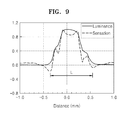
- FIG. 9 is a view of a sensation curve obtained in a third embodiment of the optical film.
- FIG. 10 is an image of a test pattern of the first embodiment captured using a digital camera
- FIG. 11 is an image of a test pattern of the second embodiment captured using the digital camera
- FIG. 12 is an image of a test pattern of the third embodiment captured using the digital camera
- FIG. 13 is an exploded perspective view of an embodiment of the optical film according to the invention.
- FIGS. 14 and 15 are cross-sectional views of embodiments of an optical film including an light diffuser, according to the invention.
- FIG. 16 is a cross-sectional view of an alternative embodiment of an optical film according to the invention.
- FIG. 17 is a plan view showing an arrangement relationship between the optical film of FIG. 16 and pixels of an embodiment of an organic light-emitting display panel including the optical film;
- FIG. 18 is an exploded perspective view of another alternative embodiment of an optical film according to the invention.
- FIG. 19 is a perspective view of a protrusion of the optical film of FIG. 18 ;
- FIGS. 20 and 21 are cross-sectional views of alternative embodiments of an optical film according to the invention.
- FIG. 22 is a cross-sectional view of another alternative embodiment of an optical film according to the invention.
- FIGS. 23 and 24 are cross-sectional views of embodiments of an optical film including a circular polarization film, according to the invention.
- FIG. 25 is a cross-sectional view of an embodiment of an optical film including a transmittance adjusting layer, according to the invention.
- FIG. 26 is a cross-sectional view of an embodiment of an organic light-emitting display apparatus according to the invention.
- first,” “second,” “third” etc. may be used herein to describe various elements, components, regions, layers and/or sections, these elements, components, regions, layers and/or sections should not be limited by these terms. These terms are only used to distinguish one element, component, region, layer or section from another element, component, region, layer or section. Thus, “a first element,” “component,” “region,” “layer” or “section” discussed below could be termed a second element, component, region, layer or section without departing from the teachings herein.
- relative terms such as “lower” or “bottom” and “upper” or “top,” may be used herein to describe one element's relationship to another element as illustrated in the Figures. It will be understood that relative terms are intended to encompass different orientations of the device in addition to the orientation depicted in the Figures. For example, if the device in one of the figures is turned over, elements described as being on the “lower” side of other elements would then be oriented on “upper” sides of the other elements. The exemplary term “lower,” can therefore, encompasses both an orientation of “lower” and “upper,” depending on the particular orientation of the figure.
- “About” or “approximately” as used herein is inclusive of the stated value and means within an acceptable range of deviation for the particular value as determined by one of ordinary skill in the art, considering the measurement in question and the error associated with measurement of the particular quantity (i.e., the limitations of the measurement system). For example, “about” can mean within one or more standard deviations, or within ⁇ 30%, 20%, 10%, 5% of the stated value.
- Exemplary embodiments are described herein with reference to cross section illustrations that are schematic illustrations of idealized embodiments. As such, variations from the shapes of the illustrations as a result, for example, of manufacturing techniques and/or tolerances, are to be expected. Thus, embodiments described herein should not be construed as limited to the particular shapes of regions as illustrated herein but are to include deviations in shapes that result, for example, from manufacturing. For example, a region illustrated or described as flat may, typically, have rough and/or nonlinear features. Moreover, sharp angles that are illustrated may be rounded. Thus, the regions illustrated in the figures are schematic in nature and their shapes are not intended to illustrate the precise shape of a region and are not intended to limit the scope of the claims.
- An optical film for reducing color shift may means an optical film that reduces white angle dependency (“WAD”) changes according to viewing angles, and thus allows the WAD according to the viewing angles to be substantially uniform.
- WAD white angle dependency
- an organic light-emitting display apparatus which typically includes a plurality of pixels, light emitted from a pixel may spread to adjacent pixels, and therefore, an image blur may occur.
- the image blur refers to a phenomenon where pixels are not clearly but hazily observed by a viewer.
- FIG. 1A is a graph showing color shift based on viewing angle in a display panel including an optical film for reducing color shift and in a display panel without such an optical film (hereinafter, will be referred to as a “bare panel”)
- FIG. 1B is exemplary view of image blur in a display panel including the optical film and in a bare panel.
- the rate ( ⁇ u′v′) of color shift based on the viewing angles is lower in a display panel including the optical film for reducing color shift than in the bare panel.
- the image blur may occur when the display panel includes the optical film for reducing color shift.
- Embodiment described herein may provide a method of objectively evaluating image blur in an optical film, more particularly, image blur in the optical film for reducing color shift, by quantifying the image blur.
- the method of evaluating the image blur of the optical film may include displaying a test pattern by driving an organic light-emitting display apparatus including the optical film, obtaining an image by capturing the test pattern using a digital camera, obtaining a spatial luminance distribution, obtaining a sensation curve by transforming the spatial luminance distribution, and estimating a blur width from the sensation curve.
- An embodiment of the method will hereinafter be described in greater detail with reference to FIGS. 2 and 3 .
- FIG. 2 is a cross-sectional view of an embodiment of an organic light-emitting display apparatus 200 including an optical film 100 for evaluating the image blur.
- FIG. 3 illustrates an embodiment of a test pattern for detecting image blur, displayed on the optical film 100 along a scanning line 10 of a panel of the organic light-emitting display apparatus 200 .
- the scanning line 10 may correspond to a plurality of pixels 11 sequentially disposed along a line in a predetermined direction.
- a test pattern of the panel is displayed on the optical film 100 as shown in FIG. 3 by driving the organic light-emitting display apparatus 200 including the optical film 100 of FIG. 2 .
- an image is obtained by capturing a test pattern using the digital camera.
- the digital camera may include a charge coupled device (“CCD”), and may have a predetermined resolution which allows 30 or more CCD pixels to cover each pixel 11 in the scanning line 10 on the organic light-emitting display apparatus 200 .
- CCD charge coupled device
- a relative spatial luminance distribution is obtained from the image obtained by capturing the test pattern. Then, the relative spatial luminance distribution is estimated or approximately calculated using a spectro-radiometer to obtain a front absolute luminance value. An actual spatial luminance distribution may be obtained from the relative spatial luminance distribution and the front absolute luminance value.
- the actual spatial luminance distribution obtained from the relative spatial luminance distribution and the front absolute luminance value may be transformed into a sensation curve using Fourier transform and a numerical computation program.
- the actual spatial luminance distribution is transformed into a spatial frequency function using Fourier transform
- the sensation curve may be obtained by multiplying a color sensitivity function (“CSF”) by the spatial frequency function and then applying an inverse Fourier transform to the product thereof.
- CSF color sensitivity function
- the Fourier transform may be fast Fourier transform (“FFT”) and may be conducted using a numerical computation program such as Mathematica® or Matlab®.
- FFT fast Fourier transform
- the image blur may be quantified based on parameters defined by a distance blur width as measured based on the sensation curve.
- the blur width may be defined as a distance between peaks having the minimum negative values from among a plurality of peaks of the sensation curve.
- FIG. 4 is a graph showing a luminance curve and a sensation curve for defining a blur width used in an embodiment of the method of evaluating the image blur according to the invention.
- the x-axis represents distance and the y-axis represents sensation
- the sensation curve includes a plurality of peaks according to x-coordinates and y-coordinates of the sensation curve.
- the blur width may be defined as a distance L between two peaks on the sensation curve, i.e., a peak having minimum negative y-coordinate value in a region where the x-coordinates are negative and a peak having minimum negative y-coordinate value in a region where the x-coordinates are positive.
- the blur width may be calculated by estimating the distance L between peaks having minimum negative y-coordinate values from among peaks having negative y-coordinate values.
- the optical film used for evaluating the image blur may be an optical film for reducing color shift.
- An embodiment of the optical film may include a base layer, a high refractive optical diffusion layer, a high refractive resin layer, and a low refractive resin layer including an optical pattern formed or defined thereon, which are sequentially disposed one on another.
- the high refractive optical diffusion layer may include a light diffuser
- the optical pattern may be a micro lens pattern or a lenticular lens pattern, for example.
- FIG. 5 is a cross-sectional view of an embodiment of the optical film for evaluating the image blur.
- FIG. 6 is a perspective view of a lenticular lens pattern in the optical film of FIG. 5 .
- a base layer 110 a high refractive optical diffusion layer 120 including a light diffuser 121 , a high refractive resin layer 130 , and a low refractive resin layer 140 including a lenticular lens pattern are sequentially disposed, e.g., stacked, one on another.
- the lenticular lens pattern may include a structure at a surface of the low refractive resin layer 140 which faces the high refractive resin layer 130 .
- the lenticular lens pattern may be provided or formed by disposing a plurality of lenticular lenses 143 on a low refractive resin layer 141 with intervals S, e.g., predetermined constant intervals.
- intervals S e.g., predetermined constant intervals.
- An embodiment of the method of evaluating the image blur according to the invention may be used to improve color shift and reduce image blur.
- a base film (a triacetyl cellulose (“TAC”) film of Fujifilm Co.) having a thickness of about 60 micrometers ( ⁇ m) is provided in the organic light-emitting display apparatus (hereinafter, first embodiment). Then, according to a method described above, a sensation curve was obtained and a blur width was estimated, the results of which are shown in Table 1 below.
- FIG. 7 is a view of the sensation curve of the first embodiment
- FIG. 10 is an image of a test pattern of the first embodiment captured using a digital camera (NX20 of Samsung Electronics Co., Ltd.).
- the optical film of FIG. 5 for reducing color in which layers described above with reference to FIG. 5 are sequentially stacked one on another, is provided in the organic light-emitting display apparatus (hereinafter, a second embodiment). Then, according to the method described above, a sensation curve was obtained and a blur width was estimated, the results of which are shown in Table 1 below.
- FIG. 8 is a view of the sensation curve of the second embodiment
- FIG. 11 is an image of a test pattern of the second embodiment captured using the digital camera (NX20 of Samsung Electronics Co., Ltd.).
- the TAC film of Fujifilm Co. is used as the base layer, and a thickness thereof is about 60 ⁇ m.
- the high refractive optical diffusion layer is an organic light diffuser which is manufactured using an ultraviolet (“UV”) curable transparent acryl-based resin (RS1400 of Aekyung Chemical Co., Ltd.), throughout which about 0.5 wt % of non-coated silicon-based particles (SL-200 of Cheil Industries Inc.) and about 0.5 wt % of acryl-based particles coated with a black pigment (xx-2740Z of Sekisui Chemical Co., Ltd.) are dispersed.
- the high refractive optical diffusion layer has a refractive index of about 1.528 and a thickness of about 40 ⁇ m.
- the high refractive resin layer is a transparent acryl-based UV curing resin, and has a refractive index of about 1.4 and a maximum thickness of about 40 ⁇ m.
- an optical pattern is defined or formed in the low refractive resin layer.
- the low refractive resin layer is formed using transparent acryl-based UV curing resin having a refractive index as shown in Table 1.
- a plurality of half-circular lenticular lenses is sequentially arrayed at intervals of about 18 ⁇ m on a surface of the low refractive resin layer.
- the low refractive resin layer and lenticular lenses are integrally formed.
- the low refractive resin layer has a thickness of about 17 ⁇ m, and the lenticular lenses each have a width D of about 10 ⁇ m, a height H of about 12 ⁇ m, and an aspect ratio (H/D) of about 1.2.
- FIG. 9 is a view of the sensation curve of the third embodiment
- FIG. 12 is an image of a test pattern of the third embodiment captured using the digital camera (NX20 of Samsung Electronics Co., Ltd.).
- the organic light-emitting display apparatus including the optical film according to the first to third embodiments is driven to display the test pattern shown as the scanning line of the panel on the optical film. Then, the image is obtained by capturing the test pattern using the digital camera. The relative spatial luminance distribution is obtained from the image using Origin, which is an image-luminance conversion program. Then, the absolute luminance value of the front is obtained using a spectro-radiometer (SR-UL2-CAL of Topcon Co.) to thus obtain the actual spatial luminance value.
- Origin which is an image-luminance conversion program.
- the spatial luminance value is fast Fourier transformed to obtain the spatial frequency function.
- the CSF which reflects visual characteristics of a spatial frequency
- the sensation curve is inverse Fourier transformed into a spatial function.
- a distance between left and right peaks on the sensation curve which have the minimum negative y-coordinate values from among peaks having negative y-coordinate values is calculated to thus estimate the blur width.
- the blur width is a parameter that reflects visual characteristics of the optical film for reducing color shift related to the image blur, in an embodiment, an actual degree of image blur that is sensed by eye may be effectively quantified.
- a blur width ratio (“BWR”) is defined by comparing an organic light-emitting display panel that does not include the optical film for reducing color shift and an organic light-emitting display panel that includes the optical film for reducing color shift as in the following Equation 1,
- Equation 1 L B denotes a blur width of the organic light-emitting display panel including the optical film for reducing color shift, and L B,0 denotes the blur width of the organic light-emitting display panel not including the optical film for reducing color shift.
- the optical film for reducing color shift may be designed to allow the BWR to be less than about 70%, and the color shift improvement rate to be maintained at about 35% or higher.
- an embodiment of the method of evaluating the image blur, which is quantified in terms of visual characteristics is provided.
- a structure of the optical film for reducing color shift with reduced image blur may be determined.
- the optical film is designed to maintain a color shift improvement rate of at least about 35%, and elements that affect improvement of the image blur when the color shift improvement rate of at least about 35% is maintained will be described.
- FIG. 13 is an exploded perspective view of an embodiment of an optical film 1 according to the invention.
- the optical film 1 includes a high refractive index pattern layer 1100 that includes a material having a refractive index greater than about 1 and further includes a plurality of grooves GR, each defined by an engraved pattern of which a depth is greater than a width; and a low refractive index pattern layer 1200 that includes a material having a refractive index less than the refractive index of the material of the high refractive index pattern layer 1100 and further includes protrusions P that correspond to the plurality of grooves GR.
- the optical film 1 may satisfy a predetermined condition, e.g., an inequality below.
- L B denotes a blur width of an organic light-emitting display panel including the optical film 1
- L B,0 denotes a blur width of an organic light-emitting display panel not including the optical film, which are evaluated by the method described above.
- the plurality of grooves GR may be provided or formed to have a stripe shape that extends in a predetermined direction and be 1-dimensionally arranged at predetermined intervals T1.
- the aspect ratio i.e., a ratio of a width “w” of a groove to a depth “d” of the groove, a difference ⁇ n between a refractive index of the high refractive index pattern layer 1100 and a refractive index of the low refractive index pattern layer 1200 , and the intervals T1 between the grooves GR are design variables that affect the color shift correction rate of the optical film 1 and the BWR defined by Equation 1.
- a large aspect ratio may be effective for reducing color shift, but may cause manufacturing difficulty and increase image blur.
- Table 2 is a computer simulation result showing BWRs corresponding to various values of the design variables.
- a pattern occupying ratio is set to be about 35% and a color shift improvement rate is set to be about 35%. From the computer simulation result, it may be understood that an appropriate aspect ratio and the difference ⁇ n between the refractive index of the high refractive index pattern layer 1100 and the refractive index of the low refractive index pattern layer 1200 may be determined for a stripe pattern in an optical film having the stripe pattern by considering an image blur and the color correction rate.
- FIG. 14 is a cross-sectional view of an embodiment of an optical film 2 including a light diffuser 1125 , according to the invention.
- the optical film 2 includes a high refractive index pattern layer 1120 , which includes a transparent resin material and a light diffuser 1125 , and the low refractive index pattern layer 1200 .
- the light diffuser 1125 may include diffusive beads, a silicon-based diffuser and/or an acryl-based diffuser, for example.
- the light diffuser 1125 increases visual characteristics by planarizing a peak that may occur in color shift ( ⁇ u′v′) and luminance profiles with respect to viewing angles.
- a content of the light diffuser 1125 may affect a degree of image blur.
- Table 3 is a computer simulation result of BWRs according to the content of the light diffuser 1125 .
- the computer simulation result shows that an optical film with reduced image blur may be prepared by providing the content of the light diffuser 1125 in the optical film to be about 1 wt % or less, thus planarizing peaks that may occur in color shift or the luminance profiles.
- a light diffuser may be included in a high refractive index pattern layer, but not being limited thereto. In an alternative embodiment, the light diffuser may be included in a low refractive index pattern layer.
- FIG. 15 is a cross-sectional view of an alternative embodiment of an optical film 3 including a light diffuser 1235 , according to the invention.
- the optical film 3 includes a high refractive index pattern layer 1100 and a low refractive index pattern layer 1230 , which includes a transparent resin material and a light diffuser 1235 .
- FIG. 16 is a cross-sectional view of an alternative embodiment of an optical film 4 according to the invention.
- FIG. 17 is a plan view of an arrangement relationship between the optical film 4 of FIG. 16 and pixels of an embodiment of an organic light-emitting display panel OP.
- the optical film 4 includes a high refractive index pattern layer 1140 including a lens pattern area A1 and a non-pattern area A2 that are alternately disposed with each other.
- the lens pattern area A1 includes a plurality of grooves GR which have a depth greater than a width thereof and are engraved therein, and a low refractive index pattern layer 1240 including a material having a refractive index less than that of the high refractive index pattern layer 1140 , where the low refractive index pattern layer 1240 includes protrusions P that correspond to the plurality of grooves GR.
- the lens pattern area A1 is an area for reducing color shift based on viewing angles by combining light incident from various incident angles.
- the plurality of grooves GR are alternately disposed at predetermined intervals T1 in the lens pattern area A1.
- the non-pattern area A2 is an area for reducing image distortion that may occur due to the lens pattern area A1.
- the lens pattern area A1 and the non-pattern area A2 may be alternately with each other, and each of the lens pattern area A1 and the non-pattern area A2 may be disposed at predetermined intervals T2.
- the intervals T2 in which the lens pattern area A1 and the non-pattern area A2 are alternately or adjacently disposed, and respective widths of the lens pattern area A1 and the non-pattern area A2 may be based on a pixel arrangement of a display panel on which the optical film 4 is attached. As illustrated in FIG. 17 , the optical film 4 may be attached on the organic light-emitting display panel OP.
- the organic light-emitting display panel OP includes light emission areas corresponding to a plurality of pixels (e.g., a red pixel R, a green pixel G, a blue pixel B) and non-emission areas between the light emission areas.
- the intervals T2 and the respective widths of the lens pattern area A1 and the non-pattern area A2 may be determined to allow the lens pattern area A1 to be disposed at a location facing an emission area and the non-pattern area A2 to be disposed at a location facing at least a portion of the non-emission area.
- the non-pattern area A2 reduces the image distortion that may occur due to the lens pattern area A1. Accordingly, in such an embodiment, if a width S2 of the non-pattern area A2 is too large, color shift reduction by the optical film 4 may be relatively ineffective, and if the width S2 of the non-pattern area A2 is too small, image distortion may occur. Therefore, in an embodiment, widths of the S1 and S2 are predetermined to optimize color shift reduction and image distortion reduction. If S2/S1 decreases, image blur is reduced, but a degree of color shift improvement may also decrease. If S2/S1 increases, a degree of color shift improvement may increase (i.e., color shift is reduced), but image blur is also increased. An appropriate range of S2/S1 may be determined based on predetermined degrees of color shift improvement and image distortion.
- FIG. 18 is an exploded perspective view of another alternative embodiment of an optical film 5 according to the invention.
- FIG. 19 is a perspective view of a protrusion P of the optical film 5 of FIG. 18 .
- the optical film 5 includes a high refractive index pattern layer 1150 including a pattern defined by a plurality of grooves GR, and a low refractive index pattern layer 1250 including protrusions P that correspond to the plurality of grooves GR.
- the plurality of grooves GR may be 2-dimensionally arranged in two directions that are perpendicular to each other, and each of the plurality of grooves GR may have a dot shape.
- the plurality of grooves GR are arranged without intervals in one of the two directions, but are spaced apart from each other at the predetermined intervals T1 in the other direction.
- each of the protrusions P may have an oval shape as illustrated in FIG. 19 .
- An aspect ratio “c/2a,” a long axis length “2b,” and a short axis length “2a” may be appropriately determined for each of the protrusions P to reduce color shift and image blurs as described above.
- Table 4 is a computer simulation result of BWRs and color shift improvement rates according to various forms of the oval shape and pattern occupying ratios.
- Table 4 shows increased reduction in the BWRs and color shift improvement rates.
- the BWRs may be effectively reduced by using a 2-dimensionally arranged dot patterns that are arranged without intervals in one direction.
- FIGS. 20 and 21 are cross-sectional views of alternative embodiments of an optical film 7 according to the invention.
- an embodiment of the optical film 6 includes the high refractive index pattern layer 1100 and the low refractive index pattern layer 1200 .
- the high refractive index pattern layer 1100 includes a pattern defined by the plurality of grooves GR that are engraved on a surface thereof, and the low refractive index pattern layer 1200 includes protrusions corresponding to the plurality of grooves GR.
- the low refractive index pattern layer 1260 may include a plurality of layers having different refractive indexes as shown in FIG. 21 .
- an adhesive property between the low refractive index pattern layer 1200 and the high refractive index pattern layer 1100 may increase.
- color shift may be reduced based on refractive index difference between the low refractive index pattern layer 1200 and the high refractive index pattern layer 1100 .
- image blur may increase. Therefore, in such an embodiment, surface energy difference at a boundary surface is reduced by a gradual refractive index distribution, thereby increasing reliability and improving image blur.
- the low refractive index pattern layer 1200 may include a first layer 1250 and a second layer 1260 .
- the low refractive index pattern layer 1200 is not limited thereto, and the low refractive index pattern layer 1200 may include three or more layers.
- Embodiments of the optical film 1 to 7 described above may further include an adhesive layer, a circular polarization film, or a transmittance adjusting layer, for example, when the optical films 1 to 7 are applied to the organic light-emitting display apparatus.
- an adhesive layer for example, when the optical films 1 to 7 are applied to the organic light-emitting display apparatus.
- a circular polarization film for example, when the optical films 1 to 7 are applied to the organic light-emitting display apparatus.
- a transmittance adjusting layer for example, when the optical films 1 to 7 are applied to the organic light-emitting display apparatus.
- FIG. 22 is a cross-sectional view of another embodiment of an optical film 10 according to the invention.
- the optical film 10 further includes an anti-reflection layer 1900 disposed on the high refractive index pattern layer 1100 , a first adhesive layer 1310 disposed below the low refractive index pattern layer 1200 , and a first base layer 1410 disposed between the high refractive index pattern layer 1100 and the anti-reflection layer 1900 .
- the first adhesive layer 1310 which is for attaching the optical film 10 to the organic light-emitting display panel, may include or be formed of a pressure sensitive adhesive (“PSA”), or a PSA including a light absorber or a light diffuser, for example.
- PSA pressure sensitive adhesive
- the high refractive index pattern layer 1100 and/or low refractive index pattern layer 1200 may include a transparent material including a light absorber. In an embodiment, where a material including a light absorber is included in various layers in the optical film, external light reflection may be effectively reduced, thereby increasing visibility.
- the first base layer 1410 functions as a base substrate for forming the high refractive index pattern layer 1100 and the low refractive index pattern layer 1200 during a manufacturing process of the optical film 10 , and may include or be formed of an optically isotropic material such as TAC.
- FIGS. 23 and 24 are cross-sectional views of embodiments of an optical film 11 and 12 including the circular polarization film, according to the invention.
- the circular polarization film may include a phase conversion layer 1500 and a linear polarization layer 1600 .
- the phase conversion layer 1500 may be, for example, a ⁇ /4 retardation film.
- the linear polarization layer 1600 may include a polyvinyl alcohol (“PVA”) film, or may have a stacked structure including a TAC film or various other structures.
- PVA film polarizes light and may further include a dichromatic pigment absorbed to PVA, which is a polymer material.
- an embodiment of the optical film 11 or 12 includes the first adhesive layer 1310 , the low refractive index pattern layer 1200 , the high refractive index pattern layer 1100 , the phase conversion layer 1500 , the linear polarization layer 1600 , the first base 1410 and the anti-reflection layer 1900 , which are sequentially stacked one on another or sequentially disposed from the bottom to the top thereof.
- the circular polarization film including the phase conversion layer 1500 and the linear polarization layer 1600 reduces external light reflection to thereby increase visibility.
- the external light is changed to linear polarized light by passing through the linear polarization layer 1600 and is changed circularly polarized light by passing through the phase conversion layer 1500 .
- the circularly polarized light passes through the high refractive index pattern layer 1100 , the low refractive index pattern layer 1200 and the first adhesive layer 1310 , and is reflected from an interface of an organic light-emitting display panel (not shown) that contacts the first adhesive layer 1310 , and thereby the circularly polarization direction thereof is inversed or changed oppositely.
- the inversed circularly polarized light is changed to linearly polarized light that is perpendicular to a transmission axis of the linear polarization layer 1600 by passing through the phase conversion layer 1500 , thereby effectively prevented from being emitted to the outside.
- the high refractive index pattern layer 1100 may include or be formed of an isotropic material having an optic axis that is the same as that of the circular polarization film, such as TAC or solvent casted polycarbonate (“PC”).
- the optical film 12 may further include a second base layer 1420 and a second adhesive layer 1320 that are disposed between the high refractive index pattern layer 1100 and the phase conversion layer 1500 , and are sequentially disposed from the high refractive index pattern layer 1100 toward the phase conversion layer 1500 .
- FIG. 25 is a cross-sectional view of an embodiment of an optical film 13 including a transmittance adjusting layer 1700 , according to the invention.
- the transmittance adjusting layer 1700 may be a film formed by dispersing in polymer resin a light absorbing black material such as a black dye, a pigment, carbon black, or bridging particles on which a black dye, a pigment, or carbon black is coated.
- the polymer resin may be, but is not limited to, a binder such as polymethyl methacrylate (“PMMA”), or an acryl-based UV curing resin.
- a thickness of the transmittance adjusting layer 1700 or a content of black materials in the polymer resin may be determined based on optical properties of the black materials.
- a transmittance of the transmittance adjusting layer 1700 may be about 40% or above, which is slightly greater than a transmittance of the circular polarization film.
- the transmittance adjusting layer 1700 supplements the circular polarization film which completely blocks external light but has a low transmittance.
- the optical film 13 includes the first adhesive layer 1310 , the low refractive index pattern layer 1200 , the high refractive index pattern layer 1100 , a first carrier film 1810 , the transmittance adjusting layer 1700 and the anti-reflection layer 1900 , which are sequentially stacked one on another or sequentially disposed from the bottom to the top thereof.
- the first carrier film 1810 functions as a base substrate for forming the high refractive index pattern layer 1100 and the low refractive index pattern layer 1200 during a manufacturing process of the optical film 13 , or as a base for forming the anti-reflection layer 1900 and the transmittance adjusting layer 1700 .
- the optical film 13 may not include a linear polarization layer and may not need to maintain polarization, such that the optical film 13 may include any of various materials including TAC, PET and PC, for example.
- respective shapes of the high refractive index pattern layer 1100 and the low refractive index pattern layer 1200 are substantially the same as in the embodiments of the optical film 1 described above with reference to FIG. 13 .
- the respective shapes are not limited thereto, and may be variously modified, e.g., may be changed to the shapes illustrated in FIGS. 14 to 21 .
- Respective arrangement structures of the embodiments of the optical films 10 to 14 described above with reference to FIGS. 22 to 25 may be changed to various other arrangements.
- respective locations of the phase conversion layer 1500 and the linear polarization layer 1600 included in the circular polarization film may be changed, or another layer may be further disposed between the phase conversion layer 1500 and the linear polarization layer 1600 .
- a second base layer and a second carrier film may be additionally included.
- the embodiments of the optical film described above may be used in the organic light-emitting display apparatus.
- the organic light-emitting display apparatus may include an organic emission layer having a micro cavity structure configured to enhanced color purity, and color shift based on the viewing angles may be reduced, thereby providing a high-quality image with reduced image blur.
- FIG. 26 is a cross-sectional view of an embodiment of an organic light-emitting display apparatus 500 according to the invention.
- the organic light-emitting display apparatus 500 includes an organic light-emitting display panel 510 , and an optical film 520 disposed on the organic light-emitting display panel 510 .
- the organic light-emitting display panel 510 includes a plurality of pixels including organic emission layers that emit light having different wavelengths, and each of the organic emission layers includes a micro cavity structure that resonates light having corresponding wavelength.
- the optical film 520 of the organic light-emitting display apparatus 500 may be substantially the same as the optical film 12 shown in FIG. 24 .
- the optical film 520 of the organic light-emitting display apparatus 500 is not limited thereto, and other embodiments of the optical film as described herein may be used.
- the organic light-emitting display panel 510 has a micro cavity structure to increase luminance and color purity.
- the organic light-emitting display panel 510 includes a plurality of OLEDs, each of which emits one of red (R), green (G) and blue (B) light, or white color light.
- Each OLED includes an anode 23 , an organic emission layer 24 and a cathode 25 . In an embodiment, as illustrated in FIG.
- the organic light-emitting display panel 510 may include an OLED corresponding to a unit pixel which emits one of red (R), green (G) and blue (B) light, and have the micro cavity structure in which a distance between the anode 23 and the cathode 25 of a red OLED having a long wavelength is relatively the longest, and that a distance between the anode 23 and the cathode 25 of a blue OLED having a short wavelength is relatively the shortest.
- R red
- G green
- B blue
- a distance between the anode 23 and the cathode 25 is set to correspond to respective representative wavelengths of R, G and B such that only light corresponding to the respective representative wavelengths is resonated and externally output while other light is weakened.
- Each sub-pixel of the organic light-emitting display panel 510 may include the OLED that is disposed between a first substrate 21 and a second substrate 29 facing each other, where the OLED includes the anode 23 , the organic emission layer 24 and the cathode 25 , and a driver circuit unit 22 that is disposed on the first substrate 21 and is electrically connected to the anode 23 and the cathode 25 .
- the anode 23 may include or be formed of an opaque metal such as aluminum (Al), and the cathode 25 may include or be formed of a transparent electrode such as indium tin oxide (“ITO”) or a semitransparent electrode such as nickel (Ni) thin film such that light emitted from the organic emission layer 24 is transmitted.
- a transparent electrode such as indium tin oxide (“ITO”) or a semitransparent electrode such as nickel (Ni) thin film such that light emitted from the organic emission layer 24 is transmitted.
- the driver circuit unit 22 may include at least two thin film transistors (“TFT”s) (not shown) and a capacitor (not shown), and controls luminance of the OLED by controlling an amount of current supplied to the OLED based on data signals.
- TFT thin film transistors
- the driver circuit unit 22 which may be a circuit for driving unit pixels of the organic light-emitting display panel 510 , may include a gate line, a data line vertically crossing the gate line, a switching TFT connected to the gate line and the data line, a driving TFT connected to the OLED and disposed between the switching TFT and a power line, and a storage capacitor connected between a gate electrode of the driving TFT and the power line.
- the switching TFT responds to (e.g., is turned on or off based on) scan signals of the gate line, and thus supplies data signals of the data line to the gate electrode of the driving TFT and the storage capacitor.
- the driving TFT responds to the data signals from the switching TFT, controls current supplied to the OLED from the power line, and thus controls the luminance of the OLED.
- the storage capacitor stores the data signals from the switching TFT as stored voltages, and supplies stored voltages to the driving TFT such that the driving TFT may constantly supply current even when the switching TFT is turned off.
- the organic emission layer 24 includes a hole injection layer (“HIL”), a hole transport layer (“HTL”), a light-emitting layer, an electron transport layer (“ETL”), and an electron injection layer (“EIL”) that are sequentially stacked on the anode 23 .
- HIL hole injection layer
- HTL hole transport layer
- ETL electron transport layer
- EIL electron injection layer
- the electrons and holes injected into the light-emitting layer L recombine in the light-emitting layer and generate excitons, and light is emitted as the excitons are shifted from an excited state to a ground state.
- a luminance of the emitted light is substantially proportional to an amount of current flowing between the anode 23 and the cathode 25 .
- the organic light-emitting display panel 510 may include a color filter 27 to increase color efficiency.
- the color filter 27 is disposed on the second substrate 29 .
- a red color filter is disposed in a red sub-pixel area
- a green color filter is disposed in a green sub-pixel area
- a blue color filter is disposed in a blue color filter area.
- the color filter 27 may be not included in a white sub-pixel area.
- a black matrix may be disposed on the second substrate 29 at a boundary of each sub-pixel to shield light and prevent mixing of colors.
- maximum resonant wavelength becomes shorter, that is, color shift occurs toward the short wavelength, by a tilt in the viewing angle from the front to a lateral side.
- white light may be observed at the front, but a blue color shift in which bluish white light is observed may occur at the lateral side.
- the optical film 520 is disposed on the organic light-emitting display panel 510 to reduce color shift.
- the optical film 520 includes a lens pattern defined by the high refractive index pattern layer 1100 and the low refractive index pattern layer 1200 to reduce color shift.
- design details of the lens pattern may be determined to reduce image blur due to the lens pattern.
- the high refractive index pattern layer 1100 and the low refractive index pattern layer 1200 may be variously configured as described above with reference to FIGS. 13 to 20 .
- the high refractive index pattern layer 1100 and the low refractive index pattern layer 1200 receive light that is incident at a certain angle and emit light at various angles and function as color shift reducing layers.
- Light output from the organic light-emitting display panel 510 has a predetermined angle distribution at which light is emitted and has a color shift that varies according to the angle.
- a distance from the organic emission layer 24 to the optical film 520 may be set to be about 1.5 millimeters (mm) or less to reduce image distortions.
Applications Claiming Priority (2)
| Application Number | Priority Date | Filing Date | Title |
|---|---|---|---|
| KR10-2013-0122820 | 2013-10-15 | ||
| KR1020130122820A KR102120809B1 (ko) | 2013-10-15 | 2013-10-15 | 광학필름의 이미지 블러 평가 방법 및 이미지 블러가 감소된 광학 필름 |
Publications (2)
| Publication Number | Publication Date |
|---|---|
| US20150103338A1 US20150103338A1 (en) | 2015-04-16 |
| US9590210B2 true US9590210B2 (en) | 2017-03-07 |
Family
ID=52809403
Family Applications (1)
| Application Number | Title | Priority Date | Filing Date |
|---|---|---|---|
| US14/513,393 Active 2034-10-18 US9590210B2 (en) | 2013-10-15 | 2014-10-14 | Method of evaluating image blur of optical film and optical film with reduced image blur |
Country Status (2)
| Country | Link |
|---|---|
| US (1) | US9590210B2 (ko) |
| KR (1) | KR102120809B1 (ko) |
Cited By (1)
| Publication number | Priority date | Publication date | Assignee | Title |
|---|---|---|---|---|
| US10754172B2 (en) | 2017-08-28 | 2020-08-25 | Hyundai Mobis Co., Ltd. | Lamp module for vehicle |
Families Citing this family (11)
| Publication number | Priority date | Publication date | Assignee | Title |
|---|---|---|---|---|
| KR102143373B1 (ko) * | 2013-12-11 | 2020-08-12 | 엘지디스플레이 주식회사 | 스위처블 렌즈 장치와 그를 이용한 2d/3d 영상 표시장치 |
| TWI577008B (zh) * | 2014-05-28 | 2017-04-01 | 友達光電股份有限公司 | 顯示面板 |
| KR102052200B1 (ko) * | 2017-02-14 | 2019-12-04 | 삼성에스디아이 주식회사 | 명암비 개선 광학필름, 이를 포함하는 편광판 및 이를 포함하는 액정표시장치 |
| KR102040298B1 (ko) * | 2017-02-21 | 2019-11-04 | 삼성에스디아이 주식회사 | 명암비 개선 광학필름, 이를 포함하는 편광판 및 이를 포함하는 액정표시장치 |
| KR102469498B1 (ko) * | 2017-12-29 | 2022-11-21 | 엘지디스플레이 주식회사 | 디스플레이 장치 |
| US10983388B2 (en) * | 2017-03-15 | 2021-04-20 | Lg Display Co., Ltd. | Display device |
| KR102326302B1 (ko) * | 2017-03-15 | 2021-11-12 | 엘지디스플레이 주식회사 | 디스플레이 장치 |
| KR102063201B1 (ko) * | 2017-05-18 | 2020-01-07 | 삼성에스디아이 주식회사 | 편광판 및 이를 포함하는 광학표시장치 |
| KR20200109438A (ko) * | 2019-03-12 | 2020-09-23 | 삼성디스플레이 주식회사 | 가상 영상 표시장치 및 헤드 마운트 장치 |
| KR102071220B1 (ko) * | 2019-04-23 | 2020-01-31 | 현대모비스 주식회사 | 복합광학시트 및 이를 포함하는 차량용 램프모듈 |
| CN110690357B (zh) * | 2019-09-04 | 2021-01-01 | 武汉华星光电半导体显示技术有限公司 | 显示面板 |
Citations (15)
| Publication number | Priority date | Publication date | Assignee | Title |
|---|---|---|---|---|
| JPH07282247A (ja) | 1994-04-06 | 1995-10-27 | Ge Yokogawa Medical Syst Ltd | 画像処理方法及び画像処理装置 |
| WO2003092306A1 (en) | 2002-04-25 | 2003-11-06 | Genista Corporation | Apparatus, method and program for measuring blur in digital image without using reference image |
| JP2004191611A (ja) | 2002-12-11 | 2004-07-08 | Keiwa Inc | 光学シート及びこれを用いたバックライトユニット |
| KR20080046427A (ko) | 2006-11-22 | 2008-05-27 | 삼성전기주식회사 | 소형 카메라 모듈의 블러링 양 측정 방법 |
| US20080294012A1 (en) * | 2007-05-22 | 2008-11-27 | Kurtz Andrew F | Monitoring physiological conditions |
| US20090148691A1 (en) * | 2007-12-11 | 2009-06-11 | Young Cheol Lee | Hard coating composition, anti-reflection film, and display device including the same |
| US20100102315A1 (en) * | 2008-10-24 | 2010-04-29 | Semiconductor Energy Laboratory Co., Ltd. | Method for manufacturing semiconductor device |
| US20100245722A1 (en) * | 2009-03-30 | 2010-09-30 | Fujifilm Corporation | Light-transmitting substrate, optical film, polarizing plate and image display device |
| KR20110043246A (ko) | 2009-10-21 | 2011-04-27 | 주식회사 엘지화학 | 광추출을 위한 유기발광표시장치용 광학 시트 |
| US20110277361A1 (en) * | 2010-04-16 | 2011-11-17 | Anthony John Nichol | Sign comprising a film-based lightguide |
| KR20110126691A (ko) | 2009-03-13 | 2011-11-23 | 톰슨 라이센싱 | 블록 기반 압축 이미지 내의 블러 측정 |
| US20120182506A1 (en) * | 2011-01-13 | 2012-07-19 | Samsung Corning Precision Materials Co., Ltd. | Optical film for reducing color shift and liquid crystal display having the same |
| US20120218301A1 (en) * | 2010-02-28 | 2012-08-30 | Osterhout Group, Inc. | See-through display with an optical assembly including a wedge-shaped illumination system |
| KR20140081653A (ko) | 2012-12-21 | 2014-07-01 | 제일모직주식회사 | 색 변화 저감용 광학 필름 및 이를 채용한 유기 발광 표시 장치 |
| KR20140141351A (ko) | 2013-05-31 | 2014-12-10 | 제일모직주식회사 | 광학필름의 이미지 블러 평가방법 |
Family Cites Families (3)
| Publication number | Priority date | Publication date | Assignee | Title |
|---|---|---|---|---|
| WO2005083525A2 (en) * | 2004-02-23 | 2005-09-09 | Koninklijke Philips Electronics N.V. | Determining image blur in an imaging system |
| JP2008250249A (ja) * | 2007-03-30 | 2008-10-16 | Fujifilm Corp | 光学機能性シート |
| KR101421025B1 (ko) * | 2011-05-16 | 2014-07-22 | 코닝정밀소재 주식회사 | 컬러 시프트 및 시인성이 향상된 유기 발광 표시장치 |
-
2013
- 2013-10-15 KR KR1020130122820A patent/KR102120809B1/ko active IP Right Grant
-
2014
- 2014-10-14 US US14/513,393 patent/US9590210B2/en active Active
Patent Citations (15)
| Publication number | Priority date | Publication date | Assignee | Title |
|---|---|---|---|---|
| JPH07282247A (ja) | 1994-04-06 | 1995-10-27 | Ge Yokogawa Medical Syst Ltd | 画像処理方法及び画像処理装置 |
| WO2003092306A1 (en) | 2002-04-25 | 2003-11-06 | Genista Corporation | Apparatus, method and program for measuring blur in digital image without using reference image |
| JP2004191611A (ja) | 2002-12-11 | 2004-07-08 | Keiwa Inc | 光学シート及びこれを用いたバックライトユニット |
| KR20080046427A (ko) | 2006-11-22 | 2008-05-27 | 삼성전기주식회사 | 소형 카메라 모듈의 블러링 양 측정 방법 |
| US20080294012A1 (en) * | 2007-05-22 | 2008-11-27 | Kurtz Andrew F | Monitoring physiological conditions |
| US20090148691A1 (en) * | 2007-12-11 | 2009-06-11 | Young Cheol Lee | Hard coating composition, anti-reflection film, and display device including the same |
| US20100102315A1 (en) * | 2008-10-24 | 2010-04-29 | Semiconductor Energy Laboratory Co., Ltd. | Method for manufacturing semiconductor device |
| KR20110126691A (ko) | 2009-03-13 | 2011-11-23 | 톰슨 라이센싱 | 블록 기반 압축 이미지 내의 블러 측정 |
| US20100245722A1 (en) * | 2009-03-30 | 2010-09-30 | Fujifilm Corporation | Light-transmitting substrate, optical film, polarizing plate and image display device |
| KR20110043246A (ko) | 2009-10-21 | 2011-04-27 | 주식회사 엘지화학 | 광추출을 위한 유기발광표시장치용 광학 시트 |
| US20120218301A1 (en) * | 2010-02-28 | 2012-08-30 | Osterhout Group, Inc. | See-through display with an optical assembly including a wedge-shaped illumination system |
| US20110277361A1 (en) * | 2010-04-16 | 2011-11-17 | Anthony John Nichol | Sign comprising a film-based lightguide |
| US20120182506A1 (en) * | 2011-01-13 | 2012-07-19 | Samsung Corning Precision Materials Co., Ltd. | Optical film for reducing color shift and liquid crystal display having the same |
| KR20140081653A (ko) | 2012-12-21 | 2014-07-01 | 제일모직주식회사 | 색 변화 저감용 광학 필름 및 이를 채용한 유기 발광 표시 장치 |
| KR20140141351A (ko) | 2013-05-31 | 2014-12-10 | 제일모직주식회사 | 광학필름의 이미지 블러 평가방법 |
Non-Patent Citations (4)
| Title |
|---|
| Hirai, et al., Correlation Analysis between Motion Blur Widths and Human Perception, IDW, vol. 62, No. 10, (2008) pp. 1580-1587. |
| Ho, et al., Luminance Enhancement and Blur Effect of Microlens Array Film Attachment on Organic Light-Emitting Device, 0-7803-9556-5/06/$20.00 (2006) IEEE, p. 713-714. |
| Oka, et al., Edge Blur Width Analysis Using a Contrast Sensitivity Function, SID (2006) Digest, 3.3/K. Oka, pp. 10-13. |
| Peter G. J. Barten, Contrast Sensitivity of the Human Eye and Its Effects on Image Quality, SPIE Optical Engineering Press, Chapter 3, Model for the spatial contrast sensitivity of the eye, Dec. 1, 1999, pp. 27-40. |
Cited By (1)
| Publication number | Priority date | Publication date | Assignee | Title |
|---|---|---|---|---|
| US10754172B2 (en) | 2017-08-28 | 2020-08-25 | Hyundai Mobis Co., Ltd. | Lamp module for vehicle |
Also Published As
| Publication number | Publication date |
|---|---|
| KR20150043862A (ko) | 2015-04-23 |
| KR102120809B1 (ko) | 2020-06-09 |
| US20150103338A1 (en) | 2015-04-16 |
Similar Documents
| Publication | Publication Date | Title |
|---|---|---|
| US9590210B2 (en) | Method of evaluating image blur of optical film and optical film with reduced image blur | |
| US9219250B2 (en) | Optical film for reducing color shift and organic light-emitting display device employing the same | |
| KR101616918B1 (ko) | 색 변화 저감용 광학 필름 및 이를 채용한 유기 발광 표시 장치 | |
| US9575217B2 (en) | Optical film for reducing color shift and organic light-emitting display device employing the same | |
| US10050235B2 (en) | Optical film for reducing color shift and organic light-emitting display device employing the same | |
| US8894243B2 (en) | Organic light emitting display having improved color shift and visibility | |
| EP2747166B1 (en) | Optical film for reducing color shift and organic light-emitting display apparatus employing the same | |
| US10050234B2 (en) | Optical film for reducing color shift and organic light-emitting display device employing the same | |
| US9921346B2 (en) | Optical films for reducing color shift and organic light-emitting display apparatuses employing the same | |
| US20120307191A1 (en) | Display Device | |
| KR101585148B1 (ko) | 색 변화 저감용 광학 필름 및 이를 채용한 유기 발광 표시 장치 | |
| EP2894511A1 (en) | In-cell polariser, liquid crystal display including it and method of manufacturing the liquid crystal display | |
| KR20120127897A (ko) | 컬러 시프트 및 시인성이 향상된 유기 발광 표시장치 | |
| KR20170000444A (ko) | 액정 표시 장치 | |
| KR20130008096A (ko) | 디스플레이 장치용 광학필름 및 이를 구비하는 디스플레이 장치 | |
| KR20120133084A (ko) | 디스플레이 장치용 광학필름 및 이를 구비하는 디스플레이 장치 | |
| CN109920926B (zh) | 有机发光二极管显示器 | |
| CN110082950A (zh) | 彩膜基板及其制备方法和显示面板 | |
| US20200251690A1 (en) | Organic light emitting diode display | |
| KR20130066493A (ko) | 표시장치 |
Legal Events
| Date | Code | Title | Description |
|---|---|---|---|
| AS | Assignment |
Owner name: SAMSUNG CORNING PRECISION MATERIALS CO., LTD., KOR Free format text: ASSIGNMENT OF ASSIGNORS INTEREST;ASSIGNORS:KIM, HYUNMIN;SHIN, YOUMIN;SHIM, HONGSHIK;AND OTHERS;REEL/FRAME:034443/0366 Effective date: 20141015 Owner name: CHEIL INDUSTRIES INC., KOREA, REPUBLIC OF Free format text: ASSIGNMENT OF ASSIGNORS INTEREST;ASSIGNORS:KIM, HYUNMIN;SHIN, YOUMIN;SHIM, HONGSHIK;AND OTHERS;REEL/FRAME:034443/0366 Effective date: 20141015 Owner name: SAMSUNG ELECTRONICS CO., LTD, KOREA, REPUBLIC OF Free format text: ASSIGNMENT OF ASSIGNORS INTEREST;ASSIGNORS:KIM, HYUNMIN;SHIN, YOUMIN;SHIM, HONGSHIK;AND OTHERS;REEL/FRAME:034443/0366 Effective date: 20141015 |
|
| AS | Assignment |
Owner name: CORNING PRECISION MATERIALS CO., LTD., KOREA, REPU Free format text: CHANGE OF NAME;ASSIGNOR:SAMSUNG CORNING PRECISION MATERIALS CO., LTD.;REEL/FRAME:034774/0676 Effective date: 20140430 |
|
| STCF | Information on status: patent grant |
Free format text: PATENTED CASE |
|
| MAFP | Maintenance fee payment |
Free format text: PAYMENT OF MAINTENANCE FEE, 4TH YEAR, LARGE ENTITY (ORIGINAL EVENT CODE: M1551); ENTITY STATUS OF PATENT OWNER: LARGE ENTITY Year of fee payment: 4 |