US9588433B2 - Optical system, in particular of a microlithographic projection exposure apparatus - Google Patents
Optical system, in particular of a microlithographic projection exposure apparatus Download PDFInfo
- Publication number
- US9588433B2 US9588433B2 US14/501,770 US201414501770A US9588433B2 US 9588433 B2 US9588433 B2 US 9588433B2 US 201414501770 A US201414501770 A US 201414501770A US 9588433 B2 US9588433 B2 US 9588433B2
- Authority
- US
- United States
- Prior art keywords
- polarization
- optical system
- optical
- influencing
- birefringence
- Prior art date
- Legal status (The legal status is an assumption and is not a legal conclusion. Google has not performed a legal analysis and makes no representation as to the accuracy of the status listed.)
- Expired - Fee Related, expires
Links
Images


Classifications
-
- G—PHYSICS
- G03—PHOTOGRAPHY; CINEMATOGRAPHY; ANALOGOUS TECHNIQUES USING WAVES OTHER THAN OPTICAL WAVES; ELECTROGRAPHY; HOLOGRAPHY
- G03F—PHOTOMECHANICAL PRODUCTION OF TEXTURED OR PATTERNED SURFACES, e.g. FOR PRINTING, FOR PROCESSING OF SEMICONDUCTOR DEVICES; MATERIALS THEREFOR; ORIGINALS THEREFOR; APPARATUS SPECIALLY ADAPTED THEREFOR
- G03F7/00—Photomechanical, e.g. photolithographic, production of textured or patterned surfaces, e.g. printing surfaces; Materials therefor, e.g. comprising photoresists; Apparatus specially adapted therefor
- G03F7/70—Microphotolithographic exposure; Apparatus therefor
- G03F7/70058—Mask illumination systems
- G03F7/70191—Optical correction elements, filters or phase plates for controlling intensity, wavelength, polarisation, phase or the like
-
- G—PHYSICS
- G02—OPTICS
- G02B—OPTICAL ELEMENTS, SYSTEMS OR APPARATUS
- G02B27/00—Optical systems or apparatus not provided for by any of the groups G02B1/00 - G02B26/00, G02B30/00
- G02B27/28—Optical systems or apparatus not provided for by any of the groups G02B1/00 - G02B26/00, G02B30/00 for polarising
- G02B27/286—Optical systems or apparatus not provided for by any of the groups G02B1/00 - G02B26/00, G02B30/00 for polarising for controlling or changing the state of polarisation, e.g. transforming one polarisation state into another
-
- G—PHYSICS
- G02—OPTICS
- G02B—OPTICAL ELEMENTS, SYSTEMS OR APPARATUS
- G02B5/00—Optical elements other than lenses
- G02B5/30—Polarising elements
- G02B5/3025—Polarisers, i.e. arrangements capable of producing a definite output polarisation state from an unpolarised input state
- G02B5/3075—Polarisers, i.e. arrangements capable of producing a definite output polarisation state from an unpolarised input state for use in the UV
-
- G—PHYSICS
- G02—OPTICS
- G02B—OPTICAL ELEMENTS, SYSTEMS OR APPARATUS
- G02B5/00—Optical elements other than lenses
- G02B5/30—Polarising elements
- G02B5/3083—Birefringent or phase retarding elements
-
- G—PHYSICS
- G03—PHOTOGRAPHY; CINEMATOGRAPHY; ANALOGOUS TECHNIQUES USING WAVES OTHER THAN OPTICAL WAVES; ELECTROGRAPHY; HOLOGRAPHY
- G03F—PHOTOMECHANICAL PRODUCTION OF TEXTURED OR PATTERNED SURFACES, e.g. FOR PRINTING, FOR PROCESSING OF SEMICONDUCTOR DEVICES; MATERIALS THEREFOR; ORIGINALS THEREFOR; APPARATUS SPECIALLY ADAPTED THEREFOR
- G03F7/00—Photomechanical, e.g. photolithographic, production of textured or patterned surfaces, e.g. printing surfaces; Materials therefor, e.g. comprising photoresists; Apparatus specially adapted therefor
- G03F7/70—Microphotolithographic exposure; Apparatus therefor
- G03F7/70483—Information management; Active and passive control; Testing; Wafer monitoring, e.g. pattern monitoring
- G03F7/7055—Exposure light control in all parts of the microlithographic apparatus, e.g. pulse length control or light interruption
- G03F7/70566—Polarisation control
-
- G—PHYSICS
- G03—PHOTOGRAPHY; CINEMATOGRAPHY; ANALOGOUS TECHNIQUES USING WAVES OTHER THAN OPTICAL WAVES; ELECTROGRAPHY; HOLOGRAPHY
- G03F—PHOTOMECHANICAL PRODUCTION OF TEXTURED OR PATTERNED SURFACES, e.g. FOR PRINTING, FOR PROCESSING OF SEMICONDUCTOR DEVICES; MATERIALS THEREFOR; ORIGINALS THEREFOR; APPARATUS SPECIALLY ADAPTED THEREFOR
- G03F7/00—Photomechanical, e.g. photolithographic, production of textured or patterned surfaces, e.g. printing surfaces; Materials therefor, e.g. comprising photoresists; Apparatus specially adapted therefor
- G03F7/70—Microphotolithographic exposure; Apparatus therefor
- G03F7/708—Construction of apparatus, e.g. environment aspects, hygiene aspects or materials
- G03F7/7095—Materials, e.g. materials for housing, stage or other support having particular properties, e.g. weight, strength, conductivity, thermal expansion coefficient
- G03F7/70958—Optical materials or coatings, e.g. with particular transmittance, reflectance or anti-reflection properties
- G03F7/70966—Birefringence
Definitions
- the invention relates to an optical system, in particular of a microlithographic projection exposure apparatus.
- the invention relates to an optical system with a polarization-influencing optical arrangement, which is suitable for use in an illumination device or in a projection lens of a microlithographic projection exposure apparatus and which renders possible flexible setting of different polarization distributions, including a mixed tangential/radial polarization distribution.
- Microlithography is used for producing microstructured components, such as, for example, integrated circuits or LCDs.
- the microlithography process is carried out in a so-called projection exposure apparatus comprising an illumination device and a projection lens.
- a substrate e.g. a silicon wafer
- a light-sensitive layer photoresist
- a “tangential polarization” (or “TE polarization”) is understood to mean a polarization distribution in which the oscillation planes of the electric field strength vectors of the individual linearly polarized light rays are oriented approximately perpendicular to the radius directed at the optical system axis.
- a “radial polarization” (or “TM polarization”) is understood to mean a polarization distribution in which the oscillation planes of the electric field strength vectors of the individual linearly polarized light rays are oriented approximately radially to the optical system axis.
- a quasi-tangential or a quasi-radial polarization distribution is understood to mean a polarization distribution in which the aforementioned criteria are at least approximately satisfied.
- a desired polarization distribution such as, for example, a tangential polarization distribution
- an optical system in particular of a microlithographic projection exposure apparatus, comprises an optical system axis and a polarization-influencing optical arrangement, wherein this polarization-influencing optical arrangement comprises:
- the concept underlying the present invention is that of generating a desired (output) polarization distribution via at least one optical element with a monolithic design and spatially varying direction of the fast axis of the birefringence, wherein this birefringence effect or the brought-about retardation overall, in terms of absolute value, substantially equals lambda/2, wherein use is made of the effect of mirroring the polarization direction on the fast axis of the birefringence, which occurs in a lambda/2 plate.
- the local variation of the fast axis of the birefringence, according to the invention, can moreover—as will be explained in more detail below—be set with comparatively high accuracy, and so the generation of the desired (output) polarization distribution is also possible with relatively high accuracy.
- a further advantage of the aforementioned approach according to the invention is that, if required, “post-processing” of the polarization-influencing optical element for the purpose of modifying the polarization-influencing effect can be carried out comparatively simply, for example relative to changing the thickness profile.
- a suitable polarimetry design can be used in a manner known per se to measure the whole birefringence of the polarization-influencing optical arrangement and there can thereupon be suitable post-processing of the at least one polarization-influencing optical element for the purpose of modifying the local variation of the fast axis of the birefringence.
- the overall absolute value of the birefringence of all of the polarization-influencing optical elements deviates by at most ⁇ 10%, in particular by at most ⁇ 5%, furthermore in particular by at most ⁇ 3%, from the value lambda/2.
- the wording “the overall absolute value of the birefringence of all of the polarization-influencing optical elements” is to be understood as the summed up (added up) birefringence of all of the polarization-influencing optical elements.
- the polarization-influencing optical arrangement converts a constant linear input polarization distribution of light incident on the arrangement into an at least approximately tangential, an at least approximately radial or a mixed radial/tangential output polarization distribution.
- a “mixed tangential/radial polarization distribution” (which can also be referred to as TE/TM polarization distribution or TM/TE polarization distribution) should be understood to mean a polarization distribution which has a (continuous or step-by-step) transition between a tangential and a radial polarization distribution.
- such a polarization distribution in the transition between points in the pupil at which the oscillation planes of the electric field strength vectors of the individual linearly polarized light rays are oriented approximately perpendicular to the radius directed at the optical system axis and points at which the oscillation planes of the electric field strength vectors of the individual linearly polarized light rays are oriented approximately parallel to the radius directed at the optical system axis, has points at which the oscillation planes of the electric field strength vectors lie between these two “extreme” positions and undergo continuous or step-by-step transition from the tangential to the radial alignment over the pupil.
- the invention also relates to an optical system, in particular of a microlithographic projection exposure apparatus, with an optical system axis and a polarization-influencing optical arrangement, wherein this polarization-influencing optical arrangement comprises:
- the generation of the local variation of the fast axis of the birefringence, used according to the invention, via radiation-induced defects is based on the discovery that, by irradiating an amorphous material such as e.g. quartz glass (SiO 2 ) with infrared radiation in particular, a linear birefringence, caused by the radiation-induced defects, can be created in the material in a targeted fashion, which birefringence also forms in the regions which are not directly irradiated such that the radiation-induced defects can also be generated in a region which is not used optically at all.
- an amorphous material such as e.g. quartz glass (SiO 2 ) with infrared radiation in particular
- a linear birefringence caused by the radiation-induced defects
- the disclosure is not restricted to the generation of radiation-induced defects in an optically unused region.
- the local variation of the fast axis of the birefringence, according to the invention, for generating a desired output polarization distribution can be set with a particularly high accuracy.
- the invention also relates to an optical system, in particular of a microlithographic projection exposure apparatus, with an optical system axis and a polarization-influencing optical arrangement, wherein this polarization-influencing optical arrangement comprises:
- the optically unused region of the element, in which the radiation-induced defects are generated has an annular geometry.
- the distribution of the fast axis of the birefringence of the polarization-influencing optical element is brought about by radiation-induced defects, which are situated in a first radially inner region with respect to the optical system axis and in a second radially outer region with respect to the optical system axis.
- the polarization-influencing optical element has a plane-parallel geometry.
- Such an embodiment is particularly advantageous both from a manufacturing point of view and also in view of the achieved accuracy of the polarization-optical effect over the light beam cross section and, in particular, makes use of the principle, explained at the outset and utilized according to the invention, according to which a varying thickness profile for generating a desired output polarization distribution can be dispensed with.
- the polarization-influencing optical element is made of an amorphous material, in particular quartz glass (SiO 2 ).
- the optical system furthermore comprises a lambda/4 plate upstream of the polarization-influencing optical arrangement in the light propagation direction.
- a lambda/4 plate By using such a lambda/4 plate, it is initially possible to convert light with an originally constant linear input polarization distribution in the optical system (as is, for example, provided by a laser light source) into circularly polarized light.
- an originally constant linear input polarization distribution in the optical system as is, for example, provided by a laser light source
- the optical system therefore furthermore comprises a 45° rotator downstream of the polarization-influencing optical arrangement in the light propagation direction, which 45° rotator brings about a rotation of the polarization direction of incident light about a polarization rotation angle of 45°.
- the optical system furthermore comprises a 90° rotator which brings about a rotation of the polarization direction of incident light about a polarization rotation angle of 90°.
- a 90° rotator which brings about a rotation of the polarization direction of incident light about a polarization rotation angle of 90°.
- the presence of such a 90° rotator can be advantageous, particularly in view of the fact that an effect of retardation compensation, which goes beyond the setting according to the invention of a desired polarization state, can be obtained via suitable positioning of the 90° rotator: since an undesirable polarization ellipticity, which is present in the optical system and was generated or collected in the (“first”) part of the optical system upstream of the 90° rotator in respect of the light propagation direction, is reversed by the action of the 90° rotator (i.e.
- a system retardation created in the optical system upstream of the 90° rotator in respect of the light propagation direction is at least partly compensated by a system retardation generated in the optical system downstream of the 90° rotator in respect of the light propagation direction.
- the polarization-influencing optical arrangement comprises a plurality of polarization-influencing optical elements designed according to the invention, which are arranged in succession in the light propagation direction.
- these elements can be arranged directly in succession.
- At least one of these polarization-influencing optical elements is respectively arranged both upstream of the 90° rotator in the light propagation direction and downstream of the 90° rotator in the light propagation direction.
- the optical system furthermore comprises an actuator device, via which at least one of the elements: lambda/4 plate, 45° rotator and 90° rotator, in particular all of these elements, can be moved independently of one another between a position within the optical beam path and a position outside of the optical beam path.
- an actuator device via which at least one of the elements: lambda/4 plate, 45° rotator and 90° rotator, in particular all of these elements, can be moved independently of one another between a position within the optical beam path and a position outside of the optical beam path.
- the invention furthermore relates to a microlithographic projection exposure apparatus and a method for microlithographic production of microstructured components.
- FIG. 1 shows a schematic illustration for explaining the design of a microlithographic projection exposure apparatus with a polarization-influencing optical arrangement in accordance with an embodiment of the invention
- FIG. 2 shows a schematic illustration for explaining design and functionality of a polarization-influencing optical element in accordance with one embodiment of the invention
- FIG. 3 shows a schematic illustration for explaining a further embodiment of a polarization-influencing optical element
- FIGS. 4-5 show schematic illustrations for explaining further exemplary embodiments of a polarization-influencing optical arrangement.
- the projection exposure apparatus comprises an illumination device 10 and a projection lens 20 .
- the illumination device 10 serves for illuminating a structure-bearing mask (reticle) 30 with light from a light source unit 1 , which for example comprises an ArF excimer laser for a working wavelength of 193 nm and a beam shaping optical unit which produces a parallel light beam.
- a light source unit 1 which for example comprises an ArF excimer laser for a working wavelength of 193 nm and a beam shaping optical unit which produces a parallel light beam.
- the illumination device 10 and the projection lens 20 are preferably designed for a working wavelength of less than 400 nm, in particular of less than 250 nm, furthermore in particular of less than 200 nm.
- the illumination device 10 has an optical unit 11 , which, inter alia, comprises a deflection mirror 13 in the illustrated example.
- the illumination device can, for generating different illumination configurations, comprise a mirror arrangement 12 as indicated in FIG. 1 , which mirror arrangement comprises multiplicity of mirror elements which can be set independently of one another and as known from e.g. WO 2005/026843 A2.
- These mirror elements can respectively be tilted individually, e.g. in an angular range of ⁇ 2° to +2°, more particularly of ⁇ 5° to +5°, furthermore in particular of ⁇ 10° to +10°.
- a desired light distribution e.g.
- an annular illumination setting or else a dipole setting or quadrupole setting can be formed in a pupil plane PP by virtue of the previously homogenized and collimated laser light being respectively deflected in the appropriate direction by the mirror elements, depending on the desired illumination setting.
- the illumination device can, instead of the mirror arrangement, also comprise a divergence-increasing optical element such as e.g. a DOE and a zoom lens in conjunction with an axicon.
- a light mixing device (not illustrated), which can comprise in a manner known per se, for example, an arrangement of micro-optical elements that is suitable for achieving light mixing, and a lens element group 14 , downstream of which is situated a field plane with a reticle masking system (REMA), which is imaged, by a REMA lens 15 disposed downstream in the light propagation direction, onto the structure-bearing mask (reticle) 30 , which is arranged in a further field plane, and thereby delimits the illuminated region on the reticle.
- a light mixing device not illustrated
- a lens element group 14 downstream of which is situated a field plane with a reticle masking system (REMA), which is imaged, by a REMA lens 15 disposed downstream in the light propagation direction, onto the structure-bearing mask (reticle) 30 , which is arranged in a further field plane, and thereby delimits the illuminated region on the reticle.
- REMA reticle masking system
- the structure-bearing mask 30 is imaged by the projection lens 20 onto a substrate 40 , or a wafer, provided with a light-sensitive layer.
- the projection lens 20 can be designed for immersion operation.
- it can have a numerical aperture NA of greater than 0.85, in particular greater than 1.1.
- a polarization-influencing optical arrangement 100 is a component of the illumination device 10 , which polarization-influencing optical arrangement has at least one polarization-influencing optical element 101 , which, in the exemplary embodiment of FIG. 1 , is situated in the pupil plane PP, or in the direct vicinity thereof, and which will be explained in more detail below with reference to FIG. 2 ff.
- FIG. 2 shows a schematic illustration for explaining design and functionality of a polarization-influencing optical element 101 .
- the element 101 consists of an amorphous material such as e.g. quartz glass (SiO 2 ) and, as indicated schematically in FIG. 2 , has linear birefringence as a result of a suitable treatment which will be explained in more detail below, the birefringence being substantially constant in terms of absolute value over a region 301 a corresponding to the optical active area and varying locally in respect of the alignment of the fast axis of the birefringence over this optical active area.
- the respective position of the fast axis is symbolized by the lines of greatest thickness and denoted by “fa”.
- the double-headed arrows with less thickness (denoted by “P 1 ”) specify the direction of the input polarization, which, in the illustrated example, extends along the y-axis in the plotted coordinate system, and the double-headed arrows with medium thickness (denoted by P 2 ) specify the direction of the output polarization.
- the direction of the output polarization varies as a result of the local variation of the direction of the fast axis of the birefringence, wherein the polarization direction of the light emerging from the element 101 emerges as a mirroring of the input polarization direction on the fast axis “fa” for the case where the absolute value of the birefringence of the element 101 or of the retardation caused in the element equals lambda/2 (wherein lambda denotes the working wavelength).
- the local variation of the fast axis of the birefringence in the element 101 is generated in precisely such a way that the output polarization distribution corresponds to a tangential polarization distribution.
- the invention is not restricted thereto, with, in further embodiments, it also being possible to generate e.g. a radial output polarization distribution or a mixed tangential/radial output polarization distribution—depending on the specific application or depending on the requirements in the optical system.
- “ 101 b ” denotes an optically unused region, which, in the specific exemplary embodiment, has an annular geometry and in which radiation-induced defects are generated by infrared radiation for the purpose of generating the above-described linear birefringence with local variation of the fast axis in the amorphous material of the element 101 .
- the invention proceeds from the discovery that generating radiation-induced defects in a manner locally restricted to a predetermined region (the region 101 b in the example) leads to a linear birefringence also being brought about in another region (in the region 101 a in the example) of the relevant element 101 , wherein the local distribution of the fast axis of the birefringence emerging here can be set in a targeted fashion by a suitable arrangement of the radiation-induced defects.
- e.g. values of the delay or retardation i.e. the difference in the optical path lengths for mutually orthogonal or perpendicular polarization states
- 10 nm per centimeter material path can be set with great accuracy.
- a delay of lambda/2 corresponds to approximately 96.5 nm and hence to a required material path of less than 9 cm, which can be provided by one or else more of the illustrated polarization-influencing optical elements 101 .
- the optical element(s) 101 can be one or more additional elements, specifically introduced into the optical system for generating the desired birefringence or polarization effect, or else optical elements or lens elements, which in any case are already present in the optical system (such as e.g. of the illumination device of a microlithographic projection exposure apparatus).
- FIG. 3 shows a schematic illustration for explaining design and functionality of a polarization-influencing optical element 301 in accordance with a further embodiment of the invention.
- the embodiment in accordance with FIG. 3 differs from that in accordance with FIG. 2 by virtue of the fact that the above-described radiation-induced defects are not only formed in an optically unused radially outer region 301 b but additionally also in a radially inner region 301 c , wherein the radially inner and radially outer regions are in respect of the optical system axis OA.
- the polarization-influencing optical arrangement can, in place of only a single polarization-influencing optical element with locally varying direction of the fast axis of the birefringence, also comprise a plurality of such polarization-influencing optical elements, which, in respect of the light propagation direction, can be arranged one behind the other (in particular, but not necessarily, directly in succession).
- Such an embodiment is advantageous in that the production is further simplified since each of the polarization-influencing optical elements in each case need only supply a smaller contribution to the birefringence obtained overall.
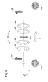
- FIG. 4 shows, in a schematic illustration, an exemplary embodiment in which a polarization-influencing optical arrangement 400 according to the invention comprises four polarization-influencing optical elements 401 - 404 , of which each, as described above, is linearly birefringent and embodied with a local variation of the fast axis of the birefringence.
- a lambda/4 plate 410 is provided upstream of the arrangement 400 in the light propagation direction (denoted by the arrow “L”) and a 45° rotator 420 is provided downstream of the arrangement 400 in the light propagation direction.
- the lambda/4 plate 410 can be made in any way from a suitable optically uniaxial crystal material such as e.g.
- the 45° rotator 420 can, in order to provide the desired polarization rotation about an angle of 45°, for example be made of optically active crystalline quartz with an alignment of the optical crystal axis parallel to the light propagation direction and with a suitable thickness.
- the above-described arrangement of the individual components leads to an initially constant linear input polarization distribution P 41 being converted into a polarization distribution P 42 with constant circular polarization as a result of the lambda/4 plate 410 .
- the individual polarization-influencing optical elements 401 - 404 of the arrangement 400 each have a radial distribution of the fast axis of the birefringence, which leads to a polarization distribution P 43 being obtained after passing through the arrangement 400 , which polarization distribution still is rotated about an angle of 45° relative to the ultimately desired tangential polarization distribution P 44 , and so the ultimately desired tangential polarization distribution P 44 is only produced by the 45° rotator 420 .
- the distribution of the fast axis of the birefringence in the elements 401 - 404 respectively is a radial distribution results in the fact that (unlike in the case of, for example, the distribution of the fast axis of the birefringence in example of FIG. 1 ) the relevant spatial distribution of the fast axis of the birefringence can also be generated by external pressure (e.g. by using piezoelectric elements).
- external pressure e.g. by using piezoelectric elements
- FIG. 5 shows, in a schematic illustration, a further embodiment of the invention.
- the latter distinguishes itself from the one in FIG. 4 in particular by virtue of the fact that a 90° rotator 530 is provided as a further component, wherein this 90° rotator 530 may, in particular, (without the invention being restricted thereto) be arranged between successive polarization-influencing optical elements 502 , 503 of the polarization-influencing optical arrangement 500 .
- both the 90° rotator 530 and the components present analogously to FIG. 4 i.e. the lambda/4 plate 510 and the 45° rotator 520
- can, in accordance with FIG. 5 be moved respectively independently of one another between a position outside of the beam path and position within the optical beam path.
- a switch can, as a result of this, more particularly occur to the effect that the ultimately generated output polarization distribution is not a tangential polarization distribution, but once again a constant linear polarization distribution P 52 , namely by virtue of only the 90° rotator 530 being placed in the optical beam path.
- the birefringence effect of the elements 501 , 502 situated upstream of the 90° rotator 530 in the light propagation direction is completely compensated for by the elements 503 and 504 situated downstream of the 90° rotator 530 in the light propagation direction (under the assumption of the overall birefringence contributions of, on the one hand, the elements 501 , 502 corresponding to, on the other hand, the contributions of the elements 503 , 504 in terms of the absolute value) such that, ultimately, the constant linear polarization distribution P 52 , corresponding to the original polarization distribution P 51 , is obtained.
Landscapes
- Physics & Mathematics (AREA)
- General Physics & Mathematics (AREA)
- Optics & Photonics (AREA)
- Health & Medical Sciences (AREA)
- Engineering & Computer Science (AREA)
- Environmental & Geological Engineering (AREA)
- Epidemiology (AREA)
- Public Health (AREA)
- Exposure Of Semiconductors, Excluding Electron Or Ion Beam Exposure (AREA)
- Polarising Elements (AREA)
- Exposure And Positioning Against Photoresist Photosensitive Materials (AREA)
Priority Applications (1)
| Application Number | Priority Date | Filing Date | Title |
|---|---|---|---|
| US14/501,770 US9588433B2 (en) | 2012-04-17 | 2014-09-30 | Optical system, in particular of a microlithographic projection exposure apparatus |
Applications Claiming Priority (6)
| Application Number | Priority Date | Filing Date | Title |
|---|---|---|---|
| US201261625171P | 2012-04-17 | 2012-04-17 | |
| DE102012206287A DE102012206287A1 (de) | 2012-04-17 | 2012-04-17 | Optisches System, insbesondere einer mikrolithographischen Projektionsbelichtungsanlage |
| DE102012206287 | 2012-04-17 | ||
| DE102012206287.4 | 2012-04-17 | ||
| PCT/EP2013/057329 WO2013156335A1 (en) | 2012-04-17 | 2013-04-08 | Optical system, in particular of a microlithographic projection exposure apparatus |
| US14/501,770 US9588433B2 (en) | 2012-04-17 | 2014-09-30 | Optical system, in particular of a microlithographic projection exposure apparatus |
Related Parent Applications (1)
| Application Number | Title | Priority Date | Filing Date |
|---|---|---|---|
| PCT/EP2013/057329 Continuation WO2013156335A1 (en) | 2012-04-17 | 2013-04-08 | Optical system, in particular of a microlithographic projection exposure apparatus |
Publications (2)
| Publication Number | Publication Date |
|---|---|
| US20150062551A1 US20150062551A1 (en) | 2015-03-05 |
| US9588433B2 true US9588433B2 (en) | 2017-03-07 |
Family
ID=49232264
Family Applications (1)
| Application Number | Title | Priority Date | Filing Date |
|---|---|---|---|
| US14/501,770 Expired - Fee Related US9588433B2 (en) | 2012-04-17 | 2014-09-30 | Optical system, in particular of a microlithographic projection exposure apparatus |
Country Status (4)
| Country | Link |
|---|---|
| US (1) | US9588433B2 (enExample) |
| JP (1) | JP2015515142A (enExample) |
| DE (1) | DE102012206287A1 (enExample) |
| WO (1) | WO2013156335A1 (enExample) |
Citations (19)
| Publication number | Priority date | Publication date | Assignee | Title |
|---|---|---|---|---|
| WO2003054590A1 (en) | 2001-12-10 | 2003-07-03 | Nikon Corporation | Fluoride crystal material for optical device used for photolithographic apparatus and its manufacturing method |
| WO2003077011A1 (en) | 2002-03-14 | 2003-09-18 | Carl Zeiss Smt Ag | Optical system with birefringent optical elements |
| US20040036971A1 (en) | 2002-08-22 | 2004-02-26 | Mcguire James P. | Methods for reducing polarization aberration in optical systems |
| WO2005026822A2 (en) | 2003-09-15 | 2005-03-24 | Carl Zeiss Smt Ag | Fly's eye condenser and illumination system therewith |
| WO2005026843A2 (en) | 2003-09-12 | 2005-03-24 | Carl Zeiss Smt Ag | Illumination system for a microlithography projection exposure installation |
| WO2005031467A2 (en) | 2003-09-26 | 2005-04-07 | Carl Zeiss Smt Ag | Microlithographic projection exposure |
| US20050146704A1 (en) | 2003-09-26 | 2005-07-07 | Carl Zeiss Smt Ag | Microlithographic exposure method as well as a projection exposure system for carrying out the method |
| WO2005069081A2 (en) | 2004-01-16 | 2005-07-28 | Carl Zeiss Smt Ag | Polarization-modulating optical element |
| US20060055909A1 (en) | 2004-07-29 | 2006-03-16 | Carl Zeiss Smt Ag | Illumination system for a microlithographic projection exposure apparatus |
| CA2521203A1 (en) | 2004-09-27 | 2006-03-27 | Her Majesty The Queen In Right Of Canada, As Represented By The Minister Of Industry Through The Communications Research Centre Canada | An optical fiber/waveguide polarizer and a method of fabrication |
| US20070115551A1 (en) | 2005-04-01 | 2007-05-24 | Alexis Spilman | Space-variant waveplate for polarization conversion, methods and applications |
| US20090237909A1 (en) | 2008-03-18 | 2009-09-24 | Advanced Mask Inspection Technology, Inc. | Light polarization control using serial combination of surface-segmented half wavelength plates |
| US20110149261A1 (en) | 2009-12-22 | 2011-06-23 | Carl Zeiss Smt Gmbh | Optical system, in particular of a microlithographic projection exposure apparatus |
| EP1720199B1 (en) | 2004-01-27 | 2011-12-07 | Nikon Corporation | Optical system, exposure system, and exposure method |
| DE102012206159A1 (de) | 2012-04-16 | 2013-06-20 | Carl Zeiss Smt Gmbh | Polarisationsbeeinflussende optische Anordnung |
| WO2013104477A1 (en) | 2012-01-12 | 2013-07-18 | Carl Zeiss Smt Gmbh | Optical system for a microlithographic projection exposure apparatus and microlithographic exposure method |
| WO2013123973A1 (en) | 2012-02-21 | 2013-08-29 | Carl Zeiss Sms Ltd. | Method and apparatus for compensating at least one defect of an optical system |
| WO2013143803A1 (en) | 2012-03-29 | 2013-10-03 | Carl Zeiss Smt Gmbh | Optical system of a microlithographic projection exposure apparatus |
| WO2013143594A1 (en) | 2012-03-29 | 2013-10-03 | Carl Zeiss Smt Gmbh | Apparatus and method for compensating a defect of a channel of a microlithographic projection exposure system |
-
2012
- 2012-04-17 DE DE102012206287A patent/DE102012206287A1/de not_active Withdrawn
-
2013
- 2013-04-08 WO PCT/EP2013/057329 patent/WO2013156335A1/en not_active Ceased
- 2013-04-08 JP JP2015506176A patent/JP2015515142A/ja active Pending
-
2014
- 2014-09-30 US US14/501,770 patent/US9588433B2/en not_active Expired - Fee Related
Patent Citations (37)
| Publication number | Priority date | Publication date | Assignee | Title |
|---|---|---|---|---|
| US20040223212A1 (en) | 2001-12-10 | 2004-11-11 | Nikon Corporation | Fluoride crystal material for optical element to be used for photolithography apparatus and method for producing the same |
| WO2003054590A1 (en) | 2001-12-10 | 2003-07-03 | Nikon Corporation | Fluoride crystal material for optical device used for photolithographic apparatus and its manufacturing method |
| WO2003077011A1 (en) | 2002-03-14 | 2003-09-18 | Carl Zeiss Smt Ag | Optical system with birefringent optical elements |
| JP2005535939A (ja) | 2002-08-22 | 2005-11-24 | オプティカル リサーチ アソシエイツ | 光学系の偏光収差を低減する構造および方法 |
| US20040036971A1 (en) | 2002-08-22 | 2004-02-26 | Mcguire James P. | Methods for reducing polarization aberration in optical systems |
| US20040036961A1 (en) | 2002-08-22 | 2004-02-26 | Mcguire James P. | Structures and methods for reducing polarization aberration in optical systems |
| WO2004019077A2 (en) | 2002-08-22 | 2004-03-04 | Optical Research Associates | Structures and methods for reducing retardance |
| WO2005026843A2 (en) | 2003-09-12 | 2005-03-24 | Carl Zeiss Smt Ag | Illumination system for a microlithography projection exposure installation |
| WO2005026822A2 (en) | 2003-09-15 | 2005-03-24 | Carl Zeiss Smt Ag | Fly's eye condenser and illumination system therewith |
| JP2007506262A (ja) | 2003-09-15 | 2007-03-15 | カール・ツァイス・エスエムティー・アーゲー | フライアイコンデンサ及びそれを用いた照明系 |
| US20060221453A1 (en) | 2003-09-15 | 2006-10-05 | Carl Zeiss Smt Ag | Fly's eye condenser and illumination system therewith |
| EP1668420A2 (en) | 2003-09-26 | 2006-06-14 | Carl Zeiss SMT AG | Microlithographic illumination method as well as a projection illumination system for carrying out the method |
| US20110069296A1 (en) | 2003-09-26 | 2011-03-24 | Carl Zeiss Smt Ag | Microlithographic exposure method as well as a projection exposure system for carrying out the method |
| US20050146704A1 (en) | 2003-09-26 | 2005-07-07 | Carl Zeiss Smt Ag | Microlithographic exposure method as well as a projection exposure system for carrying out the method |
| WO2005031467A2 (en) | 2003-09-26 | 2005-04-07 | Carl Zeiss Smt Ag | Microlithographic projection exposure |
| JP2007515768A (ja) | 2003-09-26 | 2007-06-14 | カール・ツァイス・エスエムティー・アーゲー | マイクロリソグラフィ照明方法及びその方法を実行するための投影照明系 |
| US20090040496A1 (en) | 2003-09-26 | 2009-02-12 | Carl Zeiss | Microlithographic exposure method as well as a projection exposure system for carrying out the method |
| WO2005069081A2 (en) | 2004-01-16 | 2005-07-28 | Carl Zeiss Smt Ag | Polarization-modulating optical element |
| EP1720199B1 (en) | 2004-01-27 | 2011-12-07 | Nikon Corporation | Optical system, exposure system, and exposure method |
| US20060055909A1 (en) | 2004-07-29 | 2006-03-16 | Carl Zeiss Smt Ag | Illumination system for a microlithographic projection exposure apparatus |
| CA2521203A1 (en) | 2004-09-27 | 2006-03-27 | Her Majesty The Queen In Right Of Canada, As Represented By The Minister Of Industry Through The Communications Research Centre Canada | An optical fiber/waveguide polarizer and a method of fabrication |
| US20060067618A1 (en) | 2004-09-27 | 2006-03-30 | Hill Kenneth O | Optical fiber/waveguide polarizer and method of fabrication |
| US20070115551A1 (en) | 2005-04-01 | 2007-05-24 | Alexis Spilman | Space-variant waveplate for polarization conversion, methods and applications |
| US20090237909A1 (en) | 2008-03-18 | 2009-09-24 | Advanced Mask Inspection Technology, Inc. | Light polarization control using serial combination of surface-segmented half wavelength plates |
| DE102009055184B4 (de) | 2009-12-22 | 2011-11-10 | Carl Zeiss Smt Gmbh | Optisches System, insbesondere einer mikrolithographischen Projektionsbelichtungsanlage |
| US20110149261A1 (en) | 2009-12-22 | 2011-06-23 | Carl Zeiss Smt Gmbh | Optical system, in particular of a microlithographic projection exposure apparatus |
| WO2013104477A1 (en) | 2012-01-12 | 2013-07-18 | Carl Zeiss Smt Gmbh | Optical system for a microlithographic projection exposure apparatus and microlithographic exposure method |
| JP2015509285A (ja) | 2012-01-12 | 2015-03-26 | カール・ツァイス・エスエムティー・ゲーエムベーハー | マイクロリソグラフィ投影露光装置のための光学系及びマイクロリソグラフィ露光方法 |
| US20140285788A1 (en) | 2012-01-12 | 2014-09-25 | Carl Zeiss Smt Gmbh | Optical system for a microlithographic projection exposure apparatus and microlithographic exposure method |
| US20140347646A1 (en) | 2012-02-21 | 2014-11-27 | Carl Zeiss Sms Ltd. | Method and apparatus for compensating at least one defect of an optical system |
| JP2015509662A (ja) | 2012-02-21 | 2015-03-30 | カール ツァイス エスエムエス リミテッド | 光学系の少なくとも1つの欠陥を補償する方法及び装置 |
| WO2013123973A1 (en) | 2012-02-21 | 2013-08-29 | Carl Zeiss Sms Ltd. | Method and apparatus for compensating at least one defect of an optical system |
| WO2013143803A1 (en) | 2012-03-29 | 2013-10-03 | Carl Zeiss Smt Gmbh | Optical system of a microlithographic projection exposure apparatus |
| US20150017589A1 (en) | 2012-03-29 | 2015-01-15 | Carl Zeiss Smt Gmbh | Apparatus and method for compensating a defect of a channel of a microlithographic projection exposure system |
| WO2013143594A1 (en) | 2012-03-29 | 2013-10-03 | Carl Zeiss Smt Gmbh | Apparatus and method for compensating a defect of a channel of a microlithographic projection exposure system |
| JP2015513223A (ja) | 2012-03-29 | 2015-04-30 | カール・ツァイス・エスエムティー・ゲーエムベーハー | マイクロリソグラフィ投影露光系のチャネルの欠陥を補償するための装置及び方法 |
| DE102012206159A1 (de) | 2012-04-16 | 2013-06-20 | Carl Zeiss Smt Gmbh | Polarisationsbeeinflussende optische Anordnung |
Non-Patent Citations (6)
| Title |
|---|
| Beresna, M. et al.: "Radially polarized optical vortex converter created by femtosecond laser nanostructuring of glass", Applied Physics Letter vol. 98, pp. 201101-1 to 201101-3 (2011). |
| German Office Action, with translation thereof, for DE Appl No. 10 2012 206 287.4, dated Dec. 12, 2012. |
| International Preliminary Report on Patentability for corresponding PCT Appl No. PCT/EP2013/057329, dated Oct. 30, 2014. |
| International Search Report and Written Opinion for corresponding PCT Appl No. PCT/EP2013/057329, dated Aug. 30, 2013. |
| Japanese Office Action, with English translation thereof for JP Appl. No. 2015-506176, dated Nov. 4, 2016, 17 pages. |
| Sudrie, L. et al.: "Study of damage in fused silica induced by ultra-short IR laser pulses", Optics Communications vol. 191, pp. 333-339 (2001). |
Also Published As
| Publication number | Publication date |
|---|---|
| WO2013156335A1 (en) | 2013-10-24 |
| US20150062551A1 (en) | 2015-03-05 |
| JP2015515142A (ja) | 2015-05-21 |
| DE102012206287A1 (de) | 2013-10-17 |
Similar Documents
| Publication | Publication Date | Title |
|---|---|---|
| KR101491229B1 (ko) | 마이크로리소그래픽 투영 노광 장치의 광학 시스템 | |
| JP5529922B2 (ja) | マイクロリソグラフィ投影露光装置の照明システム | |
| US8035803B2 (en) | Subsystem of an illumination system of a microlithographic projection exposure apparatus | |
| US8891060B2 (en) | Optical system, in particular of a microlithographic projection exposure apparatus | |
| US9411245B2 (en) | Polarization-influencing optical arrangement, in particular in a microlithographic projection exposure apparatus | |
| US20110194093A1 (en) | Polarization-influencing optical arrangement and an optical system of a microlithographic projection exposure apparatus | |
| US9182677B2 (en) | Optical system of a microlithographic projection exposure apparatus | |
| US8081293B2 (en) | Illumination system of a microlithographic projection exposure apparatus | |
| US9588433B2 (en) | Optical system, in particular of a microlithographic projection exposure apparatus | |
| KR20100106971A (ko) | 마이크로리소그래픽 투사 노출 장치의 조명 시스템 | |
| WO2014023619A1 (en) | Microlithographic exposure method, and microlithographic projection exposure apparatus | |
| US9405202B2 (en) | Optical system of a microlithographic projection exposure apparatus | |
| JP6140290B2 (ja) | マイクロリソグラフィー投影露光装置用光学システム及びマイクロリソグラフィー露光方法 | |
| JP5861897B2 (ja) | マイクロリソグラフィ投影露光装置のための光学系 | |
| US8922753B2 (en) | Optical system for a microlithographic projection exposure apparatus | |
| US9140994B2 (en) | Method for adjusting an optical system of a microlithographic projection exposure apparatus | |
| WO2013013894A1 (en) | Microlithographic exposure method |
Legal Events
| Date | Code | Title | Description |
|---|---|---|---|
| AS | Assignment |
Owner name: CARL ZEISS SMT GMBH, GERMANY Free format text: ASSIGNMENT OF ASSIGNORS INTEREST;ASSIGNOR:SAENGER, INGO;REEL/FRAME:033927/0243 Effective date: 20141008 |
|
| FEPP | Fee payment procedure |
Free format text: PAYOR NUMBER ASSIGNED (ORIGINAL EVENT CODE: ASPN); ENTITY STATUS OF PATENT OWNER: LARGE ENTITY |
|
| STCF | Information on status: patent grant |
Free format text: PATENTED CASE |
|
| MAFP | Maintenance fee payment |
Free format text: PAYMENT OF MAINTENANCE FEE, 4TH YEAR, LARGE ENTITY (ORIGINAL EVENT CODE: M1551); ENTITY STATUS OF PATENT OWNER: LARGE ENTITY Year of fee payment: 4 |
|
| FEPP | Fee payment procedure |
Free format text: MAINTENANCE FEE REMINDER MAILED (ORIGINAL EVENT CODE: REM.); ENTITY STATUS OF PATENT OWNER: LARGE ENTITY |
|
| LAPS | Lapse for failure to pay maintenance fees |
Free format text: PATENT EXPIRED FOR FAILURE TO PAY MAINTENANCE FEES (ORIGINAL EVENT CODE: EXP.); ENTITY STATUS OF PATENT OWNER: LARGE ENTITY |
|
| STCH | Information on status: patent discontinuation |
Free format text: PATENT EXPIRED DUE TO NONPAYMENT OF MAINTENANCE FEES UNDER 37 CFR 1.362 |
|
| FP | Lapsed due to failure to pay maintenance fee |
Effective date: 20250307 |