US9551563B2 - Multi-axis differential interferometer - Google Patents
Multi-axis differential interferometer Download PDFInfo
- Publication number
- US9551563B2 US9551563B2 US14/431,765 US201314431765A US9551563B2 US 9551563 B2 US9551563 B2 US 9551563B2 US 201314431765 A US201314431765 A US 201314431765A US 9551563 B2 US9551563 B2 US 9551563B2
- Authority
- US
- United States
- Prior art keywords
- optical module
- optical
- differential interferometer
- measurement
- interferometer
- Prior art date
- Legal status (The legal status is an assumption and is not a legal conclusion. Google has not performed a legal analysis and makes no representation as to the accuracy of the status listed.)
- Active
Links
Images


Classifications
-
- G—PHYSICS
- G01—MEASURING; TESTING
- G01B—MEASURING LENGTH, THICKNESS OR SIMILAR LINEAR DIMENSIONS; MEASURING ANGLES; MEASURING AREAS; MEASURING IRREGULARITIES OF SURFACES OR CONTOURS
- G01B9/00—Measuring instruments characterised by the use of optical techniques
- G01B9/02—Interferometers
- G01B9/02015—Interferometers characterised by the beam path configuration
-
- G—PHYSICS
- G01—MEASURING; TESTING
- G01B—MEASURING LENGTH, THICKNESS OR SIMILAR LINEAR DIMENSIONS; MEASURING ANGLES; MEASURING AREAS; MEASURING IRREGULARITIES OF SURFACES OR CONTOURS
- G01B11/00—Measuring arrangements characterised by the use of optical techniques
- G01B11/14—Measuring arrangements characterised by the use of optical techniques for measuring distance or clearance between spaced objects or spaced apertures
-
- G—PHYSICS
- G01—MEASURING; TESTING
- G01B—MEASURING LENGTH, THICKNESS OR SIMILAR LINEAR DIMENSIONS; MEASURING ANGLES; MEASURING AREAS; MEASURING IRREGULARITIES OF SURFACES OR CONTOURS
- G01B11/00—Measuring arrangements characterised by the use of optical techniques
- G01B11/26—Measuring arrangements characterised by the use of optical techniques for measuring angles or tapers; for testing the alignment of axes
-
- G—PHYSICS
- G01—MEASURING; TESTING
- G01B—MEASURING LENGTH, THICKNESS OR SIMILAR LINEAR DIMENSIONS; MEASURING ANGLES; MEASURING AREAS; MEASURING IRREGULARITIES OF SURFACES OR CONTOURS
- G01B9/00—Measuring instruments characterised by the use of optical techniques
- G01B9/02—Interferometers
- G01B9/02015—Interferometers characterised by the beam path configuration
- G01B9/02017—Interferometers characterised by the beam path configuration with multiple interactions between the target object and light beams, e.g. beam reflections occurring from different locations
- G01B9/02021—Interferometers characterised by the beam path configuration with multiple interactions between the target object and light beams, e.g. beam reflections occurring from different locations contacting different faces of object, e.g. opposite faces
-
- G—PHYSICS
- G01—MEASURING; TESTING
- G01B—MEASURING LENGTH, THICKNESS OR SIMILAR LINEAR DIMENSIONS; MEASURING ANGLES; MEASURING AREAS; MEASURING IRREGULARITIES OF SURFACES OR CONTOURS
- G01B9/00—Measuring instruments characterised by the use of optical techniques
- G01B9/02—Interferometers
- G01B9/02015—Interferometers characterised by the beam path configuration
- G01B9/02027—Two or more interferometric channels or interferometers
-
- G—PHYSICS
- G01—MEASURING; TESTING
- G01B—MEASURING LENGTH, THICKNESS OR SIMILAR LINEAR DIMENSIONS; MEASURING ANGLES; MEASURING AREAS; MEASURING IRREGULARITIES OF SURFACES OR CONTOURS
- G01B9/00—Measuring instruments characterised by the use of optical techniques
- G01B9/02—Interferometers
- G01B9/02049—Interferometers characterised by particular mechanical design details
- G01B9/02051—Integrated design, e.g. on-chip or monolithic
-
- G—PHYSICS
- G03—PHOTOGRAPHY; CINEMATOGRAPHY; ANALOGOUS TECHNIQUES USING WAVES OTHER THAN OPTICAL WAVES; ELECTROGRAPHY; HOLOGRAPHY
- G03F—PHOTOMECHANICAL PRODUCTION OF TEXTURED OR PATTERNED SURFACES, e.g. FOR PRINTING, FOR PROCESSING OF SEMICONDUCTOR DEVICES; MATERIALS THEREFOR; ORIGINALS THEREFOR; APPARATUS SPECIALLY ADAPTED THEREFOR
- G03F7/00—Photomechanical, e.g. photolithographic, production of textured or patterned surfaces, e.g. printing surfaces; Materials therefor, e.g. comprising photoresists; Apparatus specially adapted therefor
- G03F7/70—Microphotolithographic exposure; Apparatus therefor
- G03F7/70691—Handling of masks or workpieces
- G03F7/70775—Position control, e.g. interferometers or encoders for determining the stage position
-
- G—PHYSICS
- G03—PHOTOGRAPHY; CINEMATOGRAPHY; ANALOGOUS TECHNIQUES USING WAVES OTHER THAN OPTICAL WAVES; ELECTROGRAPHY; HOLOGRAPHY
- G03F—PHOTOMECHANICAL PRODUCTION OF TEXTURED OR PATTERNED SURFACES, e.g. FOR PRINTING, FOR PROCESSING OF SEMICONDUCTOR DEVICES; MATERIALS THEREFOR; ORIGINALS THEREFOR; APPARATUS SPECIALLY ADAPTED THEREFOR
- G03F7/00—Photomechanical, e.g. photolithographic, production of textured or patterned surfaces, e.g. printing surfaces; Materials therefor, e.g. comprising photoresists; Apparatus specially adapted therefor
- G03F7/70—Microphotolithographic exposure; Apparatus therefor
- G03F7/708—Construction of apparatus, e.g. environment aspects, hygiene aspects or materials
- G03F7/70808—Construction details, e.g. housing, load-lock, seals or windows for passing light in or out of apparatus
- G03F7/70833—Mounting of optical systems, e.g. mounting of illumination system, projection system or stage systems on base-plate or ground
-
- G—PHYSICS
- G03—PHOTOGRAPHY; CINEMATOGRAPHY; ANALOGOUS TECHNIQUES USING WAVES OTHER THAN OPTICAL WAVES; ELECTROGRAPHY; HOLOGRAPHY
- G03F—PHOTOMECHANICAL PRODUCTION OF TEXTURED OR PATTERNED SURFACES, e.g. FOR PRINTING, FOR PROCESSING OF SEMICONDUCTOR DEVICES; MATERIALS THEREFOR; ORIGINALS THEREFOR; APPARATUS SPECIALLY ADAPTED THEREFOR
- G03F7/00—Photomechanical, e.g. photolithographic, production of textured or patterned surfaces, e.g. printing surfaces; Materials therefor, e.g. comprising photoresists; Apparatus specially adapted therefor
- G03F7/70—Microphotolithographic exposure; Apparatus therefor
- G03F7/708—Construction of apparatus, e.g. environment aspects, hygiene aspects or materials
- G03F7/7085—Detection arrangement, e.g. detectors of apparatus alignment possibly mounted on wafers, exposure dose, photo-cleaning flux, stray light, thermal load
-
- H—ELECTRICITY
- H01—ELECTRIC ELEMENTS
- H01J—ELECTRIC DISCHARGE TUBES OR DISCHARGE LAMPS
- H01J37/00—Discharge tubes with provision for introducing objects or material to be exposed to the discharge, e.g. for the purpose of examination or processing thereof
- H01J37/30—Electron-beam or ion-beam tubes for localised treatment of objects
- H01J37/317—Electron-beam or ion-beam tubes for localised treatment of objects for changing properties of the objects or for applying thin layers thereon, e.g. for ion implantation
- H01J37/3174—Particle-beam lithography, e.g. electron beam lithography
-
- Y—GENERAL TAGGING OF NEW TECHNOLOGICAL DEVELOPMENTS; GENERAL TAGGING OF CROSS-SECTIONAL TECHNOLOGIES SPANNING OVER SEVERAL SECTIONS OF THE IPC; TECHNICAL SUBJECTS COVERED BY FORMER USPC CROSS-REFERENCE ART COLLECTIONS [XRACs] AND DIGESTS
- Y10—TECHNICAL SUBJECTS COVERED BY FORMER USPC
- Y10T—TECHNICAL SUBJECTS COVERED BY FORMER US CLASSIFICATION
- Y10T156/00—Adhesive bonding and miscellaneous chemical manufacture
- Y10T156/10—Methods of surface bonding and/or assembly therefor
Definitions
- the invention relates to a multi-axis differential interferometer for measuring a displacement and/or rotation between a first reflective surface and a second reflective surface.
- the invention further relates to a lithography system comprising such differential interferometer, and to a method for assembling such differential interferometer.
- Interferometers for measuring a stage position in an e-beam lithography tool are known. Paul. G. Harris et al. discloses an e-beam tool comprising an interferometer for measuring its stage position.
- the differential interferometer comprises a signal detection unit having a bi-refringent wedge for receiving a measurement beam and a reference beam that run in parallel.
- the wedge creates an angular deviation between the beams, and the beams then pass through a Polaroid aligned at 45° to make them interfere.
- the resultant interference pattern is a linear array of fringes. These fringes are aligned with an integrated linear photodiode array, called an electrograting.
- the electrograting produces four electrical signals of relative phase 0°, 90°, 180°, and 270°.
- the gain matching of the electrograting allows the differential amplifier to remove common mode intensity changes on the signals due to an intensity change of the laser, for example, which results in a good measurement performance.
- the interferometer is only capable of measuring a relative position of the stage.
- the interferometer is difficult to assemble, as the optical parts in the detector must be positioned and configured carefully.
- the present invention provides a multi-axis differential interferometer for measuring a displacement and/or rotation between a first reflective surface and a second reflective surface, wherein said measuring is carried out using at least two pairs of beams, wherein each pair is formed by a measurement beam to be emitted onto a first one of said reflective surfaces, and a reference beam to be emitted onto another one of said reflective surfaces, said interferometer comprising: a first optical module and a second optical module, wherein each optical module is configured for receiving a respective coherent beam and for creating one of said pairs therefrom.
- the present invention provides a method of assembling a multi-axis differential interferometer, preferably a differential interferometer as described above, the method comprising the steps of:
- said method further comprising the steps of:
- a multi-axis differential interferometer is obtained by using two pairs of measurement-reference beams. Furthermore, each of these pairs of such beams is created in a separated optical module, which thereby increases the modularity of said interferometer significantly, and also renders the manufacturability relatively easy.
- the invention renders it possible to use very small optical elements inside the optical elements as each optical element only needs to create and handle one measurement beam and one reference beam.
- Non-prepublished international patent application no PCT/NL2012/050209 by Applicant discloses a differential interferometer module which generates signals from which a relative displacement along one axis, e.g. the X-axis, and a rotation around two other axes, e.g. around Rz and Ry, may be derived.
- This differential interferometer module comprises a beam source adapted for providing three coherent beams, a beam splitter unit adapted for splitting said three beams into respective pairs of measurement beams and associated reference beams, wherein the three measurement beams are incident on a first reflective surface, and wherein the three reference beams are incident on a second reflective surface moveable with respect to said first reflective surface, at least one beam combiner for combining each reflected measurement beam with its associated reflected reference beam to a combined beam, and three beam receivers, wherein each combined beam is projected onto a corresponding detector.
- a beam source adapted for providing three coherent beams
- a beam splitter unit adapted for splitting said three beams into respective pairs of measurement beams and associated reference beams, wherein the three measurement beams are incident on a first reflective surface, and wherein the three reference beams are incident on a second reflective surface moveable with respect to said first reflective surface
- at least one beam combiner for combining each reflected measurement beam with its associated reflected reference beam to a combined beam
- three beam receivers
- the known differential interferometer module provides a compact differential interferometer module.
- a drawback of the known module is that the dimensions of the optical elements, in particular of the beam splitter unit, must be relatively large in order to provide sufficient surface area for splitting the three coherent beams into corresponding measurement and reference beams. The cost of such large elements forms a substantial part of the cost of the module.
- said optical modules have a similar configuration. Similar configurations of the optical modules leads to easier manufacturability.
- said optical modules are arranged to form a side-by-side stack. The advantage is that in such configuration all measurement beams may be directed to the first one of said reflective surfaces, and likewise, all reference beams may be directed to the second one of said reflective surfaces, which results in a convenient compact solution. Side-by-side stackable optical modules having a similar configuration render the assembly of said interferometer even easier.
- said three optical modules are arranged to emit said measurement beams substantially in parallel. With this configuration it is possible to determine a displacement and/or rotation of the reference surface relative to the measurement surface in three degrees of freedom.
- the optical modules are arranged in a stack.
- the multi-axis differential interferometer thus forms a differential interferometer stack module.
- each optical module only has to be of a dimension sufficient for splitting a single coherent beam into a corresponding measurement and reference beam
- the beam splitter may be much smaller than when it is used to split multiple coherent beams into measurement and reference beams.
- any other optical elements in an optical module may also be dimensioned for a single beam.
- each of said interferometer optical modules comprises a housing forming an outer surface of said interferometer optical module.
- Each interferometer optical module thus forms a self contained module.
- a separate interferometer optical module which is adapted for emitting a single measurement beam and a single corresponding reference beam is much more easily produced, in particular more easily produced than complex differential interferometers which emit two or more measurement beams and corresponding reference beams.
- the housing of an interferometer optical module completely envelops said element, thus protecting the inside of the element from dust and damage due to handling.
- said housing of at least the second optical module comprises at least three sides of a rectangular cuboid, such that the first and second planar sides are two of said sides of said rectangular cuboid.
- the second interferometer optical module comprises two parallel sides for stacking against corresponding parallel sides of the neighboring first and third interferometer optical modules, preferably wherein said two parallel sides are planar and/or substantially parallel to a direction in which said second interferometer optical module is to emit its reference beam.
- sides of neighboring optical modules comprise protrusions and corresponding cut-outs to substantially form fit with each other when the optical modules are arranged in a stack.
- the interferometer optical modules are automatically substantially aligned with each other when stacked.
- the housing of said first interferometer optical module has a substantially planar side facing a first substantially planar side of said housing of said second interferometer optical module
- said housing of said second interferometer optical module has a second substantially planar side opposite from said first substantially planar side and facing a planar side of said housing of said third interferometer optical module.
- said housings of said interferometer optical modules have substantially equal outer dimensions, and/or shapes. During assembly of the differential interferometer, the order in which the optical modules are stacked is thus not determined by the shape or dimensions of the housings of said optical modules.
- said housings of said optical modules each comprise a material having a low thermal expansion coefficient, such as ZerodurTM.
- a low thermal expansion coefficient material is meant in particular material having a thermal expansion coefficient which is less than or substantially equal to a thermal expansion coefficient of the optics used in said optical module.
- said optical modules are attached to each other.
- said differential interferometer further comprises a first alignment body arranged between said first optical module and said second optical module.
- the optical modules may thus be easily and accurately aligned relative to each other such that irregularities in the outer surfaces of the housings of the optical modules may be compensated for, and/or slight misalignments of the optics of an optical module relative to its housing are compensated for.
- said measuring is carried out using three pairs of beams, wherein each pair is formed by a measurement beam and a reference beam.
- said interferometer further comprises a third optical module configured for receiving a further respective coherent beam and for creating a further pair of beams being formed by a further measurement beam and a further reference beam.
- said differential interferometer further comprises a second alignment body arranged between said second optical module and said third optical module.
- the optical modules may thus be easily and accurately aligned relative to each other such that irregularities in the outer surfaces of the housings of the optical modules may be compensated for, and/or slight misalignments of the optics of an optical module relative to its housing are compensated for.
- said three optical modules ( 20 , 40 , 60 ) are arranged to emit said measurement beams (Mb) non-coplanarly. This arrangement opens up the possibility to measure a further rotation, next to the position and rotation which can be measurement using at least two optical modules.
- said first alignment body comprises a body of a cured adhesive.
- said second alignment body comprises a body of cured adhesive.
- said first alignment body comprises a tapered shim.
- said second alignment body comprises a tapered shim.
- said reference beams are emitted in a configuration corresponding to said measurement beams. For instance, when the measurement beams are emitted in an “L”-configuration, in which the a first and a second of said measurement beams span a first plane, and in which said second and a third of said measurement beams span a second plane perpendicular to said first plane, the reference beams are emitted in the same configuration.
- said optical modules are arranged such that their respective reference beams are emitted substantially coplanarly.
- the differential interferometer may be of a substantially smaller dimension than a differential interferometer in which the reference beams are emitted non-coplanarly.
- the volume of space required in said lithography system for passage of the reference beams and the reference beams is reduced as well.
- the first and third optical modules are of a same, or identical, construction, and the second optical module is of a different construction.
- the difference in construction is in particular defined by the distances between the openings for emitting the reference beam and corresponding measurement beam of each optical module, e.g. this distance is equal for the identically shaped first and third optical modules, and is different, preferably less, for the second optical module.
- all optical modules have their respective openings oriented in an asymmetric manner in that each of said optical modules comprises an opening for letting through said measurement beam, and an opening for letting through said reference beam.
- said openings are arranged on a line and each arranged at different distances from a respective closest edge of the housing of said optical module along said line.
- Said first and third optical module are arranged in said differential interferometer in a same rotational orientation, and said second optical module is arranged rotated, in a plane parallel to a surface comprising said openings, 180 degrees with respect to said orientation. Said rotation is typically around an axis parallel to the direction of emission of the reference beam of the second optical module.
- each optical module comprises an opening through which to emit its measurement beam and an opening through which to emit its reference beam.
- These openings are preferably arranged on a line and each arranged at different distances from a respective closest edge of the housing of said optical module along said line. If the three optical modules were arranged in a stack in identical configurations, both the measurement beams and the reference beams would be emitted in respective measurement and reference planes.
- the second optical module is arranged between the first and third optical module in an “upside down” configuration with respect to the first and third optical modules, the optical modules are arranged for emitting the reference beams and the measurement beams non-coplanarly.
- a multi-axis differential interferometer is obtained capable of measuring a relative displacement and/or rotation between the reference surface and the measurement surface, wherein each of said optical modules is of a substantially same or identical construction. It must be noted at this stage that this embodiment relies upon the fact that for differential interferometers the measurement beam and the reference beam may be exchanged without hampering the performance of the device. Expressed differently, it is not relevant which beam is called the reference beam or the measurement beam.
- the differential interferometer is only measuring a path length difference between said beams.
- the polarizations of said first and third polarized beams are the same in this embodiment as well as said second and fourth polarized beams.
- the half-wave plate ensures that the beam polarization is rotated with 45 degrees before it reaches the second polarizing beam splitter.
- the third detector a 135 degrees rotated polarization
- the fourth detector a 45 degrees rotated polarization. Consequently, the four detectors provide four interference signals wherein each interference signal is typically a sinusoid signal shifted in phase relative to the other signals. It is thus possible to determine a direction of displacement between said measurement reflective surface and said reference reflective surface.
- the resolution of the measurement may be improved.
- the half wave plate is arranged between the polarizing beam splitter and said first polarizing beam splitter or between said non polarizing beam splitter and said second polarizing beam splitter.
- the advantage is that the first polarizing beam splitter and the second polarizing beam splitter do not have to be at a 45 degree angle to each other to provide the four different polarizations.
- the optical elements within the optical module may thus be mounted on one side of the housing, with the sides of said optical elements which are fixed to the one side of the housing substantially parallel thereto.
- the volume of the optical module is substantially smaller than if it were necessary to rotate the first polarizing beam splitter relative to the second polarizing beam splitter to obtain four different polarizations at the four detectors.
- said optical modules are arranged for emitting said reference beams substantially parallel to each other and/or for emitting said measurement beams substantially parallel to each other.
- said beam splitter and said beam combiner of an optical module are part of a group of optical elements of said optical module, and said optical elements within an optical module are bonded to each other using optical surface bonding (also known as “Ansprengen”).
- optical surface bonding also known as “Ansprengen”.
- said beam splitter and said beam combiner of an optical module are part of a group of optical elements of said optical module, and wherein said optical elements of an optical module of said optical modules are bonded together using an adhesive, preferably an optically neutral adhesive.
- each of said optical modules is arranged outside a path of said reference and/or measurement beams emitted by said other optical modules.
- the optical modules are thus clearly separate elements which do not interfere with each other.
- the second optical module comprises two parallel sides for stacking against corresponding parallel sides of the neighboring first and third optical modules, preferably wherein said two parallel sides are planar and/or substantially parallel to a direction in which said second optical module is to emit its reference beam.
- the present invention provides a lithography system comprising:
- the target carrier ( 66 ) is provided with a first reflective surface ( 21 ), and wherein the optical column ( 36 ) is provided with a second reflective surface ( 81 ), and
- the interferometer of the invention is advantageously used in a lithography system, because of its low cost and low volume.
- the present invention provides a method of assembling a differential interferometer stack module comprising the steps of
- said method further comprising the steps of:
- pre-manufactured optical modules may be accurately aligned and bonded together to form a differential interferometer stack, or differential interferometer stack module. Once the body of adhesive has cured, the bonded optical modules form a structurally robust module.
- Aligning of the first and second optical module for instance comprises emitting said reference and measurement beams from said first and second optical module onto one or more detectors for determining a position of said beams, and changing the position and/or orientation of said first optical module relative to said second optical module based on said measured beam positions.
- the third optical module is aligned with the second optical module.
- the third optical module is thus also automatically aligned with the first optical module.
- the interferometer of the invention is charatererized in that said measurement beam and said reference beam are created using a polarizing splitter and a prism, adapted to orient said beams in parallel, each optical module comprising a housing provided with a planar surface to which optical elements are mounted, and in that each of said housings is provided with a cuboid shape.
- Both the measurement beams and the reference beams are thus confined to a single plane, which allows the interferometer to be more compact than those currently known.
- This effect is further enhanced by mounting the optical elements on a planar surface and the cuboid shape, such that the optical modules can be nicely fitted side by side without any loose space being created in between them.
- the smaller size of the interferometer means that relatively small optical elements will have to be used this is actually another advantage as smaller optical elements are more economically (cheaper) manufactured than bigger ones.
- FIG. 1A shows an embodiment of a multi-axis differential interferometer (differential interferometer stack module) according to the present invention
- FIG. 1B shows an exploded view of a differential interferometer of FIG. 1A ;
- FIG. 2A shows another embodiment of a differential interferometer according to the present invention
- FIG. 2B shows an exploded view of a differential interferometer of FIG. 2A ;
- FIG. 3 shows another embodiment of a differential interferometer according to the present invention
- FIG. 4A schematically shows a cross sectional view of an optical module as may be included in a multi-axis differential interferometer (differential interferometer stack module) according to the present invention
- FIG. 4B schematically shows a cross sectional view of another embodiment of an optical module as may be included in a differential interferometer stack module according to the present invention
- FIG. 5 shows a flow chart of steps of a method for assembling a differential interferometer stack module according to the present invention
- FIGS. 6A and 6B show schematic side views of a lithography system according to the present invention.
- FIG. 6C shows a schematic side view of a further embodiment of a lithography system according to the present invention.
- FIG. 1A shows a multi-axis differential interferometer 1 according to the present invention, comprising a first optical module 20 , a second optical module 40 and a third optical module 60 .
- the optical modules are arranged for emitting three measurement beams from openings 22 , 42 and 62 , and for emitting three corresponding reference beams from openings 21 , 41 and 61 .
- As the measurement beams and the reference beams are emitted non-coplanarly it is possible to measure displacement and/or rotation between a reflective measurement surface (first reflective surface) onto which the measurement beams are emitted and a reflective reference surface (second reflective surface) onto which the reference beams are emitted (see FIG. 3 ), in three degrees of freedom.
- a single differential interferometer 1 may be used to measure a displacement along X between a measurement surface and a reference surface, as well as a rotation around an axis Rz parallel to Z or and around an axis Ry parallel to Y between said reflective surfaces.
- the optical modules 20 , 40 , 60 are substantially of a same construction.
- First optical module 20 comprises openings 21 , 22 arranged on a line at distances d 6 and d 5 respectively from the edge closest to said respective openings on said line.
- second optical module 40 comprises openings 41 , 42 arranged on a line at distances d 5 and d 6 respectively from the edge closest to said respective openings on said line
- third optical module 60 comprises openings 61 , 62 arranged on a line at distances d 6 and d 5 respectively from the edge closest to said respective openings on said line.
- the distance d 1 between openings 21 and 22 is substantially equal to the distance d 2 between openings 41 and 42 , which in turn is substantially equal to the distance d 3 between openings 61 and 62 .
- the distance d 6 between opening 21 and the closest edge of the optical module 20 along a line through opening 21 and 22 is greater than distance d 4 , which is the distance between openings 41 and 21 when projected onto a plane normal to a line intersecting the center of openings 21 and 61 .
- the height h 1 of the differential interferometer is greater than the distance d 4 , i.e. the height h 1 of the interferometer is at least partly dependent on said distance d 4 .
- the orientation of second optical module 40 in the differential interferometer 1 is flipped 180 degrees relative to the orientation of the first and third optical modules 20 , 60 .
- the optical modules 20 , 40 , 60 are arranged for emitting reference beams and corresponding reference beams non-coplanarly respectively from openings 21 , 41 , 61 and 22 , 42 , 62 . More specifically, an angle ⁇ between openings 21 , 41 and 61 for the reference beams is substantially equal to angle ⁇ between corresponding openings 22 , 42 and 62 for the measurement beams.
- the first optical module 20 is attached to the second optical module 40 by means of a body of adhesive (see FIG. 1B ), and the second optical module 20 is attached to the third optical module by means of a further body of adhesive (see FIG. 1B ), thus forming a single differential interferometer stack module.
- a body of adhesive see FIG. 1B
- a further body of adhesive see FIG. 1B
- FIG. 1B shows an exploded view of the differential interferometer stack module of FIG. 1A .
- Each of the elements 20 , 40 , 60 comprises a respective housing 23 , 43 , 63 forming an outer surface of the respective optical module.
- the housing protects the interior of each optical module 20 , 40 , 60 against dust and also the optical modules with a robust structure.
- the housings 23 , 43 , 63 each have a substantially rectangular cuboid shape, also denoted bar shape, with planar sides facilitating stacking of the elements 20 , 40 , 60 on each other. Such planar sides can be machined highly accurately to specifications.
- the second optical module comprises two parallel sides for stacking against corresponding parallel sides of the neighboring first and third optical modules, preferably wherein said two parallel sides are substantially parallel to a direction in which said second optical module is to emit its reference beam.
- sides of neighboring optical modules comprise protrusions and corresponding cut-outs to substantially form fit with each other when the optical modules are arranged in a stack.
- the housings 23 , 43 and 63 may comprise material having a low thermal expansion coefficient. Errors in measurement between the reference surface and the measurement surface due to thermal expansion of the differential interferometer 1 are thus reduced or avoided.
- An example of a low thermal expansion coefficient material is ZerodurTM.
- the housings may comprise a material having a thermal expansion coefficient which is substantially equal to a thermal expansion coefficient of the optics which are comprised within said housings.
- the housing 43 of the second optical module 40 comprises a substantially planar first side 45 for mounting to an opposing substantially planar side 25 of the housing 23 of first optical module 20 .
- the housing 43 of the second optical module 40 further comprises a substantially planar second side 46 , opposite from said first side 45 , for mounting to an opposing substantially planar side 65 of the housing 63 of the third optical module 60 .
- a body of an adhesive 80 and a further body of adhesive 81 are arranged between the planar side 25 of the first optical module 20 and the first planar side 45 of the second optical module 40 , and between the second planar side 46 of the second optical module 40 and the planar side 65 of the third optical module 60 respectively.
- the optical modules 20 , 40 , 60 may be aligned relative to each other as long as the body of adhesive 80 has not yet cured.
- the thickness of the body of adhesive 80 which determines the distance between the side 25 of the first optical module 20 and the first side 45 of the second optical module 40 , may be varied according to the requirements for alignment.
- the thickness of the further body of adhesive 81 may be varied likewise.
- the body of adhesive and/or further body of adhesive, which form alignment bodies may have a tapered shape or any other shape as required for alignment of the optical modules.
- FIG. 2A shows a second embodiment of a differential interferometer 100 according to the present invention.
- the differential interferometer 100 comprises a first optical module 120 , a second optical module 140 and a third optical module 160 .
- each of the optical modules is differential optical module adapted for emitting a measurement beam and a corresponding reference beam.
- the first optical module 120 and the third optical module 160 are of a similar or identical construction. Openings 121 , 122 of the first optical module and openings 161 , 162 of the third optical module are at distances d 1 ′ and d 3 ′ from each other respectively, which distances d 1 ′ and d 3 ′ are substantially equal.
- Second optical module 140 is of a different construction, comprising openings 141 and 142 which are spaced apart from each other by a distance d 2 ′ which is less than said distances d 1 and d 3 .
- the openings 121 , 141 and 161 through which the reference beams are to be emitted are arranged on a line such that the reference beams are emitted coplanarly.
- openings 121 and 141 are projected on a plane normal to a line through opening 121 of the first optical module 120 and opening 161 of the second optical module 160 , they coincide, i.e. in such a projection the distance between openings 121 and 141 and between openings 141 and 161 is substantially zero.
- the height h 2 of the differential interferometer is substantially less than the height h 1 of the first embodiment shown in FIG. 1A .
- a volume spanned by the reference beams and the measurement beams emitted by the differential interferometer according to this second embodiment is smaller than the volume spanned by the reference and measurement beams emitted by the interferometer according to the first embodiment.
- the space required by the beams emitted by the differential interferometer along the direction of the height h 2 is reduced as well.
- space is at a premium, and any reduction in space requirements for an interferometer and the beams emitted thereby is highly desirable.
- a disadvantage of the embodiment of FIG. 2A is that a rotation of the reference surface is no longer affecting the measurement. Rotation of the measurement surface can still be measured, albeit that such measurement then no longer occurs differentially (no common mode rejection for this rotation measurement.
- the openings 122 , 142 , 162 for the measurement beams are arranged in an “L-configuration”, as described earlier herein, such that it remains possible to measure a displacement and/or rotation between a measurement surface and a reference surface in three degrees of freedom.
- an alignment body is arranged, which is shown in FIG. 2B .
- FIG. 2B shows an exploded view of the differential interferometer of FIG. 2A .
- Each of the optical modules comprises a respective housing 123 , 143 and 163 , which protects the interior of its corresponding optical module 120 , 140 , 160 respectively from damage and dust, and which provides substantially planar surfaces which facilitate stacking of the optical modules to form a complete differential interferometer, or differential interferometer stack module.
- the optical modules are fixed relatively to each other, preferably by means of a body of adhesive as described earlier herein and shown in FIG. 1B .
- FIG. 1B shows an exploded view of the differential interferometer of FIG.
- a tapered shim 183 for instance a tapered sheet of aluminum of a ceramic material which is preferably easily machined, is arranged between the first optical module 120 and the second optical module.
- a tapered shim 183 may be used during assembly of the differential interferometer stack module for aligning the optical modules relative to each other.
- the shim may form part of an alignment body which keeps the optical modules aligned.
- FIG. 4A shows a cross-sectional view of the interior of an optical module as used in the present invention.
- the interiors of the optical modules used in a differential interferometer according to the invention are similar to each other.
- a single coherent beam b of light is emitted onto polarizing beam splitter 301 , which splits the beam b into a polarized measurement beam Mb and an associated polarized reference beam Rb.
- the measurement beam Mb passes a quarter wave plate 303 .
- the incident measurement beam is then reflected back by reflective measurement surface, or mirror, 321 , and again passes the quarter wave plate 303 .
- the reflected measurement beam is reflected by the polarizing beam splitter 301 to pass through an iris 340 .
- the part of the coherent beam that forms the reference beam Rb is reflected by prism 302 through a quarter wave plate 303 and incident on reflective reference surface, or mirror 381 .
- the reference beam Rb is then reflected back by reflective surface 381 and again passes through the same quarter wave plate 303 , after which it is reflected by prism 302 , through polarizing beam splitter 301 towards iris 304 .
- a combined beam Cb passes the iris 304 .
- a non-polarizing beam splitter 305 splits the combined beam into two, wherein the two combined beam portions into which the combined beam is split comprise both a portion of the reflected reference beam and a portion of the reflected measurement beam.
- the two beam portions in turn are split by polarizing beam splitters 306 and 307 respectively. Because a half-wave plate 320 is arranged between non-polarizing beam splitter 305 and polarizing beam splitter 307 , it is not necessary to arrange polarizing beam splitter 306 at a 45 degree angle with respect to polarizing beam splitter 307 to obtain beams with four different polarizations at detectors 308 , 309 , 310 and 311 .
- a half-wave plate 320 is provided in between non-polarizing beam splitter 305 and polarizing beam splitter 307 , such that, the beam in between these two elements gets a polarization which is rotated with 45 degrees. This means that effectively, the detectors 310 , 311 cooperating with this non-polarizing beam splitter 305 measure a 45 degree polarization and a 135 degree polarization, respectively.
- Detectors 308 , 309 , 310 and 311 convert powers of these four combined beam portions into a four respective signals, from which a direction of displacement and a magnitude of displacement may be derived using techniques which are well known within the field of differential interferometrics. Electrical signals from the detectors are transferred via wires to a connector 354 for connection with a further processing device.
- the optical module 300 comprises a housing 323 having a planar inner surface 337 to which the optical elements 301 , 302 , 303 , 305 , 306 and 307 are mounted. All of these optical elements are arranged within the housing 323 which is a substantially closed housing protecting the optical elements inside thereof against dust and handling.
- Half-wave plate 320 is mounted to non-polarizing beam splitter 305 and polarizing beam splitter 307 by means of optical surface mounting (“Ansprengen”).
- Non-polarizing beam splitter 305 is attached to polarizing beam splitter 306 using a layer of optically neutral adhesive 322 .
- FIG. 4B shows an alternative embodiment of a optical module as used in a differential interferometer according to the invention.
- Parts 400 , 402 , 403 and 440 correspond to the parts 300 , 302 , 303 and 440 of FIG. 4A .
- the embodiment of FIG. 4B is less complex than the embodiment of FIG. 4A in that the optical module 400 comprises only a single detector for measuring a power of combined beam Cb.
- the optical module 400 comprises only a single detector for measuring a power of combined beam Cb.
- the optical module 400 comprises only a single detector for measuring a power of combined beam Cb.
- the optical module 400 comprises only a single detector for measuring a power of combined beam Cb.
- the optical module 400 comprises only a single detector for measuring a power of combined beam Cb.
- the optical module 400 comprises only a single detector for measuring a power of combined beam Cb.
- the optical module 400 comprises only a single detector for measuring a power of combined beam Cb.
- the optical module 400 comprises
- FIG. 5 shows a flow chart of a method for assembling a differential interferometer stack module according to the present invention.
- step 500 at least three optical modules as described herein are provided, which are arranged in a stack in step 501 .
- a body of adhesive is applied between a side of the first optical module and a side of the second optical module facing said side of the first optical module.
- step 503 while the adhesive has not yet cured, the first optical module and the second optical module are aligned with respect to each other. This may for instance be done by having said first and second optical modules emit measurement beams and/or reference beams onto a detector for detecting a position of said beams, and adjusting the position and/or orientation of the first optical module relative to the second optical module correspondingly.
- Alignment of the optical modules may also comprise inserting one or more alignment bodies, such as shims, between the first and second optical modules for spacing these elements apart. These shims may be left in place during curing of the body of adhesive, or may be removed just before the adhesive has completely cured.
- step 504 the first and second optical modules are held in place until the body of adhesive has cured.
- step 505 which is optional, steps corresponding to steps 502 - 504 are repeated for aligning the second optical module with the third optical module. It is noted that step 505 may be performed at least partially at the same time as steps 502 - 504 , i.e. the second optical module may be aligned with the first and third optical modules at substantially the same time.
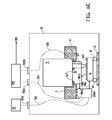
- FIG. 6A shows a lithography system according to the present invention.
- the system comprises a frame 4 , to which an optical column 36 having an optical axis 37 is mounted.
- the optical column 36 is adapted for projecting a plurality of exposure beamlets 10 onto a target 7 .
- an exposure surface of the target below the optical column may be patterned.
- the target is placed on a wafer table 6 , which in turn is placed on a chuck 66 which is moveable with respect to the optical column 36 by means of a stage 9 on which the chuck 66 is placed.
- the chuck 66 , wafer table 6 and stage 9 form a target carrier for moving the target 7 relative to the optical column 36 .
- the chuck 66 comprises a first reflective surface (or mirror) 21 , comprising a substantially planar surface at substantially the same level or height within the system as the target 7 or exposure surface thereof.
- the optical column comprises a second reflective surface (or mirror) 81 , which comprises a substantially planar surface close to the projection end of the optical column.
- the system further comprises a modular interferometer head 960 , or differential interferometer module, which is mounted to the frame 4 by means of a kinematic mount 962 , 963 , 964 .
- the modular interferometer head 960 emits reference beams Rb onto the second reflective surface 81 , and associated measurement beams Mb onto the first reflective surface 21 .
- the reference beams comprise three reference beams
- the measurement beams comprise three measurement beams
- a relative movement between the first reflective surface 81 and second reflective surface 21 is measured by evaluating interference between a reference beam and its associated measurement beam.
- the three measurement beams Mb and the three reference beams Rb originate from a laser unit 31 which supplies a beam of coherent light, and which is coupled into the interferometer module 999 via an optical fiber 92 which forms part of a beam source for the module 999 .
- FIG. 6B schematically shows the lithography system of FIG. 6A , wherein the lithography system comprises a vacuum housing 2 .
- the vacuum housing 2 Within the vacuum housing 2 , only the interferometer head 960 and its connections, and first 81 and second reflective surfaces 21 are shown, though it will be understood that the target carrier of FIG. 1A will be contained within the vacuum chamber 2 as well.
- the optical fiber 92 from laser 31 passes through a wall of said vacuum chamber 2 through a vacuum-tight feed-through 991 .
- Signals representative of interference between measurement beams and their associated reference beams are transported from the interferometer module 999 out of the vacuum chamber 2 via signal wires 54 , which pass through vacuum-tight feed-through 961 .
- FIG. 6C schematically shows a lithography system similar to the system shown in FIG. 6A , wherein the system is a charged particle beam lithography system comprising electron optics 3 for providing a plurality of charged particle beamlets, and wherein the projection optics 5 comprise a plurality of electrostatic lenses for individually focusing said charged particle beamlets onto an exposure surface of the target 7 .
- the projection optics 5 comprises actuators 67 for adjusting an orientation and/or position of the projection optics relative to the frame 4 .
- the system further comprises a signal processing module 94 adapted providing a position and/or displacement signal to a stage control unit 95 for controlling movement of a stage 11 .
- Signals are transmitted from the interferometer module 999 and the alignment sensor 57 via signal wires 54 , 58 which pass through vacuum-tight feed-throughs 961 and 959 , to the signal processing module 94 , which processes these signals to provide a signal for actuating the stage 11 and/or the projection optics 5 .
- the displacement of the wafer table 6 , and thus of the target 7 supported thereby relative to projection optics 5 is thus continuously monitored and corrected.
- the chuck 66 is supported by a moveable stage 11 via a kinematic mount 8 , and the stage 9 may be moved relative to the projection optics 5 in a direction towards or away from the interferometer module 999 .
- the differential interferometer module 999 emits three reference beams Rb towards the reflective surface on the projection optics, and emits three measurement beams Mb towards the reflective surface on the wafer table.
- the invention relates to a lithography system comprising a differential interferometer, or differential interferometer stack module for measuring a displacement and/or rotation between a first reflective surface external to said interferometer stack module and a second reflective surface external to said interferometer stack module, said interferometer stack module comprising a first optical module, a second optical module and a third optical module, wherein said second optical module is arranged between said first and third optical modules, each of said optical modules comprising means for measuring a displacement of said first reflective surface relative to said second reflective surface along a single axis.
- the invention further relates to such interferometer as such and to a method for assembling such a differential interferometer stack module.
Landscapes
- Physics & Mathematics (AREA)
- General Physics & Mathematics (AREA)
- Health & Medical Sciences (AREA)
- Engineering & Computer Science (AREA)
- Environmental & Geological Engineering (AREA)
- Epidemiology (AREA)
- Public Health (AREA)
- Instruments For Measurement Of Length By Optical Means (AREA)
Priority Applications (1)
| Application Number | Priority Date | Filing Date | Title |
|---|---|---|---|
| US14/431,765 US9551563B2 (en) | 2012-09-27 | 2013-09-26 | Multi-axis differential interferometer |
Applications Claiming Priority (3)
| Application Number | Priority Date | Filing Date | Title |
|---|---|---|---|
| US201261706171P | 2012-09-27 | 2012-09-27 | |
| US14/431,765 US9551563B2 (en) | 2012-09-27 | 2013-09-26 | Multi-axis differential interferometer |
| PCT/NL2013/050691 WO2014051431A1 (en) | 2012-09-27 | 2013-09-26 | Multi-axis differential interferometer |
Publications (2)
| Publication Number | Publication Date |
|---|---|
| US20150241200A1 US20150241200A1 (en) | 2015-08-27 |
| US9551563B2 true US9551563B2 (en) | 2017-01-24 |
Family
ID=49322668
Family Applications (1)
| Application Number | Title | Priority Date | Filing Date |
|---|---|---|---|
| US14/431,765 Active US9551563B2 (en) | 2012-09-27 | 2013-09-26 | Multi-axis differential interferometer |
Country Status (6)
| Country | Link |
|---|---|
| US (1) | US9551563B2 (enExample) |
| EP (1) | EP2901216B1 (enExample) |
| JP (1) | JP6181189B2 (enExample) |
| NL (1) | NL2011504C2 (enExample) |
| TW (1) | TW201413217A (enExample) |
| WO (1) | WO2014051431A1 (enExample) |
Cited By (1)
| Publication number | Priority date | Publication date | Assignee | Title |
|---|---|---|---|---|
| US11761750B1 (en) | 2022-02-25 | 2023-09-19 | Utah State University Space Dynamics Laboratory | Multi-environment Rayleigh interferometer |
Families Citing this family (3)
| Publication number | Priority date | Publication date | Assignee | Title |
|---|---|---|---|---|
| US10260941B2 (en) * | 2016-10-04 | 2019-04-16 | Precitec Optronik Gmbh | Chromatic confocal distance sensor |
| JP7200234B2 (ja) * | 2017-10-04 | 2023-01-06 | エーエスエムエル ネザーランズ ビー.ブイ. | 干渉計ステージ位置決めデバイス |
| CN109738160B (zh) * | 2018-12-29 | 2020-12-29 | 湖北航天技术研究院总体设计所 | 基于激光通信系统的多光轴一致性测试装置及方法 |
Citations (56)
| Publication number | Priority date | Publication date | Assignee | Title |
|---|---|---|---|---|
| US4504147A (en) | 1981-07-28 | 1985-03-12 | Huang Cheng Chung | Angular alignment sensor |
| JPS60203804A (ja) | 1984-03-29 | 1985-10-15 | Mitsubishi Heavy Ind Ltd | 真直度測定装置 |
| US4891526A (en) | 1986-12-29 | 1990-01-02 | Hughes Aircraft Company | X-Y-θ-Z positioning stage |
| JPH07253303A (ja) | 1994-01-28 | 1995-10-03 | Nikon Corp | 縞計数変位干渉計 |
| JPH09126712A (ja) | 1995-10-30 | 1997-05-16 | Sokkia Co Ltd | レーザ測長機 |
| JPH1034385A (ja) | 1996-07-29 | 1998-02-10 | Shinryo Corp | レーザ光を用いた配管組立治具 |
| US5719702A (en) | 1993-08-03 | 1998-02-17 | The United States Of America As Represented By The United States Department Of Energy | Polarization-balanced beamsplitter |
| US5745242A (en) | 1994-10-28 | 1998-04-28 | Canon Kabushiki Kaisha | Position detecting system and exposure apparatus having the same |
| US5880839A (en) | 1994-10-12 | 1999-03-09 | Canon Kabushiki Kaisha | Optical displacement measuring apparatus including a light-emitting element and an adjacent ball lens |
| US5880838A (en) * | 1996-06-05 | 1999-03-09 | California Institute Of California | System and method for optically measuring a structure |
| JPH1184402A (ja) | 1997-07-23 | 1999-03-26 | Samsung Electron Co Ltd | 液晶注入装置及びその方法 |
| US5949546A (en) | 1997-05-14 | 1999-09-07 | Ahead Optoelectronics, Inc. | Interference apparatus for measuring absolute and differential motions of same or different testing surface |
| JPH11281319A (ja) | 1998-03-30 | 1999-10-15 | Sumitomo Heavy Ind Ltd | 光学素子の位置設定装置、及び光学素子の位置設定方法 |
| EP0956518A1 (en) | 1997-12-02 | 1999-11-17 | Asm Lithography B.V. | Interferometer system and lithographic apparatus comprising such a system |
| US6020963A (en) | 1996-06-04 | 2000-02-01 | Northeastern University | Optical quadrature Interferometer |
| EP0999475A2 (en) | 1998-10-30 | 2000-05-10 | Canon Kabushiki Kaisha | Position detecting system and exposure apparatus using the same |
| US6122036A (en) | 1993-10-21 | 2000-09-19 | Nikon Corporation | Projection exposure apparatus and method |
| US6266130B1 (en) | 1998-01-16 | 2001-07-24 | Canon Kabushiki Kaisha | Position detecting method and position detecting system |
| US6331885B1 (en) | 1997-09-19 | 2001-12-18 | Nikon Corporation | Stage apparatus, scanning type exposure apparatus, and device produced with the same |
| EP1174679A2 (en) | 2000-07-18 | 2002-01-23 | Nikon Corporation | Interferometer box |
| US6486955B1 (en) | 1998-10-14 | 2002-11-26 | Nikon Corporation | Shape measuring method and shape measuring device, position control method, stage device, exposure apparatus and method for producing exposure apparatus, and device and method for manufacturing device |
| US20030007158A1 (en) | 2001-07-06 | 2003-01-09 | Hill Henry A. | Method and apparatus to reduce effects of sheared wavefronts on interferometric phase measurements |
| US6507326B2 (en) | 1996-07-10 | 2003-01-14 | Nikon Corporation | Color-projection apparatus operable to project a high-contrast image with minimal change in the state or phase of polarization of light flux |
| WO2003033199A1 (en) | 2001-10-19 | 2003-04-24 | U.C. Laser Ltd. | Method for improved wafer alignment |
| US6563573B1 (en) | 1998-09-14 | 2003-05-13 | Canon Kabushiki Kaisha | Method of evaluating imaging performance |
| WO2003067334A2 (de) | 2002-02-08 | 2003-08-14 | Carl Zeiss Smt Ag | Polarisationsoptimiertes beleuchtungssystem |
| WO2004031686A1 (en) | 2002-10-04 | 2004-04-15 | Renishaw Plc | Laser interferometer for repeatable mounting on the wall of a vacuum chamber |
| US20040114152A1 (en) | 1998-09-18 | 2004-06-17 | Hill Henry A. | Interferometry systems involving a dynamic beam-steering assembly |
| US6757066B2 (en) * | 2002-01-28 | 2004-06-29 | Zygo Corporation | Multiple degree of freedom interferometer |
| US20040150831A1 (en) * | 2003-02-05 | 2004-08-05 | Ray Alan B. | Compact multi-axis interferometer |
| JP2004228382A (ja) | 2003-01-23 | 2004-08-12 | Nikon Corp | 露光装置 |
| JP2005057222A (ja) | 2003-08-07 | 2005-03-03 | Canon Inc | マーク検出装置、マーク検出方法、マーク検出プログラム、露光装置、デバイスの製造方法、及び、デバイス |
| US20050105855A1 (en) | 2002-01-24 | 2005-05-19 | Thomas Dressler | Method for constructing an optical beam guide system in a contamination-free atmosphere and universal optical module for said construction |
| DE102004023030A1 (de) | 2004-05-06 | 2005-12-01 | SIOS Meßtechnik GmbH | Mehrfachstrahlteiler |
| US20050270539A1 (en) | 2003-01-15 | 2005-12-08 | Abbink Russell E | Method of generating interferometric information |
| US20060039005A1 (en) * | 2004-07-28 | 2006-02-23 | Fine Kevin R | Differential interferometers creating desired beam patterns |
| JP2006170796A (ja) | 2004-12-15 | 2006-06-29 | National Institute Of Advanced Industrial & Technology | 光干渉計の周期誤差低減方法および装置 |
| CN1916561A (zh) | 2005-08-16 | 2007-02-21 | 安捷伦科技有限公司 | 用于测量垂直移动的干涉仪 |
| US20070085027A1 (en) | 2005-09-30 | 2007-04-19 | Baxter Bruce B | Real-time compensation of mechanical position error in pattern generation or imaging applications |
| JP2007121938A (ja) | 2005-10-31 | 2007-05-17 | Seiko Epson Corp | 光伝送モジュール、光伝送モジュールの製造方法、光インターコネクション回路及び電子機器 |
| US20070229841A1 (en) | 2006-03-31 | 2007-10-04 | Mitutoyo Corporation | Detector configuration for interferometric distance measurement |
| JP2007292617A (ja) | 2006-04-25 | 2007-11-08 | Anritsu Corp | 三次元形状測定装置 |
| US7298492B2 (en) | 2004-12-29 | 2007-11-20 | Honeywell International Inc. | Method and system for on-line measurement of thickness and birefringence of thin plastic films |
| JP2007309884A (ja) | 2006-05-22 | 2007-11-29 | V Technology Co Ltd | 作業装置におけるテーブル位置決め方法およびその装置 |
| US7397570B2 (en) | 2005-05-18 | 2008-07-08 | Mitutoyo Corporation | Interferometer and shape measuring method |
| US7413310B2 (en) | 1999-03-26 | 2008-08-19 | Oc Oerlikon Balzers Ag | Spectral light division and recombination configuration as well as process for the spectrally selective modulation of light |
| US20080198386A1 (en) | 2007-02-16 | 2008-08-21 | Sony Corporation | Vibration detection device |
| US7528960B2 (en) | 2006-05-16 | 2009-05-05 | Vistec Semiconductor Systems Gmbh | Method for enhancing the measuring accuracy when determining the coordinates of structures on a substrate |
| US20090135430A1 (en) | 2007-11-26 | 2009-05-28 | Miao Zhu | Systems and Methods for Reducing Nonlinearity in an Interferometer |
| JP2009115596A (ja) | 2007-11-06 | 2009-05-28 | Mitsutoyo Corp | 干渉計 |
| US20090153822A1 (en) | 2007-12-14 | 2009-06-18 | Nikon Corporation | Exposure apparatus, exposure method, and device manufacturing method |
| WO2010021543A1 (en) | 2008-08-18 | 2010-02-25 | Mapper Lithography Ip B.V. | Charged particle beam lithography system and target positioning device |
| US20100183987A1 (en) | 2006-12-08 | 2010-07-22 | Canon Kabushiki Kaisha | Exposure apparatus |
| US7897942B1 (en) | 2007-12-20 | 2011-03-01 | Kla-Tencor Corporation | Dynamic tracking of wafer motion and distortion during lithography |
| US20120249984A1 (en) | 2011-03-30 | 2012-10-04 | Guido De Boer | Lithography system with differential interferometer module |
| US8462349B1 (en) | 2010-07-20 | 2013-06-11 | Science Applications International Corporation | System and method for a self-referencing interferometer |
-
2013
- 2013-09-26 JP JP2015534420A patent/JP6181189B2/ja active Active
- 2013-09-26 US US14/431,765 patent/US9551563B2/en active Active
- 2013-09-26 NL NL2011504A patent/NL2011504C2/en not_active IP Right Cessation
- 2013-09-26 WO PCT/NL2013/050691 patent/WO2014051431A1/en not_active Ceased
- 2013-09-26 EP EP13774247.4A patent/EP2901216B1/en active Active
- 2013-09-27 TW TW102134991A patent/TW201413217A/zh unknown
Patent Citations (71)
| Publication number | Priority date | Publication date | Assignee | Title |
|---|---|---|---|---|
| US4504147A (en) | 1981-07-28 | 1985-03-12 | Huang Cheng Chung | Angular alignment sensor |
| JPS60203804A (ja) | 1984-03-29 | 1985-10-15 | Mitsubishi Heavy Ind Ltd | 真直度測定装置 |
| US4891526A (en) | 1986-12-29 | 1990-01-02 | Hughes Aircraft Company | X-Y-θ-Z positioning stage |
| US5719702A (en) | 1993-08-03 | 1998-02-17 | The United States Of America As Represented By The United States Department Of Energy | Polarization-balanced beamsplitter |
| US6122036A (en) | 1993-10-21 | 2000-09-19 | Nikon Corporation | Projection exposure apparatus and method |
| JPH07253303A (ja) | 1994-01-28 | 1995-10-03 | Nikon Corp | 縞計数変位干渉計 |
| US5880839A (en) | 1994-10-12 | 1999-03-09 | Canon Kabushiki Kaisha | Optical displacement measuring apparatus including a light-emitting element and an adjacent ball lens |
| US5745242A (en) | 1994-10-28 | 1998-04-28 | Canon Kabushiki Kaisha | Position detecting system and exposure apparatus having the same |
| JPH09126712A (ja) | 1995-10-30 | 1997-05-16 | Sokkia Co Ltd | レーザ測長機 |
| US6020963A (en) | 1996-06-04 | 2000-02-01 | Northeastern University | Optical quadrature Interferometer |
| US5880838A (en) * | 1996-06-05 | 1999-03-09 | California Institute Of California | System and method for optically measuring a structure |
| US6507326B2 (en) | 1996-07-10 | 2003-01-14 | Nikon Corporation | Color-projection apparatus operable to project a high-contrast image with minimal change in the state or phase of polarization of light flux |
| JPH1034385A (ja) | 1996-07-29 | 1998-02-10 | Shinryo Corp | レーザ光を用いた配管組立治具 |
| US5949546A (en) | 1997-05-14 | 1999-09-07 | Ahead Optoelectronics, Inc. | Interference apparatus for measuring absolute and differential motions of same or different testing surface |
| JPH1184402A (ja) | 1997-07-23 | 1999-03-26 | Samsung Electron Co Ltd | 液晶注入装置及びその方法 |
| US6331885B1 (en) | 1997-09-19 | 2001-12-18 | Nikon Corporation | Stage apparatus, scanning type exposure apparatus, and device produced with the same |
| EP0956518A1 (en) | 1997-12-02 | 1999-11-17 | Asm Lithography B.V. | Interferometer system and lithographic apparatus comprising such a system |
| US6266130B1 (en) | 1998-01-16 | 2001-07-24 | Canon Kabushiki Kaisha | Position detecting method and position detecting system |
| JPH11281319A (ja) | 1998-03-30 | 1999-10-15 | Sumitomo Heavy Ind Ltd | 光学素子の位置設定装置、及び光学素子の位置設定方法 |
| US6563573B1 (en) | 1998-09-14 | 2003-05-13 | Canon Kabushiki Kaisha | Method of evaluating imaging performance |
| US20040114152A1 (en) | 1998-09-18 | 2004-06-17 | Hill Henry A. | Interferometry systems involving a dynamic beam-steering assembly |
| US6486955B1 (en) | 1998-10-14 | 2002-11-26 | Nikon Corporation | Shape measuring method and shape measuring device, position control method, stage device, exposure apparatus and method for producing exposure apparatus, and device and method for manufacturing device |
| EP0999475A2 (en) | 1998-10-30 | 2000-05-10 | Canon Kabushiki Kaisha | Position detecting system and exposure apparatus using the same |
| US7413310B2 (en) | 1999-03-26 | 2008-08-19 | Oc Oerlikon Balzers Ag | Spectral light division and recombination configuration as well as process for the spectrally selective modulation of light |
| EP1174679A2 (en) | 2000-07-18 | 2002-01-23 | Nikon Corporation | Interferometer box |
| JP2002141393A (ja) | 2000-07-18 | 2002-05-17 | Nikon Corp | 干渉計ボックス |
| US20030007158A1 (en) | 2001-07-06 | 2003-01-09 | Hill Henry A. | Method and apparatus to reduce effects of sheared wavefronts on interferometric phase measurements |
| WO2003033199A1 (en) | 2001-10-19 | 2003-04-24 | U.C. Laser Ltd. | Method for improved wafer alignment |
| US20050105855A1 (en) | 2002-01-24 | 2005-05-19 | Thomas Dressler | Method for constructing an optical beam guide system in a contamination-free atmosphere and universal optical module for said construction |
| JP2005516385A (ja) | 2002-01-24 | 2005-06-02 | イエーノプティーク レーザー、オプティーク、ジステーメ ゲゼルシャフト ミット ベシュレンクテル ハフツング | 汚染を伴わない雰囲気内に光学光線案内システムを構築するための方法、及びその構築のためのユニバーサル光学系モジュール |
| US6757066B2 (en) * | 2002-01-28 | 2004-06-29 | Zygo Corporation | Multiple degree of freedom interferometer |
| WO2003067334A2 (de) | 2002-02-08 | 2003-08-14 | Carl Zeiss Smt Ag | Polarisationsoptimiertes beleuchtungssystem |
| JP2006501463A (ja) | 2002-10-04 | 2006-01-12 | レニショウ パブリック リミテッド カンパニー | 真空室の壁に繰返し可能に取り付けるためのレーザ干渉計 |
| CN1703609A (zh) | 2002-10-04 | 2005-11-30 | 瑞尼斯豪公司 | 可重复安装在真空室的墙壁上的激光干涉仪 |
| WO2004031686A1 (en) | 2002-10-04 | 2004-04-15 | Renishaw Plc | Laser interferometer for repeatable mounting on the wall of a vacuum chamber |
| US20050225770A1 (en) * | 2002-10-04 | 2005-10-13 | Renishaw Plc | Laser interferometer for repeatable mounting on the wall of a vacuum chamber |
| US20050270539A1 (en) | 2003-01-15 | 2005-12-08 | Abbink Russell E | Method of generating interferometric information |
| JP2004228382A (ja) | 2003-01-23 | 2004-08-12 | Nikon Corp | 露光装置 |
| GB2399186A (en) | 2003-02-05 | 2004-09-08 | Agilent Technologies Inc | Multi axis interferometer |
| DE10348316A1 (de) | 2003-02-05 | 2004-08-26 | Agilent Technologies, Inc. (n.d.Ges.d.Staates Delaware), Palo Alto | Kompaktes Mehrachseninterferometer |
| JP2004239905A (ja) | 2003-02-05 | 2004-08-26 | Agilent Technol Inc | コンパクトな多軸干渉計 |
| US20040150831A1 (en) * | 2003-02-05 | 2004-08-05 | Ray Alan B. | Compact multi-axis interferometer |
| US7224466B2 (en) | 2003-02-05 | 2007-05-29 | Agilent Technologies, Inc. | Compact multi-axis interferometer |
| JP2005057222A (ja) | 2003-08-07 | 2005-03-03 | Canon Inc | マーク検出装置、マーク検出方法、マーク検出プログラム、露光装置、デバイスの製造方法、及び、デバイス |
| DE102004023030A1 (de) | 2004-05-06 | 2005-12-01 | SIOS Meßtechnik GmbH | Mehrfachstrahlteiler |
| US20060039005A1 (en) * | 2004-07-28 | 2006-02-23 | Fine Kevin R | Differential interferometers creating desired beam patterns |
| JP2006170796A (ja) | 2004-12-15 | 2006-06-29 | National Institute Of Advanced Industrial & Technology | 光干渉計の周期誤差低減方法および装置 |
| US7298492B2 (en) | 2004-12-29 | 2007-11-20 | Honeywell International Inc. | Method and system for on-line measurement of thickness and birefringence of thin plastic films |
| US7397570B2 (en) | 2005-05-18 | 2008-07-08 | Mitutoyo Corporation | Interferometer and shape measuring method |
| CN1916561A (zh) | 2005-08-16 | 2007-02-21 | 安捷伦科技有限公司 | 用于测量垂直移动的干涉仪 |
| US20070041022A1 (en) | 2005-08-16 | 2007-02-22 | Schluchter William C | Interferometer for measuring perpendicular translations |
| US20070085027A1 (en) | 2005-09-30 | 2007-04-19 | Baxter Bruce B | Real-time compensation of mechanical position error in pattern generation or imaging applications |
| JP2007121938A (ja) | 2005-10-31 | 2007-05-17 | Seiko Epson Corp | 光伝送モジュール、光伝送モジュールの製造方法、光インターコネクション回路及び電子機器 |
| US20070229841A1 (en) | 2006-03-31 | 2007-10-04 | Mitutoyo Corporation | Detector configuration for interferometric distance measurement |
| JP2007292617A (ja) | 2006-04-25 | 2007-11-08 | Anritsu Corp | 三次元形状測定装置 |
| US7528960B2 (en) | 2006-05-16 | 2009-05-05 | Vistec Semiconductor Systems Gmbh | Method for enhancing the measuring accuracy when determining the coordinates of structures on a substrate |
| JP2007309884A (ja) | 2006-05-22 | 2007-11-29 | V Technology Co Ltd | 作業装置におけるテーブル位置決め方法およびその装置 |
| US20100183987A1 (en) | 2006-12-08 | 2010-07-22 | Canon Kabushiki Kaisha | Exposure apparatus |
| US20080198386A1 (en) | 2007-02-16 | 2008-08-21 | Sony Corporation | Vibration detection device |
| JP2009115596A (ja) | 2007-11-06 | 2009-05-28 | Mitsutoyo Corp | 干渉計 |
| US20090135430A1 (en) | 2007-11-26 | 2009-05-28 | Miao Zhu | Systems and Methods for Reducing Nonlinearity in an Interferometer |
| US20090153822A1 (en) | 2007-12-14 | 2009-06-18 | Nikon Corporation | Exposure apparatus, exposure method, and device manufacturing method |
| JP2009147342A (ja) | 2007-12-14 | 2009-07-02 | Nikon Corp | 露光装置及び露光方法、並びにデバイス製造方法 |
| US7897942B1 (en) | 2007-12-20 | 2011-03-01 | Kla-Tencor Corporation | Dynamic tracking of wafer motion and distortion during lithography |
| WO2010021543A1 (en) | 2008-08-18 | 2010-02-25 | Mapper Lithography Ip B.V. | Charged particle beam lithography system and target positioning device |
| JP2012500492A (ja) | 2008-08-18 | 2012-01-05 | マッパー・リソグラフィー・アイピー・ビー.ブイ. | 荷電粒子ビームリソグラフィシステム及びターゲット位置決め装置 |
| US8462349B1 (en) | 2010-07-20 | 2013-06-11 | Science Applications International Corporation | System and method for a self-referencing interferometer |
| US20120249984A1 (en) | 2011-03-30 | 2012-10-04 | Guido De Boer | Lithography system with differential interferometer module |
| US20120250026A1 (en) * | 2011-03-30 | 2012-10-04 | Boer Guido Do | Interferometer module |
| WO2012134290A1 (en) | 2011-03-30 | 2012-10-04 | Mapper Lithography Ip B.V. | Lithography system with differential interferometer module |
| US20120250030A1 (en) * | 2011-03-30 | 2012-10-04 | Guido De Boer | Alignment of an interferometer module for use in an exposure tool |
Non-Patent Citations (22)
| Title |
|---|
| Agilent, Lasers and Optics: User's Manual, vol. 1, (Sep. 2007), 310 pages. |
| Chapman, M., "Heterodyne and homodyne interferometry", Renishaw, (2000). |
| Chinese Office Action with English Language Translation, dated Nov. 3, 2015, Chinese Application No. 201210091968.0. |
| Dobosz, M., et al., "Interference detection system for distance measuring interferometer", Optics & Laser Technology 44, available online Dec. 20, 2011, (2012), pp. 1620-1628. |
| Final Office Action, dated Mar. 23, 2016, U.S. Appl. No. 13/436,736. |
| Harris, Paul G. et al. "Stage position measurement for e-beam lithography tool", Emerging Lithographic Technologies XI, edited by Michael J. Lercel, 10 pages. |
| Japanese Office Action with English Language Translation, dated Dec. 28, 2015, Japanese Application No. 2014-202500. |
| Japanese Office Action with English Language Translation, dated Dec. 28, 2015, Japanese Application No. 2014-502500. |
| Japanese Office Action, dated Mar. 1, 2016, Japanese Application No. 2014-502501. |
| Lee, W., "Recent developments in homodyne interferometry", Renishaw, (Oct. 27, 2004). |
| Magnan, Pierre, "Detection of Visible Photons in CCD and CMOS: A Comparative View", Nuclear Instruments and Methods in Physics Research A 504, (2003), pp. 199-212. |
| Midgley, J. A., et al., "High-resolution laser homodyne interferometer", Electronics Letters, vol. 7, No. 5/6, (Mar. 25, 1971), pp. 117-118. |
| Non-Final Office Action dated Jul. 1, 2015, U.S. Appl. No. 13/436,736, 7 pages. |
| Non-Final Office Action dated Jul. 7, 2015, U.S. Appl. No. 14/716,801, 16 pages. |
| Non-Final Office Action mailed Feb. 13, 2015, U.S. Appl. No. 13/436,741, 12 pages. |
| Office Action in Japanese Application No. 2015-534420 mailed Nov. 8, 2016, with English translation. 14 pages. |
| Office Action in Taiwanese Application No. 101111339 issued Jun. 15, 2016, with English translation. 11 pp. |
| Renishaw, "RLD10 DI (Differential Interferometer) Detector Head", L-9904-2351-04-A Data Sheet, www.renishaw.com, (2010), 2 pages. |
| Russian Office Action with English Language Translation, dated Apr. 8, 2016, Russian Application No. 2013148110. |
| Schattenburg, M., et al., "Metrology for the sub-100 nm domain via fiducial grids", MIT, Cambridge, (2003). |
| Search Report and Written Opinion of the ISA dated Feb. 14, 2014, PCT Application No. PCT/NL2013/050691, 9 pages. |
| Steila, O., et al., "Automatic In-Phase Quadrature Balancing AIQB", (Oct. 2006). |
Cited By (1)
| Publication number | Priority date | Publication date | Assignee | Title |
|---|---|---|---|---|
| US11761750B1 (en) | 2022-02-25 | 2023-09-19 | Utah State University Space Dynamics Laboratory | Multi-environment Rayleigh interferometer |
Also Published As
| Publication number | Publication date |
|---|---|
| TW201413217A (zh) | 2014-04-01 |
| WO2014051431A1 (en) | 2014-04-03 |
| NL2011504C2 (en) | 2015-01-05 |
| JP2015530587A (ja) | 2015-10-15 |
| JP6181189B2 (ja) | 2017-08-16 |
| EP2901216A1 (en) | 2015-08-05 |
| NL2011504A (en) | 2014-10-06 |
| US20150241200A1 (en) | 2015-08-27 |
| EP2901216B1 (en) | 2017-05-03 |
Similar Documents
| Publication | Publication Date | Title |
|---|---|---|
| US9678443B2 (en) | Lithography system with differential interferometer module | |
| JP4524431B2 (ja) | 光ファイバ光学系による干渉計、及びそのためのビーム結合ユニット及び操作器システム。 | |
| US9395636B2 (en) | Lithography system for processing a target, such as a wafer, and a method for operating a lithography system for processing a target, such as a wafer | |
| US9551563B2 (en) | Multi-axis differential interferometer |
Legal Events
| Date | Code | Title | Description |
|---|---|---|---|
| AS | Assignment |
Owner name: MAPPER LITHOGRAPHY IP B.V., NETHERLANDS Free format text: ASSIGNMENT OF ASSIGNORS INTEREST;ASSIGNORS:COUWELEERS, GODEFRIDUS CORNELIUS ANTONIUS;OOMS, THOMAS ADRIAAN;VERGEER, NIELS;SIGNING DATES FROM 20150408 TO 20150410;REEL/FRAME:036143/0594 |
|
| STCF | Information on status: patent grant |
Free format text: PATENTED CASE |
|
| AS | Assignment |
Owner name: ASML NETHERLANDS B.V., NETHERLANDS Free format text: ASSIGNMENT OF ASSIGNORS INTEREST;ASSIGNOR:WITTEKAMP, J.J.;REEL/FRAME:049296/0606 Effective date: 20190206 |
|
| AS | Assignment |
Owner name: WITTEKAMP, J.J., NETHERLANDS Free format text: ASSIGNMENT OF ASSIGNORS INTEREST;ASSIGNOR:MAPPER LITHOGRAPHY IP B.V.;REEL/FRAME:052567/0420 Effective date: 20190103 |
|
| FEPP | Fee payment procedure |
Free format text: ENTITY STATUS SET TO UNDISCOUNTED (ORIGINAL EVENT CODE: BIG.); ENTITY STATUS OF PATENT OWNER: LARGE ENTITY |
|
| FEPP | Fee payment procedure |
Free format text: SURCHARGE FOR LATE PAYMENT, LARGE ENTITY (ORIGINAL EVENT CODE: M1554); ENTITY STATUS OF PATENT OWNER: LARGE ENTITY |
|
| MAFP | Maintenance fee payment |
Free format text: PAYMENT OF MAINTENANCE FEE, 4TH YEAR, LARGE ENTITY (ORIGINAL EVENT CODE: M1551); ENTITY STATUS OF PATENT OWNER: LARGE ENTITY Year of fee payment: 4 |
|
| MAFP | Maintenance fee payment |
Free format text: PAYMENT OF MAINTENANCE FEE, 8TH YEAR, LARGE ENTITY (ORIGINAL EVENT CODE: M1552); ENTITY STATUS OF PATENT OWNER: LARGE ENTITY Year of fee payment: 8 |