US9512527B2 - Reinforced porous metal foil and process for production thereof - Google Patents
Reinforced porous metal foil and process for production thereof Download PDFInfo
- Publication number
- US9512527B2 US9512527B2 US13/882,530 US201213882530A US9512527B2 US 9512527 B2 US9512527 B2 US 9512527B2 US 201213882530 A US201213882530 A US 201213882530A US 9512527 B2 US9512527 B2 US 9512527B2
- Authority
- US
- United States
- Prior art keywords
- porous
- metal foil
- metal
- porous metal
- peelable layer
- Prior art date
- Legal status (The legal status is an assumption and is not a legal conclusion. Google has not performed a legal analysis and makes no representation as to the accuracy of the status listed.)
- Expired - Fee Related, expires
Links
Images


Classifications
-
- C—CHEMISTRY; METALLURGY
- C25—ELECTROLYTIC OR ELECTROPHORETIC PROCESSES; APPARATUS THEREFOR
- C25D—PROCESSES FOR THE ELECTROLYTIC OR ELECTROPHORETIC PRODUCTION OF COATINGS; ELECTROFORMING; APPARATUS THEREFOR
- C25D1/00—Electroforming
- C25D1/04—Wires; Strips; Foils
-
- C—CHEMISTRY; METALLURGY
- C25—ELECTROLYTIC OR ELECTROPHORETIC PROCESSES; APPARATUS THEREFOR
- C25D—PROCESSES FOR THE ELECTROLYTIC OR ELECTROPHORETIC PRODUCTION OF COATINGS; ELECTROFORMING; APPARATUS THEREFOR
- C25D1/00—Electroforming
- C25D1/08—Perforated or foraminous objects, e.g. sieves
-
- C—CHEMISTRY; METALLURGY
- C25—ELECTROLYTIC OR ELECTROPHORETIC PROCESSES; APPARATUS THEREFOR
- C25D—PROCESSES FOR THE ELECTROLYTIC OR ELECTROPHORETIC PRODUCTION OF COATINGS; ELECTROFORMING; APPARATUS THEREFOR
- C25D5/00—Electroplating characterised by the process; Pretreatment or after-treatment of workpieces
- C25D5/10—Electroplating with more than one layer of the same or of different metals
- C25D5/12—Electroplating with more than one layer of the same or of different metals at least one layer being of nickel or chromium
-
- C—CHEMISTRY; METALLURGY
- C25—ELECTROLYTIC OR ELECTROPHORETIC PROCESSES; APPARATUS THEREFOR
- C25D—PROCESSES FOR THE ELECTROLYTIC OR ELECTROPHORETIC PRODUCTION OF COATINGS; ELECTROFORMING; APPARATUS THEREFOR
- C25D5/00—Electroplating characterised by the process; Pretreatment or after-treatment of workpieces
- C25D5/60—Electroplating characterised by the structure or texture of the layers
- C25D5/605—Surface topography of the layers, e.g. rough, dendritic or nodular layers
-
- C—CHEMISTRY; METALLURGY
- C25—ELECTROLYTIC OR ELECTROPHORETIC PROCESSES; APPARATUS THEREFOR
- C25D—PROCESSES FOR THE ELECTROLYTIC OR ELECTROPHORETIC PRODUCTION OF COATINGS; ELECTROFORMING; APPARATUS THEREFOR
- C25D5/00—Electroplating characterised by the process; Pretreatment or after-treatment of workpieces
- C25D5/60—Electroplating characterised by the structure or texture of the layers
- C25D5/623—Porosity of the layers
-
- C—CHEMISTRY; METALLURGY
- C25—ELECTROLYTIC OR ELECTROPHORETIC PROCESSES; APPARATUS THEREFOR
- C25D—PROCESSES FOR THE ELECTROLYTIC OR ELECTROPHORETIC PRODUCTION OF COATINGS; ELECTROFORMING; APPARATUS THEREFOR
- C25D5/00—Electroplating characterised by the process; Pretreatment or after-treatment of workpieces
- C25D5/60—Electroplating characterised by the structure or texture of the layers
- C25D5/625—Discontinuous layers, e.g. microcracked layers
-
- H—ELECTRICITY
- H01—ELECTRIC ELEMENTS
- H01G—CAPACITORS; CAPACITORS, RECTIFIERS, DETECTORS, SWITCHING DEVICES, LIGHT-SENSITIVE OR TEMPERATURE-SENSITIVE DEVICES OF THE ELECTROLYTIC TYPE
- H01G11/00—Hybrid capacitors, i.e. capacitors having different positive and negative electrodes; Electric double-layer [EDL] capacitors; Processes for the manufacture thereof or of parts thereof
- H01G11/04—Hybrid capacitors
- H01G11/06—Hybrid capacitors with one of the electrodes allowing ions to be reversibly doped thereinto, e.g. lithium ion capacitors [LIC]
-
- H—ELECTRICITY
- H01—ELECTRIC ELEMENTS
- H01G—CAPACITORS; CAPACITORS, RECTIFIERS, DETECTORS, SWITCHING DEVICES, LIGHT-SENSITIVE OR TEMPERATURE-SENSITIVE DEVICES OF THE ELECTROLYTIC TYPE
- H01G11/00—Hybrid capacitors, i.e. capacitors having different positive and negative electrodes; Electric double-layer [EDL] capacitors; Processes for the manufacture thereof or of parts thereof
- H01G11/22—Electrodes
- H01G11/26—Electrodes characterised by their structure, e.g. multi-layered, porosity or surface features
- H01G11/28—Electrodes characterised by their structure, e.g. multi-layered, porosity or surface features arranged or disposed on a current collector; Layers or phases between electrodes and current collectors, e.g. adhesives
-
- H—ELECTRICITY
- H01—ELECTRIC ELEMENTS
- H01G—CAPACITORS; CAPACITORS, RECTIFIERS, DETECTORS, SWITCHING DEVICES, LIGHT-SENSITIVE OR TEMPERATURE-SENSITIVE DEVICES OF THE ELECTROLYTIC TYPE
- H01G11/00—Hybrid capacitors, i.e. capacitors having different positive and negative electrodes; Electric double-layer [EDL] capacitors; Processes for the manufacture thereof or of parts thereof
- H01G11/66—Current collectors
- H01G11/70—Current collectors characterised by their structure
-
- H—ELECTRICITY
- H01—ELECTRIC ELEMENTS
- H01G—CAPACITORS; CAPACITORS, RECTIFIERS, DETECTORS, SWITCHING DEVICES, LIGHT-SENSITIVE OR TEMPERATURE-SENSITIVE DEVICES OF THE ELECTROLYTIC TYPE
- H01G11/00—Hybrid capacitors, i.e. capacitors having different positive and negative electrodes; Electric double-layer [EDL] capacitors; Processes for the manufacture thereof or of parts thereof
- H01G11/84—Processes for the manufacture of hybrid or EDL capacitors, or components thereof
- H01G11/86—Processes for the manufacture of hybrid or EDL capacitors, or components thereof specially adapted for electrodes
-
- H—ELECTRICITY
- H01—ELECTRIC ELEMENTS
- H01M—PROCESSES OR MEANS, e.g. BATTERIES, FOR THE DIRECT CONVERSION OF CHEMICAL ENERGY INTO ELECTRICAL ENERGY
- H01M10/00—Secondary cells; Manufacture thereof
- H01M10/05—Accumulators with non-aqueous electrolyte
- H01M10/052—Li-accumulators
- H01M10/0525—Rocking-chair batteries, i.e. batteries with lithium insertion or intercalation in both electrodes; Lithium-ion batteries
-
- H—ELECTRICITY
- H01—ELECTRIC ELEMENTS
- H01M—PROCESSES OR MEANS, e.g. BATTERIES, FOR THE DIRECT CONVERSION OF CHEMICAL ENERGY INTO ELECTRICAL ENERGY
- H01M4/00—Electrodes
- H01M4/02—Electrodes composed of, or comprising, active material
- H01M4/64—Carriers or collectors
- H01M4/66—Selection of materials
- H01M4/661—Metal or alloys, e.g. alloy coatings
-
- H—ELECTRICITY
- H01—ELECTRIC ELEMENTS
- H01M—PROCESSES OR MEANS, e.g. BATTERIES, FOR THE DIRECT CONVERSION OF CHEMICAL ENERGY INTO ELECTRICAL ENERGY
- H01M4/00—Electrodes
- H01M4/02—Electrodes composed of, or comprising, active material
- H01M4/64—Carriers or collectors
- H01M4/70—Carriers or collectors characterised by shape or form
- H01M4/72—Grids
- H01M4/74—Meshes or woven material; Expanded metal
-
- H—ELECTRICITY
- H01—ELECTRIC ELEMENTS
- H01M—PROCESSES OR MEANS, e.g. BATTERIES, FOR THE DIRECT CONVERSION OF CHEMICAL ENERGY INTO ELECTRICAL ENERGY
- H01M4/00—Electrodes
- H01M4/02—Electrodes composed of, or comprising, active material
- H01M4/64—Carriers or collectors
- H01M4/70—Carriers or collectors characterised by shape or form
- H01M4/80—Porous plates, e.g. sintered carriers
- H01M4/806—Nonwoven fibrous fabric containing only fibres
-
- C—CHEMISTRY; METALLURGY
- C25—ELECTROLYTIC OR ELECTROPHORETIC PROCESSES; APPARATUS THEREFOR
- C25D—PROCESSES FOR THE ELECTROLYTIC OR ELECTROPHORETIC PRODUCTION OF COATINGS; ELECTROFORMING; APPARATUS THEREFOR
- C25D3/00—Electroplating: Baths therefor
- C25D3/02—Electroplating: Baths therefor from solutions
- C25D3/04—Electroplating: Baths therefor from solutions of chromium
- C25D3/06—Electroplating: Baths therefor from solutions of chromium from solutions of trivalent chromium
-
- Y—GENERAL TAGGING OF NEW TECHNOLOGICAL DEVELOPMENTS; GENERAL TAGGING OF CROSS-SECTIONAL TECHNOLOGIES SPANNING OVER SEVERAL SECTIONS OF THE IPC; TECHNICAL SUBJECTS COVERED BY FORMER USPC CROSS-REFERENCE ART COLLECTIONS [XRACs] AND DIGESTS
- Y02—TECHNOLOGIES OR APPLICATIONS FOR MITIGATION OR ADAPTATION AGAINST CLIMATE CHANGE
- Y02E—REDUCTION OF GREENHOUSE GAS [GHG] EMISSIONS, RELATED TO ENERGY GENERATION, TRANSMISSION OR DISTRIBUTION
- Y02E60/00—Enabling technologies; Technologies with a potential or indirect contribution to GHG emissions mitigation
- Y02E60/10—Energy storage using batteries
-
- Y02E60/122—
-
- Y—GENERAL TAGGING OF NEW TECHNOLOGICAL DEVELOPMENTS; GENERAL TAGGING OF CROSS-SECTIONAL TECHNOLOGIES SPANNING OVER SEVERAL SECTIONS OF THE IPC; TECHNICAL SUBJECTS COVERED BY FORMER USPC CROSS-REFERENCE ART COLLECTIONS [XRACs] AND DIGESTS
- Y02—TECHNOLOGIES OR APPLICATIONS FOR MITIGATION OR ADAPTATION AGAINST CLIMATE CHANGE
- Y02E—REDUCTION OF GREENHOUSE GAS [GHG] EMISSIONS, RELATED TO ENERGY GENERATION, TRANSMISSION OR DISTRIBUTION
- Y02E60/00—Enabling technologies; Technologies with a potential or indirect contribution to GHG emissions mitigation
- Y02E60/13—Energy storage using capacitors
-
- Y—GENERAL TAGGING OF NEW TECHNOLOGICAL DEVELOPMENTS; GENERAL TAGGING OF CROSS-SECTIONAL TECHNOLOGIES SPANNING OVER SEVERAL SECTIONS OF THE IPC; TECHNICAL SUBJECTS COVERED BY FORMER USPC CROSS-REFERENCE ART COLLECTIONS [XRACs] AND DIGESTS
- Y02—TECHNOLOGIES OR APPLICATIONS FOR MITIGATION OR ADAPTATION AGAINST CLIMATE CHANGE
- Y02P—CLIMATE CHANGE MITIGATION TECHNOLOGIES IN THE PRODUCTION OR PROCESSING OF GOODS
- Y02P70/00—Climate change mitigation technologies in the production process for final industrial or consumer products
- Y02P70/50—Manufacturing or production processes characterised by the final manufactured product
-
- Y02P70/54—
-
- Y—GENERAL TAGGING OF NEW TECHNOLOGICAL DEVELOPMENTS; GENERAL TAGGING OF CROSS-SECTIONAL TECHNOLOGIES SPANNING OVER SEVERAL SECTIONS OF THE IPC; TECHNICAL SUBJECTS COVERED BY FORMER USPC CROSS-REFERENCE ART COLLECTIONS [XRACs] AND DIGESTS
- Y02—TECHNOLOGIES OR APPLICATIONS FOR MITIGATION OR ADAPTATION AGAINST CLIMATE CHANGE
- Y02T—CLIMATE CHANGE MITIGATION TECHNOLOGIES RELATED TO TRANSPORTATION
- Y02T10/00—Road transport of goods or passengers
- Y02T10/60—Other road transportation technologies with climate change mitigation effect
- Y02T10/70—Energy storage systems for electromobility, e.g. batteries
-
- Y02T10/7011—
-
- Y02T10/7022—
-
- Y—GENERAL TAGGING OF NEW TECHNOLOGICAL DEVELOPMENTS; GENERAL TAGGING OF CROSS-SECTIONAL TECHNOLOGIES SPANNING OVER SEVERAL SECTIONS OF THE IPC; TECHNICAL SUBJECTS COVERED BY FORMER USPC CROSS-REFERENCE ART COLLECTIONS [XRACs] AND DIGESTS
- Y10—TECHNICAL SUBJECTS COVERED BY FORMER USPC
- Y10T—TECHNICAL SUBJECTS COVERED BY FORMER US CLASSIFICATION
- Y10T428/00—Stock material or miscellaneous articles
- Y10T428/12—All metal or with adjacent metals
- Y10T428/12014—All metal or with adjacent metals having metal particles
- Y10T428/12153—Interconnected void structure [e.g., permeable, etc.]
-
- Y—GENERAL TAGGING OF NEW TECHNOLOGICAL DEVELOPMENTS; GENERAL TAGGING OF CROSS-SECTIONAL TECHNOLOGIES SPANNING OVER SEVERAL SECTIONS OF THE IPC; TECHNICAL SUBJECTS COVERED BY FORMER USPC CROSS-REFERENCE ART COLLECTIONS [XRACs] AND DIGESTS
- Y10—TECHNICAL SUBJECTS COVERED BY FORMER USPC
- Y10T—TECHNICAL SUBJECTS COVERED BY FORMER US CLASSIFICATION
- Y10T428/00—Stock material or miscellaneous articles
- Y10T428/12—All metal or with adjacent metals
- Y10T428/12361—All metal or with adjacent metals having aperture or cut
-
- Y—GENERAL TAGGING OF NEW TECHNOLOGICAL DEVELOPMENTS; GENERAL TAGGING OF CROSS-SECTIONAL TECHNOLOGIES SPANNING OVER SEVERAL SECTIONS OF THE IPC; TECHNICAL SUBJECTS COVERED BY FORMER USPC CROSS-REFERENCE ART COLLECTIONS [XRACs] AND DIGESTS
- Y10—TECHNICAL SUBJECTS COVERED BY FORMER USPC
- Y10T—TECHNICAL SUBJECTS COVERED BY FORMER US CLASSIFICATION
- Y10T428/00—Stock material or miscellaneous articles
- Y10T428/12—All metal or with adjacent metals
- Y10T428/12431—Foil or filament smaller than 6 mils
Definitions
- the present invention relates to a reinforced porous metal foil and a method for producing the porous metal foil.
- lithium-ion secondary batteries and lithium-ion capacitors have been drawing attention as electric storage devices for use in mobile electronic devices such as mobile phones or laptop personal computers, electric vehicles, and hybrid vehicles.
- porous metal foils are used or are being considered for use. This is because making the foil porous provides benefits such that the volume and the weight of the foil can be reduced (to improve fuel consumption in automobiles), that adhesive power of an active material can be improved by anchoring effect making use of the pores, and that pre-doping of lithium ions (e.g., vertical pre-doping) can be efficiently conducted by making use of the pores.
- porous metal foils include (1) a method of masking the surface of a substrate in a desired pattern with an insulating film, onto which electrolytic plating is conducted to form pores in accordance with the pattern; (2) a method of providing the surface of a substrate with a specific surface roughness or a specific surface condition, onto which electrolytic plating is conducted to control nucleation; (3) a method of perforating a non-porous metal foil by etching or machining; and (4) a method of forming a three-dimensional network structure by techniques for producing metal foams or plating nonwoven fabrics.
- Patent Literature 1 discloses a method for producing a fine-porous metal foil by subjecting a cathode having a surface roughness Rz of 0.8 ⁇ m or less to electrolytic plating.
- Patent Literature 2 discloses a method comprising forming an oxidized film on the surface of a cathode body made of titanium or a titanium alloy by anode oxidization method; electro-depositing copper on the surface of the cathode body to form a porous copper foil; and peeling the foil from the cathode body.
- Patent Literature 3 discloses a method for producing a porous metal foil provided with an aluminum alloy carrier, comprising forming even projections by etching aluminum; and gradually growing metal particles from the projections as nuclei for electro-deposition so as to connect the metal particles.
- Patent Literature 4 discloses a current collector in which a large number of pores each having a diameter of 0.1 to 3 mm are formed by a punching process performed on a rectangular metal foil except for peripheral portions of the long sides.
- porous metal foils with a higher aperture ratio which do not have burrs and have pores that are smaller in size, are required for anode current collectors of electric storage devices, such as lithium-ion secondary batteries and lithium-ion capacitors as the performance thereof improves.
- the inventors have currently found that implementation of metal plating on a certain type of peelable layer, in which cracks are formed, makes it possible to obtain a porous metal foil having superior properties at a low cost in a highly productive manner that is also suitable for continuous production. Furthermore, the inventors have also found that by bringing a contact member into contact with on a part of the peelable layer in which cracks are formed and sliding the contact member thereon, before the deposition of the metal foil, it is possible to obtain at the contacted portion a reinforced portion which is substantially non-porous or less porous than the porous portion.
- an object of the present invention is to obtain a reinforced porous metal foil having superior properties at a low cost in a highly productive manner that is also suitable for continuous production.
- a reinforced porous metal foil comprising:
- a method for producing a reinforced porous metal foil comprising the steps of:
- FIG. 1 is a schematic top view of an example of the reinforced porous metal foil according to the present invention.
- FIG. 2 is a schematic top view of an example of the porous portion of the reinforced porous metal foil shown in FIG. 1 .
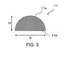
- FIG. 3 is a schematic cross-sectional view of the metal fiber composing the porous portion shown in FIG. 2 .
- FIG. 4 is a flow diagram showing the flow of the process of producing the reinforced porous metal foil according to the present invention.
- FIG. 5 is a schematic cross-sectional view showing an example of a rotating drum type foil production apparatus for producing the reinforced porous metal foil according to the present invention.
- FIG. 6 is a front view for schematically showing the rotating drum viewed from the water-absorbing material side in the direction of the arrow A in FIG. 5 .
- FIG. 7 is a perspective view schematically showing the reinforced porous metal foil roll according to the present invention, which is produced by using the rotating drum shown in FIG. 6 .
- FIG. 8 is an image obtained in Example A1 by observing the surface of the noncontact region, which is to be the porous portion, immediately after the beginning of the copper plating, under an optical microscope (at a magnification of 500 times) from straight above (at a tilt angle of 0°).
- FIG. 9 is an image obtained in Example A1 by observing the surface of the contact region, which is to be the reinforced portion, immediately after the beginning of the copper plating, under the optical microscope (at a magnification of 500 times) from straight above (at a tilt angle of 0°).
- FIG. 10 is an image obtained in Example A2 by observing the surface which did not contact the peelable layer of the porous portion of the reinforced porous metal foil according to the present invention, under the optical microscope (at a magnification of 500 times) from straight above (at a tilt angle of 0°).
- FIG. 11 is an image obtained in Example A2 by observing the surface which did not contact the peelable layer of the reinforcing region of the reinforced porous metal foil according to the present invention, under the optical microscope (at a magnification of 500 times) from straight above (at a tilt angle of 0°).
- FIG. 12 is an FE-SEM image obtained in Example B2 by observing the surface which did not contact the peelable layer of the porous metal foil (porous portion) from straight above (at a tilt angle of 0°).
- FIG. 13 is an FE-SEM image obtained in Example B2 by observing the surface which did not contact the peelable layer of the porous metal foil (porous portion) from obliquely above (at a tilt angle of 45°).
- FIG. 14 is an FE-SEM image obtained in Example B2 by observing the surface which contacted the peelable layer of the porous metal foil (porous portion) from straight above (at a tilt angle of 0°).
- FIG. 15 is an FE-SEM image obtained in Example B2 by observing the surface which contacted the peelable layer of the porous metal foil (porous portion) from obliquely above (at a tilt angle of 45°).
- FIG. 16 is a SIM image obtained in Example B2 by observing the cross-sectional surface formed by vertically cutting the metal fiber composing the porous metal foil (porous portion), at a tilt angle of 60°.
- FIG. 17 is a schematic view showing the fixation of a metal foil (porous portion) sample to fixtures in the tensile strength test conducted in Example B4.
- FIG. 18 is an FE-SEM image obtained in Example C2 by observing the surface which did not contact the peelable layer of the porous metal foil (porous portion) from straight above (at a tilt angle of 0°).
- FIG. 19 is an FE-SEM image obtained in Example C2 by observing the surface which contacted the peelable layer of the porous metal foil (porous portion) from straight above (at a tilt angle of 0°).
- FIG. 1 shows a schematic view of an example of the reinforced porous metal foil according to the present invention.
- the reinforced porous metal foil 10 according to the present invention comprises a porous portion 10 a and a reinforced portion 10 b .
- the porous portion 10 a comprises a two-dimensional network structure composed of a metal fiber 11 .
- the reinforced portion 10 b is a portion which is substantially non-porous or less porous than the porous portion 10 a , being composed of the same metal as the metal fiber 11 and being continuous and integral with the porous portion 10 a.
- the porous portion 10 a comprises a two-dimensional network structure composed of the metal fiber 11 .
- FIG. 2 shows a schematic top view of an example of the porous portion 10 a .
- the porous portion 10 a comprises a two-dimensional network structure composed of the metal fiber 11 .
- the porous portion 10 a has an aperture ratio of preferably 3 to 80%, more preferably 5 to 60%, further preferably 10 to 55%, and still further preferably 20 to 55%.
- W p /W n is the ratio of the weight W p of a porous metal foil to the theoretical weight W n of a non-porous metal foil having a composition and a size which are identical to those of the porous metal foil.
- This theoretical weight W n may be calculated by: measuring the size of the porous metal foil obtained; calculating the volume (i.e., the theoretical volume of the non-porous metal foil) from the measured size; and then multiplying the resultant volume by the density of the material of the porous metal foil prepared.
- the porous portion 10 a may have a tensile strength of preferably not less than 10N/10 mm, more preferably not less than 15N/10 mm, as measured according to the later-described measuring method, thus making it possible to effectively prevent the porous metal foil from breaking.
- a tensile strength lower than the above ranges are of no problem. In this case, it is possible to maximize the aperture ratio without concern for tensile strength.
- the porous metal foil 10 has a thickness of preferably 3 to 40 ⁇ m, more preferably 3 to 30 ⁇ m, further preferably 5 to 25 ⁇ m, still further preferably 10 to 20 ⁇ m, most preferably 10 to 15 ⁇ m. Within these ranges, a superior balance is achieved between high aperture ratio and high strength.
- the thickness of the porous metal foil corresponds to the maximum cross-sectional height of the metal fiber, since the porous metal foil of the present invention comprises the two-dimensional network structure composed of the metal fiber. The thickness is preferred to be measured by a commercially available film-thickness measuring device having a spindle which is larger than the pore sizes of the porous metal foil.
- the metal fiber 11 is a fiber made of metal, and the metal to be used may be suitably chosen depending on the intended use and is not particularly limited.
- Preferred metal comprises at least one selected from the group consisting of copper, aluminum, gold, silver, nickel, cobalt, and tin.
- the term “comprise” means that it embraces metal or alloy mainly containing metal element(s) as listed above, which may include other metal element(s) and unavoidable impurities as the balance, and preferably means that metal element(s) as listed above constitutes not less than 50% by weight of the metal or alloy, with a typical example being metal or alloy consisting of metal element(s) as listed above and unavoidable impurities.
- the above definition will be equally applied to similar expressions described hereinbelow with regard to metal.
- metal or alloy suitable for anode current collectors of electric storage devices includes metal or alloy comprising at least one selected from the group consisting of copper, copper alloys, nickel, cobalt, and tin, preferably copper.
- the two-dimensional network structure is preferred to have an irregular shape derived from a crack, which has been formed on the surface of a substrate.
- the fiber diameter of the metal fiber 11 is preferred to be 5 to 80 ⁇ m, more preferably 5 to 50 ⁇ m, further preferably 8 to 30 ⁇ m, most preferably 10 to 20 ⁇ m.
- the term “fiber diameter” is defined as the width (thickness) of the fiber 11 when the porous metal foil is viewed from straight above, and can be measured by using optical microscope, field emission scanning electron microscope (FE-SEM), scanning ion microscope (SIM) or the like. Within these ranges, a superior balance is achieved between high aperture ratio and high strength.
- the metal fiber 11 is a branched fiber, which is irregularly networked to constitute the porous portion 10 a .
- the fiber 11 is formed by numerous metal particles being connected to each other, resulting from nucleation along the later-mentioned crack in the peelable layer. Since it is desirable for the adjacent metal particles to tightly connect with each other through particle growth in order to constitute the metal fiber, the metal particles constituting the metal fiber may no longer have the complete shapes of the particles.
- the metal particles constituting the metal fiber 11 typically have hemispherical shapes having spherical parts 11 a and bottom parts 11 b .
- the bottom parts 11 b of all the metal particles are positioned on the same basal plane, while the spherical parts 11 a of all the metal particles are positioned to the same side with reference to the basal plane.
- the width D of the bottom part 11 b along the basal plane is the fiber diameter, while the maximum cross-sectional height H of the spherical part 11 a corresponds to the thickness of the porous metal foil.
- This basal plane and the bottom part 11 b positioned thereon have a shape corresponding to the flat plane shape of the peelable layer which is used during the production, although they are not limited to this shape when the foil is produced by other production methods.
- the average ratio of the maximum cross-sectional height H to the fiber diameter D of the fiber 11 is, but not limited to, typically 0.30 to 0.70, more typically 0.40 to 0.60, further typically 0.45 to 0.55, most typically about 0.50, and may be adjusted by modifying the plating conditions or the like as appropriate.
- the average area of the pores in the porous portion 10 a is, but not limited to, typically 3 to 5000 ⁇ m 2 , more typically 3 to 3000 ⁇ m 2 , further typically 3 to 2000 ⁇ m 2 .
- the ratio of the number of pores having areas of not more than one-half of the largest pore area to the number of the total pores is, but not limited to, typically not less than 60%, more typically not less than 70%, further typically not less than 80%.
- the reinforced portion 10 b is a portion which is substantially non-porous or less porous than the porous portion 10 a , being composed of the same metal as the metal fiber 11 and being continuous and integral with the porous portion 10 a .
- the reinforced portion 10 b is integrally formed with the porous portion 10 a using the same material, and has a shape that is continuous with the porous portion 10 a .
- the reinforced porous metal foil according to the present invention does not include a composite comprising the porous portion 10 a and the reinforced portion 10 b that were separately formed and combined later.
- the porous portion 10 a and the reinforced portion 10 b should be distinguished from each other in terms of the number of pores or the existence/absence of the pores, and should not be distinguished in terms of the constituent material or shape except for pore (for example, thickness). Therefore, the porous portion 10 a typically has a thickness equivalent or close to that of the reinforced portion 10 b . As needed, the thickness can be adjusted by controlling such conditions as current density, plating solution, plating solution flow rate, masking, etc.
- the existence of such a reinforced portion 10 b makes the porous metal foil less likely to break, and thus can facilitate conveyance of the porous metal foil in the production line. Furthermore, in a case where the porous metal foil is used as a current collector in an electricity storage device, it is possible to use the reinforced portion as a tab lead, thus improving the reliability in tab lead connection.
- the reinforced portion 10 b is provided as at least a part of the outer edge of the metal foil 10 . Since breakage such as splitting or tearing is more likely to occur in the outer edge of the porous metal foil than in the outer edge of the non-porous metal foil, composing such a portion as a reinforced portion makes it possible to effectively suppress the breakage of outer edge, thereby facilitating the production of a thin porous metal foil. For example, if the metal foil 10 has an elongated shape, it is preferable that the outer edges along the longitudinal direction of the metal foil 10 be composed of the reinforced portion 10 b.
- the reinforced portion 10 b may be provided away from and in parallel with outer edges along a longitudinal direction of the metal foil 10 .
- a metal foil can be slit in the longitudinal direction (and at regular intervals, for example) into a plurality of metal foil long strips.
- a porous metal foil is more likely to generate fragments such as swarf and machining dust during slitting, as compared to a non-porous metal foil.
- the portion to be slit composed of a reinforced portion it is possible to suppress the occurrence of fragments such as swarf and machining dust during slitting.
- the reinforced portions 10 b be provided as outer edges along the longitudinal direction of the metal foil 10 , as well as on lines that are away from and in parallel with the outer edges along the longitudinal direction 10 of the metal foil.
- the reinforced portions 10 b are preferably substantially non-porous from the viewpoint of reinforcement efficiency, ideally non-porous.
- the term “substantially” herein is intended to allow existence of holes, such as pinholes, which may be inevitably formed during production process. Nevertheless, as far as the reinforced portions can suppress the occurrence of breakage or fragments, it is sufficient if the reinforced portions have holes that are fewer than those of the porous portions. Thus, it is not always necessary that the reinforced portions are non-porous or substantially non-porous.
- porous metal foil according to the present invention is not limited to those produced by this production method but includes those produced by other production methods.
- FIG. 4 shows the flow of the process of producing the reinforced porous metal foil according to the present invention.
- an electrically conductive substrate 12 including a peelable layer 13 on the surface of which cracks are formed, is first provided as a support for producing the porous metal foil.
- the electrically conductive substrate 12 , on which the peelable layer 13 is to be formed may be a substrate having an electrical conductivity which enables plating thereon. Any of inorganic materials, organic materials, laminates, and materials having metallic surfaces can be used as the substrate, with metals being preferred.
- Preferred examples of such metals include metals, such as copper, nickel, cobalt, iron, chromium, tin, zinc, indium, silver, gold, aluminum, and titanium, and alloys containing at least one of these metal elements, more preferred examples being copper, copper alloys, nickel, nickel alloys, titanium, titanium alloys, and stainless steels.
- the configuration of the electrically conductive substrate is also not limited, allowing the use of substrates in various forms including foil, plate, and drum. In the case of drum, an electrically conductive metal plate may be used with the plate being wrapped around the drum. The thickness of the electrically conductive metal plate in this case is preferred to be 1 to 20 mm.
- the electrically conductive substrate supports the produced porous metal foil during its processing or until just before its use, thus improving the handleability of the porous metal foil.
- a metal foil as the electrically conductive substrate since there are advantages in that the metal foil used as the electrically conductive substrate can be reused as it is after the production of the porous metal foil, or can be recycled through melting and foil production.
- the thickness of the metal foil is preferred to be 10 ⁇ m to 1 mm as ensuring a strength which prevents wrinkles or twists and the like from generating during the metal foil production process and the subsequent processing-and-transporting process or the like.
- the shape of the crack in the peelable layer varies depending on the material and roughness of the electrically conductive substrate, and thus may change the properties of the porous metal foil, such as aperture ratio. On the other hand, it is a matter of course that the shape of the porous metal foil may change even depending on the type or conditions of the metal plating. In order to obtain a desired porous metal foil in consideration of these, selecting the electrically conductive substrate and setting the conditions for forming the peelable layer and/or those for plating may be done suitably depending on the necessity.
- the peelable layer 13 is then formed on the electrically conductive substrate 12 , with cracks 13 a being generated in the peelable layer 13 .
- pretreatment such as acid washing and degreasing
- the peelable layer 13 is a layer which facilitates the peeling of the porous metal foil 10 to be formed thereon, and is composed of a material which is capable of generating the cracks 13 a and has a tendency of being easily plated at the cracks 13 a as well as being hardly plated at regions 13 b where no cracks exist.
- this peelable layer 13 a material which allows a certain type of metal to preferentially deposit on the generated cracks 13 a by plating is used as the peelable layer 13 .
- this peelable layer may be formed in a multilayered manner, in which cracks may be formed only in the upper layer or otherwise cracks may be formed not only in the upper layer but also in the lower layer(s).
- An oxide film may be formed by anode oxidation method, etc. on the surface of the peelable layer, or a diamond-like carbon (DLC) or the like may be present on the surface of the peelable layer. It is preferred to control formation of the cracks 13 a so that cracks can spontaneously generate due to the stress in the peelable layer 13 .
- the cracks need not generate at the time of the formation of the peelable layer but may generate during the subsequent steps such as washing-and-drying process or machining process. Although cracks are usually undesirable, the production method of the present invention is characterized by rather taking advantage of the cracks in a positive way. In particular, since cracks usually have characteristics of being formed in a way such that branched lines are networked in a two-dimensional manner, forming metal fiber along the cracks can provide a porous metal foil having a high aperture ratio and a high strength.
- the peelable layer 13 comprises at least one selected from the group consisting of chromium, titanium, tantalum, niobium, nickel and tungsten or is composed of an organic material such as a resin.
- the peelable layer is more preferred to comprise at least one selected from the group consisting of chromium, titanium and nickel which have high hardness, in terms of continuous peelability, durability and corrosion resistance, is further preferred to comprise at least one selected from the group consisting of chromium and titanium, and is most preferred to be composed of chromium, a chromium alloy or a chromium oxide in that it forms passive state, which facilitates the peeling.
- the thickness of the peelable layer 13 is preferred to be in the range of 1 nm to 100 ⁇ m, more preferably 0.1 to 50 ⁇ m, further preferably 1 to 30 ⁇ m, most preferably 2 to 15 ⁇ m.
- These compositions and thicknesses enable generation of cracks, while providing the peelable layer with a higher resistance relative to the electrically conductive substrate to facilitate the formation and peeling of the porous metal foil 10 which is to be formed on the peelable layer. Therefore, the peelable layer is desired to be composed of a material having a resistance higher than that of the electrically conductive substrate.
- the peelable layer 13 can be formed by various film forming methods, which include, but not limited to, electrolytic plating, non-electrolytic plating, sputtering method, physical vapor deposition (PVD), chemical vapor deposition (CVD), sol-gel method, and ion-plating method. In terms of production efficiency or the like, it is preferable that the peelable layer 13 be also formed by electrolytic plating. As necessary, the peelable layer 13 may be further subjected to heat treatment and/or polishing, without departing from the spirit of the invention. Specifically, polishing is permitted to such an extent that the surface of the peelable layer 13 is merely cleansed, but it is a matter of course that polishing should not be conducted so excessively as to disfigure the cracks. Preferably, the peelable layer 13 thus obtained is washed with water or the like and then dried.
- preferred chromium plating solutions include Sargent bath and hard chromium plating baths, more preferably hard chromium plating baths.
- Preferred examples of commercially available hard chromium plating baths include Anchor 1127 produced by Meltex Inc., HEEF-25 produced by Atotech, and Mac-1 produced by Nihon MacDermid Co., Ltd. The bath compositions and electrolytic conditions are shown below, although it is permitted to depart from the following ranges as far as a desired porous metal foil is obtained.
- a stable chromium plating bath typically contains a small amount of trivalent chromium, of which the amount is about 2 to 6 g/L.
- a catalyst such as an organic sulfonic acid may also be added to the hard chromium plating bath.
- the concentration of chromic anhydride can be controlled in terms of Baume degree.
- impurities such as iron, copper and chloride ion, affect the plating condition, attention needs to be paid to control the maximum amount of dissolved impurities.
- An anode used for the chromium plating is preferred to be titanium coated with lead oxide or with a Pb—Sn alloy. Typical examples of such commercially available anodes include Ti—Pb electrode (Sn: 5%) produced by SPF Co., Ltd. and Exceload LD produced by Japan Carlit Co., Ltd.
- a pretreatment is performed by bringing a contact member into contact with a part of the peelable layer 13 , in which cracks are formed, and sliding the contact member thereon.
- This pretreatment makes it possible to obtain a reinforced portion, which is less porous or substantially non-porous than the porous portion, at the contacted portion in the subsequent plating process.
- by performing a pretreatment on a part on which a reinforced portion is to be formed it is possible to easily form a reinforced portion in a desired part of the porous metal foil.
- the contact member to be used in the pretreatment various members that can be in contact with the peelable layer can be used unless such members provide the peelable layer with an undesired defacement. Nevertheless, in order to apply the contact member to continuous production using a rotating drum etc., abrasion of the peelable layer caused by the contact with the contact member is desired to be small.
- the contact member is preferably a member that has no or very poor polishability such as a general water-absorbing material, or a member that has low polishability such as fine grit waterproof abrasive paper, more preferably, a member that has no or very poor polishability such as a general water-absorbing material. It is particularly preferable that the contact member contain water or an aqueous liquid.
- the water-absorbing materials may include various known materials that can contain water or aqueous liquid.
- the water-absorbing material include sponge, buff, sponge buff, cleaning buff, fabric, woven fabric, nonwoven fabric, waste cloth, absorbent cotton, and the combinations thereof, preferably cleaning buff.
- the liquid that may be contained in the water-absorbing material may be water or an aqueous liquid such as an aqueous solution in which some component is dissolved or dispersed in water within a range that does not depart from the spirit of the present invention. It is preferable that the aqueous solution contain no abrasive.
- the amount of the water or aqueous liquid contained in the water-absorbing material is not limited. As far as a desired effect can be obtained, the water-absorbing material may not contain water or an aqueous liquid.
- the peelable layer 13 thus pretreated is then plated with a metal capable of depositing preferentially on the cracks 13 a to grow numerous metal particles along the cracks 13 a in a region that has not been in contact with the contact member (hereinafter referred to as the “noncontact region”), thereby forming a porous portion 10 a , as well as to grow numerous metal particles in a region that has been in contact with the contact member (hereinafter referred to as the “contact region”) so as to be denser than those in the porous portion, thereby forming a reinforced portion 10 b .
- a metal capable of depositing preferentially on the cracks 13 a to grow numerous metal particles along the cracks 13 a in a region that has not been in contact with the contact member hereinafter referred to as the “noncontact region”
- the noncontact region of the peelable layer 13 has the cracks 13 a having a tendency of being easily plated thereon and the crack-free regions 13 b having a tendency of being hardly plated thereon.
- the reason why the cracks 13 a tend to be easily plated is that current flows more easily in parts where the cracks 13 a exist than in regions 13 b where no such cracks exist, resulting in preferential occurrence of nucleation and its growth on the cracks 13 a .
- the metal capable of depositing preferentially on the cracks 13 a preferably comprises at least one element selected from the group consisting of copper, aluminum, gold, silver, nickel, cobalt, and tin, more preferably at least one element selected from the group consisting of copper, gold, silver, nickel, cobalt, and tin, further preferably at least one element selected from the group consisting of copper, silver, and gold, most preferably, copper.
- the porous metal foil can be formed by plating methods with no particular limitation, which include electrolytic plating and non-electrolytic plating, between which electrolytic plating is preferable since it enables metal to deposit on the cracks 13 a efficiently.
- the plating conditions may be determined in accordance with known methods and are not particularly limited. For example, copper plating is preferred to be conducted in a copper sulfate plating bath.
- preferred plating bath compositions and electrodepositing conditions include, but not limited to, copper sulfate pentahydrate in a concentration of 120 to 350 g/L; sulfuric acid in a concentration of 50 to 200 g/L; a cathode current density of 10 to 80 A/dm 2 ; and a bath temperature of 40 to 60° C.
- An additive agent may be suitably added to the plating solution to enhance properties of the metal foil.
- additive agents include hide glues, gelatins, chlorine, sulfur-containing compounds such as thiourea, synthesized additive agents such as polyethylene glycols. With these preferred additive agents, it is possible to control dynamic properties and surface condition of the metal foil.
- concentration of the additive agent is not limited but is normally in the range of 1 to 300 ppm.
- the reinforced porous metal foil is peeled off from the electrically conductive substrate having the peelable layer to obtain an independent reinforced porous metal foil.
- the peeled foil may be transferred to another substrate such as a film provided with an adhesive layer thereon, or may be subjected to a surface treatment such as an anti-corrosive treatment.
- This peeling step is not essential, and the foil may be composed so that it can be handled as a porous metal foil product which remains provided with the substrate via the peelable layer and may not be peeled off until just before use.
- the porous metal foil can be more easily handled, while it becomes possible to significantly increase the aperture ratio or significantly reduce the film thickness because high strength is not so required due to the support by the substrate.
- the peelable layer Since the cracks still remain on the surface of the peelable layer, it is possible to reuse the peelable layer by subjecting it again to the contacting step with a contact member. However, increasing repetition of such reuse may lead to a decrease in the crack selectivity of the plating in the noncontact region, and thus may make it less likely to obtain a desired porous portion. In view of this, it is preferable to perform a step of drying the peelable layer to recover or maintain the crack selectivity of plating. That is, after the peeling step, the peelable layer, on which cracks have been made, remains on the surface of the electrically conductive substrate, and such an electrically conductive substrate provided with the peelable layer can be reused for a series of steps including the contact step, the plating step, and the peeling step.
- the decrease of the crack selectivity of the plating caused by the reuse can be prevented by the drying step.
- the conditions of the drying step are not particularly limited, but it is preferable that the drying step be performed at a temperature of 25 to 250° C.
- the peelable layer may be dried naturally.
- an electrically conductive substrate provided with a peelable layer may be configured in the form of a rotating drum, while the contact step, the plating step, the peeling step, and the drying step may be sequentially repeated by the rotation of the electrically conductive substrate.
- FIG. 5 shows a perspective sectional view of such a rotating drum type foil production apparatus. The foil production apparatus 20 shown in FIG.
- FIG. 5 includes a rotating drum 21 (for example, a stainless steel drum) formed of an electrically conductive substrate provided with a peelable layer (for example, a chromium plating layer) in the surface of which cracks are formed; an electroplating bath 22 in which a lower part of the rotating drum 21 is immersed in a plating solution; a water-absorbing material 23 positioned so that it can be in contact with a part of the peelable layer on the rotating drum; a water receptor 24 for receiving water dripping from the water-absorbing material; and a peeling roll 25 for peeling off the porous metal foil 10 from the rotating drum and conveying the porous metal foil 10 .
- FIG. 6 is a front view schematically showing the rotating drum 21 viewed from the water-absorbing material 23 in FIG.
- the foil production apparatus 20 may also include water supplying means for supplying water W to the water-absorbing material 23 , or may be configured to use a water-absorbing material that is soaked with water in advance.
- the water-absorbing material 23 becomes in contact with the surface of the rotating drum 21 (i.e., the peelable layer) and slides relative thereto to form an elongated region 21 b which has contacted by the water-absorbing material 23 , so that a foil portion prepared in contact with the region 21 b forms a reinforced portion 10 b .
- a foil portion prepared in contact with the region 21 a which has not been contacted by the water-absorbing material 23 forms a porous portion 10 a .
- the rotating drum is washed with water if desired, and is subjected to the drying step.
- heating means may be provided thereto to perform the drying step artificially.
- the rotating drum which underwent the drying step is rotated to be subjected to the contact step again, followed by the plating step, the peeling step, and the drying step. According to such an embodiment, it is possible to mass-produce a reinforced porous metal foil in a rolled form very effectively by using a rotating drum type foil production apparatus.
- porous metal foil Typical applications include anode current collectors of electric storage devices, such as lithium-ion secondary batteries and lithium-ion capacitors.
- the porous metal foil can be used in various applications, such as screening devices for fine-powder classification or solid-liquid separation, catalyst carriers, nets to be used in oxygen inlets of microorganism storage containers, dust-proof filters for clean rooms, antibacterial filters for liquids, filters for liquid reforming, electromagnetic-wave shields, magnetic materials, electrically conductive materials, and decoration sheets.
- porous metal foil when used as an inner layer of a printed board to work as an electrically conductive material or the like, it is possible, through the pores, to release a gas derived from a resin, a solvent or the like, so that generation of blisters can be prevented.
- using the porous metal foil for forming circuits as an electrically conductive material or the like can attain weight reduction of the circuits by reducing the metal usage.
- a stainless steel plate (SUS316) having a thickness of 1 mm was prepared as an electrically conductive substrate.
- a chromium plating for forming a peelable layer was performed on the stainless steel plate in the following manner.
- the surface of the electrode was cleaned by alkaline electrolytic degreasing using Endox 114 (an alkaline deruster produced by Meltex Inc.) under the conditions of a current density of 10 A/dm 2 , an electrolysis time of 10 minutes, and an anode being DSE (Dimensionally Stable Electrode). After washed with water, the degreased stainless steel plate was immersed in 50 ml/L sulfuric acid for 1 minute to be acid-activated.
- the acid-activated stainless steel plate was immersed in a chromium plating bath (HEEF 25 produced by Atotech) in which 250 g/L chromic anhydride, 3 g/L sulfuric acid, and 22 m/L HEEF 25C (produced by Atotech) were dissolved, and was subjected to a chromium plating under the conditions of a temperature of 55° C., a current density of 30 A/dm 2 , and an electrolysis time of 17 minutes. At this time, a Ti—Pb electrode (Pb—Sn 5%, produced by SPF Co., Ltd.) was used as the anode.
- the stainless steel plate on which the chromium plating was formed was washed with water and then dried. Numerous cracks, which are considered to have been formed by plating stress, were confirmed on the surface of the chromium plating obtained.
- a cleaning buff soaked with water (produced by Tsunoda Brush Co., Ltd. with the product name of “NA Cleaning Buff,” non-abrasive buff with polypropylene nonwoven material) was brought into contact with a part of the chromium plating in which the cracks were formed, and lightly slid thereon.
- the water contact angle on the surface of the chromium plating thus having been pretreated was measured.
- the water contact angle of the portion which has contacted the cleaning buff (hereinafter referred to as the “contact region”) was 25.8 degrees
- the water contact angle of the portion which has not contacted the cleaning buff (hereinafter referred to as the “noncontact region”) was 69.3 degrees.
- the water contact angle is defined as an angle ⁇ between the tangent of a water drop on a surface of a solid body and the surface of the solid body, and was evaluated by measuring the water contact angle after 10 seconds from the drop by using a contact angle measurement device (Kyowa Interface Science Co., Ltd., “Contact Angle Meter”).
- a copper sulfate plating was performed on the locally pretreated chromium plating in which the cracks were generated.
- the stainless steel plate, on which the chromium plating had been performed was immersed in a copper sulfate plating bath in which 250 g/L copper sulfate pentahydrate (having a copper concentration of about 64 g/L) and 80 g/L sulfuric acid were dissolved, and was plated under the conditions including a current density of 20 A/dm 2 , a plating time of 150 seconds, an anode being DSE (Dimensionally Stable Electrode), and a bath temperature of 40° C.
- DSE Dissionally Stable Electrode
- the noncontact region and the contact region immediately after the beginning of the copper plating were observed by an optical microscope (at the magnification of 500 times) to obtain images shown FIGS. 8 and 9 , respectively.
- FIG. 8 in the noncontact region, since current flows more easily through the crack part than the outermost surface of the chromium plating, copper particles originating from the cracks have grown.
- FIG. 9 in the contact region, copper particles deposited over the entire surface, instead of depositing selectively in the cracked portions.
- a metal foil comprising a porous portion which comprises a two-dimensional network structure composed of copper fibers formed on the chromium plating derived from the noncontact region; and a nonporous reinforced portion derived from the contact region.
- the porous metal foil was physically peeled off from the chromium plating to obtain a reinforced porous metal foil.
- the thickness of the copper foil obtained was 15 ⁇ m, and the weight aperture ratio was 34%.
- the reinforced porous metal foil obtained in Example A1 was observed by an optical microscope (at a magnification of 500 times).
- the side of the porous portion of the porous metal foil, which had not been in contact with the peelable layer (hereinafter referred to as the “growth side”) was observed from straight above (at a tilt angle of 0°) to obtain the image shown in FIG. 10 .
- the side of the reinforced portion of the porous metal foil, which had not been in contact with the peelable layer hereinafter referred to as the “growth side” was observed from straight above (at a tilt angle of 0°) to obtain the image shown in FIG. 11 .
- a two-dimensional network structure composed of metal fibers was observed in the porous portion, while a nonporous metal foil part was confirmed as the reinforced portion, in which no pore was observed.
- Copper foil having a thickness of 35 ⁇ m was prepared as an electrically conductive substrate.
- a chromium plating for forming a peelable layer was performed on the copper foil in the following manner.
- the copper foil was immersed for 2 minutes at 40° C. in an acidic cleaner for printed-wiring board (PAC-200 produced by Murata Co., Ltd.) of which the concentration was adjusted to 120 ml/L with added water.
- the copper foil thus cleansed was immersed in 50 ml/L sulfuric acid at room temperature for 1 minute to be acid-activated.
- the acid-activated copper foil was immersed in a chromium plating bath in which 180 g/L Econo-Chrome 300 (produced by Meltex Inc.) and 1 g/L pure concentrated sulfuric acid were dissolved, and was subjected to a chromium plating for 15 minutes under the conditions of a temperature of 45° C. and a current density of 20 A/dm 2 .
- the copper foil on which the chromium plating was formed was washed with water and then dried.
- the thickness of the resultant chromium plating was about 2 ⁇ m as measured by XRF (X-ray fluorescence analysis). Numerous cracks, which would have been formed by plating stress, were confirmed on the surface of the chromium plating.
- a copper sulfate plating was performed on the chromium plating where the cracks generated.
- the chromium-plated copper foil was immersed in a copper sulfate plating bath in which 250 g/L copper sulfate pentahydrate (having a copper concentration of about 64 g/L) and 80 g/L sulfuric acid were dissolved, and plated under the conditions including a current density of 20 A/dm 2 ; a plating time of 150 seconds; an anode being DSE (Dimensionally Stable Electrode); and a bath temperature of 40° C.
- DSE Dissionally Stable Electrode
- the porous metal foil obtained in Example B1 was observed by a field emission-scanning electron microscope (FE-SEM) from different angles.
- FE-SEM field emission-scanning electron microscope
- peelable side the other side which had been in contact with the peelable layer of the porous metal foil (hereinafter, peelable side) was also observed from straight above (at a tilt angle of 0°) and obliquely above (at a tilt angle of 45°) to obtain images shown in FIGS. 14 and 15 , respectively.
- peelable side the other side which had been in contact with the peelable layer of the porous metal foil
- a cross-sectional surface of the metal fiber of the porous metal foil was observed by a scanning ion microscope (SIM) to obtain an image shown in FIG. 16 , after having been processed by a focused ion beam processing apparatus (FIB).
- SIM scanning ion microscope
- FIB focused ion beam processing apparatus
- the ratio of the maximum cross-sectional height H to the fiber diameter D at the cross-sectional surface of the metal fiber was calculated to be about 0.50.
- the number of pores per unit area was about 300 mm ⁇ 2 .
- the largest pore area observed was about 4700 ⁇ m 2 , while the ratio of the number of pores having pore areas not more than one-half of the largest pore area (i.e., not more than about 2350 ⁇ m 2 ) to the number of the total pores was about 90%.
- the aperture ratio of the porous metal foil obtained in Example B1 was determined by weight method in the following manner.
- the thickness of the porous metal foil was measured to be 14.7 ⁇ m by a digital length measuring system (Digimicro MH-15M manufactured by Nikon Corporation).
- MS-5C manufactured by Nikon Corporation
- a spindle which is the standard equipment of Digimicro MH-15M was used.
- the unit weight per 100 mm ⁇ 100 mm square of the foil was measured to be 0.94 g.
- the theoretical weight of a non-porous copper foil having a thickness of 14.7 ⁇ m and an area of 100 mm ⁇ 100 mm square was calculated to be 1.31 g, using the copper density of 8.92 g/cm 3 . With these values, the aperture ratio of the porous metal foil was calculated to be 28% as shown below.
- the tensile strength of the porous metal foil obtained in Example B1 was measured in accordance with JIS C 6511-1992 as shown below.
- a test piece having a size of 10 mm ⁇ 100 mm was cut off from the porous metal foil.
- this test piece 30 was fixed with its both ends being held by an upper fixture 31 and a lower fixture 31 of a tensile strength tester (Autograph manufactured by Shimadzu Corporation) so that the distance between the two fixtures could be 50 mm.
- the tensile strength was then measured by stretching the test piece at a tension rate of 50 mm/minute. In this measurement, a load cell of 1 kN was used in the tensile strength tester.
- the porous metal foil according to the present invention is considered to have a strength endurable for practical use.
- a stainless steel plate made of SUS304 was prepared as an electrically conductive substrate.
- a chromium plating for forming a peelable layer with a thickness of 2 ⁇ m was performed on the stainless steel plate in the following manner.
- the stainless steel plate was immersed for 2 minutes at 40° C. in an acidic cleaner for printed-wiring board (PAC-200 produced by Murata Co., Ltd.) of which the concentration was adjusted to 120 ml/L with added water.
- the stainless steel plate thus cleansed was immersed in 50 ml/L sulfuric acid at room temperature for 1 minute to be acid-activated.
- the acid-activated stainless steel plate was immersed in a commercially available hard chromium plating bath (HEEF-25 produced by Atotech), and was subjected to a chromium plating under the conditions of a cathode current density of 20 A/dm 2 ; an electrolysis time of 400 seconds; a bath temperature of 45° C.; a coulomb amount of 8000 C/dm 2 ; an electrode area of 1.2 dm 2 ; and a distance between electrodes of 90 mm.
- the stainless steel plate on which the chromium plating was formed was washed with water and then dried.
- the thickness of the resultant chromium plating was about 2 ⁇ m as measured by XRF (X-ray fluorescence analysis). Numerous cracks, which would have been formed by plating stress, were confirmed on the surface of the chromium plating.
- a silver plating was performed on the chromium plating where the cracks generated.
- the chromium-plated stainless steel plate was immersed in a commercially available silver plating bath (Selenabright C produced by Japan Pure Chemical Co., Ltd.), in which 25 g/L potassium cyanide, silver potassium cyanide (50 g/L as silver), a phosphate and the like were dissolved, and plated under the conditions including a cathode current density of 1.0 A/dm 2 ; an electrolysis time of 469 seconds; and a bath temperature of 40° C.
- a commercially available silver plating bath Senabright C produced by Japan Pure Chemical Co., Ltd.
- 25 g/L potassium cyanide, silver potassium cyanide (50 g/L as silver), a phosphate and the like were dissolved, and plated under the conditions including a cathode current density of 1.0 A/dm 2 ; an electrolysis time of 469 seconds; and a bath temperature of 40° C
- porous metal foil As a result, a two-dimensional network structure composed of silver fibers was formed, as a porous metal foil, on the chromium plating. Finally, the porous metal foil was physically peeled off from the chromium plating to obtain an isolated porous metal foil (porous portion).
- the porous metal foil obtained in Example C1 was observed by a field emission-scanning electron microscope (FE-SEM) from different angles.
- FE-SEM field emission-scanning electron microscope
- the side which had not been in contact with the peelable layer of the porous metal foil (hereinafter, growth side) was observed from straight above (at a tilt angle of 0°) to obtain an image shown in FIG. 18 .
- peelable side was also observed from straight above (at a tilt angle of 0°) to obtain an image shown in FIG. 19 .
- the largest pore area observed was about 462 ⁇ m 2 , while the ratio of the number of pores having pore areas not more than one-half of the largest pore area (i.e., not more than about 231 ⁇ m 2 ) to the number of the total pores was about 97%.
- the aperture ratio of the porous metal foil obtained in Example C1 was determined by weight method in the following manner.
- the thickness of the porous metal foil was measured to be 6.4 ⁇ m by a digital length measuring system (Digimicro MH-15M manufactured by Nikon Corporation).
- MS-5C manufactured by Nikon Corporation
- a spindle which is the standard equipment of Digimicro MH-15M was used.
- the unit weight per 100 mm ⁇ 100 mm square of the foil was measured to be 0.450 g.
- the theoretical weight of a non-porous silver foil having a thickness of 6.4 ⁇ m and an area of 100 mm ⁇ 100 mm square was calculated to be 0.672 g, using the silver density of 10.49 g/cm 3 . With these values, the aperture ratio of the porous metal foil was calculated to be 33% as shown below.
Landscapes
- Chemical & Material Sciences (AREA)
- Engineering & Computer Science (AREA)
- Chemical Kinetics & Catalysis (AREA)
- Electrochemistry (AREA)
- Materials Engineering (AREA)
- Power Engineering (AREA)
- Organic Chemistry (AREA)
- Metallurgy (AREA)
- Microelectronics & Electronic Packaging (AREA)
- General Chemical & Material Sciences (AREA)
- Manufacturing & Machinery (AREA)
- Cell Electrode Carriers And Collectors (AREA)
- Electroplating Methods And Accessories (AREA)
- Electric Double-Layer Capacitors Or The Like (AREA)
Applications Claiming Priority (3)
| Application Number | Priority Date | Filing Date | Title |
|---|---|---|---|
| JP2011005111A JP5636291B2 (ja) | 2011-01-13 | 2011-01-13 | 補強された多孔質金属箔およびその製造方法 |
| JP2011-005111 | 2011-03-04 | ||
| PCT/JP2012/050189 WO2012096233A1 (ja) | 2011-01-13 | 2012-01-06 | 補強された多孔質金属箔およびその製造方法 |
Publications (2)
| Publication Number | Publication Date |
|---|---|
| US20130216849A1 US20130216849A1 (en) | 2013-08-22 |
| US9512527B2 true US9512527B2 (en) | 2016-12-06 |
Family
ID=46507133
Family Applications (1)
| Application Number | Title | Priority Date | Filing Date |
|---|---|---|---|
| US13/882,530 Expired - Fee Related US9512527B2 (en) | 2011-01-13 | 2012-01-06 | Reinforced porous metal foil and process for production thereof |
Country Status (6)
| Country | Link |
|---|---|
| US (1) | US9512527B2 (enExample) |
| JP (1) | JP5636291B2 (enExample) |
| KR (1) | KR101483574B1 (enExample) |
| CN (1) | CN103282552B (enExample) |
| TW (1) | TWI439574B (enExample) |
| WO (1) | WO2012096233A1 (enExample) |
Cited By (1)
| Publication number | Priority date | Publication date | Assignee | Title |
|---|---|---|---|---|
| US10249434B2 (en) | 2015-08-12 | 2019-04-02 | Murata Manufacturing Co., Ltd. | Capacitor |
Families Citing this family (14)
| Publication number | Priority date | Publication date | Assignee | Title |
|---|---|---|---|---|
| KR101582376B1 (ko) * | 2013-06-07 | 2016-01-04 | 주식회사 제낙스 | 전극, 이의 제조 방법 및 이를 이용한 전지 |
| US9583277B2 (en) * | 2013-09-30 | 2017-02-28 | The Paper Battery Company, Inc. | Ultra-capacitor structures and electronic systems with ultra-capacitor structures |
| JP6398998B2 (ja) * | 2014-02-07 | 2018-10-03 | 株式会社村田製作所 | コンデンサ |
| FR3029386A1 (fr) * | 2014-11-28 | 2016-06-03 | Commissariat Energie Atomique | Blindage magnetique ameliore |
| JP2017001312A (ja) * | 2015-06-11 | 2017-01-05 | 吉田 英夫 | ワークの皮膜形成構造およびワークの皮膜形成方法 |
| TWI687949B (zh) * | 2016-03-31 | 2020-03-11 | 日商日本貴彌功股份有限公司 | 電極箔、電極箔的製造方法及捲繞型電容器的製造方法 |
| JP6978262B2 (ja) * | 2017-09-22 | 2021-12-08 | セーレン株式会社 | 通気性防水金属箔 |
| JP2019173164A (ja) * | 2018-03-28 | 2019-10-10 | 日立金属株式会社 | アルミニウム箔の製造方法 |
| CN108436100B (zh) * | 2018-04-09 | 2021-06-04 | 哈尔滨工业大学(深圳) | 一种超薄多孔纳米镍箔的制备方法 |
| KR102378651B1 (ko) * | 2019-03-29 | 2022-03-25 | 한양대학교 에리카산학협력단 | 이차전지용 물질막 및 그 제조 방법 |
| JP7546246B2 (ja) | 2020-07-07 | 2024-09-06 | 星和電機株式会社 | 多孔質銅およびその製造方法 |
| CN117242603A (zh) * | 2022-02-28 | 2023-12-15 | 宁德时代新能源科技股份有限公司 | 负极极片、电极组件、电池单体、电池、用电设备及负极极片的制造方法和设备 |
| WO2024048565A1 (ja) * | 2022-08-30 | 2024-03-07 | 三井金属鉱業株式会社 | 金属不織布及びそれを用いてなる電極 |
| WO2025005272A1 (ja) * | 2023-06-29 | 2025-01-02 | 三井金属鉱業株式会社 | 被膜構造体の製造方法、及び被膜構造体 |
Citations (12)
| Publication number | Priority date | Publication date | Assignee | Title |
|---|---|---|---|---|
| US5030233A (en) | 1984-10-17 | 1991-07-09 | Paul Ducheyne | Porous flexible metal fiber material for surgical implantation |
| US5496650A (en) * | 1993-09-14 | 1996-03-05 | Katayama Special Industries, Ltd. | Metallic porous sheet having pores surrounded by a three-dimensional net-shaped framework of metallic layers |
| GB2320724A (en) | 1996-12-27 | 1998-07-01 | Fukuda Metal Foil Powder | Method for producing metal foil by electroforming |
| JPH1167222A (ja) | 1997-08-22 | 1999-03-09 | Kazuo Tagawa | 電池用集電体およびこれを用いた電池 |
| EP1038994A1 (en) | 1998-09-14 | 2000-09-27 | Mitsui Mining & Smelting Co., Ltd. | Porous copper foil, use thereof and method for preparation thereof |
| JP2000328284A (ja) | 1999-05-18 | 2000-11-28 | Sumitomo Metal Steel Products Inc | 多孔金属箔製造用の電着ドラム |
| WO2002000966A1 (en) * | 2000-06-27 | 2002-01-03 | Stork Prints B.V. | Electroforming die, method of manufacturing the same, application thereof and electroformed products |
| US6465133B1 (en) * | 1999-05-26 | 2002-10-15 | Sumitomo Electric Industries, Ltd. | Metallic porous body and method of manufacturing the same and battery current collector having the same |
| US20040115536A1 (en) * | 2001-01-29 | 2004-06-17 | Blankenborg Stephanus Gerardus Johannes | Method for producing electrical conductors, a solar collector, an electrochemical cell and use of conductors produced in this way |
| JP2005251429A (ja) | 2004-03-01 | 2005-09-15 | Mitsui Mining & Smelting Co Ltd | Al合金キャリア付孔開き金属箔及びその製造方法並びにAl合金キャリア付孔開き金属箔から分離された該孔開き金属箔を含む二次電池用電極及び二次電池 |
| WO2008081904A1 (ja) | 2006-12-27 | 2008-07-10 | Hitachi Chemical Co., Ltd. | 凹版及びこれを用いた導体層パターン付き基材 |
| WO2010034949A1 (fr) | 2008-09-25 | 2010-04-01 | Saint-Gobain Glass France | Procede de fabrication d'une grille submillimetrique electroconductrice, grille submillimetrique electroconductrice |
Family Cites Families (2)
| Publication number | Priority date | Publication date | Assignee | Title |
|---|---|---|---|---|
| JP2001202968A (ja) * | 2000-01-17 | 2001-07-27 | Dainippon Printing Co Ltd | 電池用集電体 |
| CN2676421Y (zh) * | 2003-11-05 | 2005-02-02 | 邝达辉 | 一种用于制造电极的折边金属扩张网带 |
-
2011
- 2011-01-13 JP JP2011005111A patent/JP5636291B2/ja active Active
-
2012
- 2012-01-06 KR KR1020137014259A patent/KR101483574B1/ko active Active
- 2012-01-06 US US13/882,530 patent/US9512527B2/en not_active Expired - Fee Related
- 2012-01-06 WO PCT/JP2012/050189 patent/WO2012096233A1/ja not_active Ceased
- 2012-01-06 CN CN201280005334.7A patent/CN103282552B/zh not_active Expired - Fee Related
- 2012-01-12 TW TW101101247A patent/TWI439574B/zh not_active IP Right Cessation
Patent Citations (17)
| Publication number | Priority date | Publication date | Assignee | Title |
|---|---|---|---|---|
| US5030233A (en) | 1984-10-17 | 1991-07-09 | Paul Ducheyne | Porous flexible metal fiber material for surgical implantation |
| US5496650A (en) * | 1993-09-14 | 1996-03-05 | Katayama Special Industries, Ltd. | Metallic porous sheet having pores surrounded by a three-dimensional net-shaped framework of metallic layers |
| GB2320724A (en) | 1996-12-27 | 1998-07-01 | Fukuda Metal Foil Powder | Method for producing metal foil by electroforming |
| JPH10195689A (ja) | 1996-12-27 | 1998-07-28 | Fukuda Metal Foil & Powder Co Ltd | 微細孔明き金属箔の製造方法 |
| JPH1167222A (ja) | 1997-08-22 | 1999-03-09 | Kazuo Tagawa | 電池用集電体およびこれを用いた電池 |
| JP3262558B2 (ja) | 1998-09-14 | 2002-03-04 | 三井金属鉱業株式会社 | 多孔質銅箔およびその用途ならびにその製造方法 |
| EP1038994A1 (en) | 1998-09-14 | 2000-09-27 | Mitsui Mining & Smelting Co., Ltd. | Porous copper foil, use thereof and method for preparation thereof |
| JP2000328284A (ja) | 1999-05-18 | 2000-11-28 | Sumitomo Metal Steel Products Inc | 多孔金属箔製造用の電着ドラム |
| US6465133B1 (en) * | 1999-05-26 | 2002-10-15 | Sumitomo Electric Industries, Ltd. | Metallic porous body and method of manufacturing the same and battery current collector having the same |
| WO2002000966A1 (en) * | 2000-06-27 | 2002-01-03 | Stork Prints B.V. | Electroforming die, method of manufacturing the same, application thereof and electroformed products |
| US20040115536A1 (en) * | 2001-01-29 | 2004-06-17 | Blankenborg Stephanus Gerardus Johannes | Method for producing electrical conductors, a solar collector, an electrochemical cell and use of conductors produced in this way |
| JP2005251429A (ja) | 2004-03-01 | 2005-09-15 | Mitsui Mining & Smelting Co Ltd | Al合金キャリア付孔開き金属箔及びその製造方法並びにAl合金キャリア付孔開き金属箔から分離された該孔開き金属箔を含む二次電池用電極及び二次電池 |
| WO2008081904A1 (ja) | 2006-12-27 | 2008-07-10 | Hitachi Chemical Co., Ltd. | 凹版及びこれを用いた導体層パターン付き基材 |
| CN101557927A (zh) | 2006-12-27 | 2009-10-14 | 日立化成工业株式会社 | 凹版和使用该凹版的带有导体层图形的基材 |
| US20100021695A1 (en) * | 2006-12-27 | 2010-01-28 | Susumu Naoyuki | Engraved plate and substrate with conductor layer pattern using the same |
| WO2010034949A1 (fr) | 2008-09-25 | 2010-04-01 | Saint-Gobain Glass France | Procede de fabrication d'une grille submillimetrique electroconductrice, grille submillimetrique electroconductrice |
| US20110247859A1 (en) | 2008-09-25 | 2011-10-13 | Georges Zagdoun | Method for manufacturing a submillimetric electrically conductive grid, and submillimetric electrically conductive grid |
Non-Patent Citations (5)
| Title |
|---|
| Chinese Office Action (With English Translation), Chinese Application No. 201280005334.7, dated Feb. 25, 2015 (18 pages). |
| International Search Report and Written Opinion dated Apr. 17, 2012 (with English translation). |
| Japanese Office Action (Application No. 2011-005111) dated Aug. 13, 2014. |
| Korean Office Action (Application No. 10-2013-7014259) dated Jun. 24, 2014 (with English translation). |
| Taiwanese Office Action (Application No. 101101247) dated Dec. 4, 2013 (with English translation). |
Cited By (1)
| Publication number | Priority date | Publication date | Assignee | Title |
|---|---|---|---|---|
| US10249434B2 (en) | 2015-08-12 | 2019-04-02 | Murata Manufacturing Co., Ltd. | Capacitor |
Also Published As
| Publication number | Publication date |
|---|---|
| JP2012144790A (ja) | 2012-08-02 |
| CN103282552A (zh) | 2013-09-04 |
| TWI439574B (zh) | 2014-06-01 |
| TW201307617A (zh) | 2013-02-16 |
| JP5636291B2 (ja) | 2014-12-03 |
| WO2012096233A1 (ja) | 2012-07-19 |
| KR101483574B1 (ko) | 2015-01-16 |
| CN103282552B (zh) | 2016-04-27 |
| US20130216849A1 (en) | 2013-08-22 |
| KR20130107327A (ko) | 2013-10-01 |
Similar Documents
| Publication | Publication Date | Title |
|---|---|---|
| US9512527B2 (en) | Reinforced porous metal foil and process for production thereof | |
| US8497026B2 (en) | Porous metal foil and production method therefor | |
| US8980438B2 (en) | Porous metal foil and production method therefor | |
| US9595719B2 (en) | Composite metal foil and production method therefor | |
| KR101832251B1 (ko) | 고내식성을 갖는 금속 다공체 및 그의 제조 방법 | |
| JP5691107B2 (ja) | 高耐食性を有する金属多孔体及びその製造方法 | |
| JP2013133504A (ja) | 金属多孔体の製造方法及び金属多孔体 | |
| JP2012144790A5 (enExample) | ||
| JP4298578B2 (ja) | キャリア箔付き多孔質金属箔及びその製造方法 |
Legal Events
| Date | Code | Title | Description |
|---|---|---|---|
| AS | Assignment |
Owner name: MITSUI MINING & SMELTING CO., LTD., JAPAN Free format text: ASSIGNMENT OF ASSIGNORS INTEREST;ASSIGNORS:MATSUNAGA, TETSUHIRO;NISHIKAWA, JOE;WATANABE, HAJIME;SIGNING DATES FROM 20130416 TO 20130422;REEL/FRAME:030314/0602 |
|
| STCF | Information on status: patent grant |
Free format text: PATENTED CASE |
|
| MAFP | Maintenance fee payment |
Free format text: PAYMENT OF MAINTENANCE FEE, 4TH YEAR, LARGE ENTITY (ORIGINAL EVENT CODE: M1551); ENTITY STATUS OF PATENT OWNER: LARGE ENTITY Year of fee payment: 4 |
|
| FEPP | Fee payment procedure |
Free format text: MAINTENANCE FEE REMINDER MAILED (ORIGINAL EVENT CODE: REM.); ENTITY STATUS OF PATENT OWNER: LARGE ENTITY |
|
| LAPS | Lapse for failure to pay maintenance fees |
Free format text: PATENT EXPIRED FOR FAILURE TO PAY MAINTENANCE FEES (ORIGINAL EVENT CODE: EXP.); ENTITY STATUS OF PATENT OWNER: LARGE ENTITY |
|
| STCH | Information on status: patent discontinuation |
Free format text: PATENT EXPIRED DUE TO NONPAYMENT OF MAINTENANCE FEES UNDER 37 CFR 1.362 |
|
| FP | Lapsed due to failure to pay maintenance fee |
Effective date: 20241206 |