US9502327B2 - Semiconductor device and method for manufacturing the same - Google Patents
Semiconductor device and method for manufacturing the same Download PDFInfo
- Publication number
- US9502327B2 US9502327B2 US14/913,719 US201514913719A US9502327B2 US 9502327 B2 US9502327 B2 US 9502327B2 US 201514913719 A US201514913719 A US 201514913719A US 9502327 B2 US9502327 B2 US 9502327B2
- Authority
- US
- United States
- Prior art keywords
- solder
- metal member
- semiconductor element
- semiconductor device
- terminal
- Prior art date
- Legal status (The legal status is an assumption and is not a legal conclusion. Google has not performed a legal analysis and makes no representation as to the accuracy of the status listed.)
- Active
Links
Images


Classifications
-
- H—ELECTRICITY
- H01—ELECTRIC ELEMENTS
- H01L—SEMICONDUCTOR DEVICES NOT COVERED BY CLASS H10
- H01L23/00—Details of semiconductor or other solid state devices
- H01L23/34—Arrangements for cooling, heating, ventilating or temperature compensation ; Temperature sensing arrangements
- H01L23/36—Selection of materials, or shaping, to facilitate cooling or heating, e.g. heatsinks
- H01L23/367—Cooling facilitated by shape of device
- H01L23/3675—Cooling facilitated by shape of device characterised by the shape of the housing
-
- B—PERFORMING OPERATIONS; TRANSPORTING
- B23—MACHINE TOOLS; METAL-WORKING NOT OTHERWISE PROVIDED FOR
- B23K—SOLDERING OR UNSOLDERING; WELDING; CLADDING OR PLATING BY SOLDERING OR WELDING; CUTTING BY APPLYING HEAT LOCALLY, e.g. FLAME CUTTING; WORKING BY LASER BEAM
- B23K1/00—Soldering, e.g. brazing, or unsoldering
- B23K1/0008—Soldering, e.g. brazing, or unsoldering specially adapted for particular articles or work
- B23K1/0016—Brazing of electronic components
-
- B—PERFORMING OPERATIONS; TRANSPORTING
- B23—MACHINE TOOLS; METAL-WORKING NOT OTHERWISE PROVIDED FOR
- B23K—SOLDERING OR UNSOLDERING; WELDING; CLADDING OR PLATING BY SOLDERING OR WELDING; CUTTING BY APPLYING HEAT LOCALLY, e.g. FLAME CUTTING; WORKING BY LASER BEAM
- B23K1/00—Soldering, e.g. brazing, or unsoldering
- B23K1/008—Soldering within a furnace
-
- B—PERFORMING OPERATIONS; TRANSPORTING
- B23—MACHINE TOOLS; METAL-WORKING NOT OTHERWISE PROVIDED FOR
- B23K—SOLDERING OR UNSOLDERING; WELDING; CLADDING OR PLATING BY SOLDERING OR WELDING; CUTTING BY APPLYING HEAT LOCALLY, e.g. FLAME CUTTING; WORKING BY LASER BEAM
- B23K3/00—Tools, devices, or special appurtenances for soldering, e.g. brazing, or unsoldering, not specially adapted for particular methods
- B23K3/08—Auxiliary devices therefor
- B23K3/087—Soldering or brazing jigs, fixtures or clamping means
-
- H—ELECTRICITY
- H01—ELECTRIC ELEMENTS
- H01L—SEMICONDUCTOR DEVICES NOT COVERED BY CLASS H10
- H01L23/00—Details of semiconductor or other solid state devices
- H01L23/34—Arrangements for cooling, heating, ventilating or temperature compensation ; Temperature sensing arrangements
- H01L23/42—Fillings or auxiliary members in containers or encapsulations selected or arranged to facilitate heating or cooling
- H01L23/433—Auxiliary members in containers characterised by their shape, e.g. pistons
- H01L23/4334—Auxiliary members in encapsulations
-
- H—ELECTRICITY
- H01—ELECTRIC ELEMENTS
- H01L—SEMICONDUCTOR DEVICES NOT COVERED BY CLASS H10
- H01L23/00—Details of semiconductor or other solid state devices
- H01L23/48—Arrangements for conducting electric current to or from the solid state body in operation, e.g. leads, terminal arrangements ; Selection of materials therefor
- H01L23/488—Arrangements for conducting electric current to or from the solid state body in operation, e.g. leads, terminal arrangements ; Selection of materials therefor consisting of soldered or bonded constructions
- H01L23/495—Lead-frames or other flat leads
- H01L23/49503—Lead-frames or other flat leads characterised by the die pad
- H01L23/49513—Lead-frames or other flat leads characterised by the die pad having bonding material between chip and die pad
-
- H—ELECTRICITY
- H01—ELECTRIC ELEMENTS
- H01L—SEMICONDUCTOR DEVICES NOT COVERED BY CLASS H10
- H01L23/00—Details of semiconductor or other solid state devices
- H01L23/48—Arrangements for conducting electric current to or from the solid state body in operation, e.g. leads, terminal arrangements ; Selection of materials therefor
- H01L23/488—Arrangements for conducting electric current to or from the solid state body in operation, e.g. leads, terminal arrangements ; Selection of materials therefor consisting of soldered or bonded constructions
- H01L23/495—Lead-frames or other flat leads
- H01L23/49541—Geometry of the lead-frame
- H01L23/49562—Geometry of the lead-frame for devices being provided for in H01L29/00
-
- H—ELECTRICITY
- H01—ELECTRIC ELEMENTS
- H01L—SEMICONDUCTOR DEVICES NOT COVERED BY CLASS H10
- H01L23/00—Details of semiconductor or other solid state devices
- H01L23/48—Arrangements for conducting electric current to or from the solid state body in operation, e.g. leads, terminal arrangements ; Selection of materials therefor
- H01L23/488—Arrangements for conducting electric current to or from the solid state body in operation, e.g. leads, terminal arrangements ; Selection of materials therefor consisting of soldered or bonded constructions
- H01L23/495—Lead-frames or other flat leads
- H01L23/49575—Assemblies of semiconductor devices on lead frames
-
- H—ELECTRICITY
- H01—ELECTRIC ELEMENTS
- H01L—SEMICONDUCTOR DEVICES NOT COVERED BY CLASS H10
- H01L24/00—Arrangements for connecting or disconnecting semiconductor or solid-state bodies; Methods or apparatus related thereto
- H01L24/01—Means for bonding being attached to, or being formed on, the surface to be connected, e.g. chip-to-package, die-attach, "first-level" interconnects; Manufacturing methods related thereto
- H01L24/26—Layer connectors, e.g. plate connectors, solder or adhesive layers; Manufacturing methods related thereto
- H01L24/31—Structure, shape, material or disposition of the layer connectors after the connecting process
- H01L24/32—Structure, shape, material or disposition of the layer connectors after the connecting process of an individual layer connector
-
- H—ELECTRICITY
- H01—ELECTRIC ELEMENTS
- H01L—SEMICONDUCTOR DEVICES NOT COVERED BY CLASS H10
- H01L24/00—Arrangements for connecting or disconnecting semiconductor or solid-state bodies; Methods or apparatus related thereto
- H01L24/01—Means for bonding being attached to, or being formed on, the surface to be connected, e.g. chip-to-package, die-attach, "first-level" interconnects; Manufacturing methods related thereto
- H01L24/26—Layer connectors, e.g. plate connectors, solder or adhesive layers; Manufacturing methods related thereto
- H01L24/31—Structure, shape, material or disposition of the layer connectors after the connecting process
- H01L24/33—Structure, shape, material or disposition of the layer connectors after the connecting process of a plurality of layer connectors
-
- H—ELECTRICITY
- H01—ELECTRIC ELEMENTS
- H01L—SEMICONDUCTOR DEVICES NOT COVERED BY CLASS H10
- H01L24/00—Arrangements for connecting or disconnecting semiconductor or solid-state bodies; Methods or apparatus related thereto
- H01L24/80—Methods for connecting semiconductor or other solid state bodies using means for bonding being attached to, or being formed on, the surface to be connected
- H01L24/83—Methods for connecting semiconductor or other solid state bodies using means for bonding being attached to, or being formed on, the surface to be connected using a layer connector
-
- B—PERFORMING OPERATIONS; TRANSPORTING
- B23—MACHINE TOOLS; METAL-WORKING NOT OTHERWISE PROVIDED FOR
- B23K—SOLDERING OR UNSOLDERING; WELDING; CLADDING OR PLATING BY SOLDERING OR WELDING; CUTTING BY APPLYING HEAT LOCALLY, e.g. FLAME CUTTING; WORKING BY LASER BEAM
- B23K2101/00—Articles made by soldering, welding or cutting
- B23K2101/36—Electric or electronic devices
- B23K2101/40—Semiconductor devices
-
- B23K2201/40—
-
- H—ELECTRICITY
- H01—ELECTRIC ELEMENTS
- H01L—SEMICONDUCTOR DEVICES NOT COVERED BY CLASS H10
- H01L2224/00—Indexing scheme for arrangements for connecting or disconnecting semiconductor or solid-state bodies and methods related thereto as covered by H01L24/00
- H01L2224/01—Means for bonding being attached to, or being formed on, the surface to be connected, e.g. chip-to-package, die-attach, "first-level" interconnects; Manufacturing methods related thereto
- H01L2224/02—Bonding areas; Manufacturing methods related thereto
- H01L2224/04—Structure, shape, material or disposition of the bonding areas prior to the connecting process
- H01L2224/05—Structure, shape, material or disposition of the bonding areas prior to the connecting process of an individual bonding area
- H01L2224/0554—External layer
- H01L2224/0555—Shape
- H01L2224/05552—Shape in top view
- H01L2224/05554—Shape in top view being square
-
- H—ELECTRICITY
- H01—ELECTRIC ELEMENTS
- H01L—SEMICONDUCTOR DEVICES NOT COVERED BY CLASS H10
- H01L2224/00—Indexing scheme for arrangements for connecting or disconnecting semiconductor or solid-state bodies and methods related thereto as covered by H01L24/00
- H01L2224/01—Means for bonding being attached to, or being formed on, the surface to be connected, e.g. chip-to-package, die-attach, "first-level" interconnects; Manufacturing methods related thereto
- H01L2224/02—Bonding areas; Manufacturing methods related thereto
- H01L2224/04—Structure, shape, material or disposition of the bonding areas prior to the connecting process
- H01L2224/06—Structure, shape, material or disposition of the bonding areas prior to the connecting process of a plurality of bonding areas
- H01L2224/0601—Structure
- H01L2224/0603—Bonding areas having different sizes, e.g. different heights or widths
-
- H—ELECTRICITY
- H01—ELECTRIC ELEMENTS
- H01L—SEMICONDUCTOR DEVICES NOT COVERED BY CLASS H10
- H01L2224/00—Indexing scheme for arrangements for connecting or disconnecting semiconductor or solid-state bodies and methods related thereto as covered by H01L24/00
- H01L2224/01—Means for bonding being attached to, or being formed on, the surface to be connected, e.g. chip-to-package, die-attach, "first-level" interconnects; Manufacturing methods related thereto
- H01L2224/26—Layer connectors, e.g. plate connectors, solder or adhesive layers; Manufacturing methods related thereto
- H01L2224/2612—Auxiliary members for layer connectors, e.g. spacers
-
- H—ELECTRICITY
- H01—ELECTRIC ELEMENTS
- H01L—SEMICONDUCTOR DEVICES NOT COVERED BY CLASS H10
- H01L2224/00—Indexing scheme for arrangements for connecting or disconnecting semiconductor or solid-state bodies and methods related thereto as covered by H01L24/00
- H01L2224/01—Means for bonding being attached to, or being formed on, the surface to be connected, e.g. chip-to-package, die-attach, "first-level" interconnects; Manufacturing methods related thereto
- H01L2224/26—Layer connectors, e.g. plate connectors, solder or adhesive layers; Manufacturing methods related thereto
- H01L2224/28—Structure, shape, material or disposition of the layer connectors prior to the connecting process
- H01L2224/29—Structure, shape, material or disposition of the layer connectors prior to the connecting process of an individual layer connector
- H01L2224/29001—Core members of the layer connector
- H01L2224/29099—Material
- H01L2224/291—Material with a principal constituent of the material being a metal or a metalloid, e.g. boron [B], silicon [Si], germanium [Ge], arsenic [As], antimony [Sb], tellurium [Te] and polonium [Po], and alloys thereof
- H01L2224/29101—Material with a principal constituent of the material being a metal or a metalloid, e.g. boron [B], silicon [Si], germanium [Ge], arsenic [As], antimony [Sb], tellurium [Te] and polonium [Po], and alloys thereof the principal constituent melting at a temperature of less than 400°C
-
- H—ELECTRICITY
- H01—ELECTRIC ELEMENTS
- H01L—SEMICONDUCTOR DEVICES NOT COVERED BY CLASS H10
- H01L2224/00—Indexing scheme for arrangements for connecting or disconnecting semiconductor or solid-state bodies and methods related thereto as covered by H01L24/00
- H01L2224/01—Means for bonding being attached to, or being formed on, the surface to be connected, e.g. chip-to-package, die-attach, "first-level" interconnects; Manufacturing methods related thereto
- H01L2224/26—Layer connectors, e.g. plate connectors, solder or adhesive layers; Manufacturing methods related thereto
- H01L2224/31—Structure, shape, material or disposition of the layer connectors after the connecting process
- H01L2224/32—Structure, shape, material or disposition of the layer connectors after the connecting process of an individual layer connector
- H01L2224/321—Disposition
- H01L2224/32151—Disposition the layer connector connecting between a semiconductor or solid-state body and an item not being a semiconductor or solid-state body, e.g. chip-to-substrate, chip-to-passive
- H01L2224/32221—Disposition the layer connector connecting between a semiconductor or solid-state body and an item not being a semiconductor or solid-state body, e.g. chip-to-substrate, chip-to-passive the body and the item being stacked
- H01L2224/32245—Disposition the layer connector connecting between a semiconductor or solid-state body and an item not being a semiconductor or solid-state body, e.g. chip-to-substrate, chip-to-passive the body and the item being stacked the item being metallic
-
- H—ELECTRICITY
- H01—ELECTRIC ELEMENTS
- H01L—SEMICONDUCTOR DEVICES NOT COVERED BY CLASS H10
- H01L2224/00—Indexing scheme for arrangements for connecting or disconnecting semiconductor or solid-state bodies and methods related thereto as covered by H01L24/00
- H01L2224/01—Means for bonding being attached to, or being formed on, the surface to be connected, e.g. chip-to-package, die-attach, "first-level" interconnects; Manufacturing methods related thereto
- H01L2224/26—Layer connectors, e.g. plate connectors, solder or adhesive layers; Manufacturing methods related thereto
- H01L2224/31—Structure, shape, material or disposition of the layer connectors after the connecting process
- H01L2224/33—Structure, shape, material or disposition of the layer connectors after the connecting process of a plurality of layer connectors
- H01L2224/331—Disposition
- H01L2224/3318—Disposition being disposed on at least two different sides of the body, e.g. dual array
- H01L2224/33181—On opposite sides of the body
-
- H—ELECTRICITY
- H01—ELECTRIC ELEMENTS
- H01L—SEMICONDUCTOR DEVICES NOT COVERED BY CLASS H10
- H01L2224/00—Indexing scheme for arrangements for connecting or disconnecting semiconductor or solid-state bodies and methods related thereto as covered by H01L24/00
- H01L2224/01—Means for bonding being attached to, or being formed on, the surface to be connected, e.g. chip-to-package, die-attach, "first-level" interconnects; Manufacturing methods related thereto
- H01L2224/42—Wire connectors; Manufacturing methods related thereto
- H01L2224/47—Structure, shape, material or disposition of the wire connectors after the connecting process
- H01L2224/48—Structure, shape, material or disposition of the wire connectors after the connecting process of an individual wire connector
- H01L2224/4805—Shape
- H01L2224/4809—Loop shape
- H01L2224/48091—Arched
-
- H—ELECTRICITY
- H01—ELECTRIC ELEMENTS
- H01L—SEMICONDUCTOR DEVICES NOT COVERED BY CLASS H10
- H01L2224/00—Indexing scheme for arrangements for connecting or disconnecting semiconductor or solid-state bodies and methods related thereto as covered by H01L24/00
- H01L2224/01—Means for bonding being attached to, or being formed on, the surface to be connected, e.g. chip-to-package, die-attach, "first-level" interconnects; Manufacturing methods related thereto
- H01L2224/42—Wire connectors; Manufacturing methods related thereto
- H01L2224/47—Structure, shape, material or disposition of the wire connectors after the connecting process
- H01L2224/48—Structure, shape, material or disposition of the wire connectors after the connecting process of an individual wire connector
- H01L2224/481—Disposition
- H01L2224/48151—Connecting between a semiconductor or solid-state body and an item not being a semiconductor or solid-state body, e.g. chip-to-substrate, chip-to-passive
- H01L2224/48221—Connecting between a semiconductor or solid-state body and an item not being a semiconductor or solid-state body, e.g. chip-to-substrate, chip-to-passive the body and the item being stacked
- H01L2224/48245—Connecting between a semiconductor or solid-state body and an item not being a semiconductor or solid-state body, e.g. chip-to-substrate, chip-to-passive the body and the item being stacked the item being metallic
- H01L2224/48247—Connecting between a semiconductor or solid-state body and an item not being a semiconductor or solid-state body, e.g. chip-to-substrate, chip-to-passive the body and the item being stacked the item being metallic connecting the wire to a bond pad of the item
-
- H—ELECTRICITY
- H01—ELECTRIC ELEMENTS
- H01L—SEMICONDUCTOR DEVICES NOT COVERED BY CLASS H10
- H01L2224/00—Indexing scheme for arrangements for connecting or disconnecting semiconductor or solid-state bodies and methods related thereto as covered by H01L24/00
- H01L2224/01—Means for bonding being attached to, or being formed on, the surface to be connected, e.g. chip-to-package, die-attach, "first-level" interconnects; Manufacturing methods related thereto
- H01L2224/42—Wire connectors; Manufacturing methods related thereto
- H01L2224/47—Structure, shape, material or disposition of the wire connectors after the connecting process
- H01L2224/48—Structure, shape, material or disposition of the wire connectors after the connecting process of an individual wire connector
- H01L2224/484—Connecting portions
- H01L2224/4847—Connecting portions the connecting portion on the bonding area of the semiconductor or solid-state body being a wedge bond
- H01L2224/48472—Connecting portions the connecting portion on the bonding area of the semiconductor or solid-state body being a wedge bond the other connecting portion not on the bonding area also being a wedge bond, i.e. wedge-to-wedge
-
- H—ELECTRICITY
- H01—ELECTRIC ELEMENTS
- H01L—SEMICONDUCTOR DEVICES NOT COVERED BY CLASS H10
- H01L2224/00—Indexing scheme for arrangements for connecting or disconnecting semiconductor or solid-state bodies and methods related thereto as covered by H01L24/00
- H01L2224/73—Means for bonding being of different types provided for in two or more of groups H01L2224/10, H01L2224/18, H01L2224/26, H01L2224/34, H01L2224/42, H01L2224/50, H01L2224/63, H01L2224/71
- H01L2224/732—Location after the connecting process
- H01L2224/73251—Location after the connecting process on different surfaces
- H01L2224/73265—Layer and wire connectors
-
- H—ELECTRICITY
- H01—ELECTRIC ELEMENTS
- H01L—SEMICONDUCTOR DEVICES NOT COVERED BY CLASS H10
- H01L2224/00—Indexing scheme for arrangements for connecting or disconnecting semiconductor or solid-state bodies and methods related thereto as covered by H01L24/00
- H01L2224/80—Methods for connecting semiconductor or other solid state bodies using means for bonding being attached to, or being formed on, the surface to be connected
- H01L2224/83—Methods for connecting semiconductor or other solid state bodies using means for bonding being attached to, or being formed on, the surface to be connected using a layer connector
- H01L2224/8319—Arrangement of the layer connectors prior to mounting
- H01L2224/83192—Arrangement of the layer connectors prior to mounting wherein the layer connectors are disposed only on another item or body to be connected to the semiconductor or solid-state body
-
- H—ELECTRICITY
- H01—ELECTRIC ELEMENTS
- H01L—SEMICONDUCTOR DEVICES NOT COVERED BY CLASS H10
- H01L2224/00—Indexing scheme for arrangements for connecting or disconnecting semiconductor or solid-state bodies and methods related thereto as covered by H01L24/00
- H01L2224/80—Methods for connecting semiconductor or other solid state bodies using means for bonding being attached to, or being formed on, the surface to be connected
- H01L2224/83—Methods for connecting semiconductor or other solid state bodies using means for bonding being attached to, or being formed on, the surface to be connected using a layer connector
- H01L2224/832—Applying energy for connecting
- H01L2224/83201—Compression bonding
- H01L2224/83203—Thermocompression bonding, e.g. diffusion bonding, pressure joining, thermocompression welding or solid-state welding
-
- H—ELECTRICITY
- H01—ELECTRIC ELEMENTS
- H01L—SEMICONDUCTOR DEVICES NOT COVERED BY CLASS H10
- H01L2224/00—Indexing scheme for arrangements for connecting or disconnecting semiconductor or solid-state bodies and methods related thereto as covered by H01L24/00
- H01L2224/80—Methods for connecting semiconductor or other solid state bodies using means for bonding being attached to, or being formed on, the surface to be connected
- H01L2224/83—Methods for connecting semiconductor or other solid state bodies using means for bonding being attached to, or being formed on, the surface to be connected using a layer connector
- H01L2224/838—Bonding techniques
- H01L2224/83801—Soldering or alloying
- H01L2224/83815—Reflow soldering
-
- H—ELECTRICITY
- H01—ELECTRIC ELEMENTS
- H01L—SEMICONDUCTOR DEVICES NOT COVERED BY CLASS H10
- H01L2224/00—Indexing scheme for arrangements for connecting or disconnecting semiconductor or solid-state bodies and methods related thereto as covered by H01L24/00
- H01L2224/80—Methods for connecting semiconductor or other solid state bodies using means for bonding being attached to, or being formed on, the surface to be connected
- H01L2224/83—Methods for connecting semiconductor or other solid state bodies using means for bonding being attached to, or being formed on, the surface to be connected using a layer connector
- H01L2224/83986—Specific sequence of steps, e.g. repetition of manufacturing steps, time sequence
-
- H—ELECTRICITY
- H01—ELECTRIC ELEMENTS
- H01L—SEMICONDUCTOR DEVICES NOT COVERED BY CLASS H10
- H01L2224/00—Indexing scheme for arrangements for connecting or disconnecting semiconductor or solid-state bodies and methods related thereto as covered by H01L24/00
- H01L2224/80—Methods for connecting semiconductor or other solid state bodies using means for bonding being attached to, or being formed on, the surface to be connected
- H01L2224/85—Methods for connecting semiconductor or other solid state bodies using means for bonding being attached to, or being formed on, the surface to be connected using a wire connector
- H01L2224/852—Applying energy for connecting
- H01L2224/85201—Compression bonding
- H01L2224/85205—Ultrasonic bonding
-
- H—ELECTRICITY
- H01—ELECTRIC ELEMENTS
- H01L—SEMICONDUCTOR DEVICES NOT COVERED BY CLASS H10
- H01L2224/00—Indexing scheme for arrangements for connecting or disconnecting semiconductor or solid-state bodies and methods related thereto as covered by H01L24/00
- H01L2224/91—Methods for connecting semiconductor or solid state bodies including different methods provided for in two or more of groups H01L2224/80 - H01L2224/90
- H01L2224/92—Specific sequence of method steps
- H01L2224/922—Connecting different surfaces of the semiconductor or solid-state body with connectors of different types
- H01L2224/9222—Sequential connecting processes
- H01L2224/92242—Sequential connecting processes the first connecting process involving a layer connector
- H01L2224/92247—Sequential connecting processes the first connecting process involving a layer connector the second connecting process involving a wire connector
-
- H—ELECTRICITY
- H01—ELECTRIC ELEMENTS
- H01L—SEMICONDUCTOR DEVICES NOT COVERED BY CLASS H10
- H01L24/00—Arrangements for connecting or disconnecting semiconductor or solid-state bodies; Methods or apparatus related thereto
- H01L24/01—Means for bonding being attached to, or being formed on, the surface to be connected, e.g. chip-to-package, die-attach, "first-level" interconnects; Manufacturing methods related thereto
- H01L24/26—Layer connectors, e.g. plate connectors, solder or adhesive layers; Manufacturing methods related thereto
- H01L24/28—Structure, shape, material or disposition of the layer connectors prior to the connecting process
- H01L24/29—Structure, shape, material or disposition of the layer connectors prior to the connecting process of an individual layer connector
-
- H—ELECTRICITY
- H01—ELECTRIC ELEMENTS
- H01L—SEMICONDUCTOR DEVICES NOT COVERED BY CLASS H10
- H01L24/00—Arrangements for connecting or disconnecting semiconductor or solid-state bodies; Methods or apparatus related thereto
- H01L24/01—Means for bonding being attached to, or being formed on, the surface to be connected, e.g. chip-to-package, die-attach, "first-level" interconnects; Manufacturing methods related thereto
- H01L24/42—Wire connectors; Manufacturing methods related thereto
- H01L24/47—Structure, shape, material or disposition of the wire connectors after the connecting process
- H01L24/48—Structure, shape, material or disposition of the wire connectors after the connecting process of an individual wire connector
-
- H—ELECTRICITY
- H01—ELECTRIC ELEMENTS
- H01L—SEMICONDUCTOR DEVICES NOT COVERED BY CLASS H10
- H01L24/00—Arrangements for connecting or disconnecting semiconductor or solid-state bodies; Methods or apparatus related thereto
- H01L24/73—Means for bonding being of different types provided for in two or more of groups H01L24/10, H01L24/18, H01L24/26, H01L24/34, H01L24/42, H01L24/50, H01L24/63, H01L24/71
-
- H—ELECTRICITY
- H01—ELECTRIC ELEMENTS
- H01L—SEMICONDUCTOR DEVICES NOT COVERED BY CLASS H10
- H01L24/00—Arrangements for connecting or disconnecting semiconductor or solid-state bodies; Methods or apparatus related thereto
- H01L24/80—Methods for connecting semiconductor or other solid state bodies using means for bonding being attached to, or being formed on, the surface to be connected
- H01L24/85—Methods for connecting semiconductor or other solid state bodies using means for bonding being attached to, or being formed on, the surface to be connected using a wire connector
-
- H—ELECTRICITY
- H01—ELECTRIC ELEMENTS
- H01L—SEMICONDUCTOR DEVICES NOT COVERED BY CLASS H10
- H01L24/00—Arrangements for connecting or disconnecting semiconductor or solid-state bodies; Methods or apparatus related thereto
- H01L24/91—Methods for connecting semiconductor or solid state bodies including different methods provided for in two or more of groups H01L24/80 - H01L24/90
- H01L24/92—Specific sequence of method steps
-
- H—ELECTRICITY
- H01—ELECTRIC ELEMENTS
- H01L—SEMICONDUCTOR DEVICES NOT COVERED BY CLASS H10
- H01L2924/00—Indexing scheme for arrangements or methods for connecting or disconnecting semiconductor or solid-state bodies as covered by H01L24/00
-
- H—ELECTRICITY
- H01—ELECTRIC ELEMENTS
- H01L—SEMICONDUCTOR DEVICES NOT COVERED BY CLASS H10
- H01L2924/00—Indexing scheme for arrangements or methods for connecting or disconnecting semiconductor or solid-state bodies as covered by H01L24/00
- H01L2924/0001—Technical content checked by a classifier
- H01L2924/00012—Relevant to the scope of the group, the symbol of which is combined with the symbol of this group
-
- H—ELECTRICITY
- H01—ELECTRIC ELEMENTS
- H01L—SEMICONDUCTOR DEVICES NOT COVERED BY CLASS H10
- H01L2924/00—Indexing scheme for arrangements or methods for connecting or disconnecting semiconductor or solid-state bodies as covered by H01L24/00
- H01L2924/0001—Technical content checked by a classifier
- H01L2924/00014—Technical content checked by a classifier the subject-matter covered by the group, the symbol of which is combined with the symbol of this group, being disclosed without further technical details
-
- H—ELECTRICITY
- H01—ELECTRIC ELEMENTS
- H01L—SEMICONDUCTOR DEVICES NOT COVERED BY CLASS H10
- H01L2924/00—Indexing scheme for arrangements or methods for connecting or disconnecting semiconductor or solid-state bodies as covered by H01L24/00
- H01L2924/10—Details of semiconductor or other solid state devices to be connected
- H01L2924/11—Device type
- H01L2924/13—Discrete devices, e.g. 3 terminal devices
- H01L2924/1304—Transistor
- H01L2924/1305—Bipolar Junction Transistor [BJT]
- H01L2924/13055—Insulated gate bipolar transistor [IGBT]
-
- H—ELECTRICITY
- H01—ELECTRIC ELEMENTS
- H01L—SEMICONDUCTOR DEVICES NOT COVERED BY CLASS H10
- H01L2924/00—Indexing scheme for arrangements or methods for connecting or disconnecting semiconductor or solid-state bodies as covered by H01L24/00
- H01L2924/15—Details of package parts other than the semiconductor or other solid state devices to be connected
- H01L2924/181—Encapsulation
-
- H—ELECTRICITY
- H01—ELECTRIC ELEMENTS
- H01L—SEMICONDUCTOR DEVICES NOT COVERED BY CLASS H10
- H01L2924/00—Indexing scheme for arrangements or methods for connecting or disconnecting semiconductor or solid-state bodies as covered by H01L24/00
- H01L2924/30—Technical effects
- H01L2924/38—Effects and problems related to the device integration
Definitions
- the present disclosure relates to a semiconductor device that includes a semiconductor element and metal members disposed on both sides of the semiconductor element, each of the metal members and the semiconductor element being electrically connected through solder, and a method for manufacturing the same.
- Patent Literature 1 Conventionally, there has been known a semiconductor device that includes a semiconductor element and metal members disposed on both sides of the semiconductor element, each of the metal members and the semiconductor element being electrically connected through solder as described in Patent Literature 1.
- a heat sink block (hereinbelow, referred to as a first metal member) is disposed on a first face of the semiconductor element, and the semiconductor element and the first metal member are electrically connected through a first solder.
- a metal plate (hereinbelow, referred to as a second metal member) is disposed on a rear face of the semiconductor element, the rear face being located opposite to the first face, and the semiconductor element and the second metal member are electrically connected through a second solder.
- the first face of the semiconductor element has a solder region which is a region connected to the first solder and a non-solder region which is not to be soldered.
- a plurality of control pads are disposed in the non-solder region. These control pads are disposed along one side in the first face having a rectangular plane shape. Accordingly, the center of the solder region is displaced from the center of the semiconductor element. Thus, the first metal member is disposed at a position displaced from the center of the semiconductor element.
- the semiconductor element is disadvantageously tilted.
- the tilt occurs not only when the reflow is performed.
- the Lilt occurs. In this manner, the tilt occurs during melt-joining.
- a scanning acoustic tomograph for example, ultrasonic waves are transmitted from the first metal member in an inspection range from the first metal member to a predetermined depth in the stacking direction, and the reflected waves are received to inspect a connection state of the solder (for example, the presence or absence of a void).
- a connection state of the solder for example, the presence or absence of a void.
- the first solder and the second solder are separately inspected.
- the tilt occurs as described above, the first solder is present in the inspection range of the second solder in the stacking direction, and the connection state of the second solder cannot be evaluated. The same problem occurs in the evaluation of the connection state of the first solder. Further, it becomes difficult to connect bonding wires to the control pads.
- Patent Literature JP-2008-135613-A
- a semiconductor device includes: a semiconductor element having a first face and a rear face opposite to the first face, the first face including a solder region for soldering and a non-solder region not for soldering, the rear face being for soldering; a first metal member disposed on the first face of the semiconductor element; a second metal member disposed on the rear face of the semiconductor element; a first solder that connects the solder region of the semiconductor element and the first metal member; and a second solder that connects the rear face of the semiconductor element and the second metal member.
- At least the second solder provides a melt-bond in the semiconductor device, in which the semiconductor element is stacked on the second metal member through the second solder, and the first metal member is stacked on the semiconductor element through the first solder.
- a gravity center position of the first metal member coincides with a center position of the semiconductor element in a projection view from a stacking direction.
- the gravity center position of the first metal member coincides with the center position of the semiconductor element in the projection view from the stacking direction.
- it is possible to reduce the tilt of the semiconductor element caused by the weight of the first metal member unevenly acting on the semiconductor element during melt-bond.
- a method for manufacturing the semiconductor device includes: preliminary applying the first solder onto the facing surface of the first metal member including the cut portion, the facing surface facing the semiconductor element, and preliminary applying the third solder onto the surface opposite to the facing surface so as to cover the cut portion; arranging the semiconductor element on the second metal member through the second solder, arranging the first metal member on the semiconductor element through the first solder, reflowing the first solder and the second solder in an arrangement of the semiconductor element and the first metal member, and forming a connection body having the second metal member, the semiconductor element, and the first metal member integrated together; and arranging the connection body on the third metal member through the third solder so as to face the third metal member, and reflowing the third solder while applying pressure from the second metal member.
- the gravity center position of the first metal member coincides with the center position of the semiconductor element in the projection view from the stacking direction.
- it is possible to reduce the tilt of the semiconductor element caused by the weight of the first metal member unevenly acting on the semiconductor element during melt-bond.
- a method for manufacturing the semiconductor device includes: preliminary applying the first solder onto the facing surface of the first metal member including the cut portion, the facing surface facing the semiconductor element; arranging the semiconductor element on the second metal member through the second solder, arranging the first metal member on the semiconductor element through the first solder, reflowing the first solder and the second solder in an arrangement of the semiconductor element and the first metal member, and forming a connection body having the second metal member, the semiconductor element, and the first metal member integrated together; and arranging the third solder on the third metal member, arranging the connection body on the third metal member so as to face the third solder and the first metal member, and reflowing the third solder in an arrangement of the connection body while applying pressure from the second metal member
- the gravity center position of the first metal member coincides with the center position of the semiconductor element in the projection view from the stacking direction.
- it is possible to reduce the tilt of the semiconductor element caused by the weight of the first metal member unevenly acting on the semiconductor element during melt-bond.
- FIG. 1 is a plan view illustrating a schematic configuration of a semiconductor device according to a first embodiment
- FIG. 2 is a sectional view taken along line II-II of FIG. 1 ;
- FIG. 3 is a plan view illustrating a schematic configuration of a semiconductor element
- FIG. 4 is an enlarged view of a region IV illustrated in FIG. 2 ;
- FIG. 5 is a sectional view illustrating a method for manufacturing the semiconductor device illustrated in FIG. 1 ;
- FIG. 6 is a sectional view illustrating the method for manufacturing the semiconductor device illustrated in FIG. 1 ;
- FIG. 7 is a sectional view illustrating the method for manufacturing the semiconductor device illustrated in FIG. 1 ;
- FIG. 8 is a sectional view illustrating the method for manufacturing the semiconductor device illustrated in FIG. 1 ;
- FIG. 9 is a sectional view illustrating the method for manufacturing the semiconductor device illustrated in FIG. 1 ;
- FIG. 10 is a sectional view illustrating the method for manufacturing the semiconductor device illustrated in FIG. 1 ;
- FIG. 11 is a diagram illustrating a reference example for describing the tilt of the semiconductor element
- FIG. 12 is a sectional view illustrating a first modification and corresponds to FIG. 7 ;
- FIG. 13 is a sectional view illustrating a second modification and corresponds to FIG. 7 ;
- FIG. 14 is a sectional view illustrating a third modification and corresponds to FIG. 7 ;
- FIG. 15 is a sectional view illustrating a method for manufacturing a semiconductor device according to a second embodiment
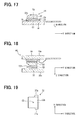
- FIG. 16 is a sectional view illustrating the method for manufacturing the semiconductor device according to the second embodiment
- FIG. 17 is a sectional view illustrating the method for manufacturing the semiconductor device according to the second embodiment.
- FIG. 18 is a sectional view illustrating the method for manufacturing the semiconductor device according to the second embodiment.
- FIG. 19 is a plan view illustrating a schematic configuration of a terminal in a semiconductor device according to a third embodiment
- FIG. 20 is a side view illustrating the schematic configuration of the terminal
- FIG. 21 is a sectional view illustrating an effect of the semiconductor device according to the third embodiment and corresponds to FIG. 7 ;
- FIG. 22 is a sectional view illustrating an effect of a semiconductor device according to a fourth embodiment and corresponds to FIG. 7 ;
- FIG. 23 is a sectional view illustrating a fourth modification and corresponds to FIG. 7 ;
- FIG. 24 is a sectional view illustrating an effect of a semiconductor device according to a fifth embodiment and corresponds to FIG. 7 ;
- FIG. 25 is a sectional view illustrating a fifth modification and corresponds to FIG. 7 ;
- FIG. 26 is a sectional view illustrating an effect of a semiconductor device according to a sixth embodiment and corresponds to FIG. 7 ;
- FIG. 27 is a sectional view illustrating a sixth modification and corresponds to FIG. 7 ;
- FIG. 28 is a plan view illustrating a schematic configuration of a semiconductor element in a semiconductor device according to a seventh embodiment and corresponds to FIG. 3 ;
- FIG. 29 is a sectional view illustrating an effect of the semiconductor device and corresponds to FIG. 4 ;
- FIG. 30 is a plan view illustrating a schematic configuration of a semiconductor element in a semiconductor device according to an eighth embodiment and corresponds to FIG. 3 ;
- FIG. 31 is a sectional view illustrating a schematic configuration of the semiconductor device according to the eighth embodiment.
- FIG. 32 is a diagram illustrating an arrangement of control pads when two semiconductor elements of the seventh embodiment are used.
- FIG. 33 is a diagram illustrating an arrangement of control pads when two semiconductor elements of the eighth embodiment are used.
- a stacking direction of a semiconductor element, a terminal, and each heat sink (described below) is referred to as a Z direction.
- An extending direction, which is perpendicular to the Z direction, of a terminal section and a control terminal is referred to as a Y direction.
- a direction perpendicular to both the Z direction and the Y direction is referred to as an X direction.
- An XY plane defined by the X direction and the Y direction is a plane perpendicular to the Z direction.
- a shape along the XY plane is referred to as a plane shape unless otherwise specified.
- the semiconductor device is known as a so-called 1-in-1 package.
- the semiconductor device is incorporated in an inverter circuit of a vehicle and applied as a device for PWM controlling a load.
- a semiconductor device 10 is provided with two semiconductor elements 12 , 14 .
- the semiconductor element 12 includes a semiconductor chip and an insulated gate bipolar transistor (IGBT) formed on the semiconductor chip.
- IGBT insulated gate bipolar transistor
- an N-channel IGBT is formed as an example.
- the semiconductor element 14 includes a semiconductor chip and a freewheeling diode (FWD) formed on the semiconductor chip.
- the freewheeling diode is also called a reflux diode.
- the semiconductor element 12 corresponds to a semiconductor element.
- Each of the semiconductor elements 12 , 14 has a so-called vertical structure so that current flows in the Z direction and has electrodes on both faces in the Z direction.
- the semiconductor element 12 includes an emitter electrode, a gate electrode, and control pads on a first face 12 a which faces a terminal 22 and has a collector electrode on a rear face 12 b which is located opposite to the first face 12 a .
- the semiconductor element 14 includes an anode electrode at the same side as the first face 12 a and has a cathode electrode at the same side as the rear face 12 b.
- These semiconductor elements 12 , 14 are disposed side by side in the X direction and disposed at substantially the same position in the Z direction.
- the plane shape of each of the semiconductor elements 12 , 14 is a substantially rectangular shape.
- the collector electrode is formed on substantially the entire rear face 12 b of the semiconductor element 12 and electrically, thermally, and mechanically connected to a first heat sink 18 through a solder 16 . That is, the collector electrode of the semiconductor element 12 and the first heat sink 18 are joined together with the solder 16 .
- the cathode electrode is also electrically, thermally, and mechanically connected to the first heat sink 18 through a solder (not illustrated).
- the solder 16 corresponds to a second solder
- the first heat sink 18 corresponds to a second metal member.
- the first heat sink 18 has a function of dissipating heat generated by the semiconductor elements 12 , 14 to the outside of the semiconductor device 10 .
- the first heat sink 18 is formed of at least a metal material.
- the first heat sink 18 is formed of a metal material having an excellent thermal conductivity and an excellent electrical conductivity such as copper, a copper alloy, and an aluminum alloy.
- a region in a facing face which faces the semiconductor elements 12 , 14 , the region having no solder 16 , and a side face are covered with a sealing resin body 34 (described below).
- a face located opposite to the facing face constitutes a heat dissipation surface 18 a which is exposed from a first face 34 a of the sealing resin body 34 .
- the first heat sink 18 includes a terminal section 18 b which serves as both a collector terminal of the IGBT of the semiconductor element 12 and a cathode terminal of the FWD of the semiconductor element 14 . As illustrated in FIG. 1 , the terminal section 18 b extends in the Y direction. A part of the terminal section 18 b projects to the outside from one side face 34 c of the sealing resin body 34 . In this manner, the terminal section 18 b can be electrically connected to an external device.
- the emitter electrode is formed on a part of the first face 12 a of the semiconductor element 12 and electrically, thermally, and mechanically connected to the terminal 22 through a solder 20 . That is, the emitter electrode of the semiconductor element 12 and the terminal 22 are joined together with the solder 20 . In the same manner, an anode electrode of the semiconductor element 14 is also electrically, thermally, and mechanically connected to a terminal 24 indicated by a broken line in FIG. 1 through a solder (not illustrated). In the present embodiment, the solder 20 corresponds to a first solder, and the terminal 22 is connected to a first metal member.
- each of the terminals 22 , 24 is located on the middle of a thermal and electrical conductive path between a second heat sink 32 (described below) and each of the semiconductor elements 12 , 14 .
- each of the terminals 22 , 24 is formed using at least a metal member to ensure thermal conductivity and electrical conductivity.
- each of the terminals 22 , 24 is formed of a metal material having an excellent thermal conductivity and an excellent electrical conductivity such as copper and molybdenum.
- Control pads are formed on the first face 12 a of the semiconductor element 12 in a part of an outer peripheral region excepting a region in which the emitter electrode is formed.
- Control terminals 28 are electrically connected to the respective control pads through bonding wires 26 . As illustrated in FIG. 1 , the control terminals 28 extend in the Y direction. A part of each of the control terminals 28 extends to the outside from one side face 34 c of the sealing resin body 34 at a side opposite to the side at which the terminal section 18 b projects. In this manner, the control terminals 28 can be electrically connected to an external device.
- the second heat sink 32 is electrically, thermally, and mechanically connected to a rear face 22 b of the terminal 22 , the rear face 22 b being located opposite to a facing face 22 a which faces the semiconductor element 12 , through a solder 30 .
- the terminal 24 corresponding to the semiconductor element 14 is also connected to the second heat sink 32 through a solder.
- the second heat sink 32 has a function of dissipating heat generated by the semiconductor elements 12 , 14 to the outside of the semiconductor device 10 similarly to the first heat sink 18 .
- the solder 30 corresponds to a third solder
- the second heat sink 32 corresponds to a third metal member.
- the second heat sink 32 is formed using at least a metal material to ensure thermal conductivity and electrical conductivity similarly to the first heat sink 18 .
- the second heat sink 32 is formed of a metal material having an excellent thermal conductivity and an excellent electrical conductivity such as copper, a copper alloy, and an aluminum alloy.
- a region in a facing face which faces the terminals 22 , 24 , the region having no solder 30 , and a side face are covered with the sealing resin body 34 .
- a face opposite to the facing face constitutes a heat dissipation surface 32 a which is exposed from a rear face 34 b of the sealing resin body 34 , the rear face 34 b being located opposite to the first face 34 a.
- the second heat sink 32 includes a terminal section 32 b which serves as both an emitter terminal of the semiconductor element 12 and an anode terminal of the semiconductor element 14 .
- the terminal section 32 b extends in the Y direction at a position displaced from the control terminals 28 in the X direction.
- a part of the terminal section 32 b projects to the outside from the side face 34 c of the sealing resin body 34 at a side opposite to the side at which the control terminals 28 project. In this manner, the terminal section 32 b can be electrically connected to an external device.
- the semiconductor elements 12 , 14 , a part of the first heat sink 18 , the terminals 22 , 24 , a part of each of the control terminals 28 , the bonding wires 26 , the solders 16 , 20 , 30 , and a part of the second heat sink 32 are sealed with the sealing resin body 34 .
- the sealing resin body 34 is molded by injecting a resin into a metal mold and has a substantially rectangular plane shape.
- an epoxy resin may be employed as the resin.
- the heat dissipation surface 18 a of the first heat sink 18 is exposed from the first face 34 a of the sealing resin body 34 .
- the heat dissipation surface 18 a is flush with the first face 34 a .
- the heat dissipation surface 32 a of the second heat sink 32 is exposed from the rear face 34 b located opposite to the first face 34 a .
- the heat dissipation surface 32 a is flush with the rear face 34 b .
- the control terminals 28 project from the side face 34 c at one side.
- Each of the terminal sections 18 b , 32 b projects from the side face 34 c at a side opposite to the side at which the control terminals 28 project.
- the semiconductor element 12 and the terminal 22 will be described in detail with reference to FIGS. 3 and 4 .
- the bonding wires 26 and the sealing resin body 34 are omitted for the sake of convenience.
- the semiconductor element 12 includes the emitter electrode 36 on the first face 12 a .
- the semiconductor element 12 also includes the control pads 40 in the outer peripheral region 38 which surrounds the emitter electrode 36 .
- the emitter electrode 36 has a rectangular plane shape and includes an element center C 1 which is the center of the semiconductor element 12 within the XY plane.
- substantially the entire emitter electrode 36 constitutes a solder region 12 a 1 which is connected to the terminal 22 through the solder 20 .
- a region excepting the solder region 12 a 1 constitutes a non-solder region 12 a 2 which is not connected to the solder 20 . That is, the non-solder region 12 a 2 includes at least the outer peripheral region 38 .
- the control pads 40 correspond to external connection pads.
- the control pads 40 include temperature sense pads 40 a , 40 b , a gate electrode pad 40 c , a current sense pad 40 d , and a Kelvin emitter pad 40 e .
- These control pads 40 ( 40 a to 40 e ) are formed side by side in the X direction in the outer peripheral region 38 at one end side in the Y direction.
- the outer peripheral region 38 is wider at the side having the control pads 40 . Accordingly, a center C 2 of the solder region 12 a 1 is displaced in the Y direction with respect to the element center C 1 .
- the terminal 22 is formed by cutting away a part of a substantially rectangular parallelepiped.
- the facing face 22 a of the terminal 22 is flat and has a rectangular plane shape which substantially coincides with the emitter electrode 36 . That is, a terminal center C 3 substantially coincides with the center C 2 of the solder region 12 a 1 within the XY plane.
- the rear face 22 b has the same rectangular plane shape as the facing face 22 a . However, the rear face 22 b is not flat in the entire area and has a cut portion 22 c.
- the cut portion 22 c is a region located opposite to the control pads 40 in the Y direction and formed at a position away from the terminal center C 3 .
- the cut portion 22 c is formed on the entire area in the X direction.
- a part of the rear face 22 b in which the cut portion 22 c is formed forms an inclined plane whose distance to the facing face 22 a in the Z direction is reduced toward a direction away from the terminal center C 3 in the Y direction.
- the remaining part of the rear face 22 b forms a flat plane substantially parallel to the facing face 22 a.
- the cut portion 22 c is formed so that a terminal gravity center Cg comes closer to the element center C 1 of the semiconductor element 12 within the XY plane when the first heat sink 18 , the semiconductor element 12 , and the terminal 22 are connected through the solders 16 , 20 . Accordingly, the weight distribution of the terminal 22 is biased.
- the cut portion 22 c is formed so that the terminal gravity center Cg coincides with the element center C 1 .
- the cut portion 22 c is formed so that the terminal gravity center Cg coincides with the element center C 1 in a projection view from the Z direction.
- the coincidence between the terminal gravity center Cg and the element center C 1 is not limited to exact coincidence, and may be substantial coincidence. It is only required that the terminal gravity center Cg be located closer to the element center C 1 than the terminal center C 3 .
- the second heat sink 32 is substantially parallel to a flat part of the rear face 22 b of the terminal 22 excepting the cut portion 22 c .
- the solder 30 is thicker in a part corresponding to the cut portion 22 c than a part corresponding to the flat part excepting the cut portion 22 c.
- the anode electrode is formed on substantially the entire first face of the semiconductor element 14 .
- the terminal 24 has no cut portion and has a substantially rectangular parallelepiped shape.
- the semiconductor elements 12 , 14 , the heat sinks 18 , 32 , the terminals 22 , 24 , and the control terminals 28 are prepared.
- the terminal 22 having the cut portion 22 c is prepared.
- the cut portion 22 c may be formed, for example, when the terminal 22 is formed by punching out a metal plate.
- a preliminary soldering step is performed.
- the solder 30 is disposed inside a container 42 which is formed using, for example, carbon, and the terminal 22 is disposed on the solder 30 with the rear face 22 b facing down.
- the solder 20 is disposed so as to cover the terminal 22 . Accordingly, the solder 20 for preliminary soldering is applied to the facing face 22 a of the terminal 22 , and the solder 30 for preliminary soldering is applied to the rear face 22 b so as to cover the cut portion 22 c .
- the solders 20 , 30 in a molten state may be disposed inside the container 42 , or the solders 20 , 30 may be molten after disposed inside the container 42 .
- preliminary soldering is applied also to both the faces of the terminal 24 .
- a first reflow step is performed.
- the semiconductor element 12 is stacked on the first heat sink 18 with the solder 16 (for example, a solder foil) interposed therebetween, and the terminal 22 is stacked on the semiconductor element 12 with the solder 20 facing the semiconductor element 12 .
- the solders 16 , 20 , 30 are reflowed to form a connection body 44 which includes the first heat sink 18 the semiconductor element 12 , and the terminal 22 integrated together as illustrated in FIG. 7 .
- solders 16 , 20 are simultaneously reflowed in the stacked state to join the semiconductor element 12 and the first heat sink 18 together with the molten solder 16 and to join the terminal 22 and the semiconductor element 12 together with the molten solder 20 . That is, in the stacked state, the solders 16 , 20 provide reflow joining as melt-joining.
- the terminal 22 has the cut portion 22 c , and the terminal 22 is disposed on the semiconductor element 12 in a manner to align the facing face 22 a with the solder region 12 a 1 . Accordingly, the terminal gravity center Cg substantially coincides with the element center C 1 in the projection view from the Z direction. In this manner, the first reflow step is performed with the terminal gravity center Cg substantially coincident with the element center C 1 . In the first reflow step, a positioning jig may be used so as to align the facing face 22 a with the solder region 12 a 1 .
- the solder 30 Since the second heat sink 32 as a connection target has not yet been connected to the solder 30 , the solder 30 has a swollen shape with the apex corresponding to the center of the terminal 22 due to surface tension.
- the semiconductor element 14 is soldered to the first heat sink 18 , and the terminal 24 is soldered to the semiconductor element 14 .
- a wire bonding step is performed.
- the control terminals 28 are connected to the respective control pads 40 of the semiconductor element 12 with the bonding wires 26 .
- a second reflow step is performed.
- the second heat sink 32 is disposed on a mount (not illustrated).
- the connection body 44 is disposed on the second heat sink 32 with the solder 30 facing the second heat sink 32 .
- the solder 30 is reflowed while applying pressure from the first heat sink 18 in the Z direction.
- one end of a spacer (not illustrated) is fixed to the mount. The pressure is applied from the first heat sink 18 so as to bring the face of the first heat sink 18 , the face being located opposite to the heat dissipation surface 18 a , into contact with the other end of the spacer. That is, the spacer adjusts the distance between the heat dissipation surfaces 18 a , 32 a .
- a heater disposed on the mount heats the second heat sink 32 to melt only the solder 30 .
- the second heat sink 32 and the terminal 22 are connected to each other through the solder 30 .
- the terminal 24 and the second heat sink 32 are also connected to each other.
- a molding step of molding the sealing resin body 34 is performed.
- the connection structure obtained in the second reflow step is disposed in a metal mold (not illustrated), and a resin is injected into a cavity of the metal mold to mold the sealing resin body 34 .
- the sealing resin body 34 is molded by a transfer mold method using an epoxy resin. Since the heat dissipation surface 18 a of the heat sink 18 and the heat dissipation surface 32 a of the heat sink 32 are cut in a cutting step (described below), the sealing resin body 34 is molded in such a manner that at least either the heat sink 18 or the heat sink 32 is not exposed from the sealing resin body 34 .
- the cutting step is performed.
- the first heat sink 18 is cut with a cutting tool (not illustrated) together with the sealing resin body 34 from the first face 34 a of the sealing resin body 34 .
- the cutting exposes only the heat dissipation surface 18 a from the sealing resin body 34 in the first heat sink 18 and makes the heat dissipation surface 18 a substantially flush with the first face 34 a .
- the second heat sink 32 is cut together with the sealing resin body 34 from the rear face 34 b of the sealing resin body 34 .
- the cutting exposes only the heat dissipation surface 32 a from the sealing resin body 34 in the second heat sink 32 and makes the heat dissipation surface 32 a flush with the rear face 34 b .
- the cutting on both the faces makes it possible to ensure the flatness of the heat dissipation surfaces 18 a , 32 a and the parallelism between the heat dissipation surfaces 18 a , 32 a.
- a tie bar of a lead frame (not illustrated) is removed to obtain the semiconductor device 10 .
- the removal of the unnecessary part may be performed before the cutting step.
- a terminal 122 has a substantially rectangular parallelepiped shape, and a terminal gravity center Cgr coincides with a terminal center C 3 r within the XY plane. That is, the terminal gravity center Cgr is displaced from an element center C 1 r in a projection view from the Z direction.
- the weight of the terminal 122 acting on a semiconductor element 112 is larger at the terminal gravity center Cgr than the element center C 1 r in the Y direction, which causes the tilt of the semiconductor element 112 .
- FIG. 11 illustrates a first heat sink 118 , a control terminal 128 , and a solder 130 .
- the terminal gravity center Cg is located closer to the element center C 1 than the terminal center C 3 within the XY plane.
- SAT scanning acoustic tomograph
- the cut portion 22 c is formed so that the terminal gravity center Cg coincides with the element center C 1 .
- the tilt of the semiconductor element 12 can be more effectively reduced.
- the occurrence of the tilt of the semiconductor element 12 can be reduced in the present embodiment.
- the bonding wires 26 are easily ultrasonic-bonded to the control pads 40 of the semiconductor element 12 .
- the cut portion 22 c can be formed, for example, simultaneously with the punching-out of the terminal 22 .
- the configuration of the terminal 22 can be simplified.
- the cut portion 22 c is formed on the rear face 22 b of the terminal 22 . Accordingly, the thickness of the solder 20 between the semiconductor element 12 and the terminal 22 is substantially uniform. Thus, it is possible to further improve the heat dissipation from the semiconductor element 12 to the second heat sink 32 compared with a configuration that has a cut portion formed on the facing face 22 a located close to the semiconductor element 12 , that is, close to a heat generation source.
- a cut portion 22 c is formed as a V-shaped groove. Such a cut portion 22 c can be formed by striking the terminal 22 from the rear face 22 b.
- a part of the rear face 12 b within a predetermined range is uniformly recessed by a predetermined depth in the Z direction to form a cut portion 22 c .
- the cut portion 22 c is formed from an end opposite to the control pads 40 across the terminal gravity center Cg.
- the entire rear face 22 b forms an inclined plane. Accordingly, the terminal 22 has a partially different thickness. Specifically, the terminal 22 becomes thicker toward the control pads 40 in the Y direction.
- a flat part excepting the cut portion 22 c is narrower than the cut portion 22 c .
- the entire rear face 22 b forms the inclined plane.
- the flat part excepting the cut portion 22 c may be wider than the cut portion 22 c . This improves an effect of reducing the tilt when the solders 16 , 20 are also molten in the second reflow step. As described above, when only the solder 30 is molten in the second reflow step, the tilt of the terminal 22 can be reduced regardless of the presence or absence of the flat part of the terminal 22 .
- terminals 22 illustrated in FIGS. 4 and 12 can be formed by punching-out or striking, the manufacture of the terminals 22 illustrated in FIGS. 4 and 12 is easier than the manufacture of the terminals 22 illustrated in FIGS. 13 and 14 .
- the solders 20 , 30 for preliminary soldering are applied to both the faces 22 a , 22 b of the terminal 22 in the preliminary soldering step.
- the solder 30 for preliminary soldering is applied so as to cover the cut portion 22 c .
- the metal material constituting the terminal 22 (for example, copper) has a larger specific gravity than the solder 30 .
- the terminal gravity center Cg comes closer to the element center C 1 than the terminal center C 3 within the XY plane.
- the effect is reduced by the solder 30 .
- solder 20 for preliminary soldering is applied to a terminal 22 in a preliminary soldering step as illustrated in FIG. 15 . That is, no solder 30 for preliminary soldering is applied to the rear face 22 b.
- a semiconductor element 12 is stacked on a first heat sink 18 with a solder 16 interposed therebetween.
- the terminal 22 with only the solder 20 applied thereto is stacked on the semiconductor element 12 with the solder 20 facing the semiconductor element 12 .
- the solders 16 , 20 are reflowed to form a connection body 44 which includes the first heat sink 18 , the semiconductor element 12 , and the terminal 22 integrated together as illustrated in FIG. 17 .
- no solder 30 is applied to the terminal 22 .
- a terminal gravity center Cg but also the gravity center of the terminal 22 including the solder 20 substantially coincides with an element center C 1 in a projection view from the Z direction.
- a wire bonding step and a second reflow step are sequentially performed after the first reflow step similarly to the first embodiment.
- a second heat sink 32 is disposed on a mount (not illustrated).
- a solder 30 for example, a solder foil
- the connection body 44 are disposed in this order on the second heat sink 32 .
- the solder 30 is reflowed while applying pressure from the first heat sink 18 in the Z direction.
- a molding step and a cutting step are performed after the second reflow step similarly to the first embodiment. Accordingly, the semiconductor device 10 described in the first embodiment can be obtained.
- the solder 20 for preliminary soldering is applied to the terminal 22 in the preliminary soldering step.
- the gravity center of the terminal 22 including the solder 20 substantially coincides with the element center C 1 in the projection view from the Z direction in the first reflow.
- a terminal 22 has projections 22 e which project from side faces 22 d adjacent to both a facing face 22 a and a rear face 22 b as illustrated in FIGS. 19 and 20 .
- Each of the projections 2 e is formed on the corresponding side face 22 d at a position away from the facing face 22 a in the Z direction.
- the projections 22 e are formed in regions between a terminal center C 3 and the control pads 40 .
- the terminal 22 is line-symmetric with respect to a virtual line that passes through the terminal center C 3 along the Y direction.
- the projections 22 e are flush with the rear face 22 b.
- the present embodiment makes it possible to reduce the occurrence of the tilt of the semiconductor element 12 in the first reflow step similarly to the first embodiment.
- the projections 22 e which project from the side faces 22 d are formed on the terminal 22 to achieve a partially different thickness of the terminal 22 to bring a terminal gravity center Cg close to the element center C 1 in a projection view from the Z direction. Further, the terminal gravity center Cg is brought into coincidence with the element center C 1 .
- the thickness of each of the solders 20 , 30 can be made substantially uniform within the XY plane. Accordingly, it is possible to improve the heat dissipation from the semiconductor element 12 to the second heat sink 32 .
- both the facing face 22 a and the rear face 22 b are flat.
- the projections 22 e are formed at the positions away from the facing face 22 a , it is possible to reduce adhesion of the solder 20 to the projections 22 e . Accordingly, the solder 20 is connected to the terminal 22 only on the facing face 22 a , which enables the heat dissipation to be improved.
- a terminal 22 has a cavity 22 f which is open on side faces 22 d as illustrated in FIG. 22 .
- the cavity 22 f is formed in a region located opposite to the control pads 40 with respect to a terminal center C 3 and penetrates the opposite side faces 22 d .
- the cavity 22 f may be formed by machining such as drilling.
- the cavity 22 f which is open on the side faces 22 d is formed on the terminal 22 to achieve a partially different thickness of the terminal 22 to bring a terminal gravity center Cg close to the element center C 1 in a projection view from the Z direction. Further, the terminal gravity center Cg is brought into coincidence with the element center C 1 .
- forming the cavity 22 f makes both a facing face 22 a and a rear face 22 b flat.
- a cavity 22 f is not limited to the above example.
- a cavity 22 f is a groove which is formed across three adjacent side faces 22 d.
- the material constituting a terminal 22 has a partially different density within the XY plane.
- the terminal 22 has a low density part 22 g which is a base material itself of the terminal 22 and a high density part 22 h which is formed by mixing a material having a higher density than the base material with the base material.
- a half of the terminal 22 located at a side corresponding to the control pads 40 constitutes the high density part 22 h
- the other half thereof constitutes the low density part 22 g.
- the terminal 22 has the partially different density to bring a terminal gravity center Cg close to the element center C 1 in a projection view from the Z direction. Further, the terminal gravity center Cg is brought into coincidence with the element center C 1 . Thus, it is possible to reduce the occurrence of the tilt of the semiconductor element 12 in the first reflow step similarly to the first embodiment.
- both a facing face 22 a and a rear face 22 b are flat.
- the solders 16 , 20 are molten in the second reflow step, it is possible to reduce the tilt of the terminal 22 with respect to the XY plane and, in addition, the tilt of the semiconductor element 12 caused by the tilt of the terminal 22 .
- a method for achieving the difference in density is not limited to the above example.
- a plating 22 i is applied to a part of the surface of the terminal 22 at a side corresponding to the control pads 40 .
- a material having a higher density than the material of the terminal 22 may be used as the plating 22 i . Accordingly, it is possible to make the part with the plating 22 i heavier than a part without the plating 22 i . As a result, it is possible to bring the terminal gravity center Cg close to the element center C 1 in a projection view from the Z direction and, further, bring the terminal gravity center Cg into coincidence with the element center C 1 .
- the surface of the low density part 22 g and the surface of the high density part 22 h may be plated, and a plating material on the high density part 22 h may have a higher density than a plating material on the low density part 22 g.
- a terminal 22 includes a plurality of members.
- the terminal 22 includes two members 22 j , 22 k . Both the first member 22 j and the second member 22 k are formed using the same material and integrated together by joining.
- the second member 22 k which is located at a side corresponding to the control pads 40 in the Y direction is higher than the first member 22 j in the Z direction.
- the terminal 22 includes the plurality of members 22 j , 22 k , and the members 22 j , 22 k differ in height to bring a terminal gravity center Cg close to the element center C 1 in a projection view from the Z direction. Further, the terminal gravity center Cg is brought into coincidence with the element center C 1 .
- This configuration also makes it possible to achieve an effect similar to the effect of the first embodiment.
- the configuration including a plurality of members is not limited to the above example.
- the constituent material of the first member 22 j and the constituent material of the second member 22 k may differ in density.
- the surface of the second member 22 k may be plated.
- a first member 22 j and a second member 22 k which constitute a terminal 22 may be separated from each other.
- the cut portion 22 c is formed on the terminal 22 to bring the terminal gravity center Cg into coincidence with the element center C 1 in the projection view from the 1 direction.
- a solder region 12 a 1 and non-solder regions 12 a 2 of a semiconductor element 12 are divided so that a center C 2 of the solder region 12 a 1 coincides with an element center C 1 within the XY plane as illustrated in FIG. 28 . That is, adjustment is performed on the semiconductor element 12 so that the terminal gravity center Cg coincides with the element center C 1 .
- the arrangement of an emitter electrode 36 and an outer peripheral region 38 is the same as that in the first embodiment.
- the seventh embodiment differs from the first embodiment in that not the entire emitter electrode 36 , but only a part of the emitter electrode 36 located closer to the control pads 40 in the Y direction is defined as the solder region 12 a 1 indicated by a broken line which is soldered to the terminal 22 .
- the vicinity of an end located opposite to the control pads 40 in the Y direction constitutes the non-solder region 12 a 2 .
- the non-solder regions 12 a 2 are formed with the solder region 12 a 1 interposed therebetween in the Y direction.
- the non-solder regions 12 a 2 on both sides have substantially the same length in the Y direction.
- the part of the emitter electrode 36 located opposite to the control pads 40 is defined as the non-solder region 12 a 2 . Accordingly, as illustrated in FIG. 29 , the center C 2 of the solder region 12 a 1 is brought into coincidence with the element center C 1 and, further, coincidence with the terminal gravity center Cg in a projection view from the Z direction.
- the terminal 22 has a substantially rectangular parallelepiped shape, and the terminal center C 3 coincides with the terminal gravity center Cg. This configuration also makes it possible to achieve an effect similar to the effect of the first embodiment.
- FIG. 29 corresponds to FIG. 4 and omits the sealing resin body 34 and the bonding wires 26 similarly to FIG. 4 .
- control pads 40 are disposed in one of the non-solder regions 12 a 2 which are formed with the solder region 12 a 1 interposed therebetween in the Y direction.
- the same kinds and same number of control pads 40 are disposed on non-solder regions 12 a 2 (outer peripheral region 38 ) located on both sides in the Y directions as illustrated in FIG. 30 .
- the control pads 40 in each of the non-solder regions 12 a 2 are formed in the same order in the X direction.
- the Y direction corresponds to a first direction
- the X direction corresponds to a second direction.
- one of the non-solder regions 12 a 2 is located on one end side of the solder region 12 a 1
- the other non-solder region 12 a 2 is located on the other end side of the solder region 12 a 1 .
- the plurality of kinds of control pads 40 are disposed in the non-solder region 12 a 2 on one end side.
- the same kinds and same number of control pads 40 as the control pads 40 in the non-solder region 12 a 2 on one end side are disposed in the non-solder region 12 a 2 on the other end side.
- the plurality of kinds of control pads 40 are formed in a predetermined order along the X direction.
- the control pads 40 are formed in the same order as the control pads 40 formed in the non-solder region 12 a 2 on one end side along the X direction.
- a temperature sense pad 40 a cathode
- a temperature sense pad 40 b anode
- a gate electrode pad 40 c a current sense pad 40 d
- a Kelvin emitter pad 40 e are formed as the control pads 40 in each of the non-solder regions 12 a 2 on one and the other end sides.
- the temperature sense pad 40 a , the temperature sense pad 40 b , the gate electrode pad 40 c , the current sense pad 40 d , and the Kelvin emitter pad 40 e are formed in this order from the left side of the drawing.
- a semiconductor device 10 includes two semiconductor elements 12 (IGBTs) connected in series, that is, a pair of upper and lower arms.
- the semiconductor device 10 includes a high potential power terminal 46 (so-called P terminal) which is connected to a high potential side of a DC power supply, a low potential power terminal 48 (so-called N terminal) which is connected to a low potential side of the DC power supply, and an output terminal 50 (so-called O terminal).
- the semiconductor device 10 includes an upper arm side semiconductor element 12 U and a lower arm side semiconductor element 12 L as the semiconductor elements 12 .
- the sealing resin body 34 is omitted for the sake of convenience.
- the upper arm side semiconductor element 12 U is disposed between the high potential power terminal 46 and the output terminal 50 with a collector electrode facing the high potential power terminal 46 .
- the collector electrode of the semiconductor element 12 U is connected to the high potential power terminal 46 through a solder 16 .
- An emitter electrode 36 of the semiconductor element 12 U is electrically connected to the output terminal 50 through a solder 20 , a terminal 22 , and a solder 30 .
- the lower arm side semiconductor element 12 L is disposed between the low potential power terminal 48 and the output terminal 50 with a collector electrode facing the output terminal 50 .
- the collector electrode of the semiconductor element 12 L is connected to the output terminal 50 through a solder 16 .
- An emitter electrode 36 of the semiconductor element 12 L is electrically connected to the low potential power terminal 48 through a solder 20 , a terminal 22 , and a solder 30 .
- the output terminal 50 is common between the semiconductor elements 12 U, 12 L, and the semiconductor element 12 U is disposed upside down in the Z direction with respect to the semiconductor element 12 L.
- the semiconductor element 12 U is disposed with a first face 12 a facing the output terminal 50 .
- the semiconductor element 12 L is disposed with a rear face 12 b facing the output terminal 50 .
- the semiconductor device 10 is a so-called U-shaped 2-in-1 package.
- the terminal 22 corresponds to the first metal member
- the high potential power terminal 46 corresponds to the second metal member
- the output terminal 50 corresponds to the third metal member
- the terminal 22 corresponds to the first metal member
- the output terminal 50 corresponds to the second metal member
- the low potential power terminal 48 corresponds to the third metal member.
- Each of the semiconductor elements 12 U, 12 L has the structure illustrated in FIG. 30 .
- control pads 40 are formed only in one of the non-solder regions 12 a 2 and the semiconductor element 12 U is disposed upside down with respect to the semiconductor element 12 L to employ the U-shaped 2-in-1 package structure, the order of the control pads 40 is opposite between the semiconductor elements 12 U, 12 L as illustrated in FIG. 32 .
- the high potential power terminal 46 and the low potential power terminal 48 are omitted.
- the control pads 40 are disposed in the non-solder regions 12 a 2 on both sides in the same order as illustrated in FIG. 31 .
- the semiconductor elements 12 U is disposed upside down with respect to the semiconductor element 12 L, and one of the semiconductor elements 12 U, 12 L is turned by 180° with respect to the other.
- the order of the control pads 40 is the same between the upper arm side semiconductor element 12 U and the lower arm side semiconductor element 12 L.
- the connection structure between an external device and the control terminals 28 can be simplified.
- the high potential power terminal 46 and the low potential power terminal 48 are omitted.
- the semiconductor device 10 includes the terminal 22 .
- a configuration that includes no terminal 22 may be employed.
- the second heat sink 32 is connected to the semiconductor element 12 through the solder 20 . That is, the second heat sink 32 corresponds to the first metal member.
- the semiconductor device 10 includes the second heat sink 32 .
- a configuration that includes no second heat sink 32 may be employed.
- a configuration that includes no second heat sink 32 and no solder 30 may be employed.
- examples of the 1-in-1 package and the U-shaped 2-in-1 package have been described as the semiconductor device 10 .
- the present disclosure may also be applied to other configurations, for example, an N-shaped 2-in-1 package and a 6-in-1 package.
- the N-shaped 2-in-1 package also has a pair of upper and lower arms.
- the placement of the upper arm side semiconductor element 12 U and the placement of the lower arm side semiconductor element 12 L are the same in the Z direction.
- Separate output terminals 50 are provided for the respective semiconductor elements 12 U, 12 L.
- One of the output terminals 50 is disposed on a first face 34 a of a sealing resin body 34
- the other output terminal 50 is disposed on a rear face 34 b of the sealing resin body 34 .
- the output terminals 50 are electrically connected to each other through a joint section. Either a high potential power terminal 46 or a low potential power terminal 48 is disposed on the first face 34 a , and the other one is disposed on the rear face 34 b .
- the structure for electrically connecting the high potential power terminal 46 , the output terminals 50 , and the low potential power terminal 48 has an N shape.
- the 6-in-1 package includes three pairs of upper and lower arms. That is, the 6-in-1 package has semiconductor elements 12 for three phases.
- the configuration that brings the gravity center position Cg of the terminal 22 into coincidence with the center position C 1 of the semiconductor element 12 in the projection view from the Z direction is applied to the semiconductor device 10 that is formed by reflowing both the solders 16 , 20 with the semiconductor element 12 stacked on the first heat sink 18 with the solder 16 interposed therebetween and the terminal 22 stacked on the semiconductor element 12 with the solder 20 interposed therebetween.
- the above configuration may be applied to a semiconductor device 10 formed by a method other than reflow.
- the semiconductor element may be tilted.
- the above configuration may be applied to a semiconductor device 10 in which at least the solder 16 , among the solders 16 , 20 , provides melt-joining in the stacked state.
- the above configuration may be applied to a semiconductor device 10 that is manufactured in such a manner that a semiconductor element 12 is stacked on a first heat sink 18 with a molten solder 16 interposed therebetween, a terminal 22 is stacked on the semiconductor element 12 with a molten solder 20 interposed therebetween, and both the molten solders 16 , 20 are cooled and solidified in the stacked state. Also in such a semiconductor device 10 , both the solders 16 , 20 are molten in the stacked state.
- it is possible to reduce the occurrence of the tilt of the semiconductor element 12 by bringing the gravity center position Cg of the terminal 22 into coincidence with the center position C 1 of the semiconductor element 12 in the projection view from the Z direction.
- the above configuration may be applied to a semiconductor device 10 that is manufactured in such a manner that a semiconductor element 12 and a terminal 22 are previously joined together with a solder 20 , the semiconductor element 12 with the terminal 22 joined thereto is then stacked on a first heat sink 18 with a molten solder 16 interposed therebetween, and the molten solder 16 is cooled and solidified in the stacked state. That is, the above configuration may also be applied to a semiconductor device 10 in which only the solder 16 , among the solders 16 , 20 , provides melt-joining in the stacked state. Also in this case, it is possible to reduce the occurrence of the tilt of the semiconductor element 12 by bringing the gravity center position Cg of the terminal 22 into coincidence with the center position C 1 of the semiconductor element 12 in the projection view from the Z direction.
Landscapes
- Engineering & Computer Science (AREA)
- Computer Hardware Design (AREA)
- Microelectronics & Electronic Packaging (AREA)
- Power Engineering (AREA)
- Physics & Mathematics (AREA)
- Condensed Matter Physics & Semiconductors (AREA)
- General Physics & Mathematics (AREA)
- Mechanical Engineering (AREA)
- Chemical & Material Sciences (AREA)
- Materials Engineering (AREA)
- Cooling Or The Like Of Semiconductors Or Solid State Devices (AREA)
Applications Claiming Priority (5)
| Application Number | Priority Date | Filing Date | Title |
|---|---|---|---|
| JP2014-007530 | 2014-01-20 | ||
| JP2014007530 | 2014-01-20 | ||
| JP2014-249164 | 2014-12-09 | ||
| JP2014249164A JP6269458B2 (ja) | 2014-01-20 | 2014-12-09 | 半導体装置及びその製造方法 |
| PCT/JP2015/000072 WO2015107879A1 (ja) | 2014-01-20 | 2015-01-09 | 半導体装置及びその製造方法 |
Publications (2)
| Publication Number | Publication Date |
|---|---|
| US20160204047A1 US20160204047A1 (en) | 2016-07-14 |
| US9502327B2 true US9502327B2 (en) | 2016-11-22 |
Family
ID=53542776
Family Applications (1)
| Application Number | Title | Priority Date | Filing Date |
|---|---|---|---|
| US14/913,719 Active US9502327B2 (en) | 2014-01-20 | 2015-01-09 | Semiconductor device and method for manufacturing the same |
Country Status (3)
| Country | Link |
|---|---|
| US (1) | US9502327B2 (ja) |
| JP (1) | JP6269458B2 (ja) |
| WO (1) | WO2015107879A1 (ja) |
Cited By (1)
| Publication number | Priority date | Publication date | Assignee | Title |
|---|---|---|---|---|
| US20200058574A1 (en) * | 2018-08-15 | 2020-02-20 | Kabushiki Kaisha Toshiba | Semiconductor device and power convertor |
Families Citing this family (7)
| Publication number | Priority date | Publication date | Assignee | Title |
|---|---|---|---|---|
| JP6269458B2 (ja) * | 2014-01-20 | 2018-01-31 | 株式会社デンソー | 半導体装置及びその製造方法 |
| JP6551432B2 (ja) * | 2017-02-08 | 2019-07-31 | トヨタ自動車株式会社 | 半導体装置とその製造方法 |
| DE112017007960B4 (de) * | 2017-09-04 | 2023-06-29 | Mitsubishi Electric Corporation | Halbleitermodul und Leistungsumwandlungsvorrichtung |
| US10566267B2 (en) * | 2017-10-05 | 2020-02-18 | Texas Instruments Incorporated | Die attach surface copper layer with protective layer for microelectronic devices |
| JP6981192B2 (ja) * | 2017-11-15 | 2021-12-15 | トヨタ自動車株式会社 | 半導体装置の製造方法 |
| JP7120083B2 (ja) | 2019-03-06 | 2022-08-17 | 株式会社デンソー | 半導体装置 |
| JP2023139980A (ja) * | 2022-03-22 | 2023-10-04 | 株式会社東芝 | 半導体装置 |
Citations (8)
| Publication number | Priority date | Publication date | Assignee | Title |
|---|---|---|---|---|
| JP2002217364A (ja) | 2001-01-15 | 2002-08-02 | Nissan Motor Co Ltd | 半導体実装構造 |
| US20050056927A1 (en) | 2003-09-17 | 2005-03-17 | Takanori Teshima | Semiconductor device having a pair of heat sinks and method for manufacturing the same |
| US20050077617A1 (en) | 2003-10-09 | 2005-04-14 | Denso Corporation | Semiconductor device having heat radiation plate and bonding member |
| JP2005347684A (ja) | 2004-06-07 | 2005-12-15 | Nissan Motor Co Ltd | 半導体装置 |
| JP2008135613A (ja) | 2006-11-29 | 2008-06-12 | Denso Corp | 半導体装置の製造方法 |
| JP2008181908A (ja) | 2007-01-23 | 2008-08-07 | Rohm Co Ltd | 半導体装置及び半導体装置用リードフレーム |
| JP2012186273A (ja) | 2011-03-04 | 2012-09-27 | Denso Corp | 半導体装置、金属ブロック体及びその製造方法 |
| US20160204047A1 (en) * | 2014-01-20 | 2016-07-14 | Denso Corporation | Semiconductor device and method for manufacturing the same |
Family Cites Families (3)
| Publication number | Priority date | Publication date | Assignee | Title |
|---|---|---|---|---|
| JPH09232339A (ja) * | 1996-02-21 | 1997-09-05 | Sanken Electric Co Ltd | 半導体装置 |
| JP4339660B2 (ja) * | 2003-10-09 | 2009-10-07 | 株式会社デンソー | 半導体装置 |
| JP5512377B2 (ja) * | 2010-04-28 | 2014-06-04 | 本田技研工業株式会社 | 回路基板 |
-
2014
- 2014-12-09 JP JP2014249164A patent/JP6269458B2/ja not_active Expired - Fee Related
-
2015
- 2015-01-09 US US14/913,719 patent/US9502327B2/en active Active
- 2015-01-09 WO PCT/JP2015/000072 patent/WO2015107879A1/ja active Application Filing
Patent Citations (8)
| Publication number | Priority date | Publication date | Assignee | Title |
|---|---|---|---|---|
| JP2002217364A (ja) | 2001-01-15 | 2002-08-02 | Nissan Motor Co Ltd | 半導体実装構造 |
| US20050056927A1 (en) | 2003-09-17 | 2005-03-17 | Takanori Teshima | Semiconductor device having a pair of heat sinks and method for manufacturing the same |
| US20050077617A1 (en) | 2003-10-09 | 2005-04-14 | Denso Corporation | Semiconductor device having heat radiation plate and bonding member |
| JP2005347684A (ja) | 2004-06-07 | 2005-12-15 | Nissan Motor Co Ltd | 半導体装置 |
| JP2008135613A (ja) | 2006-11-29 | 2008-06-12 | Denso Corp | 半導体装置の製造方法 |
| JP2008181908A (ja) | 2007-01-23 | 2008-08-07 | Rohm Co Ltd | 半導体装置及び半導体装置用リードフレーム |
| JP2012186273A (ja) | 2011-03-04 | 2012-09-27 | Denso Corp | 半導体装置、金属ブロック体及びその製造方法 |
| US20160204047A1 (en) * | 2014-01-20 | 2016-07-14 | Denso Corporation | Semiconductor device and method for manufacturing the same |
Non-Patent Citations (2)
| Title |
|---|
| International Search Report of the International Searching Authority dated Apr. 7, 2015 issued in the corresponding International application No. PCT/JP2015/000072 (and English translation). |
| Written Opinion of the International Searching Authority dated Apr. 7, 2015 issued in the corresponding International application No. PCT/JP2015/000072 (and English translation). |
Cited By (2)
| Publication number | Priority date | Publication date | Assignee | Title |
|---|---|---|---|---|
| US20200058574A1 (en) * | 2018-08-15 | 2020-02-20 | Kabushiki Kaisha Toshiba | Semiconductor device and power convertor |
| US10811337B2 (en) * | 2018-08-15 | 2020-10-20 | Kabushiki Kaisha Toshiba | Semiconductor device and power convertor |
Also Published As
| Publication number | Publication date |
|---|---|
| JP6269458B2 (ja) | 2018-01-31 |
| US20160204047A1 (en) | 2016-07-14 |
| WO2015107879A1 (ja) | 2015-07-23 |
| JP2015156475A (ja) | 2015-08-27 |
Similar Documents
| Publication | Publication Date | Title |
|---|---|---|
| US9502327B2 (en) | Semiconductor device and method for manufacturing the same | |
| US9673118B2 (en) | Power module and method of manufacturing power module | |
| US9520345B2 (en) | Semiconductor module, semiconductor device having semiconductor module, and method of manufacturing semiconductor module | |
| US9224662B2 (en) | Semiconductor apparatus | |
| US20160035646A1 (en) | Semiconductor device, method for assembling semiconductor device, semiconductor device component, and unit module | |
| JP2015119072A (ja) | レーザ溶接方法、レーザ溶接治具、半導体装置 | |
| WO2018179981A1 (ja) | 半導体装置 | |
| WO2022080055A1 (ja) | 半導体モジュール | |
| JP6230238B2 (ja) | 半導体装置及びその製造方法 | |
| JP7354475B1 (ja) | 半導体モジュール | |
| JP7411849B2 (ja) | 半導体モジュール | |
| US9076782B2 (en) | Semiconductor device and method of manufacturing same | |
| US10497586B2 (en) | Semiconductor device and a method of manufacturing the same | |
| JP6155676B2 (ja) | 半導体装置及びその製造方法 | |
| KR101644913B1 (ko) | 초음파 용접을 이용한 반도체 패키지 및 제조 방법 | |
| JP2019083294A (ja) | 半導体装置とその製造方法 | |
| JP2015138843A (ja) | 半導体装置及びその製造方法 | |
| JPWO2020105476A1 (ja) | 半導体装置 | |
| WO2022080114A1 (ja) | 半導体モジュール | |
| WO2022080072A1 (ja) | 半導体モジュール | |
| JP2021019065A (ja) | 半導体装置 | |
| JP2016111255A (ja) | 半導体装置の製造方法 | |
| JP7322467B2 (ja) | 半導体装置 | |
| JP2012238737A (ja) | 半導体モジュール及びその製造方法 | |
| WO2021065736A1 (ja) | 半導体装置 |
Legal Events
| Date | Code | Title | Description |
|---|---|---|---|
| AS | Assignment |
Owner name: DENSO CORPORATION, JAPAN Free format text: ASSIGNMENT OF ASSIGNORS INTEREST;ASSIGNORS:SUGIURA, SHUN;OOKURA, YASUSHI;REEL/FRAME:037793/0848 Effective date: 20160216 |
|
| STCF | Information on status: patent grant |
Free format text: PATENTED CASE |
|
| FEPP | Fee payment procedure |
Free format text: PAYOR NUMBER ASSIGNED (ORIGINAL EVENT CODE: ASPN); ENTITY STATUS OF PATENT OWNER: LARGE ENTITY |
|
| MAFP | Maintenance fee payment |
Free format text: PAYMENT OF MAINTENANCE FEE, 4TH YEAR, LARGE ENTITY (ORIGINAL EVENT CODE: M1551); ENTITY STATUS OF PATENT OWNER: LARGE ENTITY Year of fee payment: 4 |