US9502119B2 - Distributed capacitive delay tracking boost-assist circuit - Google Patents
Distributed capacitive delay tracking boost-assist circuit Download PDFInfo
- Publication number
- US9502119B2 US9502119B2 US14/813,103 US201514813103A US9502119B2 US 9502119 B2 US9502119 B2 US 9502119B2 US 201514813103 A US201514813103 A US 201514813103A US 9502119 B2 US9502119 B2 US 9502119B2
- Authority
- US
- United States
- Prior art keywords
- voltage
- boosting
- boost
- word line
- distributed
- Prior art date
- Legal status (The legal status is an assumption and is not a legal conclusion. Google has not performed a legal analysis and makes no representation as to the accuracy of the status listed.)
- Active
Links
Images


Classifications
-
- G—PHYSICS
- G11—INFORMATION STORAGE
- G11C—STATIC STORES
- G11C16/00—Erasable programmable read-only memories
- G11C16/02—Erasable programmable read-only memories electrically programmable
- G11C16/06—Auxiliary circuits, e.g. for writing into memory
- G11C16/08—Address circuits; Decoders; Word-line control circuits
-
- G—PHYSICS
- G11—INFORMATION STORAGE
- G11C—STATIC STORES
- G11C5/00—Details of stores covered by group G11C11/00
- G11C5/14—Power supply arrangements, e.g. power down, chip selection or deselection, layout of wirings or power grids, or multiple supply levels
- G11C5/147—Voltage reference generators, voltage or current regulators; Internally lowered supply levels; Compensation for voltage drops
-
- G—PHYSICS
- G11—INFORMATION STORAGE
- G11C—STATIC STORES
- G11C16/00—Erasable programmable read-only memories
- G11C16/02—Erasable programmable read-only memories electrically programmable
- G11C16/06—Auxiliary circuits, e.g. for writing into memory
- G11C16/30—Power supply circuits
-
- G—PHYSICS
- G11—INFORMATION STORAGE
- G11C—STATIC STORES
- G11C5/00—Details of stores covered by group G11C11/00
- G11C5/02—Disposition of storage elements, e.g. in the form of a matrix array
- G11C5/04—Supports for storage elements, e.g. memory modules; Mounting or fixing of storage elements on such supports
-
- G—PHYSICS
- G11—INFORMATION STORAGE
- G11C—STATIC STORES
- G11C5/00—Details of stores covered by group G11C11/00
- G11C5/14—Power supply arrangements, e.g. power down, chip selection or deselection, layout of wirings or power grids, or multiple supply levels
- G11C5/145—Applications of charge pumps; Boosted voltage circuits; Clamp circuits therefor
-
- G—PHYSICS
- G11—INFORMATION STORAGE
- G11C—STATIC STORES
- G11C7/00—Arrangements for writing information into, or reading information out from, a digital store
- G11C7/12—Bit line control circuits, e.g. drivers, boosters, pull-up circuits, pull-down circuits, precharging circuits, equalising circuits, for bit lines
-
- G—PHYSICS
- G11—INFORMATION STORAGE
- G11C—STATIC STORES
- G11C8/00—Arrangements for selecting an address in a digital store
- G11C8/08—Word line control circuits, e.g. drivers, boosters, pull-up circuits, pull-down circuits, precharging circuits, for word lines
-
- H—ELECTRICITY
- H02—GENERATION; CONVERSION OR DISTRIBUTION OF ELECTRIC POWER
- H02M—APPARATUS FOR CONVERSION BETWEEN AC AND AC, BETWEEN AC AND DC, OR BETWEEN DC AND DC, AND FOR USE WITH MAINS OR SIMILAR POWER SUPPLY SYSTEMS; CONVERSION OF DC OR AC INPUT POWER INTO SURGE OUTPUT POWER; CONTROL OR REGULATION THEREOF
- H02M3/00—Conversion of DC power input into DC power output
- H02M3/02—Conversion of DC power input into DC power output without intermediate conversion into AC
- H02M3/04—Conversion of DC power input into DC power output without intermediate conversion into AC by static converters
- H02M3/10—Conversion of DC power input into DC power output without intermediate conversion into AC by static converters using discharge tubes with control electrode or semiconductor devices with control electrode
- H02M3/145—Conversion of DC power input into DC power output without intermediate conversion into AC by static converters using discharge tubes with control electrode or semiconductor devices with control electrode using devices of a triode or transistor type requiring continuous application of a control signal
- H02M3/155—Conversion of DC power input into DC power output without intermediate conversion into AC by static converters using discharge tubes with control electrode or semiconductor devices with control electrode using devices of a triode or transistor type requiring continuous application of a control signal using semiconductor devices only
- H02M3/156—Conversion of DC power input into DC power output without intermediate conversion into AC by static converters using discharge tubes with control electrode or semiconductor devices with control electrode using devices of a triode or transistor type requiring continuous application of a control signal using semiconductor devices only with automatic control of output voltage or current, e.g. switching regulators
Definitions
- This description relates to voltage control, and more specifically, to boosting a power supply voltage.
- a boost converter, boosting circuit, or step-up converter is generally a direct current (DC)-to-DC power converter that includes an output voltage greater than its input voltage.
- a boosting circuit is a class of switched-mode power supply (SMPS) that includes at least two semiconductors (a diode and a transistor) and at least one energy storage element, a capacitor, inductor, or the two in combination. Filters made of capacitors (sometimes in combination with inductors) are normally added to the output of the converter to reduce output voltage ripple.
- SMPS switched-mode power supply
- Boost circuits are often used for low-voltage operations where performance advantages can be obtained by temporarily boosting the voltage of a specific circuit above that of the normal power supply. These types of boosting circuits are particularly useful in memory arrays. For example during read operations, boosting the read word-line above the available supply voltage may result in improved clock to output times. In another example involving write operations, boosting the voltage of the write word-line above the available supply voltage may results in a better write-ability of the bit-cell. By temporarily boosting the voltage of the memory circuit (or at least the word-line thereof), the memory circuit can operate during normal operation at a reduced or lowered voltage.
- an apparatus may include a plurality of voltage boosted circuits.
- Each voltage boosted circuit may include a power gater configured to select between an array supply voltage and a second voltage, wherein the second supply voltage is greater than the array supply voltage.
- Each voltage boosted circuit may also include a distributed boost capacitor configured to generate, in part, the second supply voltage.
- Each distributed boost capacitor may be physically located throughout a boosting network.
- Each voltage boosted circuit may further include a driver configured to generate an electrical signal based upon, as selected by the power-gater, either the array supply voltage or the second supply voltage.
- a system may include a plurality of memory cells, each memory cell accessed by a respective word line.
- the system may include a plurality of word line drivers.
- Each word line driver may be configured to generate a word line signal at either a first voltage or a second voltage, wherein the second voltage is higher than the first voltage.
- the system may further include a distributed boost network configured to generate, in part, the second voltage from the first voltage, wherein the distributed boost network is physically distributed amongst the plurality of word line drivers.
- an apparatus may include a plurality of memory cells configured to store data.
- the apparatus may include a plurality of memory cell access drivers, each memory cell access driver may be configured to generate an access signal at either a first voltage or a second voltage, wherein the second voltage is higher than the first voltage.
- the apparatus may include a boosting means for boosting the first voltage to the second voltage, wherein the boosting means is physically distributed amongst the plurality of memory cell access drivers.
- a system and/or method for voltage control and more specifically, to boosting a power supply voltage, substantially as shown in and/or described in connection with at least one of the figures, as set forth more completely in the claims.
- FIG. 1 is a circuit diagram of an example embodiment of a system in accordance with the disclosed subject matter.
- FIG. 2 is a timing diagram of an example embodiment of a system in accordance with the disclosed subject matter.
- FIG. 3 a is a block diagram of an example embodiment of a system in accordance with the prior art.
- FIG. 3 b is a block diagram of an example embodiment of a system in accordance with the disclosed subject matter.
- FIG. 4 is a schematic block diagram of an information processing system that may include devices formed according to principles of the disclosed subject matter.
- first, second, third, etc. may be used herein to describe various elements, components, regions, layers and/or sections, these elements, components, regions, layers and/or sections should not be limited by these terms. These terms are only used to distinguish one element, component, region, layer, or section from another region, layer, or section. Thus, a first element, component, region, layer, or section discussed below could be termed a second element, component, region, layer, or section without departing from the teachings of the present disclosed subject matter.
- spatially relative terms such as “beneath”, “below”, “lower”, “above”, “upper” and the like, may be used herein for ease of description to describe one element or feature's relationship to another element(s) or feature(s) as illustrated in the figures. It will be understood that the spatially relative terms are intended to encompass different orientations of the device in use or operation in addition to the orientation depicted in the figures. For example, if the device in the figures is turned over, elements described as “below” or “beneath” other elements or features would then be oriented “above” the other elements or features. Thus, the exemplary term “below” can encompass both an orientation of above and below. The device may be otherwise oriented (rotated 90 degrees or at other orientations) and the spatially relative descriptors used herein interpreted accordingly.
- Example embodiments are described herein with reference to cross-sectional illustrations that are schematic illustrations of idealized example embodiments (and intermediate structures). As such, variations from the shapes of the illustrations as a result, for example, of manufacturing techniques and/or tolerances, are to be expected. Thus, example embodiments should not be construed as limited to the particular shapes of regions illustrated herein but are to include deviations in shapes that result, for example, from manufacturing. For example, an implanted region illustrated as a rectangle will, typically, have rounded or curved features and/or a gradient of implant concentration at its edges rather than a binary change from implanted to non-implanted region.
- a buried region formed by implantation may result in some implantation in the region between the buried region and the surface through which the implantation takes place.
- the regions illustrated in the figures are schematic in nature and their shapes are not intended to illustrate the actual shape of a region of a device and are not intended to limit the scope of the present disclosed subject matter.
- FIG. 1 is a circuit diagram of an example embodiment of a system 100 in accordance with the disclosed subject matter.
- a voltage boosting circuit 101 may be employed to select between two voltages (e.g., an array voltage or supply, and a boosted voltage or supply, etc.).
- the voltage boosting circuit 101 may be distributed throughout a memory array (for example), or more generally a circuit.
- the system 100 may include a timing circuit 102 , and a plurality of voltage boosting circuits (e.g., circuits 101 and 101 n , etc.).
- each voltage boosting circuit 101 may be configured to select between one of two voltages, a first, lower, normal voltage, or a second, higher, temporary voltage.
- the voltage boosting circuit 101 may be configured such that one can enable (select the higher voltage) or disable (select the lower voltage) each voltage boosting circuit 101 individually, as opposed to all of them.
- the system 100 may be arranged such that the plurality of voltage boosting circuits 101 may be grouped into sub-portions that may be enabled or disabled as a group. It is understood that the above are merely a few illustrative examples to which the disclosed subject matter is not limited.
- a clock signal 112 may be input into the timing circuit 102 .
- the timing circuit 102 may be configured to output the specialized version of the clock signal for the voltage boosting circuit 101 .
- that signal will be referred to as word-line clock signal 122 ; although, it is understood that the above is merely one illustrative example to which the disclosed subject matter is not limited.
- the timing circuit 102 may be configured to output a boosting net or boosting network control signal 124 .
- the boosting net signal 124 may be configured to control, at least in part, when the output voltage switches from the first voltage to the second voltage.
- each voltage boosting circuit 101 may include a driver 109 or 109 n , a switch 108 or 108 n , and a boosting element 106 or 106 n , respectively.
- the driver 109 may be configured to generate the output signal 149 (e.g., a word-line signal, etc.) at either a first voltage or a higher second voltage.
- the switch 108 may be configured to select between the two voltages.
- the boosting element 106 may be configured to provide an additional voltage or charge that is substantially the difference between the first voltage and the second voltage. In such an embodiment, when the second voltage is selected, the additional voltage or charge may be added (or subtracted) to the first voltage and the result may be the second voltage.
- the switch 108 may include a transistor (e.g., an NMOS enhancement transistor, a PMOS enhancement transistor, etc.), and the boosting element 106 may include a capacitor.
- the boosting element 106 may include an inductor, a combination of capacitor and inductor, etc.
- the voltage applied to the driver 109 (represented by the virtual voltage at point 142 ) may be equal to the first, lower voltage 132 .
- the first voltage may be referred to as the array voltage.
- the output signal 149 is driven at the first, lower voltage 132 .
- energy e.g., current, voltage, charge, etc.
- a boost voltage may be applied to the signal 136 .
- this boost voltage may be equal to the first voltage.
- the boost voltage represented by signal 136
- the voltage or charge of the boost voltage and the voltage stored in the boost element 106 may be added to form the higher second voltage.
- the point 142 may be set to the second voltage. The driver 109 may then drive the output signal 149 at the second, higher voltage.
- the switch or transistor 108 may have the source and body pins both coupled with the first or array voltage 132 .
- the gate pin may be coupled with an enable signal 138 and 138 n , respectively.
- the drain pin may be coupled to the point 142 and 142 n , respectively.
- the transistor 108 may be referred to as a power-gater.
- the timing of the enable signal 108 and the boost signal 136 may be important, as the switch 108 would ideally be closed as the boosting signal 136 begins to provide the first voltage in series with the additional voltage provided by the boosting element 106 (ultimately resulting in the second voltage).
- each voltage boosting circuit 101 may include a local boosting decoder circuit 104 or 104 n , respectively.
- the local boosting decoder circuit 104 may be configured to coordinate the timing of the enablement signal 138 and the boosting signal 136 .
- the local boosting decoder circuit 104 may be configured to generate the un-boosted local control signal or, in the illustrated embodiment, a word-line bar signal 139 .
- the driver 109 includes an inverter
- the un-boosted local control signal 139 may be an inverse or opposite version of the final boosted control signal 149 (e.g., the word-line 149 ). It is understood that the above is merely one illustrative example to which the disclosed subject matter is not limited.
- the system 100 may be configured to select between the two voltages on an individual voltage boosting circuit 101 basis.
- the local boost decoder 104 may be configured to receive the boosting net signal 124 and the word-line clock signal 122 .
- the local boost decoder 104 may receive a local enable signal 126 or 126 n , respectively, that indicates to the local boost decoder 104 or 104 n , that that voltage boosting circuit 101 is to select the second voltage (as opposed to the first voltage).
- the local boost decoder 104 may be configured to generate the enablement signal 138 and the boosting signal 136 (or not if the local enable signal 126 so indicates).
- the boosting element 106 (and often the switch 108 ) was lumped together in a central location.
- a relatively large version of the boosting element 106 was employed to provide extra voltage to all drivers 109 and 109 n in the system.
- the timing of the various signals became difficult. As it takes time for a signal to travel from an origin to a destination, the drivers 109 closer to the lumped boosting element experienced the start of the second voltage sooner than those drivers located far away. Conversely, the nearer drivers returned to the first voltage sooner than the further away drivers.
- a plurality of distributed boosting elements 106 may be placed along the critical delay path of the output signal 149 .
- the boosting signal 136 may be more properly aligned with the input signal 139 , and the time delay incurred from the centralized lump boosting element to the driver may be eliminated or at least normalized.
- the alignment may result in each driver experiencing an equal boost duration.
- the word-line clock 122 and the boosting net signal 124 may be routed in such a way that they incur substantially the same delay, from the perspective of each of the plurality of voltage boosting circuit 101 .
- the word-line clock 122 and the boosting net signal 124 may arrive more quickly at the voltage boosting circuit 101 , as compared to the voltage boosting circuit 101 n , both signals arrive at the voltage boosting circuit 101 at the same time (as opposed to in an un-aligned manner).
- this alignment of the clock signal 122 and the boosting net signal 124 may result in word-line delay tracking and reduce or eliminate the timing issues incurred in a lumped boosting element system.
- the distributed boosting elements 106 may be sufficiently small to be placed in vacant or unused spaces in the system 100 . This is illustrated is more detail in reference to FIG. 3 b.
- the system 100 may include distributed switches 108 and 108 n .
- the switch or power-gater may have also been lumped or centralized in a single place. This may have caused an all-or-nothing form of enablement in which all drivers where slaved to either the first voltage or the second voltage. Further, current leakage in the lumped switch system would have been increased. This increased leakage often resulted in a shorter boost duration time, in which the second voltage would have been selected or applied to the drivers.
- the distributed switches 108 and 108 n may be configured to allow an individual granularity level of control of the voltage selection process. Further, as the distributed switches 108 are smaller than the lumped alternative, the current leakage may be reduced; therefore, the boost or second voltage time may be increased. In some embodiments, the switch 108 may be sufficiently small to allow them to be placed in vacant or unused spaces in the system 100 . This is illustrated is more detail in reference to FIG. 3 b.
- FIG. 2 is a timing diagram 200 of an example embodiment of a system in accordance with the disclosed subject matter.
- the timing diagram 200 may have been produced by a distributed boosting element system such as that of FIG. 1 . It is understood that the above is merely one illustrative example to which the disclosed subject matter is not limited.
- the clock 212 may, at some point, transition from a ground voltage (illustrated by the lowest dashed line) to the first voltage (illustrated by the middle dashed line).
- the system may desire that the driver make use of the second or higher voltage.
- a power-gater enable signal 238 may transition to the first voltage also.
- This power-gater enable signal 238 may cause a switch element (e.g., the transistor 108 of FIG. 1 , or a PMOS variant thereof, etc.) to open or decouple the voltage applied to the driver (via the virtual voltage 242 ; e.g., at point 142 of FIG. 1 ) from the first voltage as supplied through the switch.
- a switch element e.g., the transistor 108 of FIG. 1 , or a PMOS variant thereof, etc.
- the boosting net signal 236 may be coupled in series with the boosting element (e.g., the capacitor, etc.). In some embodiments, the boosting net signal 236 may be the same as the boost signal, but unimpeded or delayed by a local boost decoder; it is understood that the above is merely one illustrative example to which the disclosed subject matter is not limited.
- the boosting net signal 236 may transition from the ground voltage to the first voltage at substantially the same time the clock does. In such an embodiment, this may mean that as the power-gater enable signal 238 (which is slightly delayed from the clock signal 212 ) decouples the virtual voltage 242 from the switch supplied first voltage, the boosting net 236 is there to continue supplying the first voltage.
- the boosting element e.g., capacitor, etc.
- the virtual voltage 242 applied to the driver transitions from the first voltage (illustrated by the middle dashed line) to the higher second voltage (illustrated by the higher dashed line).
- the driver generates the word-line 249 .
- the clock 212 causes the driver to generate the word-line 249 , initially it is driven or generated at the first voltage. But, as the higher virtual voltage propagates through the circuit, the word-line 249 is quickly driven at the second, higher voltage.
- the transition from the first voltage to the second voltage is substantially seamless.
- the duration of the boosted or second voltage portion of the word-line signal 249 may be maximized or increased.
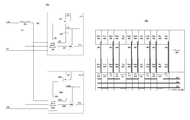
- FIG. 3 a is a block diagram of an example embodiment of a system 301 in accordance with the prior art. This system 301 is shown to illustrate some differences between a lumped boosting element system (e.g., the system 301 ) and a distributed boosting element system (e.g., system 300 of FIG. 3 b ).
- a lumped boosting element system e.g., the system 301
- a distributed boosting element system e.g., system 300 of FIG. 3 b
- the system 301 may include a memory array.
- the memory array may include a plurality of memory cells 302 arranged in words. In the illustrated embodiment, only a few bits of each word are shown. These words of memory cells 302 may be separated by merge logic 303 .
- the IO logic 304 may detect the appropriate word line for the request.
- the control logic 306 may then control the signals used to activate the proper word-line driver 312 , and word-line signal 349 . Via the activation of the appropriate word-line signal 349 , the desired or target word of the memory access may be accessed.
- a lumped boost capacitor 308 may be included in the system 301 .
- this lumped boost capacitor 308 may include a lumped switch, as described above.
- a clock signal 392 may travel through-out the drivers 312 and to the lumped boost capacitor 308 .
- the clock signal 392 may result in a word-line clock 322 and may also result in a boost net signal 324 .
- the word-line clock 322 is generated by the control logic 306 and the boost net signal 324 is generated by the lumped boost capacitor circuit 308 , they may not be aligned. As such the timing of the virtual voltage 342 may be negatively affected. Further, as the virtual voltage 342 is generated in a central location and travels throughout the drivers 312 , the voltage seen by the nearer versus farther away drivers 312 may differ. In various embodiments, this may not be desirable.
- FIG. 3 b is a block diagram of an example embodiment of a system 300 in accordance with the disclosed subject matter. In the illustrated embodiment, a distributed boosting element scheme is shown.
- the system 300 may include a memory array that includes a plurality of memory cells 302 arranged in words. In the illustrated embodiment, only a few bits of each word are shown. These words of memory cells 302 may be separated by merge logic 303 .
- the IO logic 304 may detect the appropriate word line for the request.
- the control logic 306 may then control the signals used to activate the proper word-line driver 312 , and word-line signal 349 . Via the activation of the appropriate word-line signal 349 , the desired or target word of the memory access may be accessed.
- each distributed boosting circuit 314 may include a distributed boosting element or capacitor and a distributed switch, transistor, or power-gater.
- each distributed boosting element may be co-located with a respective distributed switch.
- a distributed boosting circuit 314 may be thought of as a distributed voltage boosted circuit (similar to the voltage boosted circuit 101 of FIG. 1 ).
- the word-line clock signal 324 and the boosting net or boosting network control signal 322 may be generated by the control logic 306 .
- the word-line clock signal 324 and the boosting net signal 322 may be substantially aligned, as described above.
- the word-line clock signal 324 and the boosting net signal 322 may be received (in an aligned fashion) by each of the plurality of distributed boosting circuits 314 .
- the distributed boosting circuits 314 may then each generate their respective versions of the virtual voltage 342 , as described above.
- This respective virtual voltage 342 may then be employed by the respective driver 312 to generate the world-line signal 349 at either the first or array voltage, or the second voltage.
- the plurality of word line drivers 312 may be arranged in blocks of word line drivers.
- each block may include a sub-portion of the plurality of word line drivers 312 .
- the distributed boost network may be arranged in blocks of boost capacitors or boosting circuits 314 , wherein each block of boosting circuits 314 is associated with at least one respective block of word line drivers 312 and co-located with the respective block of word line drivers 312 .
- FIG. 4 is a schematic block diagram of an information processing system 400 , which may include semiconductor devices formed according to principles of the disclosed subject matter.
- an information processing system 400 may include one or more of devices constructed according to the principles of the disclosed subject matter. In another embodiment, the information processing system 400 may employ or execute one or more techniques according to the principles of the disclosed subject matter.
- the information processing system 400 may include a computing device, such as, for example, a laptop, desktop, workstation, server, blade server, personal digital assistant, smartphone, tablet, and other appropriate computers, etc. or a virtual machine or virtual computing device thereof. In various embodiments, the information processing system 400 may be used by a user (not shown).
- a computing device such as, for example, a laptop, desktop, workstation, server, blade server, personal digital assistant, smartphone, tablet, and other appropriate computers, etc. or a virtual machine or virtual computing device thereof.
- the information processing system 400 may be used by a user (not shown).
- the information processing system 400 may further include a central processing unit (CPU), logic, or processor 410 .
- the processor 410 may include one or more functional unit blocks (FUBs) or combinational logic blocks (CLBs) 415 .
- a combinational logic block may include various Boolean logic operations (e.g., NAND, NOR, NOT, XOR, etc.), stabilizing logic devices (e.g., flip-flops, latches, etc.), other logic devices, or a combination thereof. These combinational logic operations may be configured in simple or complex fashion to process input signals to achieve a desired result.
- the disclosed subject matter is not so limited and may include asynchronous operations, or a mixture thereof.
- the combinational logic operations may comprise a plurality of complementary metal oxide semiconductors (CMOS) transistors.
- CMOS complementary metal oxide semiconductors
- these CMOS transistors may be arranged into gates that perform the logical operations; although it is understood that other technologies may be used and are within the scope of the disclosed subject matter.
- the information processing system 400 may further include a volatile memory 420 (e.g., a Random Access Memory (RAM), etc.).
- the information processing system 400 according to the disclosed subject matter may further include a non-volatile memory 430 (e.g., a hard drive, an optical memory, a NAND or Flash memory, etc.).
- a volatile memory 420 e.g., a Random Access Memory (RAM), etc.
- the information processing system 400 according to the disclosed subject matter may further include a non-volatile memory 430 (e.g., a hard drive, an optical memory, a NAND or Flash memory, etc.).
- a storage medium e.g., either the volatile memory 420 , the non-volatile memory 430 , or a combination or portions thereof may be referred to as a “storage medium”.
- the volatile memory 420 and/or the non-volatile memory 430 may be configured to store data in a semi-permanent or substantially permanent form.
- the information processing system 400 may include one or more network interfaces 440 configured to allow the information processing system 400 to be part of and communicate via a communications network.
- a Wi-Fi protocol may include, but are not limited to, Institute of Electrical and Electronics Engineers (IEEE) 802.11g, IEEE 802.11n, etc.
- IEEE 802.11g Institute of Electrical and Electronics Engineers 802.11g
- IEEE 802.11n etc.
- a cellular protocol may include, but are not limited to: IEEE 802.16m (a.k.a. Wireless-MAN (Metropolitan Area Network) Advanced), Long Term Evolution (LTE) Advanced), Enhanced Data rates for GSM (Global System for Mobile Communications) Evolution (EDGE), Evolved High-Speed Packet Access (HSPA+), etc.
- Examples of a wired protocol may include, but are not limited to, IEEE 802.3 (a.k.a. Ethernet), Fibre Channel, Power Line communication (e.g., HomePlug, IEEE 1901, etc.), etc. It is understood that the above are merely a few illustrative examples to which the disclosed subject matter is not limited.
- the information processing system 400 may further include a user interface unit 450 (e.g., a display adapter, a haptic interface, a human interface device, etc.).
- this user interface unit 450 may be configured to either receive input from a user and/or provide output to a user.
- Other kinds of devices can be used to provide for interaction with a user as well; for example, feedback provided to the user can be any form of sensory feedback, e.g., visual feedback, auditory feedback, or tactile feedback; and input from the user can be received in any form, including acoustic, speech, or tactile input.
- the information processing system 400 may include one or more other devices or hardware components 460 (e.g., a display or monitor, a keyboard, a mouse, a camera, a fingerprint reader, a video processor, etc.). It is understood that the above are merely a few illustrative examples to which the disclosed subject matter is not limited.
- devices or hardware components 460 e.g., a display or monitor, a keyboard, a mouse, a camera, a fingerprint reader, a video processor, etc.
- the information processing system 400 may further include one or more system buses 405 .
- the system bus 405 may be configured to communicatively couple the processor 410 , the volatile memory 420 , the non-volatile memory 430 , the network interface 440 , the user interface unit 450 , and one or more hardware components 460 .
- Data processed by the processor 410 or data inputted from outside of the non-volatile memory 430 may be stored in either the non-volatile memory 430 or the volatile memory 420 .
- the information processing system 400 may include or execute one or more software components 470 .
- the software components 470 may include an operating system (OS) and/or an application.
- the OS may be configured to provide one or more services to an application and manage or act as an intermediary between the application and the various hardware components (e.g., the processor 410 , a network interface 440 , etc.) of the information processing system 400 .
- the information processing system 400 may include one or more native applications, which may be installed locally (e.g., within the non-volatile memory 430 , etc.) and configured to be executed directly by the processor 410 and directly interact with the OS.
- the native applications may include pre-compiled machine executable code.
- the native applications may include a script interpreter (e.g., C shell (csh), AppleScript, AutoHotkey, etc.) or a virtual execution machine (VM) (e.g., the Java Virtual Machine, the Microsoft Common Language Runtime, etc.) that are configured to translate source or object code into executable code which is then executed by the processor 410 .
- a script interpreter e.g., C shell (csh), AppleScript, AutoHotkey, etc.
- VM virtual execution machine
- semiconductor devices described above may be encapsulated using various packaging techniques.
- semiconductor devices constructed according to principles of the disclosed subject matter may be encapsulated using any one of a package on package (POP) technique, a ball grid arrays (BGAs) technique, a chip scale packages (CSPs) technique, a plastic leaded chip carrier (PLCC) technique, a plastic dual in-line package (PDIP) technique, a die in waffle pack technique, a die in wafer form technique, a chip on board (COB) technique, a ceramic dual in-line package (CERDIP) technique, a plastic metric quad flat package (PMQFP) technique, a plastic quad flat package (PQFP) technique, a small outline package (SOIC) technique, a shrink small outline package (SSOP) technique, a thin small outline package (TSOP) technique, a thin quad flat package (TQFP) technique, a system in package (SIP) technique, a multi-chip package (MCP) technique, a wafer-level fabricated package
- Method steps may be performed by one or more programmable processors executing a computer program to perform functions by operating on input data and generating output. Method steps also may be performed by, and an apparatus may be implemented as, special purpose logic circuitry, e.g., an FPGA (field programmable gate array) or an ASIC (application-specific integrated circuit).
- FPGA field programmable gate array
- ASIC application-specific integrated circuit
- a computer readable medium may include instructions that, when executed, cause a device to perform at least a portion of the method steps.
- the computer readable medium may be included in a magnetic medium, optical medium, other medium, or a combination thereof (e.g., CD-ROM, hard drive, a read-only memory, a flash drive, etc.).
- the computer readable medium may be a tangibly and non-transitorily embodied article of manufacture.
Landscapes
- Engineering & Computer Science (AREA)
- Power Engineering (AREA)
- Microelectronics & Electronic Packaging (AREA)
- Dc-Dc Converters (AREA)
- Semiconductor Integrated Circuits (AREA)
- Static Random-Access Memory (AREA)
- Dram (AREA)
- Semiconductor Memories (AREA)
Priority Applications (4)
| Application Number | Priority Date | Filing Date | Title |
|---|---|---|---|
| US14/813,103 US9502119B2 (en) | 2014-11-20 | 2015-07-29 | Distributed capacitive delay tracking boost-assist circuit |
| KR1020150159782A KR102427825B1 (ko) | 2014-11-20 | 2015-11-13 | 분배된 커패시티브 지연 추적 부스트-지원 회로 |
| JP2015226232A JP6560965B2 (ja) | 2014-11-20 | 2015-11-19 | 分配されたキャパシティブ遅延追跡ブーストの支援回路 |
| CN201510812067.XA CN105788621B (zh) | 2014-11-20 | 2015-11-20 | 升压设备、存储器系统和存储器设备 |
Applications Claiming Priority (2)
| Application Number | Priority Date | Filing Date | Title |
|---|---|---|---|
| US201462082611P | 2014-11-20 | 2014-11-20 | |
| US14/813,103 US9502119B2 (en) | 2014-11-20 | 2015-07-29 | Distributed capacitive delay tracking boost-assist circuit |
Publications (2)
| Publication Number | Publication Date |
|---|---|
| US20160148659A1 US20160148659A1 (en) | 2016-05-26 |
| US9502119B2 true US9502119B2 (en) | 2016-11-22 |
Family
ID=56010861
Family Applications (1)
| Application Number | Title | Priority Date | Filing Date |
|---|---|---|---|
| US14/813,103 Active US9502119B2 (en) | 2014-11-20 | 2015-07-29 | Distributed capacitive delay tracking boost-assist circuit |
Country Status (4)
| Country | Link |
|---|---|
| US (1) | US9502119B2 (enExample) |
| JP (1) | JP6560965B2 (enExample) |
| KR (1) | KR102427825B1 (enExample) |
| CN (1) | CN105788621B (enExample) |
Families Citing this family (3)
| Publication number | Priority date | Publication date | Assignee | Title |
|---|---|---|---|---|
| CN106898371B (zh) * | 2017-02-24 | 2020-08-28 | 中国科学院上海微系统与信息技术研究所 | 三维存储器读出电路及其字线与位线电压配置方法 |
| US11170830B2 (en) * | 2020-02-11 | 2021-11-09 | Taiwan Semiconductor Manufacturing Company Limited | Word line driver for low voltage operation |
| CN115731964A (zh) * | 2021-08-27 | 2023-03-03 | 长鑫存储技术有限公司 | 存储器和存储器的制造方法 |
Citations (4)
| Publication number | Priority date | Publication date | Assignee | Title |
|---|---|---|---|---|
| US4506350A (en) * | 1981-03-03 | 1985-03-19 | Tokyo Shibaura Denki Kabushiki Kaisha | Non-volatile semiconductor memory system |
| US20080068901A1 (en) * | 2006-09-18 | 2008-03-20 | Sebastian Ehrenreich | Wordline Booster Circuit and Method of Operating a Wordline Booster Circuit |
| US20120147654A1 (en) * | 2010-12-13 | 2012-06-14 | Texas Instruments Incorporated | Ferroelectric Random Access Memory with Single Plate Line Pulse During Read |
| US20130064006A1 (en) * | 2011-09-12 | 2013-03-14 | Qualcomm Incorporated | Apparatus for Selective Word-Line Boost on a Memory Cell |
Family Cites Families (5)
| Publication number | Priority date | Publication date | Assignee | Title |
|---|---|---|---|---|
| KR0137317B1 (ko) * | 1994-12-29 | 1998-04-29 | 김광호 | 반도체 메모리소자의 활성싸이클에서 사용되는 승압회로 |
| JPH10228773A (ja) * | 1997-02-14 | 1998-08-25 | Hitachi Ltd | ダイナミック型ram |
| JP3412800B2 (ja) * | 1997-05-27 | 2003-06-03 | 富士通株式会社 | 電圧発生回路を有した半導体装置 |
| JP2001067868A (ja) * | 1999-08-31 | 2001-03-16 | Mitsubishi Electric Corp | 半導体記憶装置 |
| US8493812B2 (en) * | 2010-10-28 | 2013-07-23 | International Business Machines Corporation | Boost circuit for generating an adjustable boost voltage |
-
2015
- 2015-07-29 US US14/813,103 patent/US9502119B2/en active Active
- 2015-11-13 KR KR1020150159782A patent/KR102427825B1/ko active Active
- 2015-11-19 JP JP2015226232A patent/JP6560965B2/ja active Active
- 2015-11-20 CN CN201510812067.XA patent/CN105788621B/zh active Active
Patent Citations (4)
| Publication number | Priority date | Publication date | Assignee | Title |
|---|---|---|---|---|
| US4506350A (en) * | 1981-03-03 | 1985-03-19 | Tokyo Shibaura Denki Kabushiki Kaisha | Non-volatile semiconductor memory system |
| US20080068901A1 (en) * | 2006-09-18 | 2008-03-20 | Sebastian Ehrenreich | Wordline Booster Circuit and Method of Operating a Wordline Booster Circuit |
| US20120147654A1 (en) * | 2010-12-13 | 2012-06-14 | Texas Instruments Incorporated | Ferroelectric Random Access Memory with Single Plate Line Pulse During Read |
| US20130064006A1 (en) * | 2011-09-12 | 2013-03-14 | Qualcomm Incorporated | Apparatus for Selective Word-Line Boost on a Memory Cell |
Also Published As
| Publication number | Publication date |
|---|---|
| JP2016100041A (ja) | 2016-05-30 |
| US20160148659A1 (en) | 2016-05-26 |
| JP6560965B2 (ja) | 2019-08-14 |
| KR102427825B1 (ko) | 2022-08-01 |
| CN105788621A (zh) | 2016-07-20 |
| KR20160060557A (ko) | 2016-05-30 |
| CN105788621B (zh) | 2019-08-20 |
Similar Documents
| Publication | Publication Date | Title |
|---|---|---|
| US9647453B2 (en) | Dual supply memory | |
| US9602092B2 (en) | Dynamic margin tuning for controlling custom circuits and memories | |
| CN106961264B (zh) | 具有内部控制信号的低功率集成时钟门控单元 | |
| US10446201B2 (en) | Distributed global-bitline keeper/precharge/header circuit for low voltage operation | |
| US9502119B2 (en) | Distributed capacitive delay tracking boost-assist circuit | |
| KR102821723B1 (ko) | 추가 회로 없이 스캐너블 플립-플롭의 전력 소모를 감소시키는 방법 | |
| TWI826658B (zh) | 時脈閘控系統 | |
| US9697889B1 (en) | Method and apparatus for read assist to achieve robust static random access memory (SRAM) | |
| US10003325B2 (en) | System and method for providing an area efficient and design rule check (DRC) friendly power sequencer for digital circuits | |
| TWI834856B (zh) | 時脈閘控鎖存設備以及時脈閘控鎖存系統 | |
| US20220113756A1 (en) | Controlled Transition Between Configuration Mode and User Mode to Reduce Current-Resistance Voltage Drop | |
| US20160217227A1 (en) | Adaptive low power and high performance logic design and physical design techniques |
Legal Events
| Date | Code | Title | Description |
|---|---|---|---|
| AS | Assignment |
Owner name: SAMSUNG ELECTRONICS CO., LTD., KOREA, REPUBLIC OF Free format text: ASSIGNMENT OF ASSIGNORS INTEREST;ASSIGNORS:BAJKOWSKI, MACIEJ;HUBER, JAN-MICHAEL;RAVI, VENKATESA;SIGNING DATES FROM 20150720 TO 20150722;REEL/FRAME:036213/0295 |
|
| STCF | Information on status: patent grant |
Free format text: PATENTED CASE |
|
| MAFP | Maintenance fee payment |
Free format text: PAYMENT OF MAINTENANCE FEE, 4TH YEAR, LARGE ENTITY (ORIGINAL EVENT CODE: M1551); ENTITY STATUS OF PATENT OWNER: LARGE ENTITY Year of fee payment: 4 |
|
| MAFP | Maintenance fee payment |
Free format text: PAYMENT OF MAINTENANCE FEE, 8TH YEAR, LARGE ENTITY (ORIGINAL EVENT CODE: M1552); ENTITY STATUS OF PATENT OWNER: LARGE ENTITY Year of fee payment: 8 |