US9460841B2 - Integrated inductor device with high inductance in a radiofrequency identification system - Google Patents
Integrated inductor device with high inductance in a radiofrequency identification system Download PDFInfo
- Publication number
- US9460841B2 US9460841B2 US13/437,843 US201213437843A US9460841B2 US 9460841 B2 US9460841 B2 US 9460841B2 US 201213437843 A US201213437843 A US 201213437843A US 9460841 B2 US9460841 B2 US 9460841B2
- Authority
- US
- United States
- Prior art keywords
- coil
- insulator layer
- module
- article
- disposed over
- Prior art date
- Legal status (The legal status is an assumption and is not a legal conclusion. Google has not performed a legal analysis and makes no representation as to the accuracy of the status listed.)
- Active, expires
Links
- 239000000853 adhesive Substances 0.000 claims abstract description 42
- 230000001070 adhesive effect Effects 0.000 claims abstract description 42
- 239000004020 conductor Substances 0.000 claims abstract description 10
- 239000000758 substrate Substances 0.000 claims description 86
- 229910000679 solder Inorganic materials 0.000 claims description 17
- 239000003292 glue Substances 0.000 claims description 11
- 230000002093 peripheral effect Effects 0.000 claims description 10
- 150000002894 organic compounds Chemical class 0.000 claims description 3
- QCEUXSAXTBNJGO-UHFFFAOYSA-N [Ag].[Sn] Chemical compound [Ag].[Sn] QCEUXSAXTBNJGO-UHFFFAOYSA-N 0.000 claims description 2
- PQIJHIWFHSVPMH-UHFFFAOYSA-N [Cu].[Ag].[Sn] Chemical compound [Cu].[Ag].[Sn] PQIJHIWFHSVPMH-UHFFFAOYSA-N 0.000 claims description 2
- 229910000969 tin-silver-copper Inorganic materials 0.000 claims description 2
- 239000012212 insulator Substances 0.000 claims 23
- 239000000463 material Substances 0.000 abstract description 12
- 238000000034 method Methods 0.000 abstract description 8
- 230000008569 process Effects 0.000 abstract description 5
- 230000008878 coupling Effects 0.000 abstract description 2
- 238000010168 coupling process Methods 0.000 abstract description 2
- 238000005859 coupling reaction Methods 0.000 abstract description 2
- 239000010410 layer Substances 0.000 description 50
- 239000002184 metal Substances 0.000 description 25
- 229910052751 metal Inorganic materials 0.000 description 25
- 238000004519 manufacturing process Methods 0.000 description 14
- 238000012216 screening Methods 0.000 description 10
- 238000004026 adhesive bonding Methods 0.000 description 5
- 238000005520 cutting process Methods 0.000 description 4
- 239000004033 plastic Substances 0.000 description 4
- 238000006116 polymerization reaction Methods 0.000 description 4
- RYGMFSIKBFXOCR-UHFFFAOYSA-N Copper Chemical compound [Cu] RYGMFSIKBFXOCR-UHFFFAOYSA-N 0.000 description 3
- 229910052802 copper Inorganic materials 0.000 description 3
- 239000010949 copper Substances 0.000 description 3
- 239000012792 core layer Substances 0.000 description 3
- 239000003302 ferromagnetic material Substances 0.000 description 3
- 239000011521 glass Substances 0.000 description 3
- 239000011810 insulating material Substances 0.000 description 3
- 238000001465 metallisation Methods 0.000 description 3
- 239000011111 cardboard Substances 0.000 description 2
- 239000003989 dielectric material Substances 0.000 description 2
- 239000003365 glass fiber Substances 0.000 description 2
- 238000010438 heat treatment Methods 0.000 description 2
- 230000015654 memory Effects 0.000 description 2
- 239000011859 microparticle Substances 0.000 description 2
- 239000002245 particle Substances 0.000 description 2
- 238000007747 plating Methods 0.000 description 2
- 125000006850 spacer group Chemical group 0.000 description 2
- 230000003068 static effect Effects 0.000 description 2
- JYEUMXHLPRZUAT-UHFFFAOYSA-N 1,2,3-triazine Chemical compound C1=CN=NN=C1 JYEUMXHLPRZUAT-UHFFFAOYSA-N 0.000 description 1
- XQUPVDVFXZDTLT-UHFFFAOYSA-N 1-[4-[[4-(2,5-dioxopyrrol-1-yl)phenyl]methyl]phenyl]pyrrole-2,5-dione Chemical compound O=C1C=CC(=O)N1C(C=C1)=CC=C1CC1=CC=C(N2C(C=CC2=O)=O)C=C1 XQUPVDVFXZDTLT-UHFFFAOYSA-N 0.000 description 1
- OKTJSMMVPCPJKN-UHFFFAOYSA-N Carbon Chemical compound [C] OKTJSMMVPCPJKN-UHFFFAOYSA-N 0.000 description 1
- 239000004593 Epoxy Substances 0.000 description 1
- BQCADISMDOOEFD-UHFFFAOYSA-N Silver Chemical compound [Ag] BQCADISMDOOEFD-UHFFFAOYSA-N 0.000 description 1
- 229910045601 alloy Inorganic materials 0.000 description 1
- 239000000956 alloy Substances 0.000 description 1
- 239000000560 biocompatible material Substances 0.000 description 1
- 230000015572 biosynthetic process Effects 0.000 description 1
- 229910052799 carbon Inorganic materials 0.000 description 1
- 239000000919 ceramic Substances 0.000 description 1
- 239000002131 composite material Substances 0.000 description 1
- 238000005260 corrosion Methods 0.000 description 1
- 230000007797 corrosion Effects 0.000 description 1
- 230000001808 coupling effect Effects 0.000 description 1
- 238000000151 deposition Methods 0.000 description 1
- 230000008021 deposition Effects 0.000 description 1
- 230000000694 effects Effects 0.000 description 1
- 238000005516 engineering process Methods 0.000 description 1
- 239000003822 epoxy resin Substances 0.000 description 1
- 230000005294 ferromagnetic effect Effects 0.000 description 1
- 239000000945 filler Substances 0.000 description 1
- 230000004907 flux Effects 0.000 description 1
- 230000006870 function Effects 0.000 description 1
- 230000009477 glass transition Effects 0.000 description 1
- MSNOMDLPLDYDME-UHFFFAOYSA-N gold nickel Chemical compound [Ni].[Au] MSNOMDLPLDYDME-UHFFFAOYSA-N 0.000 description 1
- 238000002347 injection Methods 0.000 description 1
- 239000007924 injection Substances 0.000 description 1
- 238000009413 insulation Methods 0.000 description 1
- 230000005291 magnetic effect Effects 0.000 description 1
- 239000012567 medical material Substances 0.000 description 1
- 238000004021 metal welding Methods 0.000 description 1
- 238000012986 modification Methods 0.000 description 1
- 230000004048 modification Effects 0.000 description 1
- 239000012811 non-conductive material Substances 0.000 description 1
- 230000003287 optical effect Effects 0.000 description 1
- 239000000123 paper Substances 0.000 description 1
- 239000011087 paperboard Substances 0.000 description 1
- 235000011837 pasties Nutrition 0.000 description 1
- 229920003192 poly(bis maleimide) Polymers 0.000 description 1
- 239000004417 polycarbonate Substances 0.000 description 1
- 229920000515 polycarbonate Polymers 0.000 description 1
- 229920000647 polyepoxide Polymers 0.000 description 1
- 239000005020 polyethylene terephthalate Substances 0.000 description 1
- 239000002861 polymer material Substances 0.000 description 1
- 238000007639 printing Methods 0.000 description 1
- 229910052709 silver Inorganic materials 0.000 description 1
- 239000004332 silver Substances 0.000 description 1
- 239000002356 single layer Substances 0.000 description 1
- 239000002904 solvent Substances 0.000 description 1
- 238000007669 thermal treatment Methods 0.000 description 1
Images


Classifications
-
- H—ELECTRICITY
- H01—ELECTRIC ELEMENTS
- H01F—MAGNETS; INDUCTANCES; TRANSFORMERS; SELECTION OF MATERIALS FOR THEIR MAGNETIC PROPERTIES
- H01F17/00—Fixed inductances of the signal type
- H01F17/0006—Printed inductances
- H01F17/0013—Printed inductances with stacked layers
Definitions
- An embodiment relates to an integrated inductor device with high inductance, for example for use as an antenna in a radiofrequency identification system.
- the medical field sees an increasingly widespread use of devices based on MEMS resonators that can withstand difficult conditions and operate as radio frequency identification (RFID) memories, in which the resonators are activated by the magnetic field generated by the current flowing in an antenna.
- RFID radio frequency identification
- the antenna should meet some requirements, such as having an inductance value on the order of microHenries ( ⁇ H), a small size, and a low cost. It has already been suggested to make the antenna on a BGA/LGA (Ball Grid Array/Land Grid Array) substrate. These substrates are formed by a plurality of overlaid conductive tracks (generally of copper, each formed in a conductive layer), and insulated from each other by insulating material layers. Holes, referred to as “vias”, allow electric contact through different insulating layers of the substrate.
- BGA/LGA All Grid Array/Land Grid Array
- the electric contact in the holes is obtained by the metallization of the inner surface of the holes, obtained by a process of electrochemical plating or by applying a conductive material layer and by screening and a subsequent high temperature baking.
- Another method to produce the electric contact through the holes consists in totally filling the latter with an adhesive charged with conductive particles by screening and baking, or by injection and baking and baking the conductive adhesive.
- the holes mutually couple the conductive tracks so as to form a plurality of conductive paths.
- the antenna for the memories or other RFID device may be produced on one of the main surfaces of the BGA/LGA substrate, for example as a miniaturized loop antenna, formed by a track of copper or other conducting material.
- An embodiment is an integrated inductor device that overcomes the drawbacks of the prior art.
- an inductor device is formed by superimposing a plurality of substrates or modules having the same structure.
- each coil is associated to at least one first adhesive conductive region that achieves the mechanical connection with an adjacent substrate (module) and to at least one second adhesive conductive region that achieves the electric connection with the coil formed in the adjacent substrate (module) and the first and second adhesive conductive regions are made of the same material and are arranged at a same level.
- each module is made as a BGA/LGA substrate, including at most four metallization levels.
- an overall inductance on the order of one ⁇ H can be obtained with a simple layout and a reduced area (for example, about 3.6 mm 2 ).
- Adhesive conductive regions formed by conductive glue or solder paste formed on the mutually facing surfaces of the overlaid modules allow mechanical and electric coupling among the various modules, in a simple and effective manner.
- each module is formed by a substrate carrying a coil made by applying conductive material.
- the same conductive layer forming the coil also forms electric contact regions and mechanical connection regions. After stacking a plurality of modules, the latter are glued by using the mechanical connection regions.
- the stacking can occur at a board level, each board integrating a plurality of identical modules and the single devices being obtained by cutting overlaid boards, or at a single-module level, by gluing to a first board single devices formed in a second board, which has been previously cut, and then also cutting the first board.
- FIG. 1 is a cross-section of an embodiment of the present integrated inductor
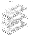
- FIG. 2 is an exploded perspective view of a part of the integrated inductor of FIG. 1 ;
- FIGS. 3 a -3 d show the layout of the four layers forming an upper module of the integrated inductor of FIG. 1 ;
- FIGS. 4 a -4 d show the layout of the four layers forming a first intermediate module of the integrated inductor of FIG. 1 ;
- FIGS. 5 a -5 d show the layout of the four layers of a second intermediate module of the integrated inductor of FIG. 1 ;
- FIGS. 6 a -6 d show the layout of the four layers of the bottom module of the integrated inductor of FIG. 1 ;
- FIG. 7 shows a board integrating a plurality of identical modules for the formation of a plurality of integrated inductors of the type shown in FIG. 1 ;
- FIGS. 8 and 9 are perspective views in two subsequent manufacturing steps of a first substrate, usable in a different embodiment of the present integrated inductor
- FIGS. 10 and 11 are perspective views in two subsequent manufacturing steps of a second substrate, usable with the substrate of FIGS. 8 and 9 ;
- FIG. 12 shows an integrated inductor which can be obtained by alternately superimposing a plurality of substrates according to FIGS. 9 and 11 ;
- FIG. 13 shows a board integrating a plurality of substrates of the type shown in FIG. 8 ;
- FIG. 14 shows subsequent manufacturing steps of integrated inductors, according to an embodiment.
- FIG. 15 shows the cross-section of a detail of a variant of the inductor of FIG. 12 .
- FIG. 1 shows a first embodiment of an integrated inductor 1 formed by a plurality of overlaid modules 2 - 5 having a similar structure, each incorporating four coils 25 which are overlaid so as to have the center aligned along a single central axis A and to be mutually coupled.
- the directly overlaid coils are wound in opposite directions so that the current always flows in a single direction (clockwise or counterclockwise).
- the plurality of modules 2 - 5 includes in this case six modules, including a first end module, typically an upper module 2 , a second end module, typically a bottom module 5 , two first intermediate modules 3 and two second intermediate modules 4 , the first and the second intermediate modules 3 , 4 being alternated.
- Modules 2 - 5 are manufactured according to the BGA technique, each having four metal layers, one for each coil, and differ only slightly in the layout.
- each of the modules 2 - 5 is formed by a first insulating layer 10 , a first metal layer 11 , a second insulating layer 12 , a second metal layer 13 , a core layer 15 , a third metal layer 17 , a third insulating layer 18 , a fourth metal layer 19 , and a fourth insulating layer 20 .
- the first and the fourth insulating layer 10 , 20 respectively forming the upper layer and the bottom layer of each module 2 - 5 are typically made as solder masks, i.e. of a non-conductive material that may be shaped by screening, for example of polymer material, such as, among others, AUS 308 material of Taiyo America, Inc.
- the second and the third insulating layers 12 and 18 are so-called “prepreg” layers i.e. each formed by, for example, a BT laminate containing crossed glass fibres therein, which ensure rigidity and a reduced temperature expansion.
- Core layer 15 is of an insulating material, typically plastic, for example a BT (Bismaleimide Triazine) or FR-4 or other material of printed circuits.
- plastic for example a BT (Bismaleimide Triazine) or FR-4 or other material of printed circuits.
- Metal layers 11 , 13 , 17 , 19 are, for example, of copper with an upper, corrosion protecting layer, typically of nickel-gold, and are shaped so as to each form a respective coil 25 as well as pads for the connections, including at least, for each metal layer, an input pad 26 and an output pad 27 (in which the indication “input” and “output” refer to the current direction shown, as explained above, and are not limitative). Furthermore, first and fourth metal layers 11 , 19 of all modules 2 - 4 also each form a connection pad 28 and the first metal layer 11 of upper module 2 forms an output terminal 29 ( FIG. 3 a ).
- the electric connections, together with the conductive vias passing through different modules 2 - 4 are configured and arranged so as to allow current to flow in coils 25 always in the same direction, as disclosed hereinafter.
- Coils 25 of metal layers 11 , 13 , 17 and 19 are each formed by a spiral, and the spirals of two overlaid layers are wound in opposite directions, but input pads 26 A- 26 P are arranged alternatively near the edge and near the center of the integrated inductor 1 . Therefore, coil 25 of first metal layer 11 of all modules 2 - 5 is wound in a counterclockwise direction from the outside and from its own input pad (input pad 26 A, 26 E, 26 I and 26 M, FIGS. 3 a , 4 a , 5 a and 6 a ), coil 25 of second metal layer 13 is wound from the outside in a clockwise direction (corresponding to a counterclockwise direction from its own input pad 26 B, 26 F, 26 J and 26 N, FIGS.
- coil 25 of third metal layer 17 is wound in a counterclockwise direction from the outside and from its own input pad (input pad 26 C, 26 G, 26 K and 26 O, FIGS. 3 c , 4 c , 5 c and 6 c ), and coil 25 of fourth metal layer 19 is wound from the outside in a clockwise direction (corresponding to a counterclockwise direction from its own input pad 26 D, 26 H, 26 L and 26 P, FIGS. 3 d , 4 d , 5 d and 6 d ).
- Output pads 27 A- 27 P of modules 2 - 4 are arranged vertically aligned to input pads 26 B- 26 P of the metal level immediately below, as may be noted easily from FIGS. 3 a -5 d . Accordingly, output pads 27 A- 27 P are also arranged alternatively near the edge or near the center of integrated inductor 1 .
- connection pads 28 of all the metal layers 2 - 5 are overlaid. Furthermore, connection pad 28 of fourth metal layer 19 of bottom module 5 also forms an output pad of the bottom module 5 .
- Conductive vias 30 - 33 completely pass through each module 2 - 4 , but vias 30 - 32 each couple reciprocally, in each module, a single output pad with the immediately underlying input pad, whereas vias 33 couple all the connection pads 28 to each other.
- vias 30 , 31 are arranged near the center of integrated inductor 1 ; vias 32 - 33 are arranged near the edge.
- conductive via 30 passes through and electrically couples output pad 27 A to input pad 26 B (both in a central position); conductive via 31 passes through and electrically couples output pad 27 C to input pad 26 D.
- FIGS. 3 b , 3 c via 32 (not visible in FIG.
- vias 30 - 32 of modules 5 - 4 respectively couple the output pads to the directly underlying input pads, as may be seen in FIGS. 4 a - 6 d.
- Output pads 27 D, 27 H and 27 L of fourth metal level 19 of modules 2 - 4 are instead coupled to input pads 26 E, 26 I and 26 M of an underlying level (first metal level 13 of modules 3 - 5 ) by first electric connection regions 35 , represented by a shaded line in FIGS. 3 a - 6 d.
- vias 33 of modules 2 - 5 are reciprocally coupled to each other by second electric connection regions 36 ; mechanical connection regions 37 mechanically couple modules 2 - 5 to each other.
- Mechanical connection regions 37 extend peripherally near the edges of relative modules 2 - 5 on both sides thereof, except for the sides intended to form the upper surface and the lower surface of integrated inductor 1 .
- First and second electric connection regions 35 , 36 and mechanical connection regions 37 form adhesive conductive regions extending, for each upper and lower surface of modules 2 - 5 , horizontally aligned (on a same level) in corresponding openings 39 of the first and fourth insulating layers 10 , 20 of modules 2 - 5 , except for, as indicated, mechanical connection regions 37 of the upper and lower surfaces of inductor 1 and are formed by the same material, applied approximately simultaneously, for example, a conductive glue (containing, for example, an Ag filler) or a tin-silver, tin-silver-copper, or other lead-free metal welding alloy.
- a conductive glue containing, for example, an Ag filler
- tin-silver-copper or other lead-free metal welding alloy.
- Integrated inductor 1 is manufactured as follows according to an embodiment.
- FIG. 7 shows a part thereof.
- Each board is formed by a plurality of approximately identical modules 2 , 3 , 4 , or 5 .
- FIG. 7 shows a plurality of upper modules 2 .
- Boards 40 are manufactured according to known technologies, so that each module 2 - 5 has the disclosed configuration. Therefore, a conductive adhesive or a lead-free paste is applied by screening or dispensing on the side areas of first and fourth insulating layers 10 , 20 and over output pads 27 and vias 33 to form regions 35 - 37 ; therefore, boards 40 relative to the various modules are overlaid and reciprocally glued.
- the adhesive conductive vias 35 - 37 are made by conductive glues
- boards 40 are subjected to a thermal treatment at a polymerization-initiation temperature lower than the glass-transition temperature of the glue (depending on the type of glue), in order to obtain a sufficient adhesion of adhesive conductive regions 35 - 37 and to maintain the overlaid modules in position.
- the polymerization of the adhesive is completed in a static oven or a tunnel depending on the features of the adhesive.
- adhesive conductive regions 35 - 37 are made by a solder paste
- a reflow process is performed in standard conditions for lead-free solder pastes with a peak temperature of 260° C.
- the alignment in the plane of the boards is performed by optical positioning machines, which take the first board as a reference using references (designated “fiducials”) made on the first board for metal plating, screening, marking, cutting, or boring.
- references designated “fiducials”
- the superimposition may be performed by a support with metal plugs that pass through centering holes made on the boards. The supports are then used for baking in static or tunnel ovens of the stacked boards and then removed before cutting.
- core layer 15 can have a thickness in the range approximately between 60 and 110 ⁇ m, for example approximately 100 ⁇ m
- first and fourth insulating layers 10 , 20 , of solder mask can have a thickness of about 20 ⁇ m
- second and third insulating layers 12 and 18 , of prepreg can have an overall thickness in the range approximately between 30 and 40 ⁇ m
- metal layers 11 , 13 , 17 and 19 can have a thickness of about 17 ⁇ m for an overall thickness of each module 2 - 5 generally variable approximately between 220 (in case of thin device) and 300 ⁇ m (in case of standard device).
- FIGS. 8-13, 15 relate to a different embodiment of the present integrated inductor, wherein each module includes a single substrate (drilled to make the connections), on which a conductive track that forms a coil is made (for example by screening, dispensing, or printing).
- the processing occurs typically at a board level, each board forming a plurality of substrates that, after being superimposed and glued, are cut in a final step, to obtain the single inductors.
- the manufacturing steps are disclosed at a single substrate level.
- FIG. 8 shows a first substrate 50 provided with a first and a second surface 50 A, 50 B.
- the first substrate 50 may be one of a plurality of modules forming a board 75 , as shown in FIG. 13 .
- the first substrate 50 can be of any insulating material such as BT (Bismaleidetriazine) or epoxy resin charged with glass fibers, injected plastic, PET, polycarbonate, or other types of plastic material, ceramics, glass, paper, cardboard, and the like.
- the first substrate 50 can be of a ferromagnetic material with the two opposite faces coated with a dielectric material layer as disclosed more in detail hereinafter.
- biocompatible or medical materials can be selected.
- first substrate 50 is drilled to form two through holes 51 and 52 extending between surfaces 50 A, 50 B.
- first through hole 51 is central and second through hole 52 is arranged near the edge of first substrate 50 .
- through holes 51 and 52 are metallized.
- the holes are at first coated with a dielectric layer, typically an epoxy or glass paste, for example by screening and then baking, and then filled with an adhesive conductive material or with a solder paste.
- a conductive material is printed or dispensed on first surface 50 A of first substrate 50 so as to approximately simultaneously form a coil 55 and adhesive conductive regions forming both electric and mechanical connections.
- a conductive glue or a solder paste is applied, for example by screening, on the upper surface of first substrate 50 .
- the conductive material fills holes 51 and 52 (where it forms a first and a second via 53 and 54 ), forms a spiral (forming coil 55 ), a first contact region 56 and a peripheral region 59 .
- Coil 55 extends between first via 53 (and therefore first through hole 51 ) and first contact region 56 .
- First contact region 56 is made near the edge of first substrate 50 , near but distinct from the second via 54 and the peripheral region 59 surrounds, for example completely, the first substrate 50 .
- Peripheral region 59 is similar to mechanical connection regions 37 of the embodiments of FIGS. 1-7 and has the aim of allowing the mechanical connection between first substrate 50 and a second overlaid substrate, as explained hereinafter.
- the conductive material may be an adhesive material charged with conductive particles, or a lead-free solder paste formed by microparticles amalgamated with fluxes so as to obtain a pasty consistency, or a conductive ink.
- the adhesive materials are subjected to partial capture to control the extension thereof, thus avoiding short-circuiting between the coils and maintaining the adhesiveness thereof.
- spacers can be used.
- the spacers may be formed on the substrate, by previously dispensing adhesive cylinders of the same kind used for the manufacture of the inductance, or of a different kind, and by baking (for about an hour at a temperature of about 150° C.) so as to ensure a rigid support.
- a second substrate 60 (shown in FIG. 10 ) is manufactured independently. Second substrate 60 is similar to first substrate 50 , except for the position of the through-holes. Accordingly, the material of second substrate 60 may be any, possibly even another material with respect to first substrate 50 , and second substrate 60 has first and second surfaces 60 A, 60 B.
- second substrate 60 is drilled so as to form a third through hole 61 and a fourth through hole 62 .
- both through holes 61 , 62 are formed near the edge of second substrate 60 , with third through hole 61 in a position such as to be aligned, after the superimposition of substrates 50 , 60 , to first conductive region 56 of first substrate 50 , and fourth through hole 62 aligned (after the superimposition of the substrates) to the second through hole 52 .
- through holes 61 , 62 can be metallized.
- second substrate 60 can be part of a respective board (not shown), similar to board 75 of FIG. 13 .
- second substrate 60 is printed to form a respective coil 65 , a second contact region 66 , and an own peripheral region 59 .
- This step is carried out as already disclosed for first substrate 50 by applying a conductive glue or a solder paste, and also leads to the filling of fourth and fifth hole 61 , 62 .
- a third and fourth via 63 and 64 form in through holes 61 , 62 , and coil 65 extends between third via 63 and second contact region 66 .
- coil 65 of second substrate 60 is wound in an opposite direction with respect to coil 55 of first substrate 50 .
- coil 55 of first substrate 50 extends counterclockwise from the outside (first connection region 56 ) inwards (first via 53 ), while coil 65 of second substrate 60 extends clockwise from the outside (third through via 63 ) inwards (third connection region 66 ), so that the current always flows in the same direction, as explained hereinafter.
- second substrate 60 is superimposed over first substrate 50 , with surface 60 B in contact with surface 50 A, so that third via 63 is overlaid and electrically contacts first contact region 56 and fourth via 64 is overlaid and electrically contacts second via 54 .
- another first substrate 50 is superimposed over second substrate 60 so that first via 53 is overlaid vertically to third connection region 66 and second via 54 is overlaid vertically to fourth via 64 .
- the process of superimposition may be performed using fiducials (not shown), always referring each substrate 50 , 60 added on top, to the bottom substrate.
- the process continues with the alternated superimposition of first and second substrates 50 , 60 , to obtain an integrated inductor 70 , shown in FIG. 12 and formed by a stack of substrates 50 , 60 , for example 10 .
- the bottom substrate of the stack having the configuration of second substrate 60 of FIG. 11 , may not be preventively drilled and have, instead of third and fourth vias 63 , 64 , corresponding contact regions 67 , 68 ( FIG. 12 ) coupled to one another.
- the top substrate in the stack has the configuration of first substrate 50 of FIG. 9 , and may not have peripheral region 59 .
- first connection region 56 and the top portion of third via 54 can be shaped so as to form connection pads for the outer connection.
- substrates 50 and 60 can be subjected to a heating step in an oven, so as to increase the consistency of the adhesive conductive regions, in particular of peripheral regions 59 .
- the heating is performed at a temperature lower than the polymerization temperature, for example lower than about 100° C. for a time of about 10 minutes.
- substrates 50 and 60 are reciprocally glued, arranging the stack of substrates 50 , 60 in an oven at a temperature in the range approximately between 120-170° C., typically about 150° C., for about 1-2 hours, so as to obtain the polymerization of the conductive glue or solder paste and, therefore, the gluing of peripheral regions 59 of each substrate 50 , 60 to the overlaying substrate 60 , 50 , as well as of first and second contact regions 56 , 66 to the respective overlaying and underlying metallized vias 63 , 53 .
- substrates 50 , 60 are each part of a respective board including a plurality of substrates 50 or 60 , after gluing the stack is singulated to form single inductors 70 .
- first contact region 56 represents a current input and the end of second via 54 represents a current output
- the current always flows in a counterclockwise direction, entering the first contact region 56 of upper substrate 50 and flowing through first coil 55 up to first via 53 , which is in electrical contact with the second contact region 66 of second coil 65 ( FIG. 11 ) of underlying substrate 60 . Therefore the current also flows through second coil 65 in a counterclockwise direction up to third contact via 63 and from here reaches first contact region 56 of a first underlying substrate 50 .
- the current After flowing through all the coils in a counterclockwise direction, the current reaches contact regions 66 , 67 and then passes through second and fourth vias 54 , 64 , which are overlaid to one another, up to second via 54 of the overlaid substrate, which represents an output terminal of integrated inductor 70 .
- FIG. 15 shows a detail of a variant of the integrated inductor of FIG. 12 , using substrates 150 , 160 of a ferromagnetic material, covered by insulating layers 170 on the two faces.
- a coil 165 is formed on one of the faces (for example the top one) of substrates 150 , 160 .
- vias 161 (corresponding to vias 53 - 54 , 63 - 64 ) are insulated from corresponding substrate 150 , 160 by an insulation 162 .
- Insulating layers 170 can be screened and peripheral regions 159 (made approximately simultaneously to coils 165 and to contact regions which are not shown and are similar to contact regions 56 , 66 ) allow mutual gluing of substrates 150 , 160 . In this case, a further increase of the overall value of the inductance, as well as an increase in the mechanical resistance of the module, may be obtained.
- FIG. 14 shows a different manufacturing process.
- a first board 80 and a second board 81 each integrating coils in an opposite direction are manufactured independently.
- Boards 80 , 81 may be subjected to the same manufacturing steps disclosed above to obtain modules 2 - 5 of FIGS. 1-7 , for example modules 2 and 5 , or substrates 50 , 60 of FIGS. 9 and 11 . Therefore, according to the known technique of “pick and place”, first panel 80 is cut, so as to form a plurality of single elements 83 which are singularly taken and arranged over corresponding elements of second board 81 , on which (by dispensing or screening) a conductive adhesive or a solder paste has been preventively applied and which has been prebaked (in the case of conductive adhesive). After all single elements 83 have been arranged, these are glued to board 81 , for example by polymerization of peripheral region 59 .
- An embodiment of the integrated inductor and an embodiment of the corresponding manufacturing process, as disclosed herein, have several advantages.
- an embodiment of the present integrated inductor can be made of the desired value, even having a magnitude on the order of one pH, with a simple layout of the single layers and with limited manufacturing costs.
- the layers of the dielectric can be made thin, therefore helping the coupling effect among the various overlaid coils.
- the manufacture of the substrates of ferromagnetic material insulated by dielectrics allows to further increase the value of the overall inductance of the module.
- the adhesive conductive regions among different overlaid modules may be formed in the same manufacturing step and therefore may be of the same material and may be arranged on the same level (horizontal alignment). This provides a high mechanical and electrical resistance of the connections, as well as a simple manufacturing that requires limited costs.
- FIGS. 8-13 An embodiment of FIGS. 8-13 is advantageously usable in case the substrate is made of a non-conventional material, such as glass or plastic, if there are particular requirements, such as light mechanical flexibility.
- substrates 50 , 60 of the embodiment of FIGS. 8-13 can be made of paper or cardboard.
- the coils and the adhesive regions can be made of conductive ink, such as for example an ink made by charging an appropriate solvent with carbon or silver microparticles to an extent as to obtain a viscosity suitable for deposition by dispensing or screening.
- the through holes 51 , 52 and 61 , 62 may also be preventively metallized when vias 53 , 54 , 63 , 64 , 161 are made.
- the application of the conductive adhesive or of the solder paste in the through holes for forming the electrical connections through the substrates can take place approximately simultaneously to or before the manufacture of the inductance, and as a function of the ratio between the diameter of the hole and the thickness of the substrate (“aspect ratio”).
- the metal layers 11 , 13 , 17 , 19 of the embodiment of FIGS. 1-7 can be replaced by conductive layers, for example layers of an organic compound.
- contact regions 35 , 36 ; 56 , 66 can be formed by portions of respective coils 55 , 65 , 165 , without being distinct therefrom.
Landscapes
- Engineering & Computer Science (AREA)
- Power Engineering (AREA)
- Microelectronics & Electronic Packaging (AREA)
- Coils Or Transformers For Communication (AREA)
- Input Circuits Of Receivers And Coupling Of Receivers And Audio Equipment (AREA)
- Semiconductor Integrated Circuits (AREA)
Applications Claiming Priority (3)
| Application Number | Priority Date | Filing Date | Title |
|---|---|---|---|
| ITTO2011A0295 | 2011-04-01 | ||
| IT000295A ITTO20110295A1 (it) | 2011-04-01 | 2011-04-01 | Dispositivo ad induttore integrato ad elevato valore di induttanza, in particolare per l'uso come antenna in un sistema di identificazione a radiofrequenza |
| ITTO2011A000295 | 2011-04-01 |
Publications (2)
| Publication Number | Publication Date |
|---|---|
| US20120249276A1 US20120249276A1 (en) | 2012-10-04 |
| US9460841B2 true US9460841B2 (en) | 2016-10-04 |
Family
ID=44553997
Family Applications (1)
| Application Number | Title | Priority Date | Filing Date |
|---|---|---|---|
| US13/437,843 Active 2032-04-16 US9460841B2 (en) | 2011-04-01 | 2012-04-02 | Integrated inductor device with high inductance in a radiofrequency identification system |
Country Status (2)
| Country | Link |
|---|---|
| US (1) | US9460841B2 (it) |
| IT (1) | ITTO20110295A1 (it) |
Cited By (2)
| Publication number | Priority date | Publication date | Assignee | Title |
|---|---|---|---|---|
| US9899136B2 (en) * | 2016-05-13 | 2018-02-20 | Samsung Electro-Mechanics Co., Ltd. | Coil component and method of manufacturing the same |
| US10978240B2 (en) | 2017-05-01 | 2021-04-13 | Qualcomm Incorporated | Inductor with embraced corner capture pad |
Families Citing this family (10)
| Publication number | Priority date | Publication date | Assignee | Title |
|---|---|---|---|---|
| TWI604480B (zh) | 2012-03-23 | 2017-11-01 | Lg伊諾特股份有限公司 | 無線功率接收器以及包含有其之可攜式終端裝置 |
| JP6313744B2 (ja) | 2012-03-23 | 2018-04-18 | エルジー イノテック カンパニー リミテッド | 無線電力受信機 |
| TWM503638U (zh) * | 2014-12-22 | 2015-06-21 | Wistron Corp | 電感元件 |
| US9864985B2 (en) | 2015-01-14 | 2018-01-09 | Samsung Pay, Inc. | Transmitter and method for substantially reducing dead zones in an inductive contactless mobile payment system |
| CN106531410B (zh) | 2015-09-15 | 2019-08-27 | 臻绚电子科技(上海)有限公司 | 线圈,电感元件及制备应用于电感元件的线圈的方法 |
| US10692643B2 (en) | 2015-10-27 | 2020-06-23 | Cochlear Limited | Inductance coil path |
| US10692642B2 (en) | 2015-10-27 | 2020-06-23 | Cochlear Limited | Inductance coil with varied geometry |
| CN107453048B (zh) * | 2016-05-31 | 2021-03-12 | Skc株式会社 | 天线设备和包括天线设备的便携式终端 |
| US10770225B2 (en) * | 2016-08-08 | 2020-09-08 | Hamilton Sundstrand Corporation | Multilayered coils |
| JP6946721B2 (ja) | 2017-05-03 | 2021-10-06 | Tdk株式会社 | コイル部品 |
Citations (35)
| Publication number | Priority date | Publication date | Assignee | Title |
|---|---|---|---|---|
| US2911605A (en) * | 1956-10-02 | 1959-11-03 | Monroe Calculating Machine | Printed circuitry |
| EP0035964A1 (de) | 1980-03-07 | 1981-09-16 | Walch, Rudolf | Induktionsscheibenwicklung |
| US4959630A (en) | 1989-08-07 | 1990-09-25 | General Electric Company | High-frequency transformer |
| US5047719A (en) | 1990-05-25 | 1991-09-10 | The Failure Group, Inc. | Flexible coil assembly for reflectance-mode nondestructive eddy-current examination |
| JPH04206906A (ja) | 1990-11-30 | 1992-07-28 | Tokin Corp | 薄型トランス |
| JPH06251945A (ja) | 1993-02-24 | 1994-09-09 | Takeshi Ikeda | 積層型素子 |
| US5381124A (en) | 1993-12-29 | 1995-01-10 | General Electric Company | Multi-turn z-foldable secondary winding for a low-profile, conductive film transformer |
| US5532667A (en) * | 1992-07-31 | 1996-07-02 | Hughes Aircraft Company | Low-temperature-cofired-ceramic (LTCC) tape structures including cofired ferromagnetic elements, drop-in components and multi-layer transformer |
| WO1999003117A1 (de) | 1997-07-10 | 1999-01-21 | Melcher Ag | Multilayer-planarinduktivität und verfahren zum herstellen einer solchen |
| JPH1116729A (ja) | 1997-06-20 | 1999-01-22 | Japan Aviation Electron Ind Ltd | プリント配線型インダクタンス素子 |
| US6023114A (en) * | 1997-09-08 | 2000-02-08 | Ntn Corporation | Spindle motor and rotating shaft supporting device for spindle motor |
| EP1304707A2 (en) | 2001-10-19 | 2003-04-23 | Broadcom Corporation | Multiple layer inductor and method of making the same |
| US6628531B2 (en) * | 2000-12-11 | 2003-09-30 | Pulse Engineering, Inc. | Multi-layer and user-configurable micro-printed circuit board |
| US6716672B2 (en) * | 2000-02-11 | 2004-04-06 | 3D Plus | Three dimensional interconnection method and electronic device obtained by same |
| US20040075525A1 (en) | 2000-11-04 | 2004-04-22 | Sippola Mika Matti | Inductive components |
| JP2005222997A (ja) | 2004-02-03 | 2005-08-18 | Iq Four:Kk | コイルシート |
| US20060115931A1 (en) * | 2004-11-26 | 2006-06-01 | Phoenix Precision Technology Corporation | Semiconductor package substrate with embedded chip and fabrication method thereof |
| US20060158301A1 (en) * | 2004-05-28 | 2006-07-20 | Atsushi Shinkai | Common mode noise filter |
| US20070030659A1 (en) * | 2003-09-29 | 2007-02-08 | Yukiharu Suzuki | Multilayer laminated circuit board |
| US20070057755A1 (en) * | 2003-09-29 | 2007-03-15 | Yukiharu Suzuki | Solid electrolytic capacitor and manufacturing method thereof |
| US7369028B2 (en) * | 2004-11-25 | 2008-05-06 | Murata Manufacturing Co., Ltd. | Coil component |
| US20080238600A1 (en) | 2007-03-29 | 2008-10-02 | Olson Bruce D | Method of producing a multi-turn coil from folded flexible circuitry |
| US20080257488A1 (en) * | 2006-01-16 | 2008-10-23 | Murata Manufacturing Co., Ltd. | Method of manufacturing inductor |
| DE102007019111A1 (de) | 2007-04-23 | 2008-10-30 | Osram Gesellschaft mit beschränkter Haftung | Elektronisches Bauelement |
| US20080290528A1 (en) * | 2007-05-21 | 2008-11-27 | Phoenix Precision Technology Corporation | Semiconductor package substrate having electrical connecting pads |
| EP2109120A1 (en) | 2007-01-26 | 2009-10-14 | Panasonic Electric Works Co., Ltd | Laminated element |
| US7663225B2 (en) * | 2004-07-23 | 2010-02-16 | Murata Manufacturing Co., Ltd. | Method for manufacturing electronic components, mother substrate, and electronic component |
| US20100109123A1 (en) * | 2008-10-31 | 2010-05-06 | Bernhard Strzalkowski | Method of Constructing Inductors and Transformers |
| US20100157565A1 (en) * | 2008-12-22 | 2010-06-24 | Tdk Corporation | Electronic component and manufacturing method of electronic component |
| US20100289610A1 (en) * | 2009-05-12 | 2010-11-18 | Jacobson Boris S | Planar magnetic structure |
| US7859382B2 (en) * | 2008-09-26 | 2010-12-28 | Lincoln Global, Inc. | Planar transformer |
| US20110074535A1 (en) * | 2009-09-29 | 2011-03-31 | Murata Manufacturing Co., Ltd. | Multilayer coil device |
| US20110227688A1 (en) * | 2010-03-22 | 2011-09-22 | Samsung Electro-Mechanics Co., Ltd. | Planar transformer |
| US8390417B2 (en) * | 2008-09-22 | 2013-03-05 | Panasonic Corporation | Laminated electronic component |
| US8441333B2 (en) * | 2009-12-08 | 2013-05-14 | Shanghai Hua Hong Nec Electronics Company, Limited | Stack inductor with different metal thickness and metal width |
-
2011
- 2011-04-01 IT IT000295A patent/ITTO20110295A1/it unknown
-
2012
- 2012-04-02 US US13/437,843 patent/US9460841B2/en active Active
Patent Citations (35)
| Publication number | Priority date | Publication date | Assignee | Title |
|---|---|---|---|---|
| US2911605A (en) * | 1956-10-02 | 1959-11-03 | Monroe Calculating Machine | Printed circuitry |
| EP0035964A1 (de) | 1980-03-07 | 1981-09-16 | Walch, Rudolf | Induktionsscheibenwicklung |
| US4959630A (en) | 1989-08-07 | 1990-09-25 | General Electric Company | High-frequency transformer |
| US5047719A (en) | 1990-05-25 | 1991-09-10 | The Failure Group, Inc. | Flexible coil assembly for reflectance-mode nondestructive eddy-current examination |
| JPH04206906A (ja) | 1990-11-30 | 1992-07-28 | Tokin Corp | 薄型トランス |
| US5532667A (en) * | 1992-07-31 | 1996-07-02 | Hughes Aircraft Company | Low-temperature-cofired-ceramic (LTCC) tape structures including cofired ferromagnetic elements, drop-in components and multi-layer transformer |
| JPH06251945A (ja) | 1993-02-24 | 1994-09-09 | Takeshi Ikeda | 積層型素子 |
| US5381124A (en) | 1993-12-29 | 1995-01-10 | General Electric Company | Multi-turn z-foldable secondary winding for a low-profile, conductive film transformer |
| JPH1116729A (ja) | 1997-06-20 | 1999-01-22 | Japan Aviation Electron Ind Ltd | プリント配線型インダクタンス素子 |
| WO1999003117A1 (de) | 1997-07-10 | 1999-01-21 | Melcher Ag | Multilayer-planarinduktivität und verfahren zum herstellen einer solchen |
| US6023114A (en) * | 1997-09-08 | 2000-02-08 | Ntn Corporation | Spindle motor and rotating shaft supporting device for spindle motor |
| US6716672B2 (en) * | 2000-02-11 | 2004-04-06 | 3D Plus | Three dimensional interconnection method and electronic device obtained by same |
| US20040075525A1 (en) | 2000-11-04 | 2004-04-22 | Sippola Mika Matti | Inductive components |
| US6628531B2 (en) * | 2000-12-11 | 2003-09-30 | Pulse Engineering, Inc. | Multi-layer and user-configurable micro-printed circuit board |
| EP1304707A2 (en) | 2001-10-19 | 2003-04-23 | Broadcom Corporation | Multiple layer inductor and method of making the same |
| US20070030659A1 (en) * | 2003-09-29 | 2007-02-08 | Yukiharu Suzuki | Multilayer laminated circuit board |
| US20070057755A1 (en) * | 2003-09-29 | 2007-03-15 | Yukiharu Suzuki | Solid electrolytic capacitor and manufacturing method thereof |
| JP2005222997A (ja) | 2004-02-03 | 2005-08-18 | Iq Four:Kk | コイルシート |
| US20060158301A1 (en) * | 2004-05-28 | 2006-07-20 | Atsushi Shinkai | Common mode noise filter |
| US7663225B2 (en) * | 2004-07-23 | 2010-02-16 | Murata Manufacturing Co., Ltd. | Method for manufacturing electronic components, mother substrate, and electronic component |
| US7369028B2 (en) * | 2004-11-25 | 2008-05-06 | Murata Manufacturing Co., Ltd. | Coil component |
| US20060115931A1 (en) * | 2004-11-26 | 2006-06-01 | Phoenix Precision Technology Corporation | Semiconductor package substrate with embedded chip and fabrication method thereof |
| US20080257488A1 (en) * | 2006-01-16 | 2008-10-23 | Murata Manufacturing Co., Ltd. | Method of manufacturing inductor |
| EP2109120A1 (en) | 2007-01-26 | 2009-10-14 | Panasonic Electric Works Co., Ltd | Laminated element |
| US20080238600A1 (en) | 2007-03-29 | 2008-10-02 | Olson Bruce D | Method of producing a multi-turn coil from folded flexible circuitry |
| DE102007019111A1 (de) | 2007-04-23 | 2008-10-30 | Osram Gesellschaft mit beschränkter Haftung | Elektronisches Bauelement |
| US20080290528A1 (en) * | 2007-05-21 | 2008-11-27 | Phoenix Precision Technology Corporation | Semiconductor package substrate having electrical connecting pads |
| US8390417B2 (en) * | 2008-09-22 | 2013-03-05 | Panasonic Corporation | Laminated electronic component |
| US7859382B2 (en) * | 2008-09-26 | 2010-12-28 | Lincoln Global, Inc. | Planar transformer |
| US20100109123A1 (en) * | 2008-10-31 | 2010-05-06 | Bernhard Strzalkowski | Method of Constructing Inductors and Transformers |
| US20100157565A1 (en) * | 2008-12-22 | 2010-06-24 | Tdk Corporation | Electronic component and manufacturing method of electronic component |
| US20100289610A1 (en) * | 2009-05-12 | 2010-11-18 | Jacobson Boris S | Planar magnetic structure |
| US20110074535A1 (en) * | 2009-09-29 | 2011-03-31 | Murata Manufacturing Co., Ltd. | Multilayer coil device |
| US8441333B2 (en) * | 2009-12-08 | 2013-05-14 | Shanghai Hua Hong Nec Electronics Company, Limited | Stack inductor with different metal thickness and metal width |
| US20110227688A1 (en) * | 2010-03-22 | 2011-09-22 | Samsung Electro-Mechanics Co., Ltd. | Planar transformer |
Non-Patent Citations (2)
| Title |
|---|
| Search Report for Italian Application No. TO20110295, Ministero dello Sviluppo Economico, Munich, Nov. 22, 2011, pp. 2. |
| Search Report for Italian Application No. TO20110296, Ministero dello Sviluppo Economico, Munich, Jan. 24, 2012, pp. 3. |
Cited By (2)
| Publication number | Priority date | Publication date | Assignee | Title |
|---|---|---|---|---|
| US9899136B2 (en) * | 2016-05-13 | 2018-02-20 | Samsung Electro-Mechanics Co., Ltd. | Coil component and method of manufacturing the same |
| US10978240B2 (en) | 2017-05-01 | 2021-04-13 | Qualcomm Incorporated | Inductor with embraced corner capture pad |
Also Published As
| Publication number | Publication date |
|---|---|
| ITTO20110295A1 (it) | 2012-10-02 |
| US20120249276A1 (en) | 2012-10-04 |
Similar Documents
| Publication | Publication Date | Title |
|---|---|---|
| US9460841B2 (en) | Integrated inductor device with high inductance in a radiofrequency identification system | |
| CN106328339B (zh) | 线圈部件 | |
| CN106205954B (zh) | 电感器及其形成方法 | |
| US9514876B2 (en) | Inductor device, method for manufacturing the same and printed wiring board | |
| US9119322B2 (en) | Wiring board and method for manufacturing the same | |
| US9478343B2 (en) | Printed wiring board | |
| KR101740816B1 (ko) | 칩 인덕터 | |
| KR101219006B1 (ko) | 칩형 코일 부품 | |
| KR102260374B1 (ko) | 인덕터 및 인덕터의 제조 방법 | |
| US20120037411A1 (en) | Packaging substrate having embedded passive component and fabrication method thereof | |
| US7985926B2 (en) | Printed circuit board and electronic component device | |
| US10051730B2 (en) | Multilayer substrate manufacturing method and multilayer substrate | |
| JP5729186B2 (ja) | 半導体装置及びその製造方法 | |
| US9999125B2 (en) | Method for fabricating ceramic insulator for electronic packaging | |
| US10051740B2 (en) | Wiring substrate and method for manufacturing same | |
| JP2012028730A (ja) | 多層回路基板及び多層回路基板の製造方法 | |
| KR20130135097A (ko) | 전자 부품 내장 기판 및 그 제조 방법 | |
| JP2013105992A (ja) | 半導体装置内蔵基板モジュール及びその製造方法 | |
| US8415781B2 (en) | Electronic component and method for manufacturing the same | |
| JP2001298273A (ja) | 電子部品内蔵実装基板及びそれを用いた半導体パッケージ | |
| US20160219709A1 (en) | Embedded board and method of manufacturing the same | |
| JP6007485B2 (ja) | 部品内蔵配線基板、及びその製造方法 | |
| JP2010232695A (ja) | 積層セラミックコンデンサ | |
| KR100828925B1 (ko) | 복합형 전자부품 및 그 제조방법 | |
| KR20110131047A (ko) | 매립형 인쇄회로기판 제조방법 및 매립형 인쇄회로기판 제조용 구조물 |
Legal Events
| Date | Code | Title | Description |
|---|---|---|---|
| AS | Assignment |
Owner name: STMICROELECTRONICS S.R.L., ITALY Free format text: ASSIGNMENT OF ASSIGNORS INTEREST;ASSIGNORS:FONTANA, FULVIO VITTORIO;GRAZIOSI, GIOVANNI;SIGNING DATES FROM 20120612 TO 20120616;REEL/FRAME:028429/0436 |
|
| STCF | Information on status: patent grant |
Free format text: PATENTED CASE |
|
| MAFP | Maintenance fee payment |
Free format text: PAYMENT OF MAINTENANCE FEE, 4TH YEAR, LARGE ENTITY (ORIGINAL EVENT CODE: M1551); ENTITY STATUS OF PATENT OWNER: LARGE ENTITY Year of fee payment: 4 |
|
| MAFP | Maintenance fee payment |
Free format text: PAYMENT OF MAINTENANCE FEE, 8TH YEAR, LARGE ENTITY (ORIGINAL EVENT CODE: M1552); ENTITY STATUS OF PATENT OWNER: LARGE ENTITY Year of fee payment: 8 |