US9456500B2 - Conductor structure element and method for producing a conductor structure element - Google Patents
Conductor structure element and method for producing a conductor structure element Download PDFInfo
- Publication number
- US9456500B2 US9456500B2 US13/515,012 US201013515012A US9456500B2 US 9456500 B2 US9456500 B2 US 9456500B2 US 201013515012 A US201013515012 A US 201013515012A US 9456500 B2 US9456500 B2 US 9456500B2
- Authority
- US
- United States
- Prior art keywords
- layer
- conductive pattern
- rigid carrier
- pattern structure
- copper
- Prior art date
- Legal status (The legal status is an assumption and is not a legal conclusion. Google has not performed a legal analysis and makes no representation as to the accuracy of the status listed.)
- Active, expires
Links
Images


Classifications
-
- H—ELECTRICITY
- H05—ELECTRIC TECHNIQUES NOT OTHERWISE PROVIDED FOR
- H05K—PRINTED CIRCUITS; CASINGS OR CONSTRUCTIONAL DETAILS OF ELECTRIC APPARATUS; MANUFACTURE OF ASSEMBLAGES OF ELECTRICAL COMPONENTS
- H05K1/00—Printed circuits
- H05K1/18—Printed circuits structurally associated with non-printed electric components
- H05K1/182—Printed circuits structurally associated with non-printed electric components associated with components mounted in printed circuit boards [PCB], e.g. insert-mounted components [IMC]
- H05K1/185—Printed circuits structurally associated with non-printed electric components associated with components mounted in printed circuit boards [PCB], e.g. insert-mounted components [IMC] associated with components encapsulated in the insulating substrate of the PCBs; associated with components incorporated in internal layers of multilayer circuit boards
- H05K1/186—Printed circuits structurally associated with non-printed electric components associated with components mounted in printed circuit boards [PCB], e.g. insert-mounted components [IMC] associated with components encapsulated in the insulating substrate of the PCBs; associated with components incorporated in internal layers of multilayer circuit boards manufactured by mounting on or connecting to patterned circuits before or during embedding
-
- H01L21/4846—
-
- H01L21/486—
-
- H01L21/568—
-
- H01L21/6835—
-
- H01L23/3107—
-
- H01L24/19—
-
- H01L24/20—
-
- H—ELECTRICITY
- H10—SEMICONDUCTOR DEVICES; ELECTRIC SOLID-STATE DEVICES NOT OTHERWISE PROVIDED FOR
- H10P—GENERIC PROCESSES OR APPARATUS FOR THE MANUFACTURE OR TREATMENT OF DEVICES COVERED BY CLASS H10
- H10P72/00—Handling or holding of wafers, substrates or devices during manufacture or treatment thereof
- H10P72/70—Handling or holding of wafers, substrates or devices during manufacture or treatment thereof for supporting or gripping
- H10P72/74—Handling or holding of wafers, substrates or devices during manufacture or treatment thereof for supporting or gripping using temporarily an auxiliary support
-
- H—ELECTRICITY
- H10—SEMICONDUCTOR DEVICES; ELECTRIC SOLID-STATE DEVICES NOT OTHERWISE PROVIDED FOR
- H10W—GENERIC PACKAGES, INTERCONNECTIONS, CONNECTORS OR OTHER CONSTRUCTIONAL DETAILS OF DEVICES COVERED BY CLASS H10
- H10W70/00—Package substrates; Interposers; Redistribution layers [RDL]
- H10W70/01—Manufacture or treatment
- H10W70/05—Manufacture or treatment of insulating or insulated package substrates, or of interposers, or of redistribution layers
- H10W70/08—Manufacture or treatment of insulating or insulated package substrates, or of interposers, or of redistribution layers by depositing layers on the chip or wafer, e.g. "chip-first" RDLs
- H10W70/09—Manufacture or treatment of insulating or insulated package substrates, or of interposers, or of redistribution layers by depositing layers on the chip or wafer, e.g. "chip-first" RDLs extending onto an encapsulation that laterally surrounds the chip or wafer, e.g. fan-out wafer level package [FOWLP] RDLs
-
- H—ELECTRICITY
- H10—SEMICONDUCTOR DEVICES; ELECTRIC SOLID-STATE DEVICES NOT OTHERWISE PROVIDED FOR
- H10W—GENERIC PACKAGES, INTERCONNECTIONS, CONNECTORS OR OTHER CONSTRUCTIONAL DETAILS OF DEVICES COVERED BY CLASS H10
- H10W70/00—Package substrates; Interposers; Redistribution layers [RDL]
- H10W70/01—Manufacture or treatment
- H10W70/05—Manufacture or treatment of insulating or insulated package substrates, or of interposers, or of redistribution layers
- H10W70/095—Manufacture or treatment of insulating or insulated package substrates, or of interposers, or of redistribution layers of vias therein
-
- H—ELECTRICITY
- H10—SEMICONDUCTOR DEVICES; ELECTRIC SOLID-STATE DEVICES NOT OTHERWISE PROVIDED FOR
- H10W—GENERIC PACKAGES, INTERCONNECTIONS, CONNECTORS OR OTHER CONSTRUCTIONAL DETAILS OF DEVICES COVERED BY CLASS H10
- H10W70/00—Package substrates; Interposers; Redistribution layers [RDL]
- H10W70/60—Insulating or insulated package substrates; Interposers; Redistribution layers
-
- H—ELECTRICITY
- H10—SEMICONDUCTOR DEVICES; ELECTRIC SOLID-STATE DEVICES NOT OTHERWISE PROVIDED FOR
- H10W—GENERIC PACKAGES, INTERCONNECTIONS, CONNECTORS OR OTHER CONSTRUCTIONAL DETAILS OF DEVICES COVERED BY CLASS H10
- H10W74/00—Encapsulations, e.g. protective coatings
- H10W74/01—Manufacture or treatment
- H10W74/019—Manufacture or treatment using temporary auxiliary substrates
-
- H—ELECTRICITY
- H10—SEMICONDUCTOR DEVICES; ELECTRIC SOLID-STATE DEVICES NOT OTHERWISE PROVIDED FOR
- H10W—GENERIC PACKAGES, INTERCONNECTIONS, CONNECTORS OR OTHER CONSTRUCTIONAL DETAILS OF DEVICES COVERED BY CLASS H10
- H10W74/00—Encapsulations, e.g. protective coatings
- H10W74/10—Encapsulations, e.g. protective coatings characterised by their shape or disposition
- H10W74/111—Encapsulations, e.g. protective coatings characterised by their shape or disposition the semiconductor body being completely enclosed
-
- H01L2221/68304—
-
- H01L2221/68327—
-
- H01L2221/6835—
-
- H01L2221/68363—
-
- H01L2221/68381—
-
- H01L2224/1134—
-
- H01L2224/12105—
-
- H01L2224/13144—
-
- H01L2224/16225—
-
- H01L2224/2101—
-
- H01L2224/211—
-
- H01L2224/214—
-
- H01L2224/2201—
-
- H01L2224/221—
-
- H01L2224/224—
-
- H01L2224/32225—
-
- H01L2224/73204—
-
- H01L2224/83851—
-
- H01L2224/9202—
-
- H01L23/5389—
-
- H01L24/11—
-
- H01L24/13—
-
- H01L2924/00—
-
- H01L2924/00011—
-
- H01L2924/00014—
-
- H01L2924/01004—
-
- H01L2924/01005—
-
- H01L2924/01006—
-
- H01L2924/01013—
-
- H01L2924/0102—
-
- H01L2924/01024—
-
- H01L2924/01029—
-
- H01L2924/0103—
-
- H01L2924/01033—
-
- H01L2924/01044—
-
- H01L2924/01047—
-
- H01L2924/01061—
-
- H01L2924/01068—
-
- H01L2924/01078—
-
- H01L2924/01079—
-
- H01L2924/01082—
-
- H01L2924/01087—
-
- H01L2924/014—
-
- H01L2924/10253—
-
- H01L2924/12042—
-
- H—ELECTRICITY
- H05—ELECTRIC TECHNIQUES NOT OTHERWISE PROVIDED FOR
- H05K—PRINTED CIRCUITS; CASINGS OR CONSTRUCTIONAL DETAILS OF ELECTRIC APPARATUS; MANUFACTURE OF ASSEMBLAGES OF ELECTRICAL COMPONENTS
- H05K1/00—Printed circuits
- H05K1/18—Printed circuits structurally associated with non-printed electric components
- H05K1/189—Printed circuits structurally associated with non-printed electric components characterised by the use of flexible or folded printed circuits
-
- H—ELECTRICITY
- H05—ELECTRIC TECHNIQUES NOT OTHERWISE PROVIDED FOR
- H05K—PRINTED CIRCUITS; CASINGS OR CONSTRUCTIONAL DETAILS OF ELECTRIC APPARATUS; MANUFACTURE OF ASSEMBLAGES OF ELECTRICAL COMPONENTS
- H05K2201/00—Indexing scheme relating to printed circuits covered by H05K1/00
- H05K2201/03—Conductive materials
- H05K2201/0332—Structure of the conductor
- H05K2201/0335—Layered conductors or foils
- H05K2201/0355—Metal foils
-
- H—ELECTRICITY
- H05—ELECTRIC TECHNIQUES NOT OTHERWISE PROVIDED FOR
- H05K—PRINTED CIRCUITS; CASINGS OR CONSTRUCTIONAL DETAILS OF ELECTRIC APPARATUS; MANUFACTURE OF ASSEMBLAGES OF ELECTRICAL COMPONENTS
- H05K2201/00—Indexing scheme relating to printed circuits covered by H05K1/00
- H05K2201/03—Conductive materials
- H05K2201/0332—Structure of the conductor
- H05K2201/0364—Conductor shape
- H05K2201/0367—Metallic bump or raised conductor not used as solder bump
-
- H—ELECTRICITY
- H05—ELECTRIC TECHNIQUES NOT OTHERWISE PROVIDED FOR
- H05K—PRINTED CIRCUITS; CASINGS OR CONSTRUCTIONAL DETAILS OF ELECTRIC APPARATUS; MANUFACTURE OF ASSEMBLAGES OF ELECTRICAL COMPONENTS
- H05K2201/00—Indexing scheme relating to printed circuits covered by H05K1/00
- H05K2201/10—Details of components or other objects attached to or integrated in a printed circuit board
- H05K2201/10613—Details of electrical connections of non-printed components, e.g. special leads
- H05K2201/10954—Other details of electrical connections
- H05K2201/10977—Encapsulated connections
-
- H—ELECTRICITY
- H05—ELECTRIC TECHNIQUES NOT OTHERWISE PROVIDED FOR
- H05K—PRINTED CIRCUITS; CASINGS OR CONSTRUCTIONAL DETAILS OF ELECTRIC APPARATUS; MANUFACTURE OF ASSEMBLAGES OF ELECTRICAL COMPONENTS
- H05K2203/00—Indexing scheme relating to apparatus or processes for manufacturing printed circuits covered by H05K3/00
- H05K2203/06—Lamination
- H05K2203/063—Lamination of preperforated insulating layer
-
- H—ELECTRICITY
- H05—ELECTRIC TECHNIQUES NOT OTHERWISE PROVIDED FOR
- H05K—PRINTED CIRCUITS; CASINGS OR CONSTRUCTIONAL DETAILS OF ELECTRIC APPARATUS; MANUFACTURE OF ASSEMBLAGES OF ELECTRICAL COMPONENTS
- H05K2203/00—Indexing scheme relating to apparatus or processes for manufacturing printed circuits covered by H05K3/00
- H05K2203/14—Related to the order of processing steps
- H05K2203/1461—Applying or finishing the circuit pattern after another process, e.g. after filling of vias with conductive paste, after making printed resistors
- H05K2203/1469—Circuit made after mounting or encapsulation of the components
-
- H—ELECTRICITY
- H05—ELECTRIC TECHNIQUES NOT OTHERWISE PROVIDED FOR
- H05K—PRINTED CIRCUITS; CASINGS OR CONSTRUCTIONAL DETAILS OF ELECTRIC APPARATUS; MANUFACTURE OF ASSEMBLAGES OF ELECTRICAL COMPONENTS
- H05K3/00—Apparatus or processes for manufacturing printed circuits
- H05K3/10—Apparatus or processes for manufacturing printed circuits in which conductive material is applied to the insulating support in such a manner as to form the desired conductive pattern
- H05K3/20—Apparatus or processes for manufacturing printed circuits in which conductive material is applied to the insulating support in such a manner as to form the desired conductive pattern by affixing prefabricated conductor pattern
- H05K3/205—Apparatus or processes for manufacturing printed circuits in which conductive material is applied to the insulating support in such a manner as to form the desired conductive pattern by affixing prefabricated conductor pattern using a pattern electroplated or electroformed on a metallic carrier
-
- H—ELECTRICITY
- H05—ELECTRIC TECHNIQUES NOT OTHERWISE PROVIDED FOR
- H05K—PRINTED CIRCUITS; CASINGS OR CONSTRUCTIONAL DETAILS OF ELECTRIC APPARATUS; MANUFACTURE OF ASSEMBLAGES OF ELECTRICAL COMPONENTS
- H05K3/00—Apparatus or processes for manufacturing printed circuits
- H05K3/40—Forming printed elements for providing electric connections to or between printed circuits
- H05K3/42—Plated through-holes or plated via connections
- H05K3/429—Plated through-holes specially for multilayer circuits, e.g. having connections to inner circuit layers
-
- H—ELECTRICITY
- H05—ELECTRIC TECHNIQUES NOT OTHERWISE PROVIDED FOR
- H05K—PRINTED CIRCUITS; CASINGS OR CONSTRUCTIONAL DETAILS OF ELECTRIC APPARATUS; MANUFACTURE OF ASSEMBLAGES OF ELECTRICAL COMPONENTS
- H05K3/00—Apparatus or processes for manufacturing printed circuits
- H05K3/46—Manufacturing multilayer circuits
- H05K3/4602—Manufacturing multilayer circuits characterized by a special circuit board as base or central core whereon additional circuit layers are built or additional circuit boards are laminated
-
- H—ELECTRICITY
- H05—ELECTRIC TECHNIQUES NOT OTHERWISE PROVIDED FOR
- H05K—PRINTED CIRCUITS; CASINGS OR CONSTRUCTIONAL DETAILS OF ELECTRIC APPARATUS; MANUFACTURE OF ASSEMBLAGES OF ELECTRICAL COMPONENTS
- H05K3/00—Apparatus or processes for manufacturing printed circuits
- H05K3/46—Manufacturing multilayer circuits
- H05K3/4611—Manufacturing multilayer circuits by laminating two or more circuit boards
- H05K3/4614—Manufacturing multilayer circuits by laminating two or more circuit boards the electrical connections between the circuit boards being made during lamination
- H05K3/462—Manufacturing multilayer circuits by laminating two or more circuit boards the electrical connections between the circuit boards being made during lamination characterized by laminating only or mainly similar double-sided circuit boards
-
- H—ELECTRICITY
- H10—SEMICONDUCTOR DEVICES; ELECTRIC SOLID-STATE DEVICES NOT OTHERWISE PROVIDED FOR
- H10P—GENERIC PROCESSES OR APPARATUS FOR THE MANUFACTURE OR TREATMENT OF DEVICES COVERED BY CLASS H10
- H10P72/00—Handling or holding of wafers, substrates or devices during manufacture or treatment thereof
- H10P72/70—Handling or holding of wafers, substrates or devices during manufacture or treatment thereof for supporting or gripping
- H10P72/74—Handling or holding of wafers, substrates or devices during manufacture or treatment thereof for supporting or gripping using temporarily an auxiliary support
- H10P72/7416—Handling or holding of wafers, substrates or devices during manufacture or treatment thereof for supporting or gripping using temporarily an auxiliary support used during dicing or grinding
-
- H—ELECTRICITY
- H10—SEMICONDUCTOR DEVICES; ELECTRIC SOLID-STATE DEVICES NOT OTHERWISE PROVIDED FOR
- H10P—GENERIC PROCESSES OR APPARATUS FOR THE MANUFACTURE OR TREATMENT OF DEVICES COVERED BY CLASS H10
- H10P72/00—Handling or holding of wafers, substrates or devices during manufacture or treatment thereof
- H10P72/70—Handling or holding of wafers, substrates or devices during manufacture or treatment thereof for supporting or gripping
- H10P72/74—Handling or holding of wafers, substrates or devices during manufacture or treatment thereof for supporting or gripping using temporarily an auxiliary support
- H10P72/7426—Handling or holding of wafers, substrates or devices during manufacture or treatment thereof for supporting or gripping using temporarily an auxiliary support used as a support during build up manufacturing of active devices
-
- H—ELECTRICITY
- H10—SEMICONDUCTOR DEVICES; ELECTRIC SOLID-STATE DEVICES NOT OTHERWISE PROVIDED FOR
- H10P—GENERIC PROCESSES OR APPARATUS FOR THE MANUFACTURE OR TREATMENT OF DEVICES COVERED BY CLASS H10
- H10P72/00—Handling or holding of wafers, substrates or devices during manufacture or treatment thereof
- H10P72/70—Handling or holding of wafers, substrates or devices during manufacture or treatment thereof for supporting or gripping
- H10P72/74—Handling or holding of wafers, substrates or devices during manufacture or treatment thereof for supporting or gripping using temporarily an auxiliary support
- H10P72/7432—Handling or holding of wafers, substrates or devices during manufacture or treatment thereof for supporting or gripping using temporarily an auxiliary support used in a transfer process involving transfer directly from an origin substrate to a target substrate without use of an intermediate handle substrate
-
- H—ELECTRICITY
- H10—SEMICONDUCTOR DEVICES; ELECTRIC SOLID-STATE DEVICES NOT OTHERWISE PROVIDED FOR
- H10P—GENERIC PROCESSES OR APPARATUS FOR THE MANUFACTURE OR TREATMENT OF DEVICES COVERED BY CLASS H10
- H10P72/00—Handling or holding of wafers, substrates or devices during manufacture or treatment thereof
- H10P72/70—Handling or holding of wafers, substrates or devices during manufacture or treatment thereof for supporting or gripping
- H10P72/74—Handling or holding of wafers, substrates or devices during manufacture or treatment thereof for supporting or gripping using temporarily an auxiliary support
- H10P72/744—Details of chemical or physical process used for separating the auxiliary support from a device or a wafer
-
- H—ELECTRICITY
- H10—SEMICONDUCTOR DEVICES; ELECTRIC SOLID-STATE DEVICES NOT OTHERWISE PROVIDED FOR
- H10W—GENERIC PACKAGES, INTERCONNECTIONS, CONNECTORS OR OTHER CONSTRUCTIONAL DETAILS OF DEVICES COVERED BY CLASS H10
- H10W70/00—Package substrates; Interposers; Redistribution layers [RDL]
- H10W70/60—Insulating or insulated package substrates; Interposers; Redistribution layers
- H10W70/611—Insulating or insulated package substrates; Interposers; Redistribution layers for connecting multiple chips together
- H10W70/614—Insulating or insulated package substrates; Interposers; Redistribution layers for connecting multiple chips together the multiple chips being integrally enclosed
-
- H—ELECTRICITY
- H10—SEMICONDUCTOR DEVICES; ELECTRIC SOLID-STATE DEVICES NOT OTHERWISE PROVIDED FOR
- H10W—GENERIC PACKAGES, INTERCONNECTIONS, CONNECTORS OR OTHER CONSTRUCTIONAL DETAILS OF DEVICES COVERED BY CLASS H10
- H10W70/00—Package substrates; Interposers; Redistribution layers [RDL]
- H10W70/60—Insulating or insulated package substrates; Interposers; Redistribution layers
- H10W70/62—Insulating or insulated package substrates; Interposers; Redistribution layers characterised by their interconnections
- H10W70/65—Shapes or dispositions of interconnections
- H10W70/652—Cross-sectional shapes
- H10W70/6528—Cross-sectional shapes of the portions that connect to chips, wafers or package parts
-
- H—ELECTRICITY
- H10—SEMICONDUCTOR DEVICES; ELECTRIC SOLID-STATE DEVICES NOT OTHERWISE PROVIDED FOR
- H10W—GENERIC PACKAGES, INTERCONNECTIONS, CONNECTORS OR OTHER CONSTRUCTIONAL DETAILS OF DEVICES COVERED BY CLASS H10
- H10W72/00—Interconnections or connectors in packages
- H10W72/01—Manufacture or treatment
- H10W72/012—Manufacture or treatment of bump connectors, dummy bumps or thermal bumps
- H10W72/01221—Manufacture or treatment of bump connectors, dummy bumps or thermal bumps using local deposition
- H10W72/01225—Manufacture or treatment of bump connectors, dummy bumps or thermal bumps using local deposition in solid form, e.g. by using a powder or by stud bumping
-
- H—ELECTRICITY
- H10—SEMICONDUCTOR DEVICES; ELECTRIC SOLID-STATE DEVICES NOT OTHERWISE PROVIDED FOR
- H10W—GENERIC PACKAGES, INTERCONNECTIONS, CONNECTORS OR OTHER CONSTRUCTIONAL DETAILS OF DEVICES COVERED BY CLASS H10
- H10W72/00—Interconnections or connectors in packages
- H10W72/20—Bump connectors, e.g. solder bumps or copper pillars; Dummy bumps; Thermal bumps
- H10W72/241—Dispositions, e.g. layouts
-
- H—ELECTRICITY
- H10—SEMICONDUCTOR DEVICES; ELECTRIC SOLID-STATE DEVICES NOT OTHERWISE PROVIDED FOR
- H10W—GENERIC PACKAGES, INTERCONNECTIONS, CONNECTORS OR OTHER CONSTRUCTIONAL DETAILS OF DEVICES COVERED BY CLASS H10
- H10W72/00—Interconnections or connectors in packages
- H10W72/20—Bump connectors, e.g. solder bumps or copper pillars; Dummy bumps; Thermal bumps
- H10W72/251—Materials
- H10W72/252—Materials comprising solid metals or solid metalloids, e.g. PbSn, Ag or Cu
-
- H—ELECTRICITY
- H10—SEMICONDUCTOR DEVICES; ELECTRIC SOLID-STATE DEVICES NOT OTHERWISE PROVIDED FOR
- H10W—GENERIC PACKAGES, INTERCONNECTIONS, CONNECTORS OR OTHER CONSTRUCTIONAL DETAILS OF DEVICES COVERED BY CLASS H10
- H10W72/00—Interconnections or connectors in packages
- H10W72/851—Dispositions of multiple connectors or interconnections
- H10W72/874—On different surfaces
-
- H—ELECTRICITY
- H10—SEMICONDUCTOR DEVICES; ELECTRIC SOLID-STATE DEVICES NOT OTHERWISE PROVIDED FOR
- H10W—GENERIC PACKAGES, INTERCONNECTIONS, CONNECTORS OR OTHER CONSTRUCTIONAL DETAILS OF DEVICES COVERED BY CLASS H10
- H10W72/00—Interconnections or connectors in packages
- H10W72/90—Bond pads, in general
- H10W72/941—Dispositions of bond pads
- H10W72/9413—Dispositions of bond pads on encapsulations
-
- H—ELECTRICITY
- H10—SEMICONDUCTOR DEVICES; ELECTRIC SOLID-STATE DEVICES NOT OTHERWISE PROVIDED FOR
- H10W—GENERIC PACKAGES, INTERCONNECTIONS, CONNECTORS OR OTHER CONSTRUCTIONAL DETAILS OF DEVICES COVERED BY CLASS H10
- H10W74/00—Encapsulations, e.g. protective coatings
- H10W74/10—Encapsulations, e.g. protective coatings characterised by their shape or disposition
- H10W74/15—Encapsulations, e.g. protective coatings characterised by their shape or disposition on active surfaces of flip-chip devices, e.g. underfills
-
- H—ELECTRICITY
- H10—SEMICONDUCTOR DEVICES; ELECTRIC SOLID-STATE DEVICES NOT OTHERWISE PROVIDED FOR
- H10W—GENERIC PACKAGES, INTERCONNECTIONS, CONNECTORS OR OTHER CONSTRUCTIONAL DETAILS OF DEVICES COVERED BY CLASS H10
- H10W90/00—Package configurations
- H10W90/701—Package configurations characterised by the relative positions of pads or connectors relative to package parts
- H10W90/721—Package configurations characterised by the relative positions of pads or connectors relative to package parts of bump connectors
- H10W90/724—Package configurations characterised by the relative positions of pads or connectors relative to package parts of bump connectors between a chip and a stacked insulating package substrate, interposer or RDL
-
- H—ELECTRICITY
- H10—SEMICONDUCTOR DEVICES; ELECTRIC SOLID-STATE DEVICES NOT OTHERWISE PROVIDED FOR
- H10W—GENERIC PACKAGES, INTERCONNECTIONS, CONNECTORS OR OTHER CONSTRUCTIONAL DETAILS OF DEVICES COVERED BY CLASS H10
- H10W90/00—Package configurations
- H10W90/701—Package configurations characterised by the relative positions of pads or connectors relative to package parts
- H10W90/731—Package configurations characterised by the relative positions of pads or connectors relative to package parts of die-attach connectors
- H10W90/734—Package configurations characterised by the relative positions of pads or connectors relative to package parts of die-attach connectors between a chip and a stacked insulating package substrate, interposer or RDL
-
- H—ELECTRICITY
- H10—SEMICONDUCTOR DEVICES; ELECTRIC SOLID-STATE DEVICES NOT OTHERWISE PROVIDED FOR
- H10W—GENERIC PACKAGES, INTERCONNECTIONS, CONNECTORS OR OTHER CONSTRUCTIONAL DETAILS OF DEVICES COVERED BY CLASS H10
- H10W99/00—Subject matter not provided for in other groups of this subclass
Definitions
- the present invention relates to a conductor structure element as well as to a method for producing a conductor structure element.
- a method for producing a through-plated printed circuit board in which a thin copper layer having a thickness of less than 17 ⁇ m is electrodeposited on a temporary carrier of aluminium of thickness of less than 200 ⁇ m. Subsequently, a final insulation board of glass fiber-reinforced epoxy resin is applied on the copper layer and the multilayer structure is laminated or compressed, whereupon the temporary carrier or auxiliary carrier of aluminium is removed, for example, by peeling or by etching. Subsequently, an etch resist is applied to the product obtained in this manner, which etch resist corresponds to a desired circuit diagram, and the uncovered portions of the thin copper layer are removed by etching. After the etch resist has been dissolved, the final printed circuit is obtained.
- a multilayer printed circuit board structure comprising a layer stack made from a number of layers that are electrically insulating and/or conductive and at least one passive or active electrical component in the interior of the layer stack, wherein an insert piece is provided in the interior of the layer stack, and extends laterally only in a partial region of the surface extent of the layer stack and has a wiring substrate layer, on which the electrical component is mounted.
- the invention proposes a method for producing a conductor element with the features of a conductor structure element as disclosed herein.
- the invention is based on the fundamental concept of using in the production of as thin as possible conductor structure elements (which may also be, for example, a so-called interposer, as known from above-cited DE 10 2005 032489 B3 a rigid carrier on which a copper coating is adhesively electrodeposited, on which in turn a conductive pattern structure, followed by possible assembly with components, is applied.
- the intermediate product produced in this manner is insulated with at least one electrically insulating layer and subsequently the rigid carrier is detached and the electrodeposited copper coating of the carrier is removed so that an exposure (electrical separation) of the conductive pattern structure takes place.
- conductor structure element is understood to mean any type of two-layer or multilayer structure with at least one plane of a conductive pattern structure. This includes assembled or non-assembled printed circuit boards or printed circuit board parts, multilayer structures, interposers for use as “component housings” in prefabricated multilayer printed circuit board structures, etc.
- the procedure according to the invention renders possible the production of extremely thin and very fine conductive pattern structural elements and multilayer structures, since the production process, including steps such as soldering, assembling, etching, through-plating, etc., takes place on a copper layer firmly connected to the rigid carrier and thus can be carried out without great difficulty.
- the detachment of the rigid carrier can be, for example, a chemical, physical or mechanical detachment or removal.
- the rigid carrier is composed of an amphoteric material or metal which can be dissolved in a basic solution that does not attack copper.
- aluminium or an aluminium alloy can be used as a material for the rigid carrier and the detachment can be carried out by etching off the rigid carrier in caustic soda without the electrodeposited copper coating of the carrier being attacked.
- Other amphoteric materials or metals can likewise be used; these are known to the person skilled in the art (such as zinc, for example).
- a further possibility, for example, is to use carriers that are mechanically removable, e.g. by milling.
- rigid carrier gives the person skilled in the art the teaching to use a sufficiently thick carrier material in order to ensure that during the production of the conductive pattern structure and the subsequent further processing and working, including the assembly with components, no undesirable bending of the layer structure occurs.
- a rigid carrier of aluminium this can be achieved, for example, by layer thicknesses of approx. 500 ⁇ m to 1,000 ⁇ m; of course, thicker layers can also be used, but this may be less expedient economically.
- the use of somewhat thinner layers, possibly up to approx. 350 to 400 ⁇ m thick, is also conceivable, although with layer thicknesses of this type the risk of slight bending during processing already occurs.
- the thickness is in each case adapted to the format size to be used. When other materials are selected, the layer thicknesses can vary accordingly.
- the electrodeposited copper coating of the rigid carrier typically has a thickness of between approx. 2 and approx. 7 ⁇ m.
- a pretreatment of the rigid carrier with which a person skilled in the art is familiar, may be necessary (for example, a conventional zincate treatment, if aluminium is used). Due to the copper coating of the rigid carrier, which is carried out either completely or at least on the surface area of the rigid carrier intended for the application of a conductive pattern structure, a surface that can be plated is produced, which furthermore is compatible with the process chemicals generally used.
- the application of the conductive pattern structure is carried out according to conventional methods known to the person skilled in the art, such as, for example, the pattern plating method (conductor path structure).
- the plating may also comprise the application of so-called register marks.
- register marks Alternatively to the register marks, holes can also be provided for subsequent alignment during assembly.
- An etch-resistant metal layer may optionally be deposited below the plated conductive pattern layer.
- the plated layer may be given a coating such as a precious metal coating on the component contacts.
- first plating that is, the first conductive pattern structure
- further suitable process steps such as photo processes
- This procedure differs from the prior art which teaches providing a thick copper layer and thinning it partially by means of an etching process.
- the so-called individual card format is a format that can be handled in standard assembly devices. This facilitates component assembly within the scope of a standard process and is rendered possible according to the invention in that the rigid carrier ensures a rigid and flat substrate and possible bending of the substrate during processing is minimized to the extent that it does not have any negative impact on the assembly result.
- Typical components for assembly comprise among other things (unhoused) silicon chips, passive components (C, R, L, i.e., capacitors, resistors, coils or inductance coils) as well as, for example, inlays or insert pieces (cf. DE 10 2005 032 489 B3 already cited).
- underfilling process i.e. the underfilling of at least one of the assembled components, may optionally be carried out.
- the resin of the prepreg layers still used should be sufficient in order to fill the region under the components or chips.
- the individual cards can be inserted into a suitable frame (fitting frame) for parallel further processing.
- the assembled multilayer structures are then provided with a prepreg layer.
- This layer structure is compressed together with a terminating layer which is formed, for example, by a copper foil, and/or with a PCB semi-finished product composed of a sequence of several conducting and insulating layers, whereby the components are laminated in.
- the terminating layer film can have a thickness of approx. 5 ⁇ m to approx. 105 ⁇ m, in exceptional cases it may even be thicker.
- Thin foils e.g. foils 5 or 7 ⁇ m thick, are very often laid with a thicker carrier foil that can be detached. With the use of a thin copper foil of this type, the carrier foil can be easily peeled off after compression, since, due to the rigid carrier, the entire laminate is likewise rigid and has a sufficient stiffness that withstands the forces occurring during peeling.
- a rigid substrate is obtained which can be easily further processed by means of further printed circuit board processes known per se. If necessary, for example, blind holes may be bored to an assembled chip or to the underside, using known techniques, for example, by means of a laser. If an exact positioning of the laser holes to the components is necessary, in this section of the process it is possible to fall back on the plated register marks or holes made.
- the already described detachment of the rigid carrier according to the invention is finally carried out.
- this can be an alkaline etching process, for example, by which the copper coating is not attacked, or not substantially attacked. Pure caustic soda (NaOH) may be used for this purpose.
- NaOH Pure caustic soda
- the copper coating originally electrodeposited on the rigid carrier remains behind, and compared to the plated rewiring structure this copper coating is very thin and, for example, can be differentially etched very easily even without any intervening etch resist, and as a result the embedded conductive pattern structure is exposed and thus is electrically separated from the electrodeposited copper layer.
- etching to detach the rigid carrier
- optionally differential etching can be carried out directly.
- the locations provided for this purpose can be protected during the etching process by an appropriate coating (photo resist).
- the exposed conductor paths can be protected partially or completely with solder stop lacquer or compressed with a further prepreg layer, whereby the resistance of the printed circuit board multilayer structure is increased with respect to temperature cycles.
- ultra-thin component packages can be achieved which can also be used, for example, as interposers for further embedding in printed circuit boards.
- Another application can be the production of ultra-thin flexible circuit mounts with already assembled components for placement on so-called flex substrates.
- the invention opens up the possibility of eroding an assembled chip mechanically and/or chemically, in that the “dead” silicon of the chip, i.e., the non-active chip layers, is removed down as far as the active chip layers.
- an etch-resistant layer can be applied which has a sufficient thickness to cover the active chip layers laterally.
- the non-active chip layers projecting upwards are then removed, for example by chemical etching.
- a mechanical removal of the non-active silicon layer is also possible.
- the invention is shown diagrammatically in the drawing based on an exemplary embodiment and is described in detail below with reference to the drawing.
- FIG. 1 in order to illustrate the method according to the invention, shows a cross-sectional side view of a rigid carrier with copper coating.
- FIG. 2 shows the carrier of FIG. 1 with an applied conductive pattern structure.
- FIG. 3 shows the carrier structure of FIG. 2 with elevated contacts.
- FIG. 4 shows the carrier structure of FIG. 2 after a component assembly.
- FIG. 5 shows the carrier structure of FIG. 4 with an underfilled component.
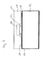
- FIG. 6 shows a highly schematic top view of a fitting frame with inserted and assembled individual cards.
- FIG. 7 shows the carrier structure of FIG. 5 before compression.
- FIG. 8 shows the carrier structure of FIG. 7 after compression.
- FIG. 9 shows the carrier structure of FIG. 8 after the laminated carrier film has been stripped off.
- FIG. 10 shows the carrier structure of FIG. 9 with through-platings.
- FIG. 11 shows the conductor structure element according to the invention after the removal of the rigid carrier.
- FIG. 12 shows an alternative multilayer structure to that shown in FIG. 11 .
- FIG. 13 shows further alternative multilayer structures.
- FIG. 14 shows an exemplary embodiment for a conductor structure element according to the invention with conductors protected by solder stop lacquer.
- FIG. 15 shows a further exemplary embodiment of a conductor structure element according to the invention which is embedded as a “component housing” into a multilayer structure.
- FIG. 16 shows a further exemplary embodiment of a conductor structure element according to the invention.
- FIG. 17 shows a cross-sectional side view of an ultra-thin package according to the invention on a flex substrate.
- FIGS. 18 and 18 a show a cross-sectional side view of a conductor structure element according to the invention in which active chip layers are covered laterally with a permanent etch resist.
- FIG. 19 shows the conductor structure element of FIG. 18 with a back-thinned chip, i.e. a chip with non-active layers removed.
- FIG. 19 a shows in an alternative embodiment to FIG. 19 the conductor structure element of FIG. 18 a with a lower-lying chip after the back-thinning.
- FIG. 20 shows the conductor structure element of FIG. 19 after compression.
- FIG. 20 a shows the conductor structure element of FIG. 19 a after compression.
- FIG. 21 shows the conductor structure element of FIG. 20 after the detachment of the rigid carrier and differential etching.
- FIG. 1 shows a cross-sectional side view of a rigid carrier 12 which essentially has a block-shaped form and in particular has at least one flat surface.
- the rigid carrier 12 is used according to the invention as the basis for applying a multilayer structure.
- the rigid carrier is made of a sufficiently rigid material, as already described at the beginning hereof, in order to prevent as far as possible harmful bending of the layer structure during the further processing of the thin layers to be applied to the carrier.
- the rigid carrier according to the invention must have the material property that it can be detached without damage to the copper layers applied thereon.
- the rigid carrier is a carrier of amphoteric metal such as aluminum, for example, or a suitable aluminum alloy.
- a copper coating 14 is electrodeposited on the carrier. Where applicable, this requires a pretreatment of the rigid carrier, as in the case of aluminum, e.g. a usual zincate treatment.
- a conductive pattern process is carried out on the electrodeposited copper coating 14 , i.e. a conductive pattern structure 16 is applied by photolithography, for example, in the so-called pattern plating process.
- Contact surfaces 18 for components are formed on the conductive pattern structure 16 , where applicable by selective plating, and they may in some cases be provided with a precious metal coating (Au, Ag, NiPdAu, etc.)
- An etch-resistant barrier layer (not shown), for example of Au, Ag, Ni, etc., may be provided between the copper coating 14 and the conductive pattern structure 16 .
- the contact surfaces for components may alternatively be designed as columns 18 ′ with or without component contacts. Due to the greater distance from the conductive pattern structure, the reliability of the connection between the component and the conductor structure is increased in later use, and wafer preparation is simplified. Usually the formation of column structures of this type on thin layers is extremely problematic—with the invention it is possible to provide even the thinnest layers with such contact bumps for components.
- the assembly on the thin conductive pattern layer is also designed to be very simple, since, due to the rigid carrier 12 , a rigid and flat surface to be populated is provided.
- the rigid carrier 12 which is present in a larger format, can be “subdivided” or “individualized”, i.e. divided in its format into individual card formats, e.g. into the so-called “eurocard”, which then after assembly can be replaced in a fitting frame for further (parallel) processing.
- FIG. 6 shows by way of example in schematic top view a fitting frame 100 with inserted individual cards C assembled with components 20 .
- the assembled components can all or in part be underfilled with a suitable material in a manner known per se ( FIG. 5 , reference number 22 ) before (likewise in a manner known per se) compression layers, such as adhesive layers or prepreg layers or the like are applied for compression of the multilayer structure, as is shown schematically in FIG. 7 .
- a full-area prepreg or—as shown in FIG. 1 a first prepreg layer 24 with a recess 26 to accommodate a component 20 and thereon a second full-area prepreg layer 28 can be applied. Due to this procedure a cavity is produced around the component 20 .
- a prepreg layer can be used with a non-through recess, which already forms a cavity.
- the full-area prepreg layer 28 can also be omitted.
- a copper film F can be applied on the upper prepreg layer 28 or 24 , before the entire structure—again in a manner known per se—is compressed.
- resin-coated copper foil so-called RCC foil (Resin Coated Copper) or RCF (Resin Coated Foil) can be used.
- RCC foil Resin Coated Copper
- RCF Resin Coated Foil
- the creation of cavities can be omitted, depending on the component geometry.
- FIG. 8 shows the multilayer structure after the compression with component 20 positively (in form-fitting manner) embedded in a resin layer 28 ′; the resin layer 28 ′ has been produced from the prepreg layers 24 , 28 liquefying during the compression and subsequently solidifying again.
- the copper foil F comprises a somewhat thicker carrier foil 30 (with a thickness in the order of magnitude of 70 ⁇ m) on which, for example, separated by a thin chromium layer, a thinner base copper foil 31 is applied (the thinner foil has a thickness in the order of magnitude of 7 ⁇ m).
- the copper foil F is applied with the thinner base copper foil 31 facing towards the resin layer 28 ′.
- the carrier foil 30 (if present) is peeled off (cf. FIG. 9 ), which likewise proves to be unproblematic due to the rigid substructure of the carrier 12 —otherwise it would be hard to easily peel a carrier foil off a thin layer.
- the carrier foil 30 has been peeled off, the much thinner base copper foil 31 remains on the mutlilayer structure.
- further processing possibilities are now opened up for the mutlilayer structure according to the invention.
- FIG. 10 shows, for example, the possibility of producing a blind hole 36 on the surface of the component 20 and/or a blind hole 34 on the plane of the conductive pattern structure 16 for the purpose of contacting.
- the chip or the component 20 should have an electroplating-compatible surface.
- the boring can be carried out, for example, by laser drilling, with subsequent plating to produce a continuous copper layer 32 (the copper layer 32 is composed of the laminated base copper foil 31 plus copper electrodeposited thereon).
- the blind holes 36 for contacting of the component 20 are completely filled with copper, while the walls of the blind hole 34 for contacting of the conductor paths are coated with copper.
- the rigid carrier 12 is removed. This is carried out by dissolving or etching of the rigid carrier 12 in a suitable medium; in the case of aluminum this would be caustic soda, for example. If necessary, before the detachment of the rigid carrier 12 , an etching step for etching the “base copper,” that is, the copper plating 14 of the carrier 12 on the underside (as shown in the figure) of the carrier is carried out, followed by selective etching of the rigid carrier 12 , and finally by removal of the copper coating 14 on the underside of the multilayer structure, for example, by differential etching, thereby exposing the conductive pattern structure 16 . In the course of this, individual points of the copper layer 32 (cf. reference number 38 ) and of the copper layer 14 (not shown) can also be selectively etched.
- “Differential etching” here means an etching process in which an etching medium dissolves the copper (here: copper coating 14 ), but does not thereby remove or only slightly removes the underlying structure (here: conductive pattern structure 16 ). This requires a precise control of the etching depth and permits removal of the top layer without using etch resist. If, for example, given a layer thickness of approx. 5 ⁇ m of the (top) layer (copper coating 14 ) to be removed, etching is carried out by differential etching to approx. 7 ⁇ m in depth, then the top layer will be completely removed, while the underlying layer (the conductive pattern structure) will be reduced in thickness by only approx. 2 ⁇ m.
- the structures (“packages”) produced can still be processed even after the removal of the rigid carrier 12 , for example, by generating through platings 40 by means of drilling (laser, mechanical, plasma) and subsequent plating with copper.
- the conductive pattern structures 16 are embedded in the resin layer 28 ′, i.e. they do not project.
- the plating of the layer 42 is carried out before the removal and/or possible differential etching of the copper coating 14 . Exposed conductors can be protected by solder stop lacquer 46 (cf. FIG. 14 ).
- the conductive pattern structure 16 is “exposed,” that is, the structure of the conductive pattern with the layer sequence 16 - 14 - 42 becomes visible again, in that the intervening copper-coated regions (copper coating 14 and optionally copper layer 42 ) are etched.
- the coating ( 14 ; 42 ) on the actual conductive pattern layer 16 can also be at least partially etched and/or further platings can also be carried out (for example, in the case of the stepped conductor 44 described).
- FIG. 15 shows a further field of application of the invention.
- a component 70 shown by a broken line prefabricated according to the invention is laminated into a multilayer structure of a printed circuit board B.
- the electrical connection to the printed circuit board B is made by drilling through the conductive pattern structure 16 at the positions provided for this purpose and metallizing these boreholes using processes that are conventional in circuit board technology (copper layer 48 ).
- copper layer 48 In order to ensure a reliable metallic connection of the through-platings 40 to the conductive pattern structure 16 , it is advantageous to make them of pure copper.
- the layer sequence known from RU 2291598 C2 is not suitable for a process of this type.
- FIG. 16 shows a further exemplary embodiment in which additional layers (for example FR-4 or RCC layers 28 ′′) are laminated and corresponding additional planes of conductor paths 50 with corresponding through-platings 42 can be formed.
- additional layers for example FR-4 or RCC layers 28 ′′
- FIG. 17 shows an ultra-thin package 10 according to the invention on a so-called flexible flex substrate 60 .
- the electrical contact between the flexible carrier PCB and the conductive pattern structure 16 of the thin component is in this case achieved via metallized holes 62 which are produced, e. g. by laser erosion and are copper plated by means of conventional metallization processes.
- the ultra-thin package 10 is adhesively laminated with the flex substrate 60 , the holes 62 are produced and subsequently metallized.
- the electrical connection between the conductor structure element 10 and the flex substrate 60 is thus made via the metallization of the holes 62 .
- These holes 62 (as shown in the figure) can be designed as blind holes extending to the conductor path 16 . However, they can also be designed as through-holes (not shown). This results according to the invention in a thin electronic assembly that does not have to be soldered.
- FIG. 18 shows a further exemplary embodiment of a multilayer structure according to the invention before the removal of the rigid carrier 12 .
- the etch resist layer 54 has a height that is selected such that it covers active layers 20 . 1 at the bottom of the chip 20 (as shown in the figure), around the sawn edges thereof, namely at the level of the layer transition region. By this is meant the location of the chip 20 at which active and inactive layers meet (shown as a dashed line in FIG. 18 ).
- the etch resist layer 54 is thus applied thickly enough that it laterally covers the chip at least up to the height of this point. However, it can also be applied more thickly and thus laterally cover the chip to a point higher than the layer transition region.
- materials can be used which are temporarily used for the etching process and thereafter are removed again, or materials are used which are etch-resistant and due to their material properties can remain in the structure.
- etch resist layer 54 naturally suggests a chemical removal of the inactive chip layers 20 . 2 . This is carried out by means of etching. Between the active layers 20 . 1 and the non-active (silicon) layers 20 . 2 of the chip 20 a layer 21 of etch-resistant material is provided (which in principle corresponds to the dashed line in FIG. 18 and in principle represents the layer transition region described above), whereby the etching process is facilitated, since it ends automatically when the etch-resistant layer 21 is reached. The chip 20 thus eroded down to its active layer 20 .
- etch resist layer 54 thus joins flush with the surface of the etch resist layer 54 or may even be located somewhat lower than it, if the etch resist layer 54 , as explained above, has been applied higher than the active layers 20 . 1 of the chip 20 (cf. FIG. 18 a ).
- the etch resist layer 54 as shown in FIG. 18 a as well as in FIGS. 19 a and 20 a —can alternatively be used to underfill the chip or it can be used in combination with a separately provided underfilling (reference number 22 in FIGS. 18, 19 and 20 ).
- FIGS. 19 a and 20 a respectively show the embodiment with the chemically back-thinned chip 20 in a lower position compared to the level of the etch resist layer 54 .
- a next step (cf. FIG. 21 ), the detachment of the rigid carrier 12 is carried out as well as differential etching of the copper coating 14 , as well as optionally further processing (as also already described above in connection with FIGS. 11 through 17 , i.e. for example, provision of contacting and/or through-platings, lamination in a multilayer structure, use as interposer, etc.)
- the structure shown in FIG. 20 can alternatively also be inserted in a multilayer structure before the detachment of the rigid carrier or it can be compressed with a further multilayer structure according to the invention with a rigid carrier in a sandwich structure so that the two rigid carriers respectively come to rest on the outside (at the top and bottom in figure) and finally can be dissolved or detached in a common etching process. Before the detachment process, further measures for further processing can be carried out.
- detachment of the rigid carrier 12 can first be carried out and then be followed by lamination into a printed circuit board. Since the eroded chip 20 is now flush with the surface of the etch resist 54 , or optionally is situated even somewhat lower, the formation of cavities in prepregs of a multilayer can be omitted.
- the chip thickness or chip height can be restricted to the active layers 20 . 1 and is therefore very thin, at approx. 10 ⁇ m, depending on the chip design.
- a total thickness of the multilayer structure shown in FIG. 21 of approx. 100 ⁇ m can thus be achieved.
- the detachment of the non-active silicon (layers 20 . 2 ) from the back of the chip 20 could also be facilitated by a modified production of the chip 20 itself: Before the production of the first active layers 20 . 1 , an etch-resistant layer is deposited on a wafer. Epitaxial layers can subsequently be deposited on this etch-resistant layer, from which then successively the active layers 20 . 1 of the chip 20 are produced. The wafer is thereby used as a carrier for the active layers 20 . 1
- the carrier silicon could now be completely etched off with an etching medium.
Landscapes
- Engineering & Computer Science (AREA)
- Manufacturing & Machinery (AREA)
- Microelectronics & Electronic Packaging (AREA)
- Production Of Multi-Layered Print Wiring Board (AREA)
- Ceramic Engineering (AREA)
Abstract
Description
Claims (20)
Applications Claiming Priority (4)
| Application Number | Priority Date | Filing Date | Title |
|---|---|---|---|
| DE102009060480.4 | 2009-12-18 | ||
| DE102009060480A DE102009060480A1 (en) | 2009-12-18 | 2009-12-18 | Conductor structure element and method for producing a conductor structure element |
| DE102009060480 | 2009-12-18 | ||
| PCT/EP2010/007736 WO2011079918A2 (en) | 2009-12-18 | 2010-12-17 | Conductor structural element and method for producing a conductor structural element |
Publications (2)
| Publication Number | Publication Date |
|---|---|
| US20120320549A1 US20120320549A1 (en) | 2012-12-20 |
| US9456500B2 true US9456500B2 (en) | 2016-09-27 |
Family
ID=43795825
Family Applications (1)
| Application Number | Title | Priority Date | Filing Date |
|---|---|---|---|
| US13/515,012 Active 2033-12-31 US9456500B2 (en) | 2009-12-18 | 2010-12-17 | Conductor structure element and method for producing a conductor structure element |
Country Status (6)
| Country | Link |
|---|---|
| US (1) | US9456500B2 (en) |
| EP (2) | EP2814306A1 (en) |
| JP (2) | JP2013514637A (en) |
| CN (1) | CN102763494B (en) |
| DE (2) | DE102009060480A1 (en) |
| WO (1) | WO2011079918A2 (en) |
Cited By (2)
| Publication number | Priority date | Publication date | Assignee | Title |
|---|---|---|---|---|
| DE102019208093A1 (en) * | 2019-06-04 | 2020-12-10 | Robert Bosch Gmbh | Method for producing a three-dimensional circuit and three-dimensional circuit |
| US11569195B2 (en) * | 2019-03-15 | 2023-01-31 | Kore Semiconductor Co., Ltd. | Semiconductor packaging structure and method of fabricating same |
Families Citing this family (9)
| Publication number | Priority date | Publication date | Assignee | Title |
|---|---|---|---|---|
| US10043707B2 (en) * | 2012-10-16 | 2018-08-07 | Qorvo Us, Inc. | Additive conductor redistribution layer (ACRL) |
| US9627338B2 (en) * | 2013-03-06 | 2017-04-18 | STATS ChipPAC Pte. Ltd. | Semiconductor device and method of forming ultra high density embedded semiconductor die package |
| CN103182608B (en) * | 2013-04-03 | 2015-12-23 | 大族激光科技产业集团股份有限公司 | The processing method that pcb board is uncapped |
| KR102231101B1 (en) * | 2014-11-18 | 2021-03-23 | 삼성전기주식회사 | Element embedded printed circuit board and method of manufacturing the same |
| DE102015113322B3 (en) | 2015-08-12 | 2016-11-17 | Schweizer Electronic Ag | Radio-frequency antenna, radio-frequency substrate with radio-frequency antenna and method of production |
| CN109152230A (en) * | 2018-08-28 | 2019-01-04 | 上海幂方电子科技有限公司 | Flexible circuit and its manufacturing method |
| CN109413891B (en) * | 2018-11-20 | 2020-12-22 | 广东依顿电子科技股份有限公司 | Blind hole circuit board and manufacturing method thereof |
| CN111372369B (en) | 2018-12-25 | 2023-07-07 | 奥特斯科技(重庆)有限公司 | Component carrier with component shielding and method for producing the same |
| DE102019132852B4 (en) * | 2019-12-03 | 2021-12-30 | Schweizer Electronic Ag | Method for producing a conductor structure element and conductor structure element |
Citations (19)
| Publication number | Priority date | Publication date | Assignee | Title |
|---|---|---|---|---|
| US2692190A (en) | 1953-08-17 | 1954-10-19 | Pritikin Nathan | Method of making inlaid circuits |
| GB1005943A (en) | 1962-10-18 | 1965-09-29 | Intellux Inc | Multilayer electrical circuit assemblies and processes for producing such assemblies |
| DE2242132B2 (en) | 1971-08-30 | 1975-08-07 | Perstorp Ab, Perstorp (Schweden) | Process for the production of a plated through-hole printed circuit board |
| US4354895A (en) | 1981-11-27 | 1982-10-19 | International Business Machines Corporation | Method for making laminated multilayer circuit boards |
| JPS62158336A (en) | 1985-12-31 | 1987-07-14 | Casio Comput Co Ltd | Mounting structure of electronic parts and their mounting method |
| JPH06350234A (en) | 1992-10-16 | 1994-12-22 | Ameg Additive Metallisierung Entwickl & Anwendungs Gmbh | Method for attaching and contacting electrical and / or electronic components to an insulating substrate, method for manufacturing printed wiring board by currentless metal deposition, and method for attaching and contacting electronic components |
| JPH07202424A (en) | 1993-12-28 | 1995-08-04 | Nec Corp | Production of multilayer wiring board |
| JP2001085286A (en) | 1999-09-13 | 2001-03-30 | Seiko Epson Corp | Semiconductor chip manufacturing method, circuit board, and electronic device |
| JP2001177004A (en) | 1999-12-17 | 2001-06-29 | Shinko Electric Ind Co Ltd | Multilayer wiring board, method for manufacturing multilayer wiring board, and semiconductor device |
| JP2001203482A (en) | 2000-01-21 | 2001-07-27 | Hitachi Kokusai Electric Inc | Removable printed circuit board mounting frame |
| JP2001274324A (en) | 2000-03-24 | 2001-10-05 | Hitachi Chem Co Ltd | Semiconductor mounting substrate for stacked semiconductor device, semiconductor device, and stacked semiconductor device |
| US20020039808A1 (en) | 1994-03-18 | 2002-04-04 | Hitachi Chemical Company, Ltd. | Fabrication process of semiconductor package and semiconductor package |
| JP2003289128A (en) | 2002-01-23 | 2003-10-10 | Matsushita Electric Ind Co Ltd | Circuit component built-in module and method of manufacturing the same |
| JP2003298213A (en) | 2002-04-03 | 2003-10-17 | Matsushita Electric Ind Co Ltd | Printed wiring board and its manufacturing method |
| JP2005086071A (en) | 2003-09-10 | 2005-03-31 | Hitachi Chem Co Ltd | Multilayer wiring substrate, semiconductor chip mounting substrate, semiconductor package, and manufacturing method thereof |
| DE102005032489B3 (en) | 2005-07-04 | 2006-11-16 | Schweizer Electronic Ag | Circuit board multi-layer structure with integrated electric component, has insert embedded between two flat electrically insulating liquid resin structures |
| US7268012B2 (en) * | 2004-08-31 | 2007-09-11 | Micron Technology, Inc. | Methods for fabrication of thin semiconductor assemblies including redistribution layers and packages and assemblies formed thereby |
| JP2007276319A (en) | 2006-04-07 | 2007-10-25 | Dainippon Printing Co Ltd | Substrate pressing auxiliary plate, wiring board unit manufacturing apparatus and wiring board unit manufacturing method. |
| WO2009118925A1 (en) | 2008-03-27 | 2009-10-01 | イビデン株式会社 | Circuit board having built-in electronic parts and its manufacturing method |
Family Cites Families (11)
| Publication number | Priority date | Publication date | Assignee | Title |
|---|---|---|---|---|
| JPS5670655A (en) * | 1979-11-15 | 1981-06-12 | Matsushita Electric Ind Co Ltd | Manufacture of electronic circuit mounting device |
| EP0256778A3 (en) * | 1986-08-08 | 1989-03-08 | Ronald Krajewski | Multi-layer printed circuit structure |
| KR100274764B1 (en) * | 1991-11-29 | 2001-01-15 | 이사오 우치가사키 | Manufacturing method of the wiring board |
| TW569424B (en) * | 2000-03-17 | 2004-01-01 | Matsushita Electric Industrial Co Ltd | Module with embedded electric elements and the manufacturing method thereof |
| JP2003152021A (en) * | 2001-11-09 | 2003-05-23 | Seiko Epson Corp | Semiconductor device and its manufacturing method, circuit board, and electronic equipment |
| TW200302685A (en) * | 2002-01-23 | 2003-08-01 | Matsushita Electric Industrial Co Ltd | Circuit component built-in module and method of manufacturing the same |
| JP2003304065A (en) * | 2002-04-08 | 2003-10-24 | Sony Corp | Circuit board device and its manufacturing method, and semiconductor device and its manufacturing method |
| US6946205B2 (en) * | 2002-04-25 | 2005-09-20 | Matsushita Electric Industrial Co., Ltd. | Wiring transfer sheet and method for producing the same, and wiring board and method for producing the same |
| US6898850B2 (en) * | 2002-08-06 | 2005-05-31 | Matsushita Electric Industrial Co., Ltd. | Method of manufacturing circuit board and communication appliance |
| JP4461912B2 (en) * | 2004-06-08 | 2010-05-12 | 日立化成工業株式会社 | Manufacturing method of multilayer printed wiring board |
| RU2291598C2 (en) | 2005-02-08 | 2007-01-10 | Федеральное государственное унитарное предприятие "Научно-производственное предприятие "Полет" | Method for making flexible multi-layer electronic boards |
-
2009
- 2009-12-18 DE DE102009060480A patent/DE102009060480A1/en not_active Withdrawn
-
2010
- 2010-12-17 CN CN201080064300.6A patent/CN102763494B/en not_active Expired - Fee Related
- 2010-12-17 WO PCT/EP2010/007736 patent/WO2011079918A2/en not_active Ceased
- 2010-12-17 EP EP20140002625 patent/EP2814306A1/en not_active Withdrawn
- 2010-12-17 DE DE202010017809U patent/DE202010017809U1/en not_active Expired - Lifetime
- 2010-12-17 JP JP2012543532A patent/JP2013514637A/en active Pending
- 2010-12-17 EP EP10803568.4A patent/EP2415332B1/en not_active Not-in-force
- 2010-12-17 US US13/515,012 patent/US9456500B2/en active Active
-
2015
- 2015-11-13 JP JP2015223125A patent/JP2016048795A/en not_active Withdrawn
Patent Citations (21)
| Publication number | Priority date | Publication date | Assignee | Title |
|---|---|---|---|---|
| US2692190A (en) | 1953-08-17 | 1954-10-19 | Pritikin Nathan | Method of making inlaid circuits |
| GB1005943A (en) | 1962-10-18 | 1965-09-29 | Intellux Inc | Multilayer electrical circuit assemblies and processes for producing such assemblies |
| DE2242132B2 (en) | 1971-08-30 | 1975-08-07 | Perstorp Ab, Perstorp (Schweden) | Process for the production of a plated through-hole printed circuit board |
| US4354895A (en) | 1981-11-27 | 1982-10-19 | International Business Machines Corporation | Method for making laminated multilayer circuit boards |
| JPS62158336A (en) | 1985-12-31 | 1987-07-14 | Casio Comput Co Ltd | Mounting structure of electronic parts and their mounting method |
| JPH06350234A (en) | 1992-10-16 | 1994-12-22 | Ameg Additive Metallisierung Entwickl & Anwendungs Gmbh | Method for attaching and contacting electrical and / or electronic components to an insulating substrate, method for manufacturing printed wiring board by currentless metal deposition, and method for attaching and contacting electronic components |
| JPH07202424A (en) | 1993-12-28 | 1995-08-04 | Nec Corp | Production of multilayer wiring board |
| US20020039808A1 (en) | 1994-03-18 | 2002-04-04 | Hitachi Chemical Company, Ltd. | Fabrication process of semiconductor package and semiconductor package |
| JP2001085286A (en) | 1999-09-13 | 2001-03-30 | Seiko Epson Corp | Semiconductor chip manufacturing method, circuit board, and electronic device |
| JP2001177004A (en) | 1999-12-17 | 2001-06-29 | Shinko Electric Ind Co Ltd | Multilayer wiring board, method for manufacturing multilayer wiring board, and semiconductor device |
| JP2001203482A (en) | 2000-01-21 | 2001-07-27 | Hitachi Kokusai Electric Inc | Removable printed circuit board mounting frame |
| JP2001274324A (en) | 2000-03-24 | 2001-10-05 | Hitachi Chem Co Ltd | Semiconductor mounting substrate for stacked semiconductor device, semiconductor device, and stacked semiconductor device |
| JP2003289128A (en) | 2002-01-23 | 2003-10-10 | Matsushita Electric Ind Co Ltd | Circuit component built-in module and method of manufacturing the same |
| JP2003298213A (en) | 2002-04-03 | 2003-10-17 | Matsushita Electric Ind Co Ltd | Printed wiring board and its manufacturing method |
| JP2005086071A (en) | 2003-09-10 | 2005-03-31 | Hitachi Chem Co Ltd | Multilayer wiring substrate, semiconductor chip mounting substrate, semiconductor package, and manufacturing method thereof |
| US7268012B2 (en) * | 2004-08-31 | 2007-09-11 | Micron Technology, Inc. | Methods for fabrication of thin semiconductor assemblies including redistribution layers and packages and assemblies formed thereby |
| DE102005032489B3 (en) | 2005-07-04 | 2006-11-16 | Schweizer Electronic Ag | Circuit board multi-layer structure with integrated electric component, has insert embedded between two flat electrically insulating liquid resin structures |
| JP2007276319A (en) | 2006-04-07 | 2007-10-25 | Dainippon Printing Co Ltd | Substrate pressing auxiliary plate, wiring board unit manufacturing apparatus and wiring board unit manufacturing method. |
| WO2009118925A1 (en) | 2008-03-27 | 2009-10-01 | イビデン株式会社 | Circuit board having built-in electronic parts and its manufacturing method |
| US20090242255A1 (en) | 2008-03-27 | 2009-10-01 | Ibiden Co., Ltd | Wiring board with built-in electronic component and method of manufacturing same |
| US8347493B2 (en) * | 2008-03-27 | 2013-01-08 | Ibiden Co., Ltd. | Wiring board with built-in electronic component and method of manufacturing same |
Cited By (2)
| Publication number | Priority date | Publication date | Assignee | Title |
|---|---|---|---|---|
| US11569195B2 (en) * | 2019-03-15 | 2023-01-31 | Kore Semiconductor Co., Ltd. | Semiconductor packaging structure and method of fabricating same |
| DE102019208093A1 (en) * | 2019-06-04 | 2020-12-10 | Robert Bosch Gmbh | Method for producing a three-dimensional circuit and three-dimensional circuit |
Also Published As
| Publication number | Publication date |
|---|---|
| CN102763494A (en) | 2012-10-31 |
| WO2011079918A3 (en) | 2011-10-13 |
| JP2013514637A (en) | 2013-04-25 |
| DE202010017809U1 (en) | 2012-11-15 |
| EP2415332B1 (en) | 2014-07-30 |
| CN102763494B (en) | 2015-11-25 |
| EP2415332A2 (en) | 2012-02-08 |
| US20120320549A1 (en) | 2012-12-20 |
| JP2016048795A (en) | 2016-04-07 |
| DE102009060480A1 (en) | 2011-06-22 |
| EP2814306A1 (en) | 2014-12-17 |
| WO2011079918A2 (en) | 2011-07-07 |
Similar Documents
| Publication | Publication Date | Title |
|---|---|---|
| US9456500B2 (en) | Conductor structure element and method for producing a conductor structure element | |
| CN101683004B (en) | Method for manufacturing multilayer printed wiring board | |
| CN1835654B (en) | Wiring board and method of manufacturing the same | |
| CN106409688B (en) | A kind of processing method and structure of ultra-thin centreless package substrate | |
| US8461460B2 (en) | Microelectronic interconnect element with decreased conductor spacing | |
| JP5107187B2 (en) | Manufacturing method of electronic component package | |
| KR20120093776A (en) | Method of manufacturing multilayer wiring substrate | |
| CN106340461B (en) | A kind of processing method and structure of ultra-thin centreless package substrate | |
| JP4143609B2 (en) | Wiring board manufacturing method | |
| KR20160032985A (en) | Package board, method for manufacturing the same and package on package having the thereof | |
| CN110211943A (en) | Semiconductor device and its manufacturing method | |
| JP2012084826A (en) | Method of manufacturing semiconductor package | |
| JP4332162B2 (en) | Wiring board manufacturing method | |
| US12040272B2 (en) | Connector for implementing multi-faceted interconnection | |
| JP2016134622A (en) | Embedded board and method of manufacturing embedded board | |
| KR20160004158A (en) | Package substrate | |
| JP4549692B2 (en) | Wiring board manufacturing method | |
| JP4549694B2 (en) | Wiring substrate manufacturing method and multi-cavity substrate | |
| KR100796981B1 (en) | Printed Circuit Board Manufacturing Method | |
| JP4580752B2 (en) | Manufacturing method of semiconductor device | |
| JP5458398B2 (en) | Electronic component package manufacturing method and electronic component package | |
| JP2016225443A (en) | Manufacturing method of printed wiring board | |
| JP2005079108A (en) | Wiring board manufacturing method | |
| JP2005235980A (en) | Wiring board manufacturing method, wiring board, and semiconductor package | |
| JP2008021944A (en) | Multilayer wiring board and manufacturing method thereof |
Legal Events
| Date | Code | Title | Description |
|---|---|---|---|
| AS | Assignment |
Owner name: SCHWEIZER ELECTRONIC AG, GERMANY Free format text: ASSIGNMENT OF ASSIGNORS INTEREST;ASSIGNORS:GOTTWALD, THOMAS;NEUMANN, ALEXANDER;REEL/FRAME:028737/0330 Effective date: 20120712 |
|
| STCF | Information on status: patent grant |
Free format text: PATENTED CASE |
|
| MAFP | Maintenance fee payment |
Free format text: PAYMENT OF MAINTENANCE FEE, 4TH YEAR, LARGE ENTITY (ORIGINAL EVENT CODE: M1551); ENTITY STATUS OF PATENT OWNER: LARGE ENTITY Year of fee payment: 4 |
|
| MAFP | Maintenance fee payment |
Free format text: PAYMENT OF MAINTENANCE FEE, 8TH YEAR, LARGE ENTITY (ORIGINAL EVENT CODE: M1552); ENTITY STATUS OF PATENT OWNER: LARGE ENTITY Year of fee payment: 8 |