US9411470B2 - Light sensitive display with multiple data set object detection - Google Patents
Light sensitive display with multiple data set object detection Download PDFInfo
- Publication number
- US9411470B2 US9411470B2 US12/568,302 US56830209A US9411470B2 US 9411470 B2 US9411470 B2 US 9411470B2 US 56830209 A US56830209 A US 56830209A US 9411470 B2 US9411470 B2 US 9411470B2
- Authority
- US
- United States
- Prior art keywords
- light
- display
- sensitive elements
- light sensitive
- display device
- Prior art date
- Legal status (The legal status is an assumption and is not a legal conclusion. Google has not performed a legal analysis and makes no representation as to the accuracy of the status listed.)
- Expired - Fee Related, expires
Links
Images


Classifications
-
- G—PHYSICS
- G06—COMPUTING OR CALCULATING; COUNTING
- G06F—ELECTRIC DIGITAL DATA PROCESSING
- G06F3/00—Input arrangements for transferring data to be processed into a form capable of being handled by the computer; Output arrangements for transferring data from processing unit to output unit, e.g. interface arrangements
- G06F3/01—Input arrangements or combined input and output arrangements for interaction between user and computer
- G06F3/03—Arrangements for converting the position or the displacement of a member into a coded form
- G06F3/041—Digitisers, e.g. for touch screens or touch pads, characterised by the transducing means
- G06F3/042—Digitisers, e.g. for touch screens or touch pads, characterised by the transducing means by opto-electronic means
-
- G—PHYSICS
- G02—OPTICS
- G02F—OPTICAL DEVICES OR ARRANGEMENTS FOR THE CONTROL OF LIGHT BY MODIFICATION OF THE OPTICAL PROPERTIES OF THE MEDIA OF THE ELEMENTS INVOLVED THEREIN; NON-LINEAR OPTICS; FREQUENCY-CHANGING OF LIGHT; OPTICAL LOGIC ELEMENTS; OPTICAL ANALOGUE/DIGITAL CONVERTERS
- G02F1/00—Devices or arrangements for the control of the intensity, colour, phase, polarisation or direction of light arriving from an independent light source, e.g. switching, gating or modulating; Non-linear optics
- G02F1/01—Devices or arrangements for the control of the intensity, colour, phase, polarisation or direction of light arriving from an independent light source, e.g. switching, gating or modulating; Non-linear optics for the control of the intensity, phase, polarisation or colour
- G02F1/13—Devices or arrangements for the control of the intensity, colour, phase, polarisation or direction of light arriving from an independent light source, e.g. switching, gating or modulating; Non-linear optics for the control of the intensity, phase, polarisation or colour based on liquid crystals, e.g. single liquid crystal display cells
- G02F1/133—Constructional arrangements; Operation of liquid crystal cells; Circuit arrangements
- G02F1/1333—Constructional arrangements; Manufacturing methods
- G02F1/13338—Input devices, e.g. touch panels
-
- G—PHYSICS
- G06—COMPUTING OR CALCULATING; COUNTING
- G06F—ELECTRIC DIGITAL DATA PROCESSING
- G06F1/00—Details not covered by groups G06F3/00 - G06F13/00 and G06F21/00
- G06F1/16—Constructional details or arrangements
- G06F1/1601—Constructional details related to the housing of computer displays, e.g. of CRT monitors, of flat displays
- G06F1/1607—Arrangements to support accessories mechanically attached to the display housing
- G06F1/1611—Arrangements to support accessories mechanically attached to the display housing to support document holders
-
- G—PHYSICS
- G06—COMPUTING OR CALCULATING; COUNTING
- G06F—ELECTRIC DIGITAL DATA PROCESSING
- G06F3/00—Input arrangements for transferring data to be processed into a form capable of being handled by the computer; Output arrangements for transferring data from processing unit to output unit, e.g. interface arrangements
- G06F3/01—Input arrangements or combined input and output arrangements for interaction between user and computer
- G06F3/03—Arrangements for converting the position or the displacement of a member into a coded form
- G06F3/033—Pointing devices displaced or positioned by the user, e.g. mice, trackballs, pens or joysticks; Accessories therefor
- G06F3/0354—Pointing devices displaced or positioned by the user, e.g. mice, trackballs, pens or joysticks; Accessories therefor with detection of two-dimensional [2D] relative movements between the device, or an operating part thereof, and a plane or surface, e.g. 2D mice, trackballs, pens or pucks
- G06F3/03542—Light pens for emitting or receiving light
-
- G—PHYSICS
- G06—COMPUTING OR CALCULATING; COUNTING
- G06F—ELECTRIC DIGITAL DATA PROCESSING
- G06F3/00—Input arrangements for transferring data to be processed into a form capable of being handled by the computer; Output arrangements for transferring data from processing unit to output unit, e.g. interface arrangements
- G06F3/01—Input arrangements or combined input and output arrangements for interaction between user and computer
- G06F3/03—Arrangements for converting the position or the displacement of a member into a coded form
- G06F3/033—Pointing devices displaced or positioned by the user, e.g. mice, trackballs, pens or joysticks; Accessories therefor
- G06F3/0354—Pointing devices displaced or positioned by the user, e.g. mice, trackballs, pens or joysticks; Accessories therefor with detection of two-dimensional [2D] relative movements between the device, or an operating part thereof, and a plane or surface, e.g. 2D mice, trackballs, pens or pucks
- G06F3/03545—Pens or stylus
-
- G—PHYSICS
- G06—COMPUTING OR CALCULATING; COUNTING
- G06F—ELECTRIC DIGITAL DATA PROCESSING
- G06F3/00—Input arrangements for transferring data to be processed into a form capable of being handled by the computer; Output arrangements for transferring data from processing unit to output unit, e.g. interface arrangements
- G06F3/01—Input arrangements or combined input and output arrangements for interaction between user and computer
- G06F3/03—Arrangements for converting the position or the displacement of a member into a coded form
- G06F3/041—Digitisers, e.g. for touch screens or touch pads, characterised by the transducing means
- G06F3/0412—Digitisers structurally integrated in a display
-
- G—PHYSICS
- G06—COMPUTING OR CALCULATING; COUNTING
- G06F—ELECTRIC DIGITAL DATA PROCESSING
- G06F3/00—Input arrangements for transferring data to be processed into a form capable of being handled by the computer; Output arrangements for transferring data from processing unit to output unit, e.g. interface arrangements
- G06F3/01—Input arrangements or combined input and output arrangements for interaction between user and computer
- G06F3/03—Arrangements for converting the position or the displacement of a member into a coded form
- G06F3/041—Digitisers, e.g. for touch screens or touch pads, characterised by the transducing means
- G06F3/0416—Control or interface arrangements specially adapted for digitisers
- G06F3/0418—Control or interface arrangements specially adapted for digitisers for error correction or compensation, e.g. based on parallax, calibration or alignment
-
- G—PHYSICS
- G06—COMPUTING OR CALCULATING; COUNTING
- G06F—ELECTRIC DIGITAL DATA PROCESSING
- G06F3/00—Input arrangements for transferring data to be processed into a form capable of being handled by the computer; Output arrangements for transferring data from processing unit to output unit, e.g. interface arrangements
- G06F3/01—Input arrangements or combined input and output arrangements for interaction between user and computer
- G06F3/03—Arrangements for converting the position or the displacement of a member into a coded form
- G06F3/041—Digitisers, e.g. for touch screens or touch pads, characterised by the transducing means
- G06F3/042—Digitisers, e.g. for touch screens or touch pads, characterised by the transducing means by opto-electronic means
- G06F3/0421—Digitisers, e.g. for touch screens or touch pads, characterised by the transducing means by opto-electronic means by interrupting or reflecting a light beam, e.g. optical touch-screen
-
- G—PHYSICS
- G06—COMPUTING OR CALCULATING; COUNTING
- G06F—ELECTRIC DIGITAL DATA PROCESSING
- G06F3/00—Input arrangements for transferring data to be processed into a form capable of being handled by the computer; Output arrangements for transferring data from processing unit to output unit, e.g. interface arrangements
- G06F3/01—Input arrangements or combined input and output arrangements for interaction between user and computer
- G06F3/048—Interaction techniques based on graphical user interfaces [GUI]
- G06F3/0487—Interaction techniques based on graphical user interfaces [GUI] using specific features provided by the input device, e.g. functions controlled by the rotation of a mouse with dual sensing arrangements, or of the nature of the input device, e.g. tap gestures based on pressure sensed by a digitiser
- G06F3/0488—Interaction techniques based on graphical user interfaces [GUI] using specific features provided by the input device, e.g. functions controlled by the rotation of a mouse with dual sensing arrangements, or of the nature of the input device, e.g. tap gestures based on pressure sensed by a digitiser using a touch-screen or digitiser, e.g. input of commands through traced gestures
-
- G06K9/0004—
-
- G—PHYSICS
- G06—COMPUTING OR CALCULATING; COUNTING
- G06V—IMAGE OR VIDEO RECOGNITION OR UNDERSTANDING
- G06V40/00—Recognition of biometric, human-related or animal-related patterns in image or video data
- G06V40/10—Human or animal bodies, e.g. vehicle occupants or pedestrians; Body parts, e.g. hands
- G06V40/12—Fingerprints or palmprints
- G06V40/13—Sensors therefor
- G06V40/1318—Sensors therefor using electro-optical elements or layers, e.g. electroluminescent sensing
-
- G—PHYSICS
- G09—EDUCATION; CRYPTOGRAPHY; DISPLAY; ADVERTISING; SEALS
- G09G—ARRANGEMENTS OR CIRCUITS FOR CONTROL OF INDICATING DEVICES USING STATIC MEANS TO PRESENT VARIABLE INFORMATION
- G09G3/00—Control arrangements or circuits, of interest only in connection with visual indicators other than cathode-ray tubes
- G09G3/20—Control arrangements or circuits, of interest only in connection with visual indicators other than cathode-ray tubes for presentation of an assembly of a number of characters, e.g. a page, by composing the assembly by combination of individual elements arranged in a matrix no fixed position being assigned to or needed to be assigned to the individual characters or partial characters
- G09G3/34—Control arrangements or circuits, of interest only in connection with visual indicators other than cathode-ray tubes for presentation of an assembly of a number of characters, e.g. a page, by composing the assembly by combination of individual elements arranged in a matrix no fixed position being assigned to or needed to be assigned to the individual characters or partial characters by control of light from an independent source
- G09G3/36—Control arrangements or circuits, of interest only in connection with visual indicators other than cathode-ray tubes for presentation of an assembly of a number of characters, e.g. a page, by composing the assembly by combination of individual elements arranged in a matrix no fixed position being assigned to or needed to be assigned to the individual characters or partial characters by control of light from an independent source using liquid crystals
- G09G3/3611—Control of matrices with row and column drivers
- G09G3/3648—Control of matrices with row and column drivers using an active matrix
-
- G—PHYSICS
- G02—OPTICS
- G02F—OPTICAL DEVICES OR ARRANGEMENTS FOR THE CONTROL OF LIGHT BY MODIFICATION OF THE OPTICAL PROPERTIES OF THE MEDIA OF THE ELEMENTS INVOLVED THEREIN; NON-LINEAR OPTICS; FREQUENCY-CHANGING OF LIGHT; OPTICAL LOGIC ELEMENTS; OPTICAL ANALOGUE/DIGITAL CONVERTERS
- G02F1/00—Devices or arrangements for the control of the intensity, colour, phase, polarisation or direction of light arriving from an independent light source, e.g. switching, gating or modulating; Non-linear optics
- G02F1/01—Devices or arrangements for the control of the intensity, colour, phase, polarisation or direction of light arriving from an independent light source, e.g. switching, gating or modulating; Non-linear optics for the control of the intensity, phase, polarisation or colour
- G02F1/13—Devices or arrangements for the control of the intensity, colour, phase, polarisation or direction of light arriving from an independent light source, e.g. switching, gating or modulating; Non-linear optics for the control of the intensity, phase, polarisation or colour based on liquid crystals, e.g. single liquid crystal display cells
- G02F1/133—Constructional arrangements; Operation of liquid crystal cells; Circuit arrangements
- G02F1/13306—Circuit arrangements or driving methods for the control of single liquid crystal cells
- G02F1/13312—Circuits comprising photodetectors for purposes other than feedback
-
- G—PHYSICS
- G02—OPTICS
- G02F—OPTICAL DEVICES OR ARRANGEMENTS FOR THE CONTROL OF LIGHT BY MODIFICATION OF THE OPTICAL PROPERTIES OF THE MEDIA OF THE ELEMENTS INVOLVED THEREIN; NON-LINEAR OPTICS; FREQUENCY-CHANGING OF LIGHT; OPTICAL LOGIC ELEMENTS; OPTICAL ANALOGUE/DIGITAL CONVERTERS
- G02F1/00—Devices or arrangements for the control of the intensity, colour, phase, polarisation or direction of light arriving from an independent light source, e.g. switching, gating or modulating; Non-linear optics
- G02F1/01—Devices or arrangements for the control of the intensity, colour, phase, polarisation or direction of light arriving from an independent light source, e.g. switching, gating or modulating; Non-linear optics for the control of the intensity, phase, polarisation or colour
- G02F1/13—Devices or arrangements for the control of the intensity, colour, phase, polarisation or direction of light arriving from an independent light source, e.g. switching, gating or modulating; Non-linear optics for the control of the intensity, phase, polarisation or colour based on liquid crystals, e.g. single liquid crystal display cells
- G02F1/133—Constructional arrangements; Operation of liquid crystal cells; Circuit arrangements
- G02F1/1333—Constructional arrangements; Manufacturing methods
- G02F1/133302—Rigid substrates, e.g. inorganic substrates
-
- G—PHYSICS
- G02—OPTICS
- G02F—OPTICAL DEVICES OR ARRANGEMENTS FOR THE CONTROL OF LIGHT BY MODIFICATION OF THE OPTICAL PROPERTIES OF THE MEDIA OF THE ELEMENTS INVOLVED THEREIN; NON-LINEAR OPTICS; FREQUENCY-CHANGING OF LIGHT; OPTICAL LOGIC ELEMENTS; OPTICAL ANALOGUE/DIGITAL CONVERTERS
- G02F1/00—Devices or arrangements for the control of the intensity, colour, phase, polarisation or direction of light arriving from an independent light source, e.g. switching, gating or modulating; Non-linear optics
- G02F1/01—Devices or arrangements for the control of the intensity, colour, phase, polarisation or direction of light arriving from an independent light source, e.g. switching, gating or modulating; Non-linear optics for the control of the intensity, phase, polarisation or colour
- G02F1/13—Devices or arrangements for the control of the intensity, colour, phase, polarisation or direction of light arriving from an independent light source, e.g. switching, gating or modulating; Non-linear optics for the control of the intensity, phase, polarisation or colour based on liquid crystals, e.g. single liquid crystal display cells
- G02F1/133—Constructional arrangements; Operation of liquid crystal cells; Circuit arrangements
- G02F1/1333—Constructional arrangements; Manufacturing methods
- G02F1/1335—Structural association of cells with optical devices, e.g. polarisers or reflectors
- G02F1/133509—Filters, e.g. light shielding masks
- G02F1/133512—Light shielding layers, e.g. black matrix
-
- G—PHYSICS
- G02—OPTICS
- G02F—OPTICAL DEVICES OR ARRANGEMENTS FOR THE CONTROL OF LIGHT BY MODIFICATION OF THE OPTICAL PROPERTIES OF THE MEDIA OF THE ELEMENTS INVOLVED THEREIN; NON-LINEAR OPTICS; FREQUENCY-CHANGING OF LIGHT; OPTICAL LOGIC ELEMENTS; OPTICAL ANALOGUE/DIGITAL CONVERTERS
- G02F1/00—Devices or arrangements for the control of the intensity, colour, phase, polarisation or direction of light arriving from an independent light source, e.g. switching, gating or modulating; Non-linear optics
- G02F1/01—Devices or arrangements for the control of the intensity, colour, phase, polarisation or direction of light arriving from an independent light source, e.g. switching, gating or modulating; Non-linear optics for the control of the intensity, phase, polarisation or colour
- G02F1/13—Devices or arrangements for the control of the intensity, colour, phase, polarisation or direction of light arriving from an independent light source, e.g. switching, gating or modulating; Non-linear optics for the control of the intensity, phase, polarisation or colour based on liquid crystals, e.g. single liquid crystal display cells
- G02F1/133—Constructional arrangements; Operation of liquid crystal cells; Circuit arrangements
- G02F1/1333—Constructional arrangements; Manufacturing methods
- G02F1/1335—Structural association of cells with optical devices, e.g. polarisers or reflectors
- G02F1/133509—Filters, e.g. light shielding masks
- G02F1/133514—Colour filters
-
- G—PHYSICS
- G02—OPTICS
- G02F—OPTICAL DEVICES OR ARRANGEMENTS FOR THE CONTROL OF LIGHT BY MODIFICATION OF THE OPTICAL PROPERTIES OF THE MEDIA OF THE ELEMENTS INVOLVED THEREIN; NON-LINEAR OPTICS; FREQUENCY-CHANGING OF LIGHT; OPTICAL LOGIC ELEMENTS; OPTICAL ANALOGUE/DIGITAL CONVERTERS
- G02F1/00—Devices or arrangements for the control of the intensity, colour, phase, polarisation or direction of light arriving from an independent light source, e.g. switching, gating or modulating; Non-linear optics
- G02F1/01—Devices or arrangements for the control of the intensity, colour, phase, polarisation or direction of light arriving from an independent light source, e.g. switching, gating or modulating; Non-linear optics for the control of the intensity, phase, polarisation or colour
- G02F1/13—Devices or arrangements for the control of the intensity, colour, phase, polarisation or direction of light arriving from an independent light source, e.g. switching, gating or modulating; Non-linear optics for the control of the intensity, phase, polarisation or colour based on liquid crystals, e.g. single liquid crystal display cells
- G02F1/133—Constructional arrangements; Operation of liquid crystal cells; Circuit arrangements
- G02F1/1333—Constructional arrangements; Manufacturing methods
- G02F1/1335—Structural association of cells with optical devices, e.g. polarisers or reflectors
- G02F1/133528—Polarisers
-
- G—PHYSICS
- G02—OPTICS
- G02F—OPTICAL DEVICES OR ARRANGEMENTS FOR THE CONTROL OF LIGHT BY MODIFICATION OF THE OPTICAL PROPERTIES OF THE MEDIA OF THE ELEMENTS INVOLVED THEREIN; NON-LINEAR OPTICS; FREQUENCY-CHANGING OF LIGHT; OPTICAL LOGIC ELEMENTS; OPTICAL ANALOGUE/DIGITAL CONVERTERS
- G02F1/00—Devices or arrangements for the control of the intensity, colour, phase, polarisation or direction of light arriving from an independent light source, e.g. switching, gating or modulating; Non-linear optics
- G02F1/01—Devices or arrangements for the control of the intensity, colour, phase, polarisation or direction of light arriving from an independent light source, e.g. switching, gating or modulating; Non-linear optics for the control of the intensity, phase, polarisation or colour
- G02F1/13—Devices or arrangements for the control of the intensity, colour, phase, polarisation or direction of light arriving from an independent light source, e.g. switching, gating or modulating; Non-linear optics for the control of the intensity, phase, polarisation or colour based on liquid crystals, e.g. single liquid crystal display cells
- G02F1/133—Constructional arrangements; Operation of liquid crystal cells; Circuit arrangements
- G02F1/1333—Constructional arrangements; Manufacturing methods
- G02F1/1339—Gaskets; Spacers; Sealing of cells
- G02F1/13394—Gaskets; Spacers; Sealing of cells spacers regularly patterned on the cell subtrate, e.g. walls, pillars
-
- G—PHYSICS
- G02—OPTICS
- G02F—OPTICAL DEVICES OR ARRANGEMENTS FOR THE CONTROL OF LIGHT BY MODIFICATION OF THE OPTICAL PROPERTIES OF THE MEDIA OF THE ELEMENTS INVOLVED THEREIN; NON-LINEAR OPTICS; FREQUENCY-CHANGING OF LIGHT; OPTICAL LOGIC ELEMENTS; OPTICAL ANALOGUE/DIGITAL CONVERTERS
- G02F1/00—Devices or arrangements for the control of the intensity, colour, phase, polarisation or direction of light arriving from an independent light source, e.g. switching, gating or modulating; Non-linear optics
- G02F1/01—Devices or arrangements for the control of the intensity, colour, phase, polarisation or direction of light arriving from an independent light source, e.g. switching, gating or modulating; Non-linear optics for the control of the intensity, phase, polarisation or colour
- G02F1/13—Devices or arrangements for the control of the intensity, colour, phase, polarisation or direction of light arriving from an independent light source, e.g. switching, gating or modulating; Non-linear optics for the control of the intensity, phase, polarisation or colour based on liquid crystals, e.g. single liquid crystal display cells
- G02F1/133—Constructional arrangements; Operation of liquid crystal cells; Circuit arrangements
- G02F1/1333—Constructional arrangements; Manufacturing methods
- G02F1/1343—Electrodes
- G02F1/134309—Electrodes characterised by their geometrical arrangement
- G02F1/134336—Matrix
-
- G—PHYSICS
- G02—OPTICS
- G02F—OPTICAL DEVICES OR ARRANGEMENTS FOR THE CONTROL OF LIGHT BY MODIFICATION OF THE OPTICAL PROPERTIES OF THE MEDIA OF THE ELEMENTS INVOLVED THEREIN; NON-LINEAR OPTICS; FREQUENCY-CHANGING OF LIGHT; OPTICAL LOGIC ELEMENTS; OPTICAL ANALOGUE/DIGITAL CONVERTERS
- G02F1/00—Devices or arrangements for the control of the intensity, colour, phase, polarisation or direction of light arriving from an independent light source, e.g. switching, gating or modulating; Non-linear optics
- G02F1/01—Devices or arrangements for the control of the intensity, colour, phase, polarisation or direction of light arriving from an independent light source, e.g. switching, gating or modulating; Non-linear optics for the control of the intensity, phase, polarisation or colour
- G02F1/13—Devices or arrangements for the control of the intensity, colour, phase, polarisation or direction of light arriving from an independent light source, e.g. switching, gating or modulating; Non-linear optics for the control of the intensity, phase, polarisation or colour based on liquid crystals, e.g. single liquid crystal display cells
- G02F1/133—Constructional arrangements; Operation of liquid crystal cells; Circuit arrangements
- G02F1/1333—Constructional arrangements; Manufacturing methods
- G02F1/1343—Electrodes
- G02F1/134309—Electrodes characterised by their geometrical arrangement
- G02F1/134345—Subdivided pixels, e.g. for grey scale or redundancy
-
- G—PHYSICS
- G02—OPTICS
- G02F—OPTICAL DEVICES OR ARRANGEMENTS FOR THE CONTROL OF LIGHT BY MODIFICATION OF THE OPTICAL PROPERTIES OF THE MEDIA OF THE ELEMENTS INVOLVED THEREIN; NON-LINEAR OPTICS; FREQUENCY-CHANGING OF LIGHT; OPTICAL LOGIC ELEMENTS; OPTICAL ANALOGUE/DIGITAL CONVERTERS
- G02F1/00—Devices or arrangements for the control of the intensity, colour, phase, polarisation or direction of light arriving from an independent light source, e.g. switching, gating or modulating; Non-linear optics
- G02F1/01—Devices or arrangements for the control of the intensity, colour, phase, polarisation or direction of light arriving from an independent light source, e.g. switching, gating or modulating; Non-linear optics for the control of the intensity, phase, polarisation or colour
- G02F1/13—Devices or arrangements for the control of the intensity, colour, phase, polarisation or direction of light arriving from an independent light source, e.g. switching, gating or modulating; Non-linear optics for the control of the intensity, phase, polarisation or colour based on liquid crystals, e.g. single liquid crystal display cells
- G02F1/133—Constructional arrangements; Operation of liquid crystal cells; Circuit arrangements
- G02F1/136—Liquid crystal cells structurally associated with a semi-conducting layer or substrate, e.g. cells forming part of an integrated circuit
- G02F1/1362—Active matrix addressed cells
- G02F1/136286—Wiring, e.g. gate line, drain line
-
- G—PHYSICS
- G02—OPTICS
- G02F—OPTICAL DEVICES OR ARRANGEMENTS FOR THE CONTROL OF LIGHT BY MODIFICATION OF THE OPTICAL PROPERTIES OF THE MEDIA OF THE ELEMENTS INVOLVED THEREIN; NON-LINEAR OPTICS; FREQUENCY-CHANGING OF LIGHT; OPTICAL LOGIC ELEMENTS; OPTICAL ANALOGUE/DIGITAL CONVERTERS
- G02F1/00—Devices or arrangements for the control of the intensity, colour, phase, polarisation or direction of light arriving from an independent light source, e.g. switching, gating or modulating; Non-linear optics
- G02F1/01—Devices or arrangements for the control of the intensity, colour, phase, polarisation or direction of light arriving from an independent light source, e.g. switching, gating or modulating; Non-linear optics for the control of the intensity, phase, polarisation or colour
- G02F1/13—Devices or arrangements for the control of the intensity, colour, phase, polarisation or direction of light arriving from an independent light source, e.g. switching, gating or modulating; Non-linear optics for the control of the intensity, phase, polarisation or colour based on liquid crystals, e.g. single liquid crystal display cells
- G02F1/133—Constructional arrangements; Operation of liquid crystal cells; Circuit arrangements
- G02F1/136—Liquid crystal cells structurally associated with a semi-conducting layer or substrate, e.g. cells forming part of an integrated circuit
- G02F1/1362—Active matrix addressed cells
- G02F1/1368—Active matrix addressed cells in which the switching element is a three-electrode device
-
- G02F2001/13312—
-
- G—PHYSICS
- G02—OPTICS
- G02F—OPTICAL DEVICES OR ARRANGEMENTS FOR THE CONTROL OF LIGHT BY MODIFICATION OF THE OPTICAL PROPERTIES OF THE MEDIA OF THE ELEMENTS INVOLVED THEREIN; NON-LINEAR OPTICS; FREQUENCY-CHANGING OF LIGHT; OPTICAL LOGIC ELEMENTS; OPTICAL ANALOGUE/DIGITAL CONVERTERS
- G02F2201/00—Constructional arrangements not provided for in groups G02F1/00 - G02F7/00
- G02F2201/12—Constructional arrangements not provided for in groups G02F1/00 - G02F7/00 electrode
- G02F2201/123—Constructional arrangements not provided for in groups G02F1/00 - G02F7/00 electrode pixel
-
- G—PHYSICS
- G06—COMPUTING OR CALCULATING; COUNTING
- G06F—ELECTRIC DIGITAL DATA PROCESSING
- G06F2203/00—Indexing scheme relating to G06F3/00 - G06F3/048
- G06F2203/041—Indexing scheme relating to G06F3/041 - G06F3/045
- G06F2203/04106—Multi-sensing digitiser, i.e. digitiser using at least two different sensing technologies simultaneously or alternatively, e.g. for detecting pen and finger, for saving power or for improving position detection
-
- G—PHYSICS
- G06—COMPUTING OR CALCULATING; COUNTING
- G06F—ELECTRIC DIGITAL DATA PROCESSING
- G06F2203/00—Indexing scheme relating to G06F3/00 - G06F3/048
- G06F2203/041—Indexing scheme relating to G06F3/041 - G06F3/045
- G06F2203/04109—FTIR in optical digitiser, i.e. touch detection by frustrating the total internal reflection within an optical waveguide due to changes of optical properties or deformation at the touch location
-
- G—PHYSICS
- G09—EDUCATION; CRYPTOGRAPHY; DISPLAY; ADVERTISING; SEALS
- G09G—ARRANGEMENTS OR CIRCUITS FOR CONTROL OF INDICATING DEVICES USING STATIC MEANS TO PRESENT VARIABLE INFORMATION
- G09G2300/00—Aspects of the constitution of display devices
- G09G2300/04—Structural and physical details of display devices
- G09G2300/0439—Pixel structures
-
- G—PHYSICS
- G09—EDUCATION; CRYPTOGRAPHY; DISPLAY; ADVERTISING; SEALS
- G09G—ARRANGEMENTS OR CIRCUITS FOR CONTROL OF INDICATING DEVICES USING STATIC MEANS TO PRESENT VARIABLE INFORMATION
- G09G2300/00—Aspects of the constitution of display devices
- G09G2300/08—Active matrix structure, i.e. with use of active elements, inclusive of non-linear two terminal elements, in the pixels together with light emitting or modulating elements
- G09G2300/0809—Several active elements per pixel in active matrix panels
- G09G2300/0842—Several active elements per pixel in active matrix panels forming a memory circuit, e.g. a dynamic memory with one capacitor
-
- G—PHYSICS
- G09—EDUCATION; CRYPTOGRAPHY; DISPLAY; ADVERTISING; SEALS
- G09G—ARRANGEMENTS OR CIRCUITS FOR CONTROL OF INDICATING DEVICES USING STATIC MEANS TO PRESENT VARIABLE INFORMATION
- G09G2320/00—Control of display operating conditions
- G09G2320/02—Improving the quality of display appearance
- G09G2320/029—Improving the quality of display appearance by monitoring one or more pixels in the display panel, e.g. by monitoring a fixed reference pixel
-
- G—PHYSICS
- G09—EDUCATION; CRYPTOGRAPHY; DISPLAY; ADVERTISING; SEALS
- G09G—ARRANGEMENTS OR CIRCUITS FOR CONTROL OF INDICATING DEVICES USING STATIC MEANS TO PRESENT VARIABLE INFORMATION
- G09G2320/00—Control of display operating conditions
- G09G2320/06—Adjustment of display parameters
- G09G2320/0626—Adjustment of display parameters for control of overall brightness
-
- G—PHYSICS
- G09—EDUCATION; CRYPTOGRAPHY; DISPLAY; ADVERTISING; SEALS
- G09G—ARRANGEMENTS OR CIRCUITS FOR CONTROL OF INDICATING DEVICES USING STATIC MEANS TO PRESENT VARIABLE INFORMATION
- G09G2360/00—Aspects of the architecture of display systems
- G09G2360/14—Detecting light within display terminals, e.g. using a single or a plurality of photosensors
- G09G2360/144—Detecting light within display terminals, e.g. using a single or a plurality of photosensors the light being ambient light
Definitions
- the present invention relates to touch sensitive displays.
- Touch sensitive screens are devices that typically mount over a display such as a cathode ray tube. With a touch screen, a user can select from options displayed on the display's viewing surface by touching the surface adjacent to the desired option, or, in some designs, touching the option directly. Common techniques employed in these devices for detecting the location of a touch include mechanical buttons, crossed beams of infrared light, acoustic surface waves, capacitance sensing, and resistive materials.
- Kasday U.S. Pat. No. 4,484,179 discloses an optically-based touch screen comprising a flexible clear membrane supported above a glass screen whose edges are fitted with photodiodes.
- a touch When the membrane is flexed into contact with the screen by a touch, light which previously would have passed through the membrane and glass screen is trapped between the screen surfaces by total internal reflection. This trapped light travels to the edge of the glass screen where it is detected by the photodiodes which produce a corresponding output signal.
- the touch position is determined by coordinating the position of the CRT raster beam with the timing of the output signals from the several photodiodes.
- the optically-based touch screen increases the expense of the display, and increases the complexity of the display.
- a liquid crystal touch screen that includes an upper glass sheet and a lower glass sheet separated by spacers. Sandwiched between the glass sheets is a thin layer of liquid crystal material. The inner surface of each piece of glass is coated with a transparent, conductive layer of metal oxide. Affixed to the outer surface of the upper glass sheet is an upper polarizer which comprises the display's viewing surface. Affixed to the outer surface of glass sheet is a lower polarizer. Forming the back surface of the liquid crystal display is a transflector adjacent to the lower polarizer. A transflector transmits some of the light striking its surface and reflects some light.
- Adjacent to transflector is a light detecting array of light dependent resistors whose resistance varies with the intensity of light detected. The resistance increases as the light intensity decreases, such as occurs when a shadow is cast on the viewing surface.
- the light detecting array detects a change in the light transmitted through the transflector caused by a touching of viewing surface. Similar to touch sensitive structures affixed to the front of the liquid crystal stack, the light sensitive material affixed to the rear of the liquid crystal stack similarly pose potential problems limiting contrast of the display, increasing the expense of the display, and increasing the complexity of the display.
- Touch screens that have a transparent surface which mounts between the user and the display's viewing surface have several drawbacks.
- the transparent surface, and other layers between the liquid crystal material and the transparent surface may result in multiple reflections which decreases the display's contrast and produces glare.
- adding an additional touch panel to the display increases the manufacturing expense of the display and increases the complexity of the display.
- the incorporation of the touch screen reduces the overall manufacturing yield of the display.
- a touch screen that does not significantly decrease the contrast ratio, does not significantly increase the glare, does not significantly increase the expense of the display, and does not significantly increase the complexity of the display.
- FIG. 1 is a cross sectional view of a traditional active matrix liquid crystal display.
- FIG. 2 is a schematic of the thin film transistor array.
- FIG. 3 is a layout of the thin film transistor array of FIG. 2 .
- FIGS. 4A-4H is a set of steps suitable for constructing pixel electrodes and amorphous silicon thin-film transistors.
- FIG. 5 illustrates pixel electrodes, color filters, and a black matrix.
- FIG. 6 illustrates a schematic of the active matrix elements, pixel electrode, photo TFT, readout TFT, and a black matrix.
- FIG. 7 illustrates a pixel electrode, photo TFT, readout TFT, and a black matrix.
- FIG. 8 is a layout of the thin film transistor array of FIGS. 6 and 7 .
- FIG. 9 is a graph of the capacitive charge on the light sensitive elements as a result of touching the display at high ambient lighting conditions.
- FIG. 10 is a graph of the capacitive charge on the light sensitive elements as a result of touching the display at low ambient lighting conditions.
- FIG. 11 is a graph of the photo-currents in an amorphous silicon TFT array.
- FIG. 12 is a graph of the capacitive charge on the light sensitive elements as a result of touching the display and providing light from a light pen.
- FIG. 13 is an alternative layout of the pixel electrodes.
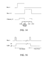
- FIG. 14 illustrates a timing set for the layout of FIG. 13 .
- FIG. 15 illustrates a handheld device together with an optical wand.
- FIG. 16 illustrates even/odd frame addressing.
- FIG. 17 illustrates a front illuminated display
- FIG. 18 illustrates total internal reflections.
- FIG. 19 illustrates a small amount of diffraction of the propagating light.
- FIG. 20 illustrates significant diffraction as a result of a plastic pen.
- FIG. 21 illustrates a shadow of a pointing device and a shadow with illuminated region of a pointing device.
- FIG. 22 illustrates a modified black matrix arrangement
- FIG. 23 illustrates a light reflecting structure
- FIG. 24 illustrates a pen
- FIG. 25 illustrates a light guide and finger.
- FIG. 26 illustrates a display with multiple sensor densities and optical elements.
- FIG. 27 illustrates a display with memory maintaining material.
- FIG. 28 illustrates another pen.
- FIG. 29 illustrates another pen.
- FIG. 30 illustrates another pen.
- FIG. 31 illustrates another pen.
- FIG. 32 illustrates another light guide.
- FIG. 33 illustrates an image acquisition and processing technique.
- a liquid crystal display (LCD) 50 (indicated by a bracket) comprises generally, a backlight 52 and a light valve 54 (indicated by a bracket). Since liquid crystals do not emit light, most LCD panels are backlit with fluorescent tubes or arrays of light-emitting diodes (LEDs) that are built into the sides or back of the panel. To disperse the light and obtain a more uniform intensity over the surface of the display, light from the backlight 52 typically passes through a diffuser 56 before impinging on the light valve 54 .
- LEDs light-emitting diodes
- the transmittance of light from the backlight 52 to the eye of a viewer 58 , observing an image displayed on the front of the panel, is controlled by the light valve 54 .
- the light valve 54 normally includes a pair of polarizers 60 and 62 separated by a layer of liquid crystals 64 contained in a cell gap between glass or plastic plates, and the polarizers.
- Light from the backlight 52 impinging on the first polarizer 62 comprises electromagnetic waves vibrating in a plurality of planes. Only that portion of the light vibrating in the plane of the optical axis of the polarizer passes through the polarizer.
- the optical axes of the first 62 and second 60 polarizer are typically arranged at an angle so that light passing through the first polarizer would normally be blocked from passing through the second polarizer in the series.
- the orientation of the translucent crystals in the layer of liquid crystals 64 can be locally controlled to either “twist” the vibratory plane of the light into alignment with the optical axes of the polarizer, permitting light to pass through the light valve creating a bright picture element or pixel, or out of alignment with the optical axis of one of the polarizers, attenuating the light and creating a darker area of the screen or pixel.
- first glass substrate 61 and a second glass substrate 63 form the walls of the cell gap and are buffed to produce microscopic grooves to physically align the molecules of liquid crystal 64 immediately adjacent to the walls.
- Molecular forces cause adjacent liquid crystal molecules to attempt to align with their neighbors with the result that the orientation of the molecules in the column of molecules spanning the cell gap twist over the length of the column.
- the plane of vibration of light transiting the column of molecules will be “twisted” from the optical axis of the first polarizer 62 to a plane determined by the orientation of the liquid crystals at the opposite wall of the cell gap.
- a voltage typically controlled by a thin film transistor, is applied to an electrode in an array of transparent electrodes deposited on the walls of the cell gap.
- the liquid crystal molecules adjacent to the electrode are attracted by the field produced by the voltage and rotate to align with the field.
- the column of crystals is “untwisted,” and the optical axes of the crystals adjacent to the cell wall are rotated progressively out of alignment with the optical axis of the corresponding polarizer progressively reducing the local transmittance of the light valve 54 and attenuating the luminance of the corresponding pixel.
- a normally white twisted nematic device there are generally two modes of operation, one without a voltage applied to the molecules and one with a voltage applied to the molecules.
- a voltage applied e.g., driven mode
- the molecules rotate their polarization axis which results in inhibiting the passage of light to the viewer.
- the polarization axis is not rotated so that the passage of light is not inhibited to the viewer.
- the polarizers and buffing of the light valve can be arranged to produce a “normally black” LCD having pixels that are dark (light is blocked) when the electrodes are not energized and light when the electrodes are energized.
- Color LCD displays are created by varying the intensity of transmitted light for each of a plurality of primary color (typically, red, green, and blue) sub-pixels that make up a displayed pixel.
- a twisted nematic device was described with respect to a twisted nematic device.
- this description is only an example and other devices may likewise be used, including but not limited to, multi-domain vertical alignment, patterned vertical alignment, in-plane switching, and super-twisted nematic type LCDs.
- other devices such as for example, plasma displays, organic displays, active matrix organic light emitting display, electroluminescent displays, liquid crystal on silicon displays, reflective liquid crystal devices may likewise be used.
- the light emitting portion of the display, or portion of the display that permits the display of selected portions of light may be considered to selectively cause the pixels to provide light.
- the inner surface of the second glass substrate 63 is normally coated with a continuous electrode while the first glass substrate 61 is patterned into individual pixel electrodes.
- the continuous electrode may be constructed using a transparent electrode, such as indium tin oxide.
- the first glass substrate 61 may include thin film transistors (TFTs) which act as individual switches for each pixel electrode (or group of pixel electrodes) corresponding to a pixel (or group of pixels).
- TFTs thin film transistors
- the TFTs are addressed by a set of multiplexed electrodes running along the gaps between the pixel electrodes.
- the pixel electrodes may be on a different layer from the TFTs.
- a pixel is addressed by applying voltage (or current) to a selected line, which switches the TFT on and allows charge from the data line to flow onto the rear pixel electrodes.
- the combination of voltages between the front electrode and the pixel electrodes sets up a voltage across the pixels and turns the respective pixels on.
- the thin-film transistors are typically constructed from amorphous silicon, while other types of switching devices may likewise be used, such as for example, metal-insulator-metal diode and polysilicon thin-film transistors.
- the TFT array and pixel electrodes may alternatively be on the top of the liquid crystal material. Also, the continuous electrode may be patterned or portions selectively selected, as desired. Also the light sensitive elements may likewise be located on the top, or otherwise above, of the liquid crystal material, if desired.
- the active matrix layer may include a set of data lines and a set of select lines. Normally one data line is included for each column of pixels across the display and one select line is included for each row of pixels down the display, thereby creating an array of conductive lines.
- a set of voltages are imposed on the respective data lines 204 which imposes a voltage on the sources 202 of latching transistors 200 .
- the selection of a respective select line 210 interconnected to the gates 212 of the respective latching transistors 200 , permits the voltage imposed on the sources 202 to be passed to the drain 214 of the latching transistors 200 .
- the drains 214 of the latching transistors 200 are electrically connected to respective pixel electrodes and are capacitively coupled to a respective common line 221 through a respective Cst capacitor 218 .
- a respective capacitance exists between the pixel electrodes enclosing the liquid crystal material, noted as capacitances Clc 222 (between the pixel electrodes and the common electrode on the color plate).
- the common line 221 provides a voltage reference.
- the voltage data (representative of the image to be displayed) is loaded into the data lines for a row of latching transistors 200 and imposing a voltage on the select line 210 latches that data into the holding capacitors and hence the pixel electrodes.
- the display may be operated based upon current levels.
- the pixel electrodes 230 are generally grouped into a “single” effective pixel so that a corresponding set of pixel electrodes 230 may be associated with respective color filters (e.g., red, green, blue).
- the latching transistors 200 interconnect the respective pixel electrodes 230 with the data lines and the select line.
- the pixel electrodes 230 may be interconnected to the common line 221 by the capacitors Cst 218 .
- the pixels may include any desirable shape, any number of sub-pixels, and any set of color filters.
- the active matrix layer may be constructed using an amorphous silicon thin-film transistor fabrication process.
- the steps may include gate metal deposition ( FIG. 4A ), a photolithography/etch ( FIG. 4B ), a gate insulator and amorphous silicon deposition ( FIG. 4C ), a photolithography/etch ( FIG. 4D ), a source/drain metal deposition (FIG. 4 E), a photolithography/etch ( FIG. 4F ), an ITO deposition ( FIG. 4G ), and a photolithography/etch ( FIG. 4H ).
- Other processes may likewise be used, as desired.
- the present inventors considered different potential architectural touch panel schemes to incorporate additional optical layers between the polarizer on the front of the liquid crystal display and the front of the display.
- additional layers include, for example, glass plates, wire grids, transparent electrodes, plastic plates, spacers, and other materials.
- the present inventors considered the additional layers with different optical characteristics, such as for example, birefringence, non-birefringence, narrow range of wavelengths, wide range of wavelengths, etc.
- the present inventors determined that an optimized touch screen is merely a tradeoff between different undesirable properties. Accordingly, the design of an optimized touch screen is an ultimately unsolvable task. In contrast to designing an improved touch screen, the present inventors came to the realization that modification of the structure of the active matrix liquid crystal device itself could provide an improved touch screen capability without all of the attendant drawbacks to the touch screen configuration located on the front of the display.
- a black matrix 240 is overlying the latching transistors so that significant ambient light does not strike the transistors.
- Color filters 242 may be located above the pixel electrodes. Ambient light striking the latching transistors results in draining the charge imposed on the pixel electrodes through the transistor. The discharge of the charge imposed on the pixel electrodes results in a decrease in the operational characteristics of the display, frequently to the extent that the display is rendered effectively inoperative.
- amorphous silicon transistors are sensitive to light incident thereon
- the present inventors determined that such transistors within the active matrix layer may be used as a basis upon which to detect the existence of or non-existence of ambient light incident thereon (e.g., relative values thereto).
- a modified active matrix layer may include a photo-sensitive structure or elements.
- the preferred photo-sensitive structure includes a photo-sensitive thin film transistor (photo TFT) interconnected to a readout thin film transistor (readout TFT).
- a capacitor Cst 2 may interconnect the common line to the transistors.
- a black matrix may be in an overlying relationship to the readout TFT.
- the black matrix is preferably an opaque material or otherwise the structure of the display selectively inhibiting the transmission of light to selective portions of the active matrix layer.
- the black matrix is completely overlying the amorphous silicon portion of the readout TFT, and at least partially overlying the amorphous silicon portion of the readout TFT.
- the black matrix is completely non-overlying the amorphous silicon portion of the photo TFT, and at least partially non-overlying the amorphous silicon portion of the photo TFT. Overlying does not necessarily denote direct contact between the layers, but is intended to denote in the general sense the stacked structure of materials.
- the black matrix is preferably fabricated on a layer other than the active plate, such as the color plate.
- the active plate is normally referred to as the plate supporting the thin-film transistors. The location of the black matrix on the color plate (or other non-active plate) results in limited additional processing or otherwise modification of the fabrication of the active matrix.
- the black matrix inhibits ambient light from impacting the amorphous silicon portion of the readout TFT to an extent greater than inhibiting ambient light from impacting the amorphous silicon portion of the photo TFT.
- a gate metal, or other light inhibiting material, may inhibit the photo-sensitive elements from the back light.
- the photo-sensitive areas are generally rectangular in shape, although other shapes may be used.
- the opening in the black matrix is preferably wider (or longer) than the corresponding channel area. In this manner the channel area and the opening in the black matrix are overlapping, with the opening extending in a first dimension (e.g., width) greater than the channel area and in a second dimension (e.g., length) less than the channel area.
- This alignment alleviates the need for precise registration of the layers while ensuring reasonable optical passage of light to the light sensitive element.
- Other relative sizes may likewise be used, as described.
- the common line may be set at a negative voltage potential, such as ⁇ 10 volts.
- a voltage is imposed on the select line which causes the voltage on the readout line to be coupled to the drain of the photo TFT and the drain of the readout TFT, which results in a voltage potential across Cst 2 .
- the voltage coupled to the drain of the photo TFT and the drain of the readout TFT is approximately ground (e.g., zero volts) with the non-inverting input of the operational amplifier connected to ground.
- the voltage imposed on the select line is removed so that the readout TFT will turn “off”.
- a voltage is imposed on the select line which causes the gate of the readout TFT to interconnect the imposed voltage on Cst 2 to the readout line. If the voltage imposed on the readout line as a result of activating the readout TFT is substantially unchanged, then the output of the operational amplifier will be substantially unchanged (e.g., zero). In this manner, the system is able to determine whether the light to the device has been inhibited, in which case the system will determine that the screen has been touched at the corresponding portion of the display with the photo TFT.
- the voltage imposed on the select line causes the voltage on the respective drain of the photo TFT and the drain of the readout TFT to be coupled to the respective readout line, which results in resetting the voltage potential across Cst 2 .
- the voltage coupled to the drain of the photo TFT and the drain of the readout TFT is approximately ground (e.g., zero volts) with the non-inverting input of the operational amplifier connected to ground.
- the voltage imposed on the select line is removed so that the readout TFT will turn “off”. In this manner, the act of reading the voltage simultaneously acts to reset the voltage potential for the next cycle.
- a voltage is imposed on the select line which causes the gate of the readout TFT to interconnect the imposed voltage to the readout line. If the voltage imposed on the readout line as a result of activating the readout TFT is substantially changed or otherwise results in an injection of current, then the output of the operational amplifier will be substantially non-zero. The output voltage of the operational amplifier is proportional or otherwise associated with the charge on the capacitor Cst 2 . In this manner, the system is able to determine whether the light to the device has been uninhibited, in which case the system will determine that the screen has not been touched at the corresponding portion of the display with the photo TFT.
- a layout of the active matrix layer may include the photo TFT, the capacitor Cst 2 , and the readout TFT in a region between the pixel electrodes.
- Light sensitive elements are preferably included at selected intervals within the active matrix layer.
- the device may include touch panel sensitivity without the need for additional touch panel layers attached to the front of the display.
- the additional photo TFT, readout TFT, and capacitor may be fabricated together with the remainder of the active matrix layer, without the need for specialized processing.
- the complexity of the fabrication process is only slightly increased so that the resulting manufacturing yield will remain substantially unchanged. It is to be understood that other light sensitive elements may likewise be used.
- other light sensitive electrical architectures may likewise be used.
- Line 300 illustrates a dark ambient environment with the gate connected to the source of the photo TFT. It will be noted that the leakage currents are low and relatively stable over a range of voltages.
- Line 302 illustrates a dark ambient environment with a floating gate of the photo TFT. It will be noted that the leakage currents are generally low and relatively unstable over a range of voltages (significant slope).
- Line 304 illustrates a low ambient environment with the gate connected to the source of the photo TFT. It will be noted that the leakage currents are three orders of magnitude higher than the corresponding dark ambient conditions and relatively stable over a range of voltages.
- Line 306 illustrates a low ambient environment with a floating gate of the photo TFT. It will be noted that the leakage currents are generally three orders of magnitude higher and relatively unstable over a range of voltages (significant slope).
- Line 308 illustrates a high ambient environment with the gate connected to the source of the photo TFT. It will be noted that the leakage currents are 4.5 orders of magnitude higher than the corresponding dark ambient conditions and relatively stable over a range of voltages.
- Line 310 illustrates a high ambient environment with a floating gate of the photo TFT. It will be noted that the leakage currents are generally 4.5 orders of magnitude higher and relatively unstable over a range of voltages (significant slope).
- the system may readily process the data in a confident manner, especially with the gate connected to the source.
- the architecture preferably permits the leakage currents to be within one order of magnitude over the central 50%, more preferably over the central 75%, of the voltage range used for displaying images.
- the photo TFT will tend to completely discharge the Cst 2 capacitor to the common voltage, perhaps with an offset voltage because of the photo TFT. In this manner, all of the photo TFTs across the display will tend to discharge to the same voltage level. Those regions with reduced ambient lighting conditions or otherwise where the user blocks ambient light from reaching the display, the Cst 2 capacitor will not fully discharge, as illustrated by the downward spike in the graph.
- the downward spike in the graph provides location information related to the region of the display that has been touched.
- the photo TFT will tend to partially discharge the Cst 2 capacitor to the common voltage. In this manner, all of the photo TFTs across the display will tend to discharge to some intermediate voltage levels. Those regions with further reduced ambient lighting conditions or otherwise where the user blocks ambient light from reaching the display, the Cst 2 capacitor will discharge to a significantly less extent, as illustrated by the downward spike in the graph.
- the downward spike in the graph provides location information related to the region of the display that has been touched. As shown in FIGS. 9 and 10 , the region or regions where the user inhibits light from reaching the display may be determined as localized minimums. In other embodiments, depending on the circuit topology, the location(s) where the user inhibits light from reaching the display may be determined as localized maximums or otherwise some measure from the additional components.
- the value of the capacitor Cst 2 may be selected such that it is suitable for high ambient lighting conditions or low ambient lighting conditions.
- a smaller capacitance may be selected so that the device is more sensitive to changes in light.
- a larger capacitance may be selected so that the device is less sensitive to changes in light.
- the dimensions of the phototransistor may be selected to change the photo-leakage current.
- one set of light sensitive elements e.g., the photo TFT and the capacitance
- another set of light sensitive elements e.g., the photo TFT and the capacitance
- the data from light sensitive elements for low ambient conditions and the data from light sensitive elements for high ambient conditions are separately processed, and the suitable set of data is selected.
- the same display device may be used for high and low ambient lighting conditions.
- multiple levels of sensitivity may be provided. It is to be understood that a single architecture may be provided with a wide range of sensitivity from low to high ambient lighting conditions.
- any suitable alternative architecture may be used for sensing the decrease and/or increase in ambient light.
- Another structure that may be included is selecting the value of the capacitance so that under normal ambient lighting conditions the charge on the capacitor only partially discharges.
- an optical pointing device such as a light wand or laser pointer, might be used to point at the display to further discharge particular regions of the display.
- the region of the display that the optical pointing device remains pointed at may be detected as local maximums (or otherwise).
- those regions of the display where light is inhibited will appear as local minimums (or otherwise). This provides the capability of detecting not only the absence of light (e.g., touching the panel) but likewise those regions of the display that have increased light incident thereon. Referring to FIG.
- a graph illustrates local minimums (upward peaks) from added light and local maximums (downward peaks) from a lack of light.
- one set of light sensitive elements e.g., the photo TFT and the capacitance
- the display may be optimized for ambient lighting conditions to detect the absence of light while another set of light sensitive elements (e.g., the photo TFT and the capacitance) within the display may be optimized for ambient lighting conditions to detect the additional light imposed thereon.
- a switch associated with the display may be provided to select among a plurality of different sets of light sensitive elements. For example, one of the switches may select between low, medium, and high ambient lighting conditions. For example, another switch may select between a touch sensitive operation (absence of light) and an optical pointing device (addition of light). In addition, the optical pointing device may communicate to the display, such as through a wire or wireless connection, to automatically change to the optical sensing mode.
- a light sensor external photo-sensor to the light sensitive elements in the active layer
- one or more of the light sensitive elements may be used to sense the ambient lighting conditions to select among different sets of light sensitive elements. Also the sensor and/or one or more light sensitive elements may be used to select, (1) to sense the absence of light, (2) select to sense the addition of light, and/or (3) adjust the sensing levels of the electronics.
- the corresponding color filters for (e.g., above) some or all of the light sensitive elements may be omitted or replaced by a clear (or substantially clear) material. In this manner the light reaching some of the light sensitive elements will not be filtered by a color filter. This permits those light sensitive elements to sense a greater dynamic range or a different part of the dynamic range than those receiving filtered light.
- the teachings herein are likewise applicable to transmissive active matrix liquid crystal devices, reflective active matrix liquid crystal devices, transflective active matrix liquid crystal devices, etc.
- the light sensitive elements may likewise be provided within a passive liquid crystal display.
- the sensing devices may be, for example, photo resistors and photo diodes.
- light sensitive elements may be provided between the rear polarizing element and the active matrix layer.
- the light sensitive elements are preferably fabricated on the polarizer, or otherwise a film attached to the polarizer.
- the light sensitive elements may be provided on a thin glass plate between the polarizer and the liquid crystal material.
- the black matrix or otherwise light inhibiting material is preferably arranged so as to inhibit ambient light from striking the readout TFT while free from inhibiting light from striking the photo TFT.
- a light blocking material is provided between the photo TFT and/or the readout TFT and the backlight, such as gate metal, if provided, to inhibit the light from the backlight from reaching the photo TFT and/or the readout TFT.
- light sensitive elements may be provided between the front polarizing element and the liquid crystal material.
- the light sensitive elements are preferably fabricated on the polarizer, or otherwise a film attached to the polarizer.
- the light sensitive elements may be provided on a thin glass plate between the polarizer and the liquid crystal material.
- the light sensitive elements may likewise be fabricated within the front electrode layer by patterning the front electrode layer and including suitable fabrication techniques.
- a black matrix or otherwise light inhibiting material is preferably arranged so as to inhibit ambient light from striking the readout TFT while free from inhibiting light from striking the photo TFT.
- a light blocking material is provided between the photo TFT and/or the readout TFT and the backlight, if provided, to inhibit the light from the backlight from reaching the photo TFT and/or the readout TFT.
- light sensitive elements may be provided between the front of the display and the rear of the display, normally fabricated on one of the layers therein or fabricated on a separate layer provided within the stack of layers within the display.
- the light sensitive elements are preferably provided between the front of the display and the backlight material.
- the position of the light sensitive elements are preferably between (or at least partially) the pixel electrodes, when viewed from a plan view of the display. This may be particularly useful for reflective displays where the pixel electrodes are opaque. In addition for reflective displays, any reflective conductive electrodes should be arranged so that they do not significantly inhibit light from reaching the light sensitive elements.
- the light sensitive elements are preferably fabricated on one or more of the layers, or otherwise a plate attached to one or more of the layers.
- a black matrix or otherwise light inhibiting material is preferably arranged so as to inhibit ambient light from striking the readout TFT while free from inhibiting light from striking the photo TFT.
- a light blocking material is provided between the photo TFT and/or the readout TFT and the backlight, if provided, to inhibit the light from the backlight from reaching the photo TFT and/or the readout TFT.
- the integrated light sensitive elements within the display stack may be used as a measure of the ambient lighting conditions to control the intensity of the backlight without the need for an additional external photo-sensor.
- One light sensitive element may be used, or a plurality of light sensitive element may be used together with additional processing, such as averaging.
- the readout line may be included in a periodic manner within the display sufficient to generally identify the location of the “touch”. For example the readout line may be periodically added at each 30 th column. Spacing the readout lines at a significant number of pixels apart results in a display that nearly maintains its previous brightness because most of the pixel electrodes have an unchanged size. However, after considerable testing it was determined that such periodic spacing results in a noticeable non-uniform gray scale because of differences in the size of the active region of the pixel electrodes.
- One potential resolution of the non-uniform gray scale is to modify the frame data in a manner consistent with the non-uniformity, such as increasing the gray level of the pixel electrodes with a reduced size or otherwise reducing the gray levels of the non-reduced size pixel electrodes, or a combination thereof. While a potential resolution, this requires additional data processing which increases the computational complexity of the system.
- a more desirable resolution of the non-uniform gray scale is to modify the display to include a readout line at every third pixel, or otherwise in a manner consistent with the pixel electrode pattern of the display (red pixel, green pixel, blue pixel).
- a readout line is included at least every 12 th pixel (36 pixel electrodes of a red, blue, green arrangement), more preferably at least every 9 th pixel (27 pixel electrodes of a red, blue, green arrangement), even more preferably at least every 6 th pixel (18 pixel electrodes of a red, blue, green arrangement or 24 pixel electrodes of a red, blue, green arrangement), and most preferably at least every 3 rd pixel (3 pixel electrodes of a red, blue, green arrangement).
- the readout lines are preferably included for at least a pattern of four times the spacing between readout lines (e.g., 12 th pixel times 4 equals 48 pixels, 9 th pixel times 4 equals 36 pixels). More preferably the pattern of readout lines is included over a majority of the display.
- the resulting display may include more readout lines than are necessary to accurately determine the location of the “touch”.
- a selection of the readout lines may be free from interconnection or otherwise not operationally interconnected with readout electronics.
- the readout lines not operationally interconnected with readout electronics may likewise be free from an associated light sensitive element.
- additional non-operational readout lines may be included within the display to provide a gray scale display with increased uniformity.
- one or more of the non-operational readout lines may be replaced with spaces.
- the gray scale display may include increased uniformity, albeit with additional spaces within the pixel electrode matrix.
- the present inventors considered the selection of potential pixel electrodes and came to the realization that the electrode corresponding to “blue” light does not contribute to the overall white transmission to the extent that the “green” or “red” electrodes. Accordingly, the system may be designed in such a manner that the light sensitive elements are associated with the “blue” electrodes to an extent greater than their association with the “green” or “red” electrodes. In this manner, the “blue” pixel electrodes may be decreased in size to accommodate the light sensitive elements while the white transmission remains substantially unchanged. Experiments have shown that reducing the size of the “blue” electrodes to approximately 85% of their original size, with the “green” and “red” electrodes remaining unchanged, results in a reduction in the white transmission by only about 3 percent.
- the reduction of pixel apertures results in a reduction of brightness normally by at least 5 percent and possibly as much as 15 percent depending on the resolution and layout design rules employed.
- the manufacturing yield is decreased because the readout line has a tendency to short to its neighboring data line if the processing characteristics are not accurately controlled.
- the data line and readout line may be approximately 6-10 microns apart along a majority of their length.
- the present inventors came to the realization that the readout of the photo-sensitive circuit and the writing of data to the pixels may be combined on the same bus line, or otherwise a set of lines that are electrically interconnected to one another.
- a switch 418 may select between providing new data 420 to the selected pixels and reading data 414 from the selected pixels. With the switch 418 set to interconnect the new data 420 with the selected pixels, the data from a frame buffer or otherwise the video data stream may be provided to the pixels associated with one of the select lines.
- Multiple readout circuits may be used, or one or more multiplexed readout circuits may be used.
- the new data 420 provided on data line 400 may be 4.5 volts which is latched to the pixel electrode 402 and the photo TFT 404 by imposing a suitable voltage on the select line 406 . In this manner, the data voltage is latched to both the pixel electrode and a corresponding photo-sensitive circuit.
- the display is illuminated in a traditional manner and the voltage imposed on the photo TFT 404 may be modified in accordance with the light incident on the photo-sensitive circuit, as previously described.
- the photo TFT 404 is normally a N-type transistor which is reverse biased by setting the voltage on the common line 408 to a voltage lower than an anticipated voltage on the photo TFT 404 , such as ⁇ 10 or ⁇ 15 volts.
- the data for the current frame may be stored in a frame buffer for later usage. Prior to writing the data for another frame, such as the next frame, the data (e.g., voltage) on the readout TFT 410 is read out.
- the switch 418 changes between the new data 420 to the readout line 414 interconnected to the charge readout amplifier 412 .
- the select line 406 is again selected to couple the remaining voltage on the photo TFT 404 through the readout TFT 410 to the data line 400 .
- the coupled voltage (or current) to the data line 400 is provided as an input to the charge readout amplifier 412 which is compared against the corresponding data from the previous frame 422 , namely, the voltage originally imposed on the photo TFT 404 .
- the difference between the readout line 414 and the data from the previous frame 422 provides an output to the amplifier 412 .
- the output of the amplifier 412 is provided to the processor.
- the greater the drain of the photo TFT 404 normally as a result of sensing light, results in a greater output of the amplifier 412 . Referring to FIG. 14 , an exemplary timing for the writing and readout on the shared data line 400 is illustrated.
- the integrated optical touch panel is not expected to operate well to the touch of the finger because there will be an insufficient (or none) difference between the signals from the surrounding area and the touched area.
- a light pen or laser pointer may be used (e.g., light source), as previously described.
- the light source may be operably interconnected to the display such as by a wire or wireless communication link. With the light source operably interconnected to the display the intensity of the light source may be controlled, at least in part, by feedback from the photo-sensitive elements or otherwise the display, as illustrated in FIG. 15 . When the display determines that sufficient ambient light exists, such as ambient light exceeding a threshold value, the light source is turned “off”.
- touching the light source against the display results in the same effect as touching a finger against the display, namely, impeding ambient light from striking the display.
- the display determines that insufficient ambient light exists, such as ambient light failing to exceed a threshold value, the light source is turned “on”.
- touching or otherwise directing the light from the light source against the display results in a localized increase in the received light relative to the ambient light level.
- the display may be operated in dark ambient lighting conditions or by feedback from the display.
- the intensity of the light from the light source may be varied, such as step-wise, linearly, non-linearly, or continuously, depending upon the ambient lighting conditions.
- the light source may include its own ambient light detector so that feedback from the display is unnecessary and likewise communication between the light source and the display may be unnecessary.
- the present inventors considered this situation and determined that by providing light during different frames, such as odd frames or even frames, or odd fields or even fields, or every third frame, or during selected frames, a more defined differential signal between the frames indicates the “touch” location.
- the light may be turned on and off in some manner, such as blinking at a rate synchronized with the display line scanning or frames.
- An exemplary timing for an odd/even frame arrangement is shown in FIG. 16 .
- the illumination of some types of displays involves scanning the display in a row-by-row manner.
- the differential signal may be improved by modifying the timing of the light pulses in accordance with the timing of the gate pulse (e.g., scanning) for the respective pixel electrodes. For example, in a top-down scanning display the light pulse should be earlier when the light source is directed toward the top of the display as opposed to the bottom of the display.
- the synchronization may be based upon feedback from the display, if desired.
- the light source may blink at a rate synchronized with the display line scanning.
- the light source may use the same driver source as the image pixel electrodes.
- the use of sequential (or otherwise) frames may be subtracted from one another which results in significant difference between signal and ambient conditions.
- the light sensitive elements have a dynamic range greater than 2 decades, and more preferably a dynamic range greater than 4 decades. If desired, the system may use two sequential fields of scanning (all lines) subtracted from the next two fields of scanning (all lines) so that all the lines of the display are used.
- Another technique for effective operation of the display in dark or low level ambient conditions is using a pen or other device with a light reflecting surface that is proximate (touching or near touching) the display when interacting with the display.
- the light from the backlight transmitted through the panel is then reflected back into the photo-sensitive element and the readout signal will be greater at the touch location than the surrounding area.
- another type of reflective liquid crystal display typically used on handheld computing devices, involves incorporating a light guide in front of the liquid crystal material, which is normally a glass plate or clear plastic material.
- the light guide is constructed from an opaque material having an index of refraction between 1.4 and 1.6, more typically between 1.45 and 1.50, and sometimes of materials having an index of refraction of 1.46.
- the light guide may further include anti-glare and anti-reflection coatings.
- the light guide is frequently illuminated with a light source, frequently disposed to the side of the light guide.
- the light source may be any suitable device, such as for example, a cold cathode fluorescent lamp, an incandescent lamp, and a light emitting diode.
- a reflector may be included behind the lamp to reflect light that is emitted away from the light guide, and to re-direct the light into the light guide.
- the light propagating within the light guide bounces between the two surfaces by total internal reflections. The total internal reflections will occur for angles that are above the critical angle, measured relative to the normal to the surfaces, as illustrated in FIG. 18 .
- one suitable technique for the localized diffusion of light involves using a plastic pen to touch the front of the display.
- the internally reflected light coincident with the location that the pen touches the display will significantly diffuse and be directed toward the photo sensitive elements within the display.
- the plastic pen, or other object including the finger or the eraser of a pencil preferably has an index of refraction within 0.5, more preferably within 0.25, of the index of refraction of the light guide.
- the index of refraction of the light guide may be between 1.2 and 1.9, and more preferably between 1.4 and 1.6.
- the plastic pen preferably has sufficient reflectivity of light as opposed to being non-reflective material, such as for example, black felt.
- the present inventors were surprised to note that a white eraser a few millimeters away from the light guide results in a darkened region with generally consistent optical properties while a white eraser in contact with the light guide results in a darkened region with generally consistent optical properties together with a smaller illuminated region.
- the light sensitive elements are positioned toward the front of the display in relation to the liquid crystal material (or otherwise the light valve or electroluminescent material) so that a clearer image may be obtained. It is to be understood that any suitable pointing device may be used.
- the illuminated region has an illumination brighter in relation to the remainder of the darkened region.
- the illuminated region may be located by any suitable technique, such as for example, a center of gravity technique.
- the display screen will have a relatively light colored region, such as white or tan, which is used as a virtual button for operating software. Within this light colored region is typically textual information in relatively dark letters. In liquid crystal display technology the light colored region is indicative of light passing through the liquid crystal material. Accordingly, if a pointing instrument includes a generally reflective material the light passing through the display may be reflected back through the display. The light reflected back through the display may be sensed by the light sensitive elements.
- a relatively light colored region such as white or tan
- the light colored region is indicative of light passing through the liquid crystal material. Accordingly, if a pointing instrument includes a generally reflective material the light passing through the display may be reflected back through the display. The light reflected back through the display may be sensed by the light sensitive elements.
- the present inventors came to the realization that when users use a “touch panel” display, there is a likelihood that the pointing device (or finger) may “hover” at a location above the display. Normally, during this hovering the user is not actually selecting any portion of the display, but rather still deciding where to select. In this manner, the illuminated region is beneficial because it provides a technique for the determination between when the user is simply “hovering” and the user has actually touched (e.g., “touching”) the display.
- the sensitivity to hovering may be related to the light sensitive elements being primarily sensitive to collimated light which is inhibited by the finger or other element in proximity to the device because of the alignment of the opening in the black matrix to the pixel electrodes.
- the black matrix may include central material aligned with the respective pixel electrodes so that the light sensitive elements have an increased sensitivity to non-collimated light (or otherwise non-perpendicular or otherwise angled incident light), as illustrated in FIG. 22 .
- the openings may be considered a non-continuous opening or otherwise the spatial opening for a particular pixel is noncontinuous.
- Another potential technique for the determination between “hovering” and “touching” is to temporally model the “shadow” region (e.g., light impeded region of the display).
- the shadow e.g., light impeded region of the display.
- the end of the shadow will typically remain stationary for a period of time, which may be used as a basis, at least in part, of “touching”.
- the shadow will typically enlarge as the pointing device approaches the display and shrinks as the pointing device recedes from the display, where the general time between enlarging and receding may be used as a basis, at least in part, of “touching”.
- the shadow will typically enlarge as the pointing device approaches the display and maintain the same general size when the pointing device is touching the display, where the general time where the shadow maintains the same size may be used as a basis, at least in part, of “touching”.
- the shadow will typically darken as the pointing device approaches the display and maintain the same shade when the pointing device is touching the display, where the general time where the shadow maintains the same general shade may be used as a basis, at least in part, of “touching”.
- a light directing structure may be used.
- One such light directing structure is shown in FIG. 23 .
- the light directing structure is preferably included around a portion of the periphery of the display and may reflect ambient light across the frontal region of the display. The reflected light then reflects off the finger or other device thus increasing the light striking the light sensitive element when the finger or other device is spaced sufficiently apart from the display. The light reflecting off the finger or other device decreases when the finger or other device is near the display because of the angular reflections of light.
- the differences in the reflected light striking the display may be used, at least in part, to detect the touching of the display or otherwise inhibiting light to the display.
- the display portion of a handheld device has a refresh rate generally less than the refresh rate of the portion of the handwriting recognition portion of the display.
- the handheld portion of the display may use any recognition technique, such as Palm OS® based devices.
- the refresh rate of the display is typically generally 60 hertz while the refresh rate of the handwriting portion of the display is typically generally 100 hertz. Accordingly, the light-sensitive elements should be sampled at a sampling rate corresponding with the refresh rate of the respective portion of the display.
- the technique described with respect to FIG. 20 operates reasonably well in dark ambient lighting conditions, low ambient lighting conditions, regular ambient lighting conditions, and high ambient lighting conditions.
- the display is alleviated of a dependency on the ambient lighting conditions.
- the illumination point is more pronounced and thus easier to extract.
- the ambient light may be sufficiently high causing the detection of the pointing device to be difficult.
- shades of the ambient light may also interfere with the detection techniques.
- the present inventors considered improving the robustness of the detection techniques but came to the realization that with sufficient “noise” in the system the creation of such sufficiently robust techniques would be difficult.
- the present inventors came to the realization that by providing light to the light guide of a limited selection of wavelengths and selectively filtering the wavelengths of light within the display the difference between touched and un-touched may be increased.
- the light from the light source provided to the light guide is modified, or otherwise filtered, to provide a single color.
- the light source may provide light of a range of wavelengths, such as 600-700 nm, or 400-500 and 530-580, or 630.
- the light provided to the light guide has a range of wavelengths (in any significant amount) less than white light or otherwise the range of wavelengths of ambient light. Accordingly, with the light provided to the light guide having a limited color gamut (or reduced color spectrum) the touching of the pointing device on the display results in the limited color gamut light being locally directed toward the light-sensitive elements. With a limited color gamut light being directed toward the display as a result of touching the light guide (or otherwise touching the front of the display), a color filter may be included between the light guide and the light-sensitive elements to filter out at least a portion of the light not included within the limited color gamut.
- the color filter reduces the transmission of ambient light to an extent greater than the transmission of light from the light source or otherwise within the light guide.
- the ambient light may be considered as “white” light while the light guide has primarily “red” light therein.
- a typical transmission of a red color filter for ambient white light may be around 20%, while the same color filter will transmit about 85% of the red light.
- the transmission of ambient light through the color filter is less than 75% (greater than 25% attenuation) (or 60%, 50%, 40%, 30%) while the transmission of the respective light within the light guide is greater than 25% (less than 25% attenuation) (or 40%, 50%, 60%, 70%), so that in this manner there is sufficient attenuation of selected wavelengths of the ambient light with respect to the wavelengths of light within the light guide to increase the ability to accurately detect the touching.
- the light source to the light guide may include a switch or otherwise automatic modification to “white” light when operated in low ambient lighting conditions. In this manner, the display may be more effectively viewed at low ambient lighting conditions.
- the present inventors determined that if the light source providing light to the display was modulated in some fashion an improvement in signal detection may be achieved.
- a pointing device with a light source associated therewith may modulate the light source in accordance with the frame rate of the display. With a frame rate of 60 hertz the pointing device may for example modulate the light source at a rate of 30 hertz, 20 hertz, 10 hertz, etc. which results in additional light periodically being sensed by the light sensitive elements.
- the light source is modulated (“blinked”) at a rate synchronized with the display line scanning, and uses the same raw drivers as the image thin-film transistors.
- the resulting data may be processed in a variety of different ways.
- the signals from the light sensitive elements are used, as captured.
- the resulting improvement in signal to background ratio is related to the pulse length of the light relative to the frame time. This provides some additional improvement in signal detection between the light generated by the pointing device relative to the ambient light (which is constant in time).
- multiple frames are compared against one another to detect the presence and absence of the additional light resulting from the modulation.
- subsequent frames one without additional light and one with additional light
- the data from the light sensitive elements may be subtracted from one another.
- the improvement in signal to background ratio is related to the periodic absence of the additional light.
- this processing technique is especially suitable for low ambient lighting and high ambient lighting conditions.
- the dynamic range of the sensors is at least 4 decades, and two sequential frames with additional light and two sequential frames without additional light are used so that all of the scanning lines are encompassed.
- a pressure based mechanism may be used.
- One pressure based mechanism may include pressure sensitive tape between a pair of layers of the display or between the display and a support for the display.
- Another pressure based mechanism may include an electrical or magnetic sensor operably connected to the display. In either case, the pressure based mechanism provides a signal to the display electronics indicating the sensing of pressure (e.g., touch) or alternatively the absence of pressure (e.g., non-touch).
- an elongate light emitting device includes an infra-red light emitting diode that periodically or continuously emits an infra-red beam.
- the infra-red beam is transmitted from the light emitting device and reflects off the display.
- the reflected infra-red beam will not strike the light pen.
- the reflected infra-red beam will strike the light pen and is sensed by an infra-red sensor within the light pen.
- Infra-red light is preferred, while any suitable wavelength may be used that the light sensitive elements of the display are generally insensitive to.
- the visible light emitting diode When the infra-red sensor senses the reflected infra-red light the visible light emitting diode is turned on to illuminate the pixel.
- the visible light emitting diode preferably provides a wavelength that the light sensitive elements of the display are sensitive to. After a predetermined duration or otherwise while the infra-red light is not being sensed by the infra-red sensor the visible light emitting diode is turned off. In this manner, battery power within the light pen is conserved.
- the edge or shape of the visible light from the visible light emitting diode may be used to determine the spacing between the light pen and the display.
- the beam from the visible light emitting diode may be varied based upon the signal sensed by the infra-red sensor.
- the present inventors Upon reconsidering the display with a light guide, as illustrated in FIG. 17 , the present inventors realized that those portions of the light guide that are in contact with the high portion of the user's fingerprints will tend to diffuse and scatter light toward the light sensitive elements, as illustrated in FIG. 25 . Those portions of the light guide that are not in contact with the high portion of the user's fingerprints (i.e., valleys) will not tend to diffuse and scatter light toward the light sensitive elements. Depending on the thickness of the light guide and liquid crystal material together with the density of the light sensitive elements, the details observable in the fingerprint will vary. To increase the ability to detect the fingerprint, the display may be designed with multiple densities of light sensitive elements.
- the density of the light sensitive elements may be increased such as including a light sensitive element at every sub-pixel.
- the display includes multiple densities of light sensitive elements.
- the display may likewise be used for sensing other items, such as for example, bar codes.
- a separate sensor structure may be included within the display.
- the sensor structure may include a lens between the light guide and the light sensitive elements.
- the lens may be any suitable lens structure, such as for example, a small focus lens or a SELFOC lens (variable index of refraction fiber optics).
- the color filters in the fingerprint sensing region may be omitted, if desired.
- the display may include two (or more) different densities of light sensitive elements across the display.
- the light guide and lens may be omitted and a high density of light sensitive elements included for fingerprint sensing. It is to be understood that other items may likewise be sensed with the high density light sensitive elements.
- the light sensitive elements will tend to observe very high ambient lighting conditions when the finger is not present rendering their ability to detect high contrast images difficult.
- a color filter may be provided in an overlying relationship to the light sensitive elements.
- the light source may be selected in relation to the color filter.
- a blue filter may be used together with a blue light source.
- the illumination may be modulated and synchronized with the sensors.
- the light source may be illuminated with relatively short pulses together with the triggering of the sensing by the light sensitive elements.
- the light is pulsed in relation to the frame rate it is preferably pulsed at half the frame rate. In this manner the light pulses will be ensured to be sensed during different frames.
- a light inhibiting material may closely surround the region where the finger is located to reduce stray ambient light, thus increasing contrast.
- Sweat is primarily water with an index of refraction of approximately 1.3.
- Typical glass has an index of refraction of approximately 1.5 which is sufficiently different than 1.3, and accordingly sweat will not significantly negatively impact image sensing.
- oils have an index of refraction of approximately 1.44 to 1.47 which is considerably closer to 1.5, and accordingly oil will tend to significantly impact image sensing.
- the glass may be replaced with glass having a higher index of refraction or glass coated with a material having a higher index of refraction, such as for example, 1.55 or more.
- the display may include a signature portion that includes a memory maintaining material.
- the memory maintaining material may sense the writing of the signature, such as by pressure exerted thereon or light sensitive material.
- the memory material may be a pair of flexible layers with fluid there between that is displaced while writing the signature. After writing the name the user may press a button or otherwise touch another portion of the display indicating that the signature is completed.
- the display may sense the signature by a sufficient change in the optical properties of the memory maintaining material. The display may then capture an image of the signature.
- the image of the signature may come from ambient light passing through the memory maintaining material or otherwise from light reflected off the memory maintaining material, especially when the display is in transmissive (“white”) mode.
- the signature may be cleared in any manner, such as electrical erasure or physical erasure by any suitable mechanism. In this manner, the temporal limitations of writing a signature are reduced.
- the display may include a signature mode that captures the user's signature over several frames.
- the signature may be captured on a predetermined region of the display or otherwise any portion of the display.
- the system detects the decrease in ambient light over a series of frames as the signature is written. In this manner the “path” of the signature may be determined and thereafter used in any suitable manner.
- the pen may include a movable optical path (e.g., a fiber optic bundle) with respect to the pen that extends and retracts based upon pressure exerted on the display.
- a light emitting diode provides a beam of light that is channeled through the optical path.
- the light sensitive elements may detect the intensity of the transmitted light and determine the pressure that is being exerted against the display by the user. This capability is particularly useful for pressure sensitive applications, such as Photoshop by Adobe.
- a cylindrical tubular tip portion is movable with respect to the pen that extends and retracts based upon pressure exerted on the display.
- a lens Within the cylindrical tubular tip portion is a lens.
- the lens focuses the light emitted from a light emitting diode, which preferably is maintained stationary with respect to the pen and/or moves with respect to the cylindrical tubular tip portion.
- the light emitting diode may be connected to the tip portion of the pen.
- light may be more focused on the display (light sensitive elements) than when the cylindrical tubular tip portion is in an extended state.
- the lens may be modified so that it operates in a reversed manner.
- the focus of the beam may be detected in any suitable manner by the light sensitive elements (e.g., size and/or intensity) to determine the pressure that is being exerted against the display by the user.
- a cylindrical tubular tip portion or optical light guide is movable with respect to the pen that extends and retracts based upon pressure exerted on the display.
- the variable resistive element changes.
- the variable resistive element is interconnected to a light emitting diode which changes intensity based upon the change in the variable resistance.
- the intensity of light sensed by the light sensitive elements, or otherwise the change in intensity sensed by the light sensitive elements, may be used to determine the pressure that is being exerted against the display by the user.
- An optional lens focuses a beam from a light emitting diode.
- a larger spot size and/or intensity is sensed by the light sensitive elements with respect to when the pen is closer to the display.
- the intensity of the light and/or the size of the spot sensed by the light sensitive elements or otherwise the change in intensity and/or size may be used to determine the pressure that is being exerted against the display by the user.
- a polarizer may be included on the lower surface of the light guide.
- other polarizers may be included on the front and rear surfaces of the liquid crystal display.
- the polarizer on the lower surface of the light guide preferably matches ( ⁇ 5 degrees, ⁇ 2 degrees) the orientation of the polarizer on the front surface of the liquid crystal display.
- the polarizers may include anti-reflection coatings if desired. With the top two polarizers being included together with proper alignment between them more of the light from the pen will tend to pass through to the liquid crystal display.
- an exemplary image processing technique is illustrated for processing the data from the display to determine the location of the touch.
- the display is initially calibrated by a calibration image module.
- a calibration image module For calibration, an image is obtained with the display covered by a black cloth or otherwise blocked from receiving ambient light.
- the black reference image may be referred to as I 0 .
- an image may be obtained under normal uniform (e.g., without significant shadows or light spots) ambient lighting conditions and referred to as I 1 .
- a comparison between I 0 and I 1 may be performed to calibrate the display.
- the image is initially captured by a capture image module.
- a 60 ⁇ 60 sensor matrix may be captured.
- a set of consecutive frames may then be averaged by an average frame module in order to reduce the noise in the signal, such as for example four frames.
- An AGC module may perform an automatic gain control function in order to adjust for an offset in the value.
- Ie is the signal after equalization. “Is” is the sensor signal as captured or after averaging.
- I 0 is the stored sensor reading for the black reference image.
- I 1 is the stored sensor reading for the bright (e.g., ambient lighting conditions) reference image.
- the equalization module uses I 0 to adjust for the potential non-zero value at dark conditions. In particular, this adjustment is made by the calculation of Is ⁇ I 0 .
- the resulting comparison (e.g., division) of the captured signal versus the stored bright reference signals adjusts the level of the signal.
- the output of the equalization is a normalized signal with a range from 0 to 1 in the case that Is ⁇ I 1 . Ie may then be used to adjust the gain of the output of the average frame module or captured image value.
- the AGC module thus effectively corrects for dark level non-uniformity and for sensor gain non-uniformity.
- a smoothing module may be used to average proximate values together to compensate for non-uniformity in the characteristics of the display.
- a suitable filter is an averaging of the 8 adjacent pixels to a central pixel.
- the system provides relatively sharp edges from the signals which may be used directly.
- a preferred edge detection technique uses a 3 ⁇ 3 matrix, such as for example: ⁇ ( ⁇ 1 ⁇ 1 ⁇ 1) ( ⁇ 1 ⁇ 8 ⁇ 1) ( ⁇ 1 ⁇ 1 ⁇ 1) ⁇ .
- the effect of the edge detection module is to enhance or otherwise determine those regions of the image that indicate an edge.
- Other edge detection techniques may likewise be used, such as for example, a Sobel edge detection technique, a 1 st derivative technique, and a Robert's cross technique.
- a threshold module may be used to set all values below a predetermined threshold value to zero, or otherwise indicate that they are not edges or regions being touched. In the case that the system provides negative values the predetermined threshold value may be less than an absolute value. The use of threshold values assists in the discrimination between the end of the finger touching the display and the shade from the hand itself. If there are an insufficient number of pixels as a result of the threshold module that are non-thresholded then the system returns to the start.
- the system determines the largest region of non-thresholded values using a max location module. In this manner, smaller regions of a few values may be removed so that the predominant region of non-thresholded values may be determined.
- a center of gravity module may be used to determine the center of the maximum region from the max location module.
- An x-y coordinates module may be used to provide the x and y display coordinates and a plot cross module may be used to display a cross on the display at the x-y coordinates of the center of gravity.
- the cross module may provide data regarding the existence of the “touch” and its location to the system and return control back to the start.
- the display may become scratched or otherwise a foreign object will be stuck to the front of the display. In this case the display will tend to provide false readings that the scratch or foreign object is indicative of a touch.
- one or more bright reference images 11 may be obtained over a period of time. The set of one or more bright reference images 11 may be averaged if an insubstantial difference exists between the images. This reduces the likelihood that the display was touched during one or more of the image acquisitions. In the event that the images are substantially different then the images may be reacquired until an insubstantial difference exists.
Landscapes
- Engineering & Computer Science (AREA)
- Theoretical Computer Science (AREA)
- General Engineering & Computer Science (AREA)
- Physics & Mathematics (AREA)
- General Physics & Mathematics (AREA)
- Human Computer Interaction (AREA)
- Nonlinear Science (AREA)
- Crystallography & Structural Chemistry (AREA)
- Chemical & Material Sciences (AREA)
- Computer Hardware Design (AREA)
- Mathematical Physics (AREA)
- Optics & Photonics (AREA)
- Multimedia (AREA)
- Liquid Crystal (AREA)
- Control Of Indicators Other Than Cathode Ray Tubes (AREA)
- Position Input By Displaying (AREA)
- Devices For Indicating Variable Information By Combining Individual Elements (AREA)
Abstract
Description
Claims (17)
Priority Applications (1)
| Application Number | Priority Date | Filing Date | Title |
|---|---|---|---|
| US12/568,302 US9411470B2 (en) | 2002-02-20 | 2009-09-28 | Light sensitive display with multiple data set object detection |
Applications Claiming Priority (5)
| Application Number | Priority Date | Filing Date | Title |
|---|---|---|---|
| US35926302P | 2002-02-20 | 2002-02-20 | |
| US38304002P | 2002-05-23 | 2002-05-23 | |
| US10/371,413 US7280102B2 (en) | 2002-02-20 | 2003-02-20 | Light sensitive display |
| US11/901,649 US9134851B2 (en) | 2002-02-20 | 2007-09-18 | Light sensitive display |
| US12/568,302 US9411470B2 (en) | 2002-02-20 | 2009-09-28 | Light sensitive display with multiple data set object detection |
Related Parent Applications (1)
| Application Number | Title | Priority Date | Filing Date |
|---|---|---|---|
| US11/901,649 Continuation US9134851B2 (en) | 2002-02-20 | 2007-09-18 | Light sensitive display |
Publications (2)
| Publication Number | Publication Date |
|---|---|
| US20100013794A1 US20100013794A1 (en) | 2010-01-21 |
| US9411470B2 true US9411470B2 (en) | 2016-08-09 |
Family
ID=27766058
Family Applications (17)
| Application Number | Title | Priority Date | Filing Date |
|---|---|---|---|
| US10/217,798 Expired - Lifetime US7408598B2 (en) | 2002-02-20 | 2002-08-12 | Light sensitive display with selected interval of light sensitive elements |
| US10/307,106 Expired - Fee Related US6995743B2 (en) | 2002-02-20 | 2002-11-27 | Light sensitive display |
| US10/329,217 Expired - Lifetime US6947102B2 (en) | 2002-02-20 | 2002-12-23 | Light sensitive display which senses decreases in light |
| US10/371,413 Expired - Fee Related US7280102B2 (en) | 2002-02-20 | 2003-02-20 | Light sensitive display |
| US11/137,753 Abandoned US20050285985A1 (en) | 2002-02-20 | 2005-05-25 | Light sensitive display |
| US11/800,274 Abandoned US20070279346A1 (en) | 2002-02-20 | 2007-05-03 | Display with embedded image sensor |
| US11/901,649 Active 2029-04-05 US9134851B2 (en) | 2002-02-20 | 2007-09-18 | Light sensitive display |
| US11/977,995 Expired - Fee Related US7872641B2 (en) | 2002-02-20 | 2007-10-25 | Light sensitive display |
| US11/980,043 Abandoned US20080055507A1 (en) | 2002-02-20 | 2007-10-29 | Light sensitive display |
| US11/980,105 Abandoned US20080129913A1 (en) | 2002-02-20 | 2007-10-29 | Light sensitive display |
| US11/980,029 Abandoned US20080055499A1 (en) | 2002-02-20 | 2007-10-29 | Light sensitive display |
| US11/980,108 Abandoned US20080062343A1 (en) | 2002-02-20 | 2007-10-29 | Light sensitive display |
| US11/980,104 Abandoned US20080129909A1 (en) | 2002-02-20 | 2007-10-29 | Light sensitive display |
| US11/980,107 Abandoned US20080129914A1 (en) | 2002-02-20 | 2007-10-29 | Light sensitive display |
| US12/568,316 Abandoned US20100020044A1 (en) | 2002-02-20 | 2009-09-28 | Light sensitive display with switchable detection modes |
| US12/568,302 Expired - Fee Related US9411470B2 (en) | 2002-02-20 | 2009-09-28 | Light sensitive display with multiple data set object detection |
| US15/269,453 Expired - Fee Related US9971456B2 (en) | 2002-02-20 | 2016-09-19 | Light sensitive display with switchable detection modes for detecting a fingerprint |
Family Applications Before (15)
| Application Number | Title | Priority Date | Filing Date |
|---|---|---|---|
| US10/217,798 Expired - Lifetime US7408598B2 (en) | 2002-02-20 | 2002-08-12 | Light sensitive display with selected interval of light sensitive elements |
| US10/307,106 Expired - Fee Related US6995743B2 (en) | 2002-02-20 | 2002-11-27 | Light sensitive display |
| US10/329,217 Expired - Lifetime US6947102B2 (en) | 2002-02-20 | 2002-12-23 | Light sensitive display which senses decreases in light |
| US10/371,413 Expired - Fee Related US7280102B2 (en) | 2002-02-20 | 2003-02-20 | Light sensitive display |
| US11/137,753 Abandoned US20050285985A1 (en) | 2002-02-20 | 2005-05-25 | Light sensitive display |
| US11/800,274 Abandoned US20070279346A1 (en) | 2002-02-20 | 2007-05-03 | Display with embedded image sensor |
| US11/901,649 Active 2029-04-05 US9134851B2 (en) | 2002-02-20 | 2007-09-18 | Light sensitive display |
| US11/977,995 Expired - Fee Related US7872641B2 (en) | 2002-02-20 | 2007-10-25 | Light sensitive display |
| US11/980,043 Abandoned US20080055507A1 (en) | 2002-02-20 | 2007-10-29 | Light sensitive display |
| US11/980,105 Abandoned US20080129913A1 (en) | 2002-02-20 | 2007-10-29 | Light sensitive display |
| US11/980,029 Abandoned US20080055499A1 (en) | 2002-02-20 | 2007-10-29 | Light sensitive display |
| US11/980,108 Abandoned US20080062343A1 (en) | 2002-02-20 | 2007-10-29 | Light sensitive display |
| US11/980,104 Abandoned US20080129909A1 (en) | 2002-02-20 | 2007-10-29 | Light sensitive display |
| US11/980,107 Abandoned US20080129914A1 (en) | 2002-02-20 | 2007-10-29 | Light sensitive display |
| US12/568,316 Abandoned US20100020044A1 (en) | 2002-02-20 | 2009-09-28 | Light sensitive display with switchable detection modes |
Family Applications After (1)
| Application Number | Title | Priority Date | Filing Date |
|---|---|---|---|
| US15/269,453 Expired - Fee Related US9971456B2 (en) | 2002-02-20 | 2016-09-19 | Light sensitive display with switchable detection modes for detecting a fingerprint |
Country Status (3)
| Country | Link |
|---|---|
| US (17) | US7408598B2 (en) |
| AU (1) | AU2002336341A1 (en) |
| WO (1) | WO2003073159A1 (en) |
Families Citing this family (296)
| Publication number | Priority date | Publication date | Assignee | Title |
|---|---|---|---|---|
| US7663607B2 (en) | 2004-05-06 | 2010-02-16 | Apple Inc. | Multipoint touchscreen |
| US7009663B2 (en) * | 2003-12-17 | 2006-03-07 | Planar Systems, Inc. | Integrated optical light sensitive active matrix liquid crystal display |
| US7053967B2 (en) | 2002-05-23 | 2006-05-30 | Planar Systems, Inc. | Light sensitive display |
| US7408598B2 (en) | 2002-02-20 | 2008-08-05 | Planar Systems, Inc. | Light sensitive display with selected interval of light sensitive elements |
| US7023503B2 (en) * | 2002-02-20 | 2006-04-04 | Planar Systems, Inc. | Image sensor with photosensitive thin film transistors |
| WO2003075207A2 (en) * | 2002-03-01 | 2003-09-12 | Planar Systems, Inc. | Reflection resistant touch screens |
| TW546853B (en) * | 2002-05-01 | 2003-08-11 | Au Optronics Corp | Active type OLED and the fabrication method thereof |
| US20040017337A1 (en) * | 2002-07-24 | 2004-01-29 | Kinpo Electronics, Inc. | Adjustment device for light source of a panel |
| JP4093307B2 (en) * | 2002-10-01 | 2008-06-04 | 株式会社ニフコ | Silencer for fuel tank |
| US20060034492A1 (en) * | 2002-10-30 | 2006-02-16 | Roy Siegel | Hand recognition system |
| US20080084374A1 (en) * | 2003-02-20 | 2008-04-10 | Planar Systems, Inc. | Light sensitive display |
| US20080048995A1 (en) * | 2003-02-20 | 2008-02-28 | Planar Systems, Inc. | Light sensitive display |
| TWI363206B (en) * | 2003-02-28 | 2012-05-01 | Samsung Electronics Co Ltd | Liquid crystal display device |
| US20040207774A1 (en) * | 2003-04-17 | 2004-10-21 | Gothard David L. | Illumination apparatus for LCD/organic displays |
| US20040233174A1 (en) * | 2003-05-19 | 2004-11-25 | Robrecht Michael J. | Vibration sensing touch input device |
| US7432893B2 (en) * | 2003-06-14 | 2008-10-07 | Massachusetts Institute Of Technology | Input device based on frustrated total internal reflection |
| JP2005038729A (en) * | 2003-07-16 | 2005-02-10 | Sanyo Electric Co Ltd | EL display device |
| KR100973813B1 (en) * | 2003-08-06 | 2010-08-03 | 삼성전자주식회사 | Liquid Crystal Display and Image Signal Correction Method |
| US7145558B2 (en) * | 2003-09-03 | 2006-12-05 | Motorola, Inc. | Selective illumination of regions of an electronic display |
| US7649527B2 (en) * | 2003-09-08 | 2010-01-19 | Samsung Electronics Co., Ltd. | Image display system with light pen |
| US7432991B1 (en) * | 2003-10-01 | 2008-10-07 | Darwin Chang | Random access display monitor |
| US20070171157A1 (en) * | 2003-10-15 | 2007-07-26 | Samsung Electronics Co., Ltd | Display apparatus having photo sensor |
| KR100923025B1 (en) * | 2003-10-23 | 2009-10-22 | 삼성전자주식회사 | An optical sensing element, an array substrate and a liquid crystal display having the same |
| JP4521176B2 (en) * | 2003-10-31 | 2010-08-11 | 東芝モバイルディスプレイ株式会社 | Display device |
| KR100970958B1 (en) * | 2003-11-04 | 2010-07-20 | 삼성전자주식회사 | Liquid crystal display device having a touch screen function and manufacturing method thereof |
| US20050110777A1 (en) * | 2003-11-25 | 2005-05-26 | Geaghan Bernard O. | Light-emitting stylus and user input device using same |
| US7298367B2 (en) * | 2003-11-25 | 2007-11-20 | 3M Innovative Properties Company | Light emitting stylus and user input device using same |
| KR100983524B1 (en) * | 2003-12-01 | 2010-09-24 | 삼성전자주식회사 | Photosensitive panel, optical sensing device having same and driving method thereof |
| JP4265788B2 (en) * | 2003-12-05 | 2009-05-20 | シャープ株式会社 | Liquid crystal display |
| US20050134749A1 (en) * | 2003-12-19 | 2005-06-23 | Adiel Abileah | Reflection resistant display |
| CA2552650C (en) * | 2004-01-07 | 2014-09-30 | Identification International, Inc. | Low power fingerprint capture system, apparatus, and method |
| JP4261375B2 (en) * | 2004-01-15 | 2009-04-30 | 富士フイルム株式会社 | How to collect push shapes |
| US20050162380A1 (en) * | 2004-01-28 | 2005-07-28 | Jim Paikattu | Laser sensitive screen |
| US20050219229A1 (en) * | 2004-04-01 | 2005-10-06 | Sony Corporation | Image display device and method of driving image display device |
| US7773139B2 (en) | 2004-04-16 | 2010-08-10 | Apple Inc. | Image sensor with photosensitive thin film transistors |
| KR20050112878A (en) * | 2004-05-28 | 2005-12-01 | 삼성전자주식회사 | Electro phoretic indication display |
| JP4703206B2 (en) * | 2004-05-31 | 2011-06-15 | 東芝モバイルディスプレイ株式会社 | Display device with image capture function |
| US7586479B2 (en) | 2004-06-10 | 2009-09-08 | Samsung Electronics Co., Ltd. | Display device and driving method thereof |
| KR101054343B1 (en) * | 2004-06-10 | 2011-08-04 | 삼성전자주식회사 | Display device and driving method thereof |
| KR101018751B1 (en) * | 2004-09-24 | 2011-03-04 | 삼성전자주식회사 | Display device and driving method thereof |
| KR101160826B1 (en) * | 2004-11-08 | 2012-06-29 | 삼성전자주식회사 | Liquid crystal display including sensing element |
| US7671833B2 (en) * | 2004-11-22 | 2010-03-02 | Samsung Electronics Co., Ltd. | Touch sensible display device |
| KR20060065333A (en) * | 2004-12-10 | 2006-06-14 | 삼성전자주식회사 | Display panels and display devices with sensing elements |
| EP1831865A1 (en) * | 2004-12-21 | 2007-09-12 | Koninklijke Philips Electronics N.V. | Light source |
| DE102004063594A1 (en) * | 2004-12-30 | 2006-07-13 | BSH Bosch und Siemens Hausgeräte GmbH | Method for controlling the backlight of a display |
| JP2006276223A (en) * | 2005-03-28 | 2006-10-12 | Sony Corp | Display device and display method |
| US7570249B2 (en) * | 2005-03-30 | 2009-08-04 | Microsoft Corporation | Responding to change of state of control on device disposed on an interactive display surface |
| JP4338140B2 (en) * | 2005-05-12 | 2009-10-07 | 株式会社 日立ディスプレイズ | Touch panel integrated display device |
| KR100961072B1 (en) * | 2005-06-09 | 2010-06-01 | 엘지디스플레이 주식회사 | Liquid crystal display having an image sensing function, a manufacturing method thereof and an image sensing method using the same |
| JP2007003640A (en) * | 2005-06-22 | 2007-01-11 | Tohoku Pioneer Corp | Self-luminous panel |
| US20070012490A1 (en) * | 2005-06-28 | 2007-01-18 | Intel Corporation | Electromagnetic radiation input for user interface |
| KR20070008743A (en) * | 2005-07-12 | 2007-01-18 | 삼성전자주식회사 | Display panel and display device having same |
| KR101152132B1 (en) * | 2005-08-04 | 2012-06-15 | 삼성전자주식회사 | Liquid crystal display including sensing unit |
| KR101230303B1 (en) * | 2005-08-29 | 2013-02-06 | 삼성디스플레이 주식회사 | Touch sensible display device |
| KR20070033532A (en) * | 2005-09-21 | 2007-03-27 | 삼성전자주식회사 | Display device with touch sensing function, its driving device and sensing signal processing method |
| JP2007093849A (en) * | 2005-09-28 | 2007-04-12 | Sanyo Epson Imaging Devices Corp | Liquid crystal device and electronic equipment |
| US9064772B2 (en) * | 2005-10-07 | 2015-06-23 | Integrated Digital Technologies, Inc. | Touch screen system having dual touch sensing function |
| TWI291237B (en) * | 2005-10-07 | 2007-12-11 | Integrated Digital Technologie | Photo detector array |
| US8344313B2 (en) * | 2005-10-07 | 2013-01-01 | Integrated Digital Technologies, Inc. | Optical input type touch system and feedback control method thereof |
| US8575536B2 (en) * | 2005-10-07 | 2013-11-05 | Integrated Digital Technologies Inc. | Pixel array and touch sensing display panel having the same |
| US8748796B2 (en) * | 2005-10-07 | 2014-06-10 | Integrated Digital Technologies, Inc. | Interactive display panel having touch-sensing functions |
| US7738746B2 (en) * | 2005-10-24 | 2010-06-15 | Rpo Pty Limited | Optical elements for waveguide-based optical touch screens |
| JP5131508B2 (en) * | 2005-11-14 | 2013-01-30 | Nltテクノロジー株式会社 | Light receiving circuit |
| US20070109239A1 (en) * | 2005-11-14 | 2007-05-17 | Den Boer Willem | Integrated light sensitive liquid crystal display |
| US9093041B2 (en) * | 2005-11-28 | 2015-07-28 | Honeywell International Inc. | Backlight variation compensated display |
| JP2007163891A (en) | 2005-12-14 | 2007-06-28 | Sony Corp | Display device |
| KR101211345B1 (en) * | 2005-12-14 | 2012-12-11 | 엘지디스플레이 주식회사 | Liquid Crystal Display Device And Method For Fabricating Thereof |
| KR101256663B1 (en) * | 2005-12-28 | 2013-04-19 | 엘지디스플레이 주식회사 | Liquid Crystal Display Device And fabricating Method and Driving Method Thereof |
| US7573459B2 (en) * | 2006-01-27 | 2009-08-11 | Hannstar Display Corp. | Pixel structure for LCD with embedded touch screen |
| JP5538727B2 (en) * | 2006-02-10 | 2014-07-02 | コーニンクレッカ フィリップス エヌ ヴェ | Large area thin film circuit |
| KR20070082643A (en) * | 2006-02-17 | 2007-08-22 | 삼성전자주식회사 | Liquid crystal display |
| KR20070088008A (en) * | 2006-02-24 | 2007-08-29 | 삼성전자주식회사 | Display device and voltage adjustment method |
| JP4557228B2 (en) * | 2006-03-16 | 2010-10-06 | ソニー株式会社 | Electro-optical device and electronic apparatus |
| US8144115B2 (en) | 2006-03-17 | 2012-03-27 | Konicek Jeffrey C | Flat panel display screen operable for touch position determination system and methods |
| JP2007256477A (en) * | 2006-03-22 | 2007-10-04 | Fujifilm Corp | Manufacturing method of optical compensation sheet, polarizing plate including optical compensation sheet manufactured by the manufacturing method, and liquid crystal display device |
| JP2007279093A (en) | 2006-04-03 | 2007-10-25 | Epson Imaging Devices Corp | Liquid crystal display |
| US7504616B2 (en) * | 2006-04-10 | 2009-03-17 | Panasonic Corporation | Exposure device and image forming apparatus using the same |
| US7859526B2 (en) * | 2006-05-01 | 2010-12-28 | Konicek Jeffrey C | Active matrix emissive display and optical scanner system, methods and applications |
| CN100504556C (en) * | 2006-05-30 | 2009-06-24 | 瀚宇彩晶股份有限公司 | Liquid crystal panel and display with input function |
| US8243027B2 (en) * | 2006-06-09 | 2012-08-14 | Apple Inc. | Touch screen liquid crystal display |
| WO2007146783A2 (en) * | 2006-06-09 | 2007-12-21 | Apple Inc. | Touch screen liquid crystal display |
| CN104965621B (en) | 2006-06-09 | 2018-06-12 | 苹果公司 | Touch screen LCD and its operating method |
| KR101128543B1 (en) * | 2006-06-09 | 2012-03-23 | 애플 인크. | Touch screen liquid crystal display |
| US8059102B2 (en) * | 2006-06-13 | 2011-11-15 | N-Trig Ltd. | Fingertip touch recognition for a digitizer |
| US7623112B2 (en) * | 2006-06-14 | 2009-11-24 | Hannstar Display Corp. | Image sensor array and liquid crystal display with sensor elements |
| US7812811B2 (en) * | 2006-06-14 | 2010-10-12 | Hannstar Display Corporation | Driving circuit and driving method for input display |
| TWI377547B (en) * | 2006-07-06 | 2012-11-21 | Hannstar Display Corp | Driving circuit for input display |
| JP5324440B2 (en) | 2006-07-12 | 2013-10-23 | エヌ−トリグ リミテッド | Hovering and touch detection for digitizers |
| US8686964B2 (en) * | 2006-07-13 | 2014-04-01 | N-Trig Ltd. | User specific recognition of intended user interaction with a digitizer |
| US7940238B2 (en) * | 2006-07-28 | 2011-05-10 | Hannstar Display Corporation | Liquid crystal display |
| US7525608B2 (en) * | 2006-08-14 | 2009-04-28 | Hannstar Display Corp. | Input display and fabrication method thereof |
| KR101003170B1 (en) * | 2006-09-25 | 2010-12-22 | 인테그레이티드 디지털 테크놀로지스, 인코포레이티드 | Photo detector array |
| JP2008096523A (en) * | 2006-10-06 | 2008-04-24 | Hitachi Displays Ltd | Display device |
| KR100837738B1 (en) * | 2006-10-16 | 2008-06-13 | 주식회사 애트랩 | Electronic device and touch panel placement method |
| JP5308666B2 (en) * | 2006-10-24 | 2013-10-09 | パナソニック株式会社 | Liquid crystal display device and portable terminal |
| US7969426B2 (en) * | 2006-10-31 | 2011-06-28 | Hewlett-Packard Development Company, L.P. | Light sensitive display interface for computing devices |
| US7924272B2 (en) * | 2006-11-27 | 2011-04-12 | Microsoft Corporation | Infrared sensor integrated in a touch panel |
| US8094129B2 (en) | 2006-11-27 | 2012-01-10 | Microsoft Corporation | Touch sensing using shadow and reflective modes |
| US8269746B2 (en) * | 2006-11-27 | 2012-09-18 | Microsoft Corporation | Communication with a touch screen |
| TWI344127B (en) * | 2006-12-05 | 2011-06-21 | Hannstar Display Corp | Liquid crystal display panel having a touch panel function |
| US20080136794A1 (en) * | 2006-12-07 | 2008-06-12 | Motorola, Inc. | Input devices incorporating pixels and photo sensors |
| US7787081B2 (en) * | 2006-12-15 | 2010-08-31 | Hannstar Display Corporation | Photo-sensitive element and liquid crystal display with the same |
| JP2008181109A (en) * | 2006-12-27 | 2008-08-07 | Semiconductor Energy Lab Co Ltd | Liquid crystal display device and electronic apparatus using the same |
| KR101335424B1 (en) * | 2006-12-29 | 2013-12-02 | 엘지디스플레이 주식회사 | driving method of a built in image sensor for liquid crystal display device |
| US8493330B2 (en) | 2007-01-03 | 2013-07-23 | Apple Inc. | Individual channel phase delay scheme |
| US9710095B2 (en) | 2007-01-05 | 2017-07-18 | Apple Inc. | Touch screen stack-ups |
| JP2008170837A (en) * | 2007-01-15 | 2008-07-24 | Hitachi Displays Ltd | Liquid crystal display |
| JP5391519B2 (en) * | 2007-02-06 | 2014-01-15 | 三菱電機株式会社 | Image display device |
| JP4934457B2 (en) * | 2007-02-20 | 2012-05-16 | 株式会社 日立ディスプレイズ | Image display device with screen input function |
| JP4932526B2 (en) * | 2007-02-20 | 2012-05-16 | 株式会社 日立ディスプレイズ | Image display device with screen input function |
| KR101362959B1 (en) | 2007-03-30 | 2014-02-13 | 엘지디스플레이 주식회사 | Liquid Crystal Display Device Having Sensing Function And Method For Fabricating Thereof |
| JP4333768B2 (en) * | 2007-04-06 | 2009-09-16 | ソニー株式会社 | Display device |
| JP5178710B2 (en) * | 2007-04-09 | 2013-04-10 | シャープ株式会社 | Display device |
| WO2008126768A1 (en) * | 2007-04-09 | 2008-10-23 | Sharp Kabushiki Kaisha | Display device |
| KR101587897B1 (en) * | 2007-05-07 | 2016-01-25 | 삼성디스플레이 주식회사 | Liquid crystal display associated with touch panel and operating method thereof |
| KR20080107080A (en) * | 2007-06-05 | 2008-12-10 | 엘지이노텍 주식회사 | Display module and liquid crystal display device having same |
| US8179483B2 (en) * | 2007-07-13 | 2012-05-15 | Sharp Kabushiki Kaisha | Liquid crystal display device |
| JP5064136B2 (en) * | 2007-08-10 | 2012-10-31 | 奇美電子股▲ふん▼有限公司 | Display device |
| CN101369075B (en) * | 2007-08-15 | 2010-05-26 | 群康科技(深圳)有限公司 | Liquid crystal display device and driving method thereof |
| TWI348210B (en) * | 2007-08-17 | 2011-09-01 | Hannstar Display Corporatio | Semiconductor device |
| TWI352922B (en) * | 2007-08-22 | 2011-11-21 | Hannstar Display Corp | Display device and related positioning method |
| TWI354823B (en) * | 2007-09-17 | 2011-12-21 | Au Optronics Corp | Display device, manufacturing method thereof, cont |
| JP2009075659A (en) * | 2007-09-18 | 2009-04-09 | Fuji Xerox Co Ltd | Content management system |
| US20090109359A1 (en) * | 2007-10-30 | 2009-04-30 | Po-Sheng Shih | Display device and related positioning method |
| US8791928B2 (en) * | 2007-11-06 | 2014-07-29 | Hannstar Display Corp. | Pixel driving method, pixel driving device and liquid crystal display using thereof |
| US20090131757A1 (en) * | 2007-11-21 | 2009-05-21 | General Electric Company | Multi mode patient monitor |
| EP2214150A4 (en) * | 2007-11-29 | 2011-02-23 | Sharp Kk | IMAGE DISPLAY DEVICE |
| TWI380260B (en) * | 2007-12-06 | 2012-12-21 | Au Optronics Corp | Ambient light detection system and related method |
| JP2009140368A (en) * | 2007-12-07 | 2009-06-25 | Sony Corp | INPUT DEVICE, DISPLAY DEVICE, INPUT METHOD, DISPLAY METHOD, AND PROGRAM |
| US20090160791A1 (en) * | 2007-12-19 | 2009-06-25 | Lumio | Non-contact touch screen |
| EP2075787A3 (en) * | 2007-12-26 | 2010-07-07 | TPO Displays Corp. | Display devices with ambient light sensing |
| US20090179870A1 (en) * | 2008-01-16 | 2009-07-16 | World Properties, Inc. | Luminous touch screen with interstitial layers |
| WO2009110896A1 (en) * | 2008-03-05 | 2009-09-11 | Hewlett-Packard Development Company, L.P. | Liquid crystal display uniformity |
| JP5148685B2 (en) * | 2008-03-21 | 2013-02-20 | シャープ株式会社 | LCD device with built-in touch sensor |
| EP2113828B1 (en) * | 2008-04-30 | 2017-10-11 | InnoLux Corporation | Display device with touch screen |
| JP5206250B2 (en) * | 2008-05-02 | 2013-06-12 | セイコーエプソン株式会社 | Display device and electronic device |
| TWI390283B (en) * | 2008-05-09 | 2013-03-21 | Au Optronics Corp | Touch panel |
| EP2283591A4 (en) * | 2008-05-10 | 2012-07-18 | Agere Systems Inc | System and method for using pixels of a display device to communicate optical information over a communications link |
| GB2460090A (en) * | 2008-05-16 | 2009-11-18 | Sony Corp | Ambient light detection device |
| TWI401657B (en) * | 2008-05-23 | 2013-07-11 | Innolux Corp | Liquid crystal display and driving method thereof |
| US8044943B2 (en) * | 2008-06-03 | 2011-10-25 | Himax Technologies Limited | Touch panel |
| TWI375485B (en) * | 2008-07-04 | 2012-10-21 | Au Optronics Corp | Electroluminescent display touch panel |
| BRPI0915409A2 (en) * | 2008-07-11 | 2015-11-03 | Sharp Kk | display device and method for triggering the display device |
| KR101452356B1 (en) * | 2008-07-17 | 2014-10-21 | 삼성디스플레이 주식회사 | Photo sensor and light emitting display using the same |
| KR101020903B1 (en) * | 2008-08-06 | 2011-03-09 | 엘지이노텍 주식회사 | Transmitter, Display and Remote Signal Input System |
| JP4849106B2 (en) | 2008-08-28 | 2012-01-11 | ソニー株式会社 | Image recognition method, image recognition apparatus, and image input / output apparatus |
| USRE50468E1 (en) | 2008-09-05 | 2025-06-24 | Lutron Technology Company Llc | Intelligent illumination device |
| US8773336B2 (en) * | 2008-09-05 | 2014-07-08 | Ketra, Inc. | Illumination devices and related systems and methods |
| US8521035B2 (en) * | 2008-09-05 | 2013-08-27 | Ketra, Inc. | Systems and methods for visible light communication |
| US8674913B2 (en) | 2008-09-05 | 2014-03-18 | Ketra, Inc. | LED transceiver front end circuitry and related methods |
| US9276766B2 (en) * | 2008-09-05 | 2016-03-01 | Ketra, Inc. | Display calibration systems and related methods |
| US10210750B2 (en) | 2011-09-13 | 2019-02-19 | Lutron Electronics Co., Inc. | System and method of extending the communication range in a visible light communication system |
| US20110063214A1 (en) * | 2008-09-05 | 2011-03-17 | Knapp David J | Display and optical pointer systems and related methods |
| US8886047B2 (en) | 2008-09-05 | 2014-11-11 | Ketra, Inc. | Optical communication device, method and system |
| US9509525B2 (en) | 2008-09-05 | 2016-11-29 | Ketra, Inc. | Intelligent illumination device |
| TW201013495A (en) * | 2008-09-30 | 2010-04-01 | Hannstar Display Corp | In-cell capacitive type sensing input display device |
| CN102165363B (en) * | 2008-09-30 | 2013-11-06 | 夏普株式会社 | Display device |
| US9323410B2 (en) | 2008-10-13 | 2016-04-26 | Sony Ericsson Mobile Communications Ab | User input displays for mobile devices |
| US8154532B2 (en) * | 2008-10-15 | 2012-04-10 | Au Optronics Corporation | LCD display with photo sensor touch function |
| KR101337042B1 (en) * | 2008-10-21 | 2013-12-05 | 엘지디스플레이 주식회사 | Touch panel display device and driving method thereof |
| US20100103140A1 (en) * | 2008-10-27 | 2010-04-29 | Sony Ericsson Mobile Communications Ab | Touch sensitive device using optical gratings |
| KR100989959B1 (en) * | 2008-10-27 | 2010-10-26 | 하이디스 테크놀로지 주식회사 | Integrated liquid crystal display having a touch screen function and an external illuminance detection method performed in the device |
| TWI420678B (en) * | 2008-11-27 | 2013-12-21 | Ind Tech Res Inst | Light sensing element array substrate |
| CA2749607C (en) * | 2009-01-14 | 2018-03-13 | Perceptive Pixel Inc. | Touch-sensitive display |
| KR101533850B1 (en) * | 2009-01-20 | 2015-07-06 | 엘지전자 주식회사 | Mobile communication terminal having electronic paper and control method applied thereto |
| TW201030588A (en) * | 2009-02-13 | 2010-08-16 | Hannstar Display Corp | In-cell touch panel |
| JP4690473B2 (en) * | 2009-03-06 | 2011-06-01 | シャープ株式会社 | Image analysis apparatus, image analysis method, imaging apparatus, image analysis program, and recording medium |
| TWI403789B (en) * | 2009-04-01 | 2013-08-01 | Acer Inc | Liquid crystal display panel, liquid crystal display device, light detection device and light intensity adjustment method |
| KR20100119321A (en) | 2009-04-30 | 2010-11-09 | 엘지디스플레이 주식회사 | Display device |
| JP2010262268A (en) * | 2009-05-06 | 2010-11-18 | Samsung Electronics Co Ltd | Information recognition display device |
| CN102483547A (en) | 2009-07-15 | 2012-05-30 | 英国国防部 | Optically addressed light valve |
| US8736778B2 (en) | 2009-07-15 | 2014-05-27 | The Secretary Of State For Defence In Her Britannic Majesty's Government Of The United Kingdom Of Great Britain And Nothern Ireland | Optically addressed light valve comprising two photoconducting layers placed on each side of an electro-optical modulator |
| KR20110009973A (en) * | 2009-07-23 | 2011-01-31 | 삼성전자주식회사 | Display system and control method of display system |
| US20110032266A1 (en) * | 2009-08-07 | 2011-02-10 | Delphi Technologies, Inc. | Glare detection and mitigation method for a photo-sensitive display device |
| KR101077031B1 (en) * | 2009-08-19 | 2011-10-26 | 주식회사 실리콘웍스 | Data driving circuit and touch screen liquid crystal display device comprising the same |
| US20110043718A1 (en) * | 2009-08-20 | 2011-02-24 | Chin Yin-Shuan | Pixel Circuit Structure of Display |
| TWI421751B (en) * | 2009-08-25 | 2014-01-01 | Au Optronics Corp | Touch device, display substrate, liquid crystal display and operation method for photo sensor |
| TWI428906B (en) | 2009-09-30 | 2014-03-01 | Toshiba Global Commerce Solutions Holdings Corp | Method of automatically adjusting a brightness of an optical touch panel and apparatus thereof |
| TWI405101B (en) * | 2009-10-05 | 2013-08-11 | Wistron Corp | Electrical device with touch panel and operating method thereof |
| US20120241768A1 (en) * | 2009-11-12 | 2012-09-27 | Sharp Kabushiki Kaisha | Optical sensor circuit, display panel, display device, and method for driving an optical sensor circuit |
| US8446392B2 (en) * | 2009-11-16 | 2013-05-21 | Smart Technologies Ulc | Method for determining the location of a pointer in a pointer input region, and interactive input system executing the method |
| KR101113421B1 (en) * | 2009-11-23 | 2012-03-13 | 삼성모바일디스플레이주식회사 | Liquid crystal display |
| WO2011068024A1 (en) * | 2009-12-03 | 2011-06-09 | シャープ株式会社 | Display device with location detection function and input location detection system |
| KR101672343B1 (en) * | 2009-12-10 | 2016-11-04 | 삼성전자주식회사 | Optical touch panel and Method of driving the same |
| TWI435141B (en) * | 2009-12-21 | 2014-04-21 | Integrated Digital Tech Inc | Liquid crystal device with embedded element and method for designing thereof |
| US8917262B2 (en) | 2010-01-08 | 2014-12-23 | Integrated Digital Technologies, Inc. | Stylus and touch input system |
| US20120313913A1 (en) * | 2010-02-26 | 2012-12-13 | Sharp Kabushiki Kaisha | Display device |
| US9891102B2 (en) | 2010-04-22 | 2018-02-13 | Samsung Electronics Co., Ltd. | Simplified light sensing circuit, light sensing apparatus including the light sensing circuit, method of driving the light sensing apparatus, and image acquisition apparatus and optical touch screen apparatus including the light sensing apparatus |
| KR101652786B1 (en) * | 2010-04-22 | 2016-09-12 | 삼성전자주식회사 | Simplified light sensing circuit, and remote optical touch panel and image acquisition apparatus employing the circuit |
| CN102236189B (en) * | 2010-04-28 | 2014-02-19 | 北京京东方光电科技有限公司 | Basal plate for display, manufacturing method thereof and liquid crystal display |
| US8547421B2 (en) | 2010-08-13 | 2013-10-01 | Sharp Laboratories Of America, Inc. | System for adaptive displays |
| US8963852B2 (en) * | 2010-08-20 | 2015-02-24 | Innolux Corporation | Touch panel, driving method for the touch panel, program for getting touch information, and memory media |
| TWI436322B (en) | 2010-09-14 | 2014-05-01 | Ind Tech Res Inst | Photosensitive circuit and system for photosensitive display |
| US20120075197A1 (en) * | 2010-09-23 | 2012-03-29 | Nokia Corporation | Touch Display |
| US9386668B2 (en) | 2010-09-30 | 2016-07-05 | Ketra, Inc. | Lighting control system |
| USRE49454E1 (en) | 2010-09-30 | 2023-03-07 | Lutron Technology Company Llc | Lighting control system |
| US8514190B2 (en) | 2010-10-06 | 2013-08-20 | Sony Corporation | Displays for electronic devices that detect and respond to the contour and/or height profile of user input objects |
| TW201220136A (en) * | 2010-11-04 | 2012-05-16 | Hon Hai Prec Ind Co Ltd | Optical pen |
| US8957468B2 (en) * | 2010-11-05 | 2015-02-17 | Semiconductor Energy Laboratory Co., Ltd. | Variable capacitor and liquid crystal display device |
| US9103724B2 (en) * | 2010-11-30 | 2015-08-11 | Semiconductor Energy Laboratory Co., Ltd. | Semiconductor device comprising photosensor comprising oxide semiconductor, method for driving the semiconductor device, method for driving the photosensor, and electronic device |
| KR101731047B1 (en) | 2010-12-01 | 2017-05-12 | 삼성디스플레이 주식회사 | Ir sensing transistor and manufacturing method of display device including thesame |
| US9310923B2 (en) | 2010-12-03 | 2016-04-12 | Apple Inc. | Input device for touch sensitive devices |
| US8804056B2 (en) | 2010-12-22 | 2014-08-12 | Apple Inc. | Integrated touch screens |
| US20120162126A1 (en) * | 2010-12-22 | 2012-06-28 | Chih-Ming Yuan | Touch-sensing display device |
| CN102568431A (en) * | 2010-12-23 | 2012-07-11 | 鸿富锦精密工业(深圳)有限公司 | Display and automatic adjusting method of display screen |
| JP2012185798A (en) * | 2011-02-16 | 2012-09-27 | Ricoh Co Ltd | Coordinate detection system, information processor, method, program and recording medium |
| DE102011011767A1 (en) * | 2011-02-18 | 2012-08-23 | Fresenius Medical Care Deutschland Gmbh | Medical device with multi-function display |
| KR101829777B1 (en) * | 2011-03-09 | 2018-02-20 | 삼성디스플레이 주식회사 | Optical sensor |
| KR101821694B1 (en) * | 2011-04-25 | 2018-01-25 | 삼성디스플레이 주식회사 | Display apparatus |
| US8745024B2 (en) * | 2011-04-29 | 2014-06-03 | Logitech Europe S.A. | Techniques for enhancing content |
| US9329703B2 (en) | 2011-06-22 | 2016-05-03 | Apple Inc. | Intelligent stylus |
| US8928635B2 (en) | 2011-06-22 | 2015-01-06 | Apple Inc. | Active stylus |
| US8638320B2 (en) | 2011-06-22 | 2014-01-28 | Apple Inc. | Stylus orientation detection |
| US8749172B2 (en) | 2011-07-08 | 2014-06-10 | Ketra, Inc. | Luminance control for illumination devices |
| TWI443567B (en) * | 2011-10-24 | 2014-07-01 | Au Optronics Corp | Photo-sensor type input apparatus and display aparatus |
| US9814884B2 (en) * | 2011-11-04 | 2017-11-14 | Nevro Corp. | Systems and methods for detecting faults and/or adjusting electrical therapy based on impedance changes |
| US9081448B2 (en) | 2011-11-04 | 2015-07-14 | 3M Innovative Properties Company | Digitizer using multiple stylus sensing techniques |
| US9201542B2 (en) | 2012-01-19 | 2015-12-01 | E Ink Holdings Inc. | Light sensitive display apparatus and operating method thereof |
| US9612739B2 (en) | 2012-02-02 | 2017-04-04 | Microsoft Technology Licensing, Llc | Low-latency touch-input device |
| US9652090B2 (en) | 2012-07-27 | 2017-05-16 | Apple Inc. | Device for digital communication through capacitive coupling |
| US9557845B2 (en) | 2012-07-27 | 2017-01-31 | Apple Inc. | Input device for and method of communication with capacitive devices through frequency variation |
| US9176604B2 (en) | 2012-07-27 | 2015-11-03 | Apple Inc. | Stylus device |
| US9116390B2 (en) * | 2012-08-27 | 2015-08-25 | Microsoft Technology Licensing, Llc | Touch sensing liquid crystal display compatible with linearly polarized sunglasses |
| KR20140043971A (en) * | 2012-10-04 | 2014-04-14 | 삼성디스플레이 주식회사 | Display substrate, method of manufacturing the same and display panel having the same |
| TWI612365B (en) * | 2012-11-20 | 2018-01-21 | 劍揚股份有限公司 | Display driving circuit with photo detecting input |
| US10753746B2 (en) * | 2012-11-29 | 2020-08-25 | 3M Innovative Properties, Inc. | Multi-mode stylus and digitizer system |
| US10048775B2 (en) | 2013-03-14 | 2018-08-14 | Apple Inc. | Stylus detection and demodulation |
| US9939935B2 (en) | 2013-07-31 | 2018-04-10 | Apple Inc. | Scan engine for touch controller architecture |
| US9360174B2 (en) | 2013-12-05 | 2016-06-07 | Ketra, Inc. | Linear LED illumination device with improved color mixing |
| US9237620B1 (en) | 2013-08-20 | 2016-01-12 | Ketra, Inc. | Illumination device and temperature compensation method |
| US9769899B2 (en) | 2014-06-25 | 2017-09-19 | Ketra, Inc. | Illumination device and age compensation method |
| USRE48955E1 (en) | 2013-08-20 | 2022-03-01 | Lutron Technology Company Llc | Interference-resistant compensation for illumination devices having multiple emitter modules |
| US9247605B1 (en) | 2013-08-20 | 2016-01-26 | Ketra, Inc. | Interference-resistant compensation for illumination devices |
| US9345097B1 (en) | 2013-08-20 | 2016-05-17 | Ketra, Inc. | Interference-resistant compensation for illumination devices using multiple series of measurement intervals |
| US9651632B1 (en) | 2013-08-20 | 2017-05-16 | Ketra, Inc. | Illumination device and temperature calibration method |
| USRE48956E1 (en) | 2013-08-20 | 2022-03-01 | Lutron Technology Company Llc | Interference-resistant compensation for illumination devices using multiple series of measurement intervals |
| US9578724B1 (en) | 2013-08-20 | 2017-02-21 | Ketra, Inc. | Illumination device and method for avoiding flicker |
| US9332598B1 (en) | 2013-08-20 | 2016-05-03 | Ketra, Inc. | Interference-resistant compensation for illumination devices having multiple emitter modules |
| US9155155B1 (en) | 2013-08-20 | 2015-10-06 | Ketra, Inc. | Overlapping measurement sequences for interference-resistant compensation in light emitting diode devices |
| US9736895B1 (en) | 2013-10-03 | 2017-08-15 | Ketra, Inc. | Color mixing optics for LED illumination device |
| CN103616971B (en) * | 2013-11-22 | 2016-08-17 | 合肥京东方光电科技有限公司 | Touch induction circuit and method, panel and touch sensible display device |
| US9146028B2 (en) | 2013-12-05 | 2015-09-29 | Ketra, Inc. | Linear LED illumination device with improved rotational hinge |
| KR102184447B1 (en) * | 2014-04-10 | 2020-12-01 | 삼성디스플레이 주식회사 | Liquid crystal display and method of measuring of capacitance of liquid crystal display |
| CN105094402B (en) * | 2014-05-15 | 2018-06-12 | 宸鸿科技(厦门)有限公司 | Touch control display device |
| US10161786B2 (en) | 2014-06-25 | 2018-12-25 | Lutron Ketra, Llc | Emitter module for an LED illumination device |
| US9392663B2 (en) | 2014-06-25 | 2016-07-12 | Ketra, Inc. | Illumination device and method for controlling an illumination device over changes in drive current and temperature |
| US9557214B2 (en) | 2014-06-25 | 2017-01-31 | Ketra, Inc. | Illumination device and method for calibrating an illumination device over changes in temperature, drive current, and time |
| US9736903B2 (en) | 2014-06-25 | 2017-08-15 | Ketra, Inc. | Illumination device and method for calibrating and controlling an illumination device comprising a phosphor converted LED |
| CN104102055B (en) * | 2014-07-01 | 2017-10-17 | 京东方科技集团股份有限公司 | The driving method and manufacture method of dot structure, display device and dot structure |
| CN104200784B (en) | 2014-07-24 | 2017-07-28 | 京东方科技集团股份有限公司 | Pixel-driving circuit and its driving method, array base palte, Transflective display device |
| US9392660B2 (en) | 2014-08-28 | 2016-07-12 | Ketra, Inc. | LED illumination device and calibration method for accurately characterizing the emission LEDs and photodetector(s) included within the LED illumination device |
| US9510416B2 (en) | 2014-08-28 | 2016-11-29 | Ketra, Inc. | LED illumination device and method for accurately controlling the intensity and color point of the illumination device over time |
| US10061450B2 (en) | 2014-12-04 | 2018-08-28 | Apple Inc. | Coarse scan and targeted active mode scan for touch |
| US9237612B1 (en) | 2015-01-26 | 2016-01-12 | Ketra, Inc. | Illumination device and method for determining a target lumens that can be safely produced by an illumination device at a present temperature |
| US9485813B1 (en) | 2015-01-26 | 2016-11-01 | Ketra, Inc. | Illumination device and method for avoiding an over-power or over-current condition in a power converter |
| US9237623B1 (en) | 2015-01-26 | 2016-01-12 | Ketra, Inc. | Illumination device and method for determining a maximum lumens that can be safely produced by the illumination device to achieve a target chromaticity |
| CN104679355B (en) * | 2015-03-19 | 2017-10-10 | 合肥鑫晟光电科技有限公司 | A kind of optical touch screen and display device |
| CN104699344B (en) * | 2015-03-30 | 2017-11-28 | 京东方科技集团股份有限公司 | Contact panel and its manufacture method, touch control display apparatus |
| CN104932692B (en) * | 2015-06-24 | 2017-12-08 | 京东方科技集团股份有限公司 | Three-dimensional tactile method for sensing, three-dimensional display apparatus, wearable device |
| US10325131B2 (en) * | 2015-06-30 | 2019-06-18 | Synaptics Incorporated | Active matrix capacitive fingerprint sensor for display integration based on charge sensing by a 2-TFT pixel architecture |
| US11112888B2 (en) * | 2015-07-15 | 2021-09-07 | Hewlett-Packard Development Company, L.P. | Pressure sensitive stylus |
| CN105095877B (en) * | 2015-08-12 | 2018-09-04 | 京东方科技集团股份有限公司 | Organic light-emitting diode display substrate and its light reflective surface structural recognition method |
| US10576081B2 (en) * | 2015-08-20 | 2020-03-03 | Apple Inc. | Self-emissive display with switchable retarder for high contrast |
| CN105044952B (en) | 2015-08-27 | 2018-05-22 | 京东方科技集团股份有限公司 | A kind of optical sensor and its driving method |
| CN105044955B (en) | 2015-09-02 | 2018-09-11 | 京东方科技集团股份有限公司 | Photoelectric sensor and its driving method, array substrate and display device |
| CN114399798B (en) | 2015-11-23 | 2025-08-12 | E·D·延森 | Fingerprint reader |
| TWI591548B (en) * | 2016-04-12 | 2017-07-11 | 友達光電股份有限公司 | Fingerprint detector |
| US10293167B2 (en) * | 2016-04-15 | 2019-05-21 | Medtronic, Inc. | Methods and implantable medical systems that implement exposure modes of therapy that allow for continued operation during exposure to a magnetic disturbance |
| US10474277B2 (en) | 2016-05-31 | 2019-11-12 | Apple Inc. | Position-based stylus communication |
| US10073305B2 (en) * | 2016-10-07 | 2018-09-11 | Keycore Technology Corp. | Liquid crystal device with fingerprint identification function |
| US10073288B2 (en) * | 2016-10-07 | 2018-09-11 | Keycore Technology Corp. | Liquid crystal module with fingerprint identification function |
| WO2018094089A1 (en) * | 2016-11-16 | 2018-05-24 | Gregory Frank Echols | Optical touch panel display and method of operation thereof |
| CN108694360A (en) * | 2017-04-10 | 2018-10-23 | 上海箩箕技术有限公司 | Fingerprint imaging module and electronic equipment |
| CN107193412B (en) * | 2017-04-27 | 2020-04-14 | Oppo广东移动通信有限公司 | Display screen, display device and mobile terminal |
| CN107247922B (en) * | 2017-05-12 | 2020-04-03 | Oppo广东移动通信有限公司 | Display device and mobile terminal |
| US10726233B2 (en) * | 2017-08-09 | 2020-07-28 | Fingerprint Cards Ab | Providing test patterns for sensor calibration |
| FR3070094B1 (en) * | 2017-08-11 | 2019-09-06 | Isorg | DISPLAY SYSTEM COMPRISING AN IMAGE SENSOR |
| CN107817926B (en) * | 2017-10-27 | 2021-03-23 | 北京京东方显示技术有限公司 | Array substrate, liquid crystal display panel and display device |
| CN108288018B (en) * | 2017-11-30 | 2020-04-10 | 维沃移动通信有限公司 | Display module and mobile terminal |
| TWI635427B (en) * | 2017-12-07 | 2018-09-11 | 友達光電股份有限公司 | Pixel circuit and display device |
| CN108061599B (en) * | 2018-01-03 | 2020-03-27 | 京东方科技集团股份有限公司 | Light detection circuit, detection method thereof and light detection device |
| CN108446051B (en) * | 2018-03-16 | 2020-10-30 | 深圳市华星光电技术有限公司 | Array substrate and touch display device |
| US11272599B1 (en) | 2018-06-22 | 2022-03-08 | Lutron Technology Company Llc | Calibration procedure for a light-emitting diode light source |
| CN108807495B (en) * | 2018-07-20 | 2021-01-26 | 京东方科技集团股份有限公司 | Array substrate, display panel and photometric method and control method thereof |
| CN114335028B (en) * | 2018-08-10 | 2025-07-29 | 友达光电股份有限公司 | Display device |
| TWI675245B (en) * | 2018-09-07 | 2019-10-21 | 友達光電股份有限公司 | Display panel |
| KR102523383B1 (en) * | 2018-11-16 | 2023-04-19 | 엘지디스플레이 주식회사 | Display panel with photo sensor and display device using the same |
| KR102862405B1 (en) * | 2019-03-27 | 2025-09-23 | 삼성디스플레이 주식회사 | Fingerprint sensor and display device including the same |
| CN110020622B (en) * | 2019-04-02 | 2021-04-20 | Oppo广东移动通信有限公司 | Fingerprint identification method and related product |
| CN110501839A (en) * | 2019-07-30 | 2019-11-26 | 武汉华星光电技术有限公司 | Display panel and display device |
| KR102881015B1 (en) | 2019-08-27 | 2025-11-03 | 삼성전자주식회사 | Electronic apparatus and method for processing fingerprint image thereof |
| FR3113429A1 (en) | 2020-08-17 | 2022-02-18 | Isorg | Image acquisition device |
| US12153764B1 (en) | 2020-09-25 | 2024-11-26 | Apple Inc. | Stylus with receive architecture for position determination |
| CN214151300U (en) * | 2020-11-30 | 2021-09-07 | 山东蓝贝思特教装集团股份有限公司 | Optical erasing device and liquid crystal writing device |
| TWI750991B (en) * | 2021-01-07 | 2021-12-21 | 友達光電股份有限公司 | Sensor |
| CN115237282A (en) * | 2022-07-25 | 2022-10-25 | Tcl华星光电技术有限公司 | Display panel and display device |
Citations (346)
| Publication number | Priority date | Publication date | Assignee | Title |
|---|---|---|---|---|
| US3970846A (en) | 1973-10-29 | 1976-07-20 | Xenex Corporation | Presence detecting system with self-checking |
| JPS5574635A (en) | 1978-11-30 | 1980-06-05 | Tohoku Richo Kk | Light pen |
| US4220815A (en) | 1978-12-04 | 1980-09-02 | Elographics, Inc. | Nonplanar transparent electrographic sensor |
| US4320292A (en) | 1979-08-22 | 1982-03-16 | Nippon Telegraph And Telephone Public Corporation | Coordinate input apparatus |
| US4334219A (en) | 1979-02-28 | 1982-06-08 | Agfa-Gevaert Ag | Operation setting device having stationary touch-sensitive control elements |
| US4345248A (en) | 1979-12-14 | 1982-08-17 | Citizen Watch Company Limited | Liquid crystal display device with write-in capability |
| JPS57203129U (en) | 1981-06-23 | 1982-12-24 | ||
| US4405921A (en) | 1980-05-12 | 1983-09-20 | Kabushiki Kaisha Suwa Seikosha | Liquid crystal display device |
| US4476463A (en) | 1981-08-24 | 1984-10-09 | Interaction Systems, Inc. | Display device having unpatterned touch detection |
| US4481510A (en) | 1980-12-23 | 1984-11-06 | Thomson-Csf | Electrooptical switching device |
| US4484179A (en) | 1980-04-16 | 1984-11-20 | At&T Bell Laboratories | Touch position sensitive surface |
| US4490607A (en) | 1982-07-22 | 1984-12-25 | Igt | Pinhole objective fibre optic light pen |
| US4496981A (en) | 1981-02-26 | 1985-01-29 | Matsushita Electric Industrial Co., Ltd. | Video camera with a monitor |
| US4542375A (en) | 1982-02-11 | 1985-09-17 | At&T Bell Laboratories | Deformable touch sensitive surface |
| JPS60179823U (en) | 1984-05-04 | 1985-11-29 | 荒井 孝一 | simple scale |
| US4602321A (en) | 1985-02-28 | 1986-07-22 | Vari-Lite, Inc. | Light source having automatically variable hue, saturation and beam divergence |
| US4603356A (en) | 1984-03-19 | 1986-07-29 | Energy Conversion Devices, Inc. | Imaging system with light valve and photodetector |
| US4642459A (en) | 1985-05-17 | 1987-02-10 | International Business Machines Corporation | Light pen input system having two-threshold light sensing |
| US4644338A (en) | 1982-07-12 | 1987-02-17 | Hosiden Electronics Co., Ltd. | Dot-matrix liquid crystal display |
| US4655552A (en) | 1984-03-17 | 1987-04-07 | Citizen Watch Co., Ltd. | Flat panel display device having on-screen data input function |
| US4662718A (en) | 1983-10-20 | 1987-05-05 | Citizen Watch Co., Ltd. | Expansion system for a liquid crystal display |
| US4671671A (en) | 1984-06-18 | 1987-06-09 | Casio Computer Co., Ltd. | Small electronic apparatus with optical input device |
| US4677428A (en) | 1985-06-07 | 1987-06-30 | Hei, Inc. | Cordless light pen |
| US4679909A (en) | 1984-06-20 | 1987-07-14 | Sharp Kabushiki Kaisha | Liquid crystal input/output matrix panel |
| US4684939A (en) | 1982-06-18 | 1987-08-04 | U.S. Philips Corporation | Liquid crystal display device |
| US4698460A (en) | 1986-08-26 | 1987-10-06 | Tektronix, Inc. | Touch panel system |
| US4705942A (en) | 1985-12-26 | 1987-11-10 | American Telephone And Telegraph Company, At&T Bell Laboratories | Pressure-sensitive light pen |
| US4720869A (en) | 1986-02-18 | 1988-01-19 | International Business Machines Corporation | Hand dimension verification |
| DE3602796C2 (en) | 1986-01-30 | 1988-01-28 | Messerschmitt-Boelkow-Blohm Gmbh, 8012 Ottobrunn, De | |
| US4736203A (en) | 1985-07-17 | 1988-04-05 | Recognition Systems, Inc. | 3D hand profile identification apparatus |
| US4749879A (en) | 1987-06-18 | 1988-06-07 | Spectra-Physics, Inc. | Signal transition detection method and system |
| US4759610A (en) | 1983-08-23 | 1988-07-26 | Kabushiki Kaisha Toshiba | Active matrix display with capacitive light shield |
| US4767192A (en) | 1986-10-31 | 1988-08-30 | International Business Machines Corporation | Light activated light valve with a silicon control element |
| US4772101A (en) | 1986-11-07 | 1988-09-20 | The United States Of America As Represented By The Administrator Of The National Aeronautics And Space Administration | Remotely controllable real-time optical processor |
| US4782327A (en) | 1985-01-02 | 1988-11-01 | Victor B. Kley | Computer control |
| US4782328A (en) | 1986-10-02 | 1988-11-01 | Product Development Services, Incorporated | Ambient-light-responsive touch screen data input method and system |
| US4785564A (en) | 1982-12-20 | 1988-11-22 | Motorola Inc. | Electronic notepad |
| US4794634A (en) | 1985-12-24 | 1988-12-27 | Kabushiki Kaisha Komatsu Seisakusho | Position-sensitive photodetector and light transmissive tablet and light-emitting pen |
| JPS646927Y2 (en) | 1983-12-02 | 1989-02-23 | ||
| JPS6440004U (en) | 1987-09-07 | 1989-03-09 | ||
| EP0306596A2 (en) | 1982-02-05 | 1989-03-15 | George A. May | High resolution light pen for use with graphic displays |
| US4814760A (en) | 1984-12-28 | 1989-03-21 | Wang Laboratories, Inc. | Information display and entry device |
| US4823178A (en) | 1984-09-29 | 1989-04-18 | Kabushiki Kaisha Toshiba | Photosensor suited for image sensor |
| US4838655A (en) | 1987-01-09 | 1989-06-13 | Hitachi, Ltd. | Projector using guest-host liquid crystal cells for improved color purity |
| JPH01196620A (en) | 1988-02-01 | 1989-08-08 | Seiko Epson Corp | touch panel |
| US4877697A (en) | 1988-05-26 | 1989-10-31 | Hoechst Aktiengesellschaft | Color filter array for liquid crystal display device |
| US4893120A (en) | 1986-11-26 | 1990-01-09 | Digital Electronics Corporation | Touch panel using modulated light |
| US4904056A (en) | 1985-07-19 | 1990-02-27 | General Electric Company | Light blocking and cell spacing for liquid crystal matrix displays |
| US4917474A (en) | 1984-09-10 | 1990-04-17 | Semiconductor Energy Laboratory Co., Ltd. | Optoelectronic panel and method of making the same |
| US4940901A (en) | 1987-11-10 | 1990-07-10 | Thomson-Csf | X-ray imaging device |
| JPH02182581A (en) | 1989-01-10 | 1990-07-17 | Mazda Motor Corp | Integrated control device for suspension and steering |
| JPH02211421A (en) | 1989-02-13 | 1990-08-22 | Nippon Philips Kk | Display device with input function |
| US5003356A (en) | 1987-09-09 | 1991-03-26 | Casio Computer Co., Ltd. | Thin film transistor array |
| EP0426362A2 (en) | 1989-11-03 | 1991-05-08 | Heikki Marttila Oy | Switching circuit for a contact display panel |
| US5039206A (en) | 1987-12-02 | 1991-08-13 | The General Electric Company, P.L.C. | Liquid crystal displays |
| US5051570A (en) | 1989-01-20 | 1991-09-24 | Nec Corporation | Liquid crystal light valve showing an improved display contrast |
| US5063379A (en) | 1986-11-14 | 1991-11-05 | Robert Bosch Gmbh | Liquid crystal indicator, preferably for motor vehicles |
| US5083175A (en) | 1990-09-21 | 1992-01-21 | Xerox Corporation | Method of using offset gated gap-cell thin film device as a photosensor |
| US5105186A (en) | 1990-05-25 | 1992-04-14 | Hewlett-Packard Company | Lcd touch screen |
| US5140153A (en) | 1989-11-03 | 1992-08-18 | Heikki Marttila Oy | Circuitry for compensating for the effect of light on the operation of infrared-sensitive phototransistors in a contact display panel |
| US5151688A (en) | 1989-04-19 | 1992-09-29 | Sharp Kabushiki Kaisha | Input/output display panel with light pen |
| US5153420A (en) | 1990-11-28 | 1992-10-06 | Xerox Corporation | Timing independent pixel-scale light sensing apparatus |
| US5182661A (en) | 1990-06-25 | 1993-01-26 | Nec Corporation | Thin film field effect transistor array for use in active matrix liquid crystal display |
| US5204661A (en) | 1990-12-13 | 1993-04-20 | Xerox Corporation | Input/output pixel circuit and array of such circuits |
| JPH0519233Y2 (en) | 1985-03-28 | 1993-05-20 | ||
| JPH05173707A (en) | 1991-12-20 | 1993-07-13 | Sharp Corp | Handwriting input tablet |
| US5236850A (en) | 1990-09-25 | 1993-08-17 | Semiconductor Energy Laboratory Co., Ltd. | Method of manufacturing a semiconductor film and a semiconductor device by sputtering in a hydrogen atmosphere and crystallizing |
| US5237314A (en) | 1990-11-30 | 1993-08-17 | U.S. Philips Corporation | Addressing a matrix device using electro-optical switching |
| US5239152A (en) | 1990-10-30 | 1993-08-24 | Donnelly Corporation | Touch sensor panel with hidden graphic mode |
| US5243332A (en) | 1991-10-31 | 1993-09-07 | Massachusetts Institute Of Technology | Information entry and display |
| JPH05243547A (en) | 1992-03-02 | 1993-09-21 | Hitachi Ltd | Thin film optical sensor |
| EP0572009A1 (en) | 1992-05-27 | 1993-12-01 | Spacelabs Medical, Inc. | Scanning system for touch screen keyboards |
| US5276538A (en) | 1990-04-05 | 1994-01-04 | Matsushita Electric Industrial Co., Ltd. | Display device with micro lens array |
| US5301048A (en) | 1990-02-07 | 1994-04-05 | U.S. Philips Corporation | Active matrix display device with Schottky contact switching elements |
| US5308964A (en) | 1991-07-29 | 1994-05-03 | Kwon Young K | Variable resolution wand |
| US5339090A (en) | 1989-06-23 | 1994-08-16 | Northern Telecom Limited | Spatial light modulators |
| US5339091A (en) | 1986-07-07 | 1994-08-16 | Semiconductor Energy Laboratory Co., Ltd. | Paperless portable book |
| US5341133A (en) | 1991-05-09 | 1994-08-23 | The Rowland Institute For Science, Inc. | Keyboard having touch sensor keys for conveying information electronically |
| US5349174A (en) | 1992-05-06 | 1994-09-20 | U.S. Philips Corporation | Image sensor with transparent capacitive regions |
| US5360426A (en) | 1990-10-12 | 1994-11-01 | Carl-Zeiss-Stiftung | Force-controlled contact applicator for laser radiation |
| US5369262A (en) | 1992-06-03 | 1994-11-29 | Symbol Technologies, Inc. | Electronic stylus type optical reader |
| US5376948A (en) | 1992-03-25 | 1994-12-27 | Visage, Inc. | Method of and apparatus for touch-input computer and related display employing touch force location external to the display |
| US5381251A (en) | 1992-04-07 | 1995-01-10 | Sharp Kabushiki Kaisha | Optical switch element and a liquid crystal light directional coupler used in the optical switch element |
| US5386543A (en) | 1992-09-07 | 1995-01-31 | U.S. Philips Corporation | Matrix display device with light sensing function and time-shared amplifier |
| US5387445A (en) | 1991-03-08 | 1995-02-07 | Zeneca Limited | Liquid crystal display device |
| US5414283A (en) | 1993-11-19 | 1995-05-09 | Ois Optical Imaging Systems, Inc. | TFT with reduced parasitic capacitance |
| US5422693A (en) | 1991-05-10 | 1995-06-06 | Nview Corporation | Method and apparatus for interacting with a computer generated projected image |
| US5430462A (en) | 1992-12-07 | 1995-07-04 | Sharp Kabushiki Kaisha | Image input device-integrated type display device |
| US5446564A (en) | 1992-06-03 | 1995-08-29 | Casio Computer Co., Ltd. | Liquid crystal display device having photosensor at each pixel |
| US5445871A (en) | 1990-10-30 | 1995-08-29 | Kansai Paint Co., Ltd. | Surface-modified plastic plate |
| EP0491436B1 (en) | 1990-12-19 | 1995-09-27 | Philips Electronics Uk Limited | Matrix display device with write-in facility |
| US5461400A (en) | 1992-01-24 | 1995-10-24 | Sharp Kabushiki Kaisha | Display device |
| EP0366913B1 (en) | 1988-11-01 | 1995-11-22 | Mitsubishi Denki Kabushiki Kaisha | Photoelectric switching device for a coordinate detection system |
| US5483263A (en) | 1993-07-05 | 1996-01-09 | U.S. Philips Corporation | Electro-optic device |
| US5502514A (en) | 1995-06-07 | 1996-03-26 | Nview Corporation | Stylus position sensing and digital camera with a digital micromirror device |
| US5510916A (en) | 1992-01-30 | 1996-04-23 | Nec Corporation | Active matrix liquid crystal device with opposite substrate having black matrix with larger aperture than active substrate |
| US5515186A (en) | 1991-12-26 | 1996-05-07 | Osd Envizion Company | Eye protection device for welding helmets which reduces obliquely incident light |
| US5525813A (en) | 1991-04-19 | 1996-06-11 | Fuji Xerox Co., Ltd. | Image sensor having TFT gate electrode surrounding the photoelectric conversion element |
| JPH08166849A (en) | 1994-12-15 | 1996-06-25 | Kanegafuchi Chem Ind Co Ltd | Plastic laminated sheet for touch panel and plastic substrate touch panel |
| US5532743A (en) | 1991-05-01 | 1996-07-02 | Matsushita Electric Industrial Co., Ltd. | Solid-state image pickup device |
| EP0464908B1 (en) | 1990-06-29 | 1996-09-04 | Philips Electronics Uk Limited | Touch sensor array systems and display systems |
| US5559471A (en) | 1994-12-21 | 1996-09-24 | Motorola, Inc. | Amplifier and biasing circuit therefor |
| US5568292A (en) | 1992-09-09 | 1996-10-22 | Goldstar Co., Ltd. | Position-sensitive liquid crystal display and process for producing the same |
| US5581378A (en) | 1993-02-01 | 1996-12-03 | University Of Alabama At Huntsville | Electro-optical holographic display |
| US5585817A (en) | 1992-05-20 | 1996-12-17 | Sharp Kabushiki Kaisha | Apparatus and a method for inputting/outputting an image |
| US5589961A (en) | 1992-04-07 | 1996-12-31 | Sharp Kabushiki Kaisha | Optical wave guide driven liquid crystal display employing optical switching for input |
| JPH091279A (en) | 1995-06-13 | 1997-01-07 | Exedy Corp | Device for forming tooth-form of sheet metal-made drum |
| US5598004A (en) | 1994-07-20 | 1997-01-28 | U.S. Philips Corporation | Image detector |
| EP0509589B1 (en) | 1991-04-17 | 1997-01-29 | Philips Electronics Uk Limited | Optical touch input device |
| US5610629A (en) | 1991-12-06 | 1997-03-11 | Ncr Corporation | Pen input to liquid crystal display |
| EP0770971A2 (en) | 1995-10-24 | 1997-05-02 | AT&T Corp. | Integrated liquid crystal display and digitizer |
| US5635982A (en) | 1994-06-27 | 1997-06-03 | Zhang; Hong J. | System for automatic video segmentation and key frame extraction for video sequences having both sharp and gradual transitions |
| US5637187A (en) | 1990-09-05 | 1997-06-10 | Seiko Instruments Inc. | Light valve device making |
| JPH09185457A (en) | 1995-12-28 | 1997-07-15 | Sharp Corp | Touch panel and display device with input function using the same |
| US5652600A (en) | 1994-11-17 | 1997-07-29 | Planar Systems, Inc. | Time multiplexed gray scale approach |
| US5659332A (en) | 1992-05-29 | 1997-08-19 | Sharp Kabushiki Kaisha | Display unit of input integral type |
| JPH09231002A (en) | 1996-02-27 | 1997-09-05 | Sharp Corp | LCD with integrated touch panel |
| US5677744A (en) | 1993-05-06 | 1997-10-14 | Sharp Kabushiki Kaisha | Reflection type input/output liquid crystal display |
| JPH09274537A (en) | 1995-11-13 | 1997-10-21 | Symbios Logic Inc | Touch type liquid crystal display device |
| EP0545709B1 (en) | 1991-12-06 | 1997-11-26 | NCR International, Inc. | Liquid crystal display apparatus |
| JPH1027068A (en) | 1996-07-12 | 1998-01-27 | Sumitomo Bakelite Co Ltd | Transparent touch panel and film for the panel |
| US5712528A (en) | 1995-10-05 | 1998-01-27 | Planar Systems, Inc. | Dual substrate full color TFEL panel with insulator bridge structure |
| JPH1040004A (en) | 1996-07-22 | 1998-02-13 | Ricoh Co Ltd | Liquid crystal display with input touch panel |
| US5734491A (en) | 1996-05-30 | 1998-03-31 | Eastman Kodak Company | Electro-optic modulator with threshold bias |
| US5751453A (en) | 1991-12-06 | 1998-05-12 | Ncr Corporation | Liquid crystal display with pen-input capability |
| JPH10133819A (en) | 1996-11-01 | 1998-05-22 | Matsushita Electric Ind Co Ltd | Touch panel and method of manufacturing the same |
| JPH10133817A (en) | 1996-11-01 | 1998-05-22 | Techno Print Kk | Glass touch panel |
| US5767623A (en) | 1995-09-11 | 1998-06-16 | Planar Systems, Inc. | Interconnection between an active matrix electroluminescent display and an electrical cable |
| US5777713A (en) | 1995-04-26 | 1998-07-07 | International Business Machines Corporation | Liquid crystal display unit with spacers form in the light shielding regions |
| US5778108A (en) | 1996-06-07 | 1998-07-07 | Electronic Data Systems Corporation | Method and system for detecting transitional markers such as uniform fields in a video signal |
| JPH10186136A (en) | 1996-11-11 | 1998-07-14 | Dowa Mining Co Ltd | Optical filter |
| JPH10198515A (en) | 1997-01-08 | 1998-07-31 | Nippon Avionics Co Ltd | Display device with touch input function |
| US5793342A (en) | 1995-10-03 | 1998-08-11 | Planar Systems, Inc. | Resonant mode active matrix TFEL display excitation driver with sinusoidal low power illumination input |
| US5796121A (en) | 1997-03-25 | 1998-08-18 | International Business Machines Corporation | Thin film transistors fabricated on plastic substrates |
| US5796473A (en) | 1995-03-20 | 1998-08-18 | Honda Giken Kogyo Kabushiki Kaisha | Method of adjusting optical axis of headlight of vehicle |
| US5812109A (en) | 1994-08-23 | 1998-09-22 | Canon Kabushiki Kaisha | Image input/output apparatus |
| US5818956A (en) | 1995-10-23 | 1998-10-06 | Tuli; Raja Singh | Extended fingerprint reading apparatus |
| US5818553A (en) | 1995-04-10 | 1998-10-06 | Norand Corporation | Contrast control for a backlit LCD |
| US5818037A (en) | 1996-04-09 | 1998-10-06 | Tv Interactive Data Corporation | Controller using a flexible element to vary light transferred to a photosensitive element |
| US5831693A (en) | 1996-02-22 | 1998-11-03 | Honeywell | Integrated light sensor for an active matrix liquid crystal display panel |
| US5834765A (en) | 1997-07-08 | 1998-11-10 | Ledalite Architectural Products, Inc. | Integral ambient light and occupancy sensor having a linear array of sensor element and a segmented slit aperture device |
| US5838290A (en) | 1996-03-18 | 1998-11-17 | U.S. Philips Corporation | Display device with photovoltaic converter |
| US5852487A (en) | 1996-01-25 | 1998-12-22 | Sharp Kabushiki Kaisha | LCD device having an input function and polymer substrates having dual function |
| US5877735A (en) | 1995-06-23 | 1999-03-02 | Planar Systems, Inc. | Substrate carriers for electroluminescent displays |
| US5883715A (en) | 1995-06-20 | 1999-03-16 | Robert Bosch Gmbh | Laser vibrometer for vibration measurements |
| US5890799A (en) | 1995-05-18 | 1999-04-06 | Motorola Inc. | Method for reducing power consumption in a portable electronic device with a liquid crystal display screen |
| JPH1196620A (en) | 1997-09-24 | 1999-04-09 | Daewoo Electron Co Ltd | Method and device for controlling capstan motor operation |
| JPH11110110A (en) | 1997-09-29 | 1999-04-23 | Mitsui Chem Inc | Transparent conductive film for touch panel |
| WO1999021160A1 (en) | 1997-10-21 | 1999-04-29 | Sony Electronics, Inc. | Method and apparatus for a liquid crystal display (lcd) having an input function |
| US5917464A (en) | 1994-10-18 | 1999-06-29 | Xerox Corporation | Combination of 2-D detector array with display for image processing |
| US5920360A (en) | 1996-06-07 | 1999-07-06 | Electronic Data Systems Corporation | Method and system for detecting fade transitions in a video signal |
| US5926238A (en) | 1992-12-11 | 1999-07-20 | Canon Kabushiki Kaisha | Image display device, semiconductor device and optical element |
| US5930591A (en) | 1997-04-23 | 1999-07-27 | Litton Systems Canada Limited | High resolution, low voltage flat-panel radiation imaging sensors |
| US5940049A (en) | 1995-10-23 | 1999-08-17 | Polycom, Inc. | Remote interactive projector with image enhancement |
| US5942761A (en) | 1995-06-07 | 1999-08-24 | Tuli; Raja Singh | Enhancement methods and devices for reading a fingerprint image |
| JPH11242562A (en) | 1998-02-24 | 1999-09-07 | Dowa Visual System Kk | Low reflective resistor film touch panel and its production and substrate having transparent conductive film |
| US5959617A (en) | 1995-08-10 | 1999-09-28 | U.S. Philips Corporation | Light pen input systems |
| US5959697A (en) | 1996-06-07 | 1999-09-28 | Electronic Data Systems Corporation | Method and system for detecting dissolve transitions in a video signal |
| EP0618527B1 (en) | 1993-03-29 | 1999-09-29 | NCR International, Inc. | Input means for liquid crystal display |
| US5962856A (en) | 1995-04-28 | 1999-10-05 | Sunnybrook Hospital | Active matrix X-ray imaging array |
| US5966108A (en) | 1994-06-06 | 1999-10-12 | Ditzik; Richard J. | Direct view display device integration techniques |
| US5973312A (en) | 1997-02-13 | 1999-10-26 | U.S. Philips Corporation | Array of photosensitive pixels |
| US5990988A (en) | 1995-09-01 | 1999-11-23 | Pioneer Electric Corporation | Reflection liquid crystal display and a semiconductor device for the display |
| US5990980A (en) | 1997-12-23 | 1999-11-23 | Sarnoff Corporation | Detection of transitions in video sequences |
| US5995172A (en) | 1997-01-02 | 1999-11-30 | Nec Corporation | Tablet integrated liquid crystal display apparatus with less parallax |
| JP2000020241A (en) | 1998-06-26 | 2000-01-21 | Sumitomo Chem Co Ltd | Touch panel |
| US6020590A (en) | 1998-01-22 | 2000-02-01 | Ois Optical Imaging Systems, Inc. | Large area imager with UV blocking layer |
| US6023307A (en) | 1996-11-20 | 2000-02-08 | Samsung Display Devices Co., Ltd. | Liquid crystal display with photo conversion elements on a black matrix between color filter plates |
| US6049428A (en) | 1994-11-18 | 2000-04-11 | Optiva, Inc. | Dichroic light polarizers |
| US6061177A (en) | 1996-12-19 | 2000-05-09 | Fujimoto; Kenneth Noboru | Integrated computer display and graphical input apparatus and method |
| US6067140A (en) | 1997-03-03 | 2000-05-23 | Lg Electronics Inc. | Liquid crystal display device and method of manufacturing same |
| US6069393A (en) | 1987-06-26 | 2000-05-30 | Canon Kabushiki Kaisha | Photoelectric converter |
| US6078378A (en) | 1997-11-24 | 2000-06-20 | Industrial Technology Research Institute | Liquid crystal display with pixels having an opening formed from a photosensitive resin with spacers attached |
| US6087599A (en) | 1997-11-24 | 2000-07-11 | The Whitaker Corporation | Touch panels having plastic substrates |
| EP1022675A2 (en) | 1999-01-20 | 2000-07-26 | Sharp Kabushiki Kaisha | Image reading apparatus |
| US6100538A (en) | 1997-06-13 | 2000-08-08 | Kabushikikaisha Wacom | Optical digitizer and display means for providing display of indicated position |
| US6118435A (en) | 1997-04-10 | 2000-09-12 | Idec Izumi Corporation | Display unit with touch panel |
| US6133906A (en) | 1993-03-15 | 2000-10-17 | Microtouch Systems, Inc. | Display-integrated stylus detection system |
| US6163313A (en) | 1997-12-12 | 2000-12-19 | Aroyan; James L. | Touch sensitive screen and method |
| US6177302B1 (en) | 1990-11-09 | 2001-01-23 | Semiconductor Energy Laboratory Co., Ltd. | Method of manufacturing a thin film transistor using multiple sputtering chambers |
| US6181394B1 (en) | 1999-01-22 | 2001-01-30 | White Electronic Designs, Corp. | Super bright low reflection liquid crystal display |
| US6184863B1 (en) | 1998-10-13 | 2001-02-06 | The George Washington University | Direct pointing apparatus and method therefor |
| US6182892B1 (en) | 1998-03-25 | 2001-02-06 | Compaq Computer Corporation | Smart card with fingerprint image pass-through |
| US6188781B1 (en) | 1998-07-28 | 2001-02-13 | Digital Persona, Inc. | Method and apparatus for illuminating a fingerprint through side illumination of a platen |
| US20010000676A1 (en) | 1997-10-20 | 2001-05-03 | Hongyong Zhang | Integral-type liquid crystal panel with image sensor function |
| US6232607B1 (en) | 1996-05-08 | 2001-05-15 | Ifire Technology Inc. | High resolution flat panel for radiation imaging |
| US6236053B1 (en) | 1998-05-05 | 2001-05-22 | E1-Mul Technologies Ltd. | Charged particle detector |
| US6236063B1 (en) | 1998-05-15 | 2001-05-22 | Semiconductor Energy Laboratory Co., Ltd. | Semiconductor device |
| US6242729B1 (en) | 1998-03-23 | 2001-06-05 | Sharp Kabushiki Kaisha | Two-dimensional image detector |
| US20010003711A1 (en) | 1997-06-03 | 2001-06-14 | Christopher R. Coyer | Security systems for use in gaming and methods therefor |
| WO2001045283A1 (en) * | 1999-12-18 | 2001-06-21 | Nitgen Co., Ltd. | Information terminal with built-in fingerprint recognizer |
| US6262408B1 (en) | 1998-01-20 | 2001-07-17 | Sharp Kabushiki Kaisha | Two-dimensional image detector and process for manufacturing the same |
| US6265792B1 (en) | 1999-09-08 | 2001-07-24 | Endosonics Corporation | Medical device having precision interconnect |
| US6271813B1 (en) | 1996-08-30 | 2001-08-07 | Lear Automotive Dearborn, Inc. | Voltage control for adjusting the brightness of a screen display |
| US6278423B1 (en) | 1998-11-24 | 2001-08-21 | Planar Systems, Inc | Active matrix electroluminescent grey scale display |
| US6278444B1 (en) | 1998-08-21 | 2001-08-21 | Geoffrey D. Wilson | Low current four-wire interface for five-wire resistive touch-screen |
| US6284558B1 (en) | 1997-11-25 | 2001-09-04 | Nec Corporation | Active matrix liquid-crystal display device and method for making the same |
| US6295113B1 (en) | 1998-12-16 | 2001-09-25 | Picvue Electronics, Ltd. | Twisted nematic color liquid crystal display |
| US6300977B1 (en) | 1995-04-07 | 2001-10-09 | Ifire Technology Inc. | Read-out circuit for active matrix imaging arrays |
| US6316790B1 (en) | 1982-04-30 | 2001-11-13 | Seiko Epson Corporation | Active matrix assembly with light blocking layer over channel region |
| US6320617B1 (en) | 1995-11-07 | 2001-11-20 | Eastman Kodak Company | CMOS active pixel sensor using a pinned photo diode |
| US20010044858A1 (en) | 1999-12-21 | 2001-11-22 | Junichi Rekimoto | Information input/output system and information input/output method |
| US6323490B1 (en) | 1998-03-20 | 2001-11-27 | Kabushiki Kaisha Toshiba | X-ray semiconductor detector |
| US20010046013A1 (en) | 1998-09-16 | 2001-11-29 | Kazuto Noritake | Reflection type liquid crystal display |
| US6327376B1 (en) | 1997-12-04 | 2001-12-04 | U.S. Philips Corporation | Electronic apparatus comprising fingerprint sensing devices |
| US20010052597A1 (en) | 2000-06-20 | 2001-12-20 | U.S. Philips Corporation | Light-emitting matrix array display devices with light sensing elements |
| US6333544B1 (en) | 1999-08-19 | 2001-12-25 | Denso Corporation | Integrated photo sensor |
| US20010055008A1 (en) | 2000-06-20 | 2001-12-27 | U.S. Philips Corporation | Matrix array display devices with light sensing elements and associated storage capacitors |
| US6351076B1 (en) | 1999-10-06 | 2002-02-26 | Tohoku Pioneer Corporation | Luminescent display panel drive unit and drive method thereof |
| US6351260B1 (en) | 1997-03-14 | 2002-02-26 | Poa Sana, Inc. | User input device for a computer system |
| US20020027164A1 (en) | 2000-09-07 | 2002-03-07 | Mault James R. | Portable computing apparatus particularly useful in a weight management program |
| US20020030581A1 (en) | 2000-04-14 | 2002-03-14 | Janiak Martin J. | Optical and smart card identification reader |
| US20020030768A1 (en) | 1999-03-15 | 2002-03-14 | I-Wei Wu | Integrated high resolution image sensor and display on an active matrix array with micro-lens |
| US6357939B1 (en) | 2001-02-02 | 2002-03-19 | Hewlett-Packard Company | Method of and apparatus for handheld printing of images on a media |
| US6364829B1 (en) | 1999-01-26 | 2002-04-02 | Newton Laboratories, Inc. | Autofluorescence imaging system for endoscopy |
| US6377249B1 (en) | 1997-11-12 | 2002-04-23 | Excel Tech | Electronic light pen system |
| US6380995B1 (en) | 1998-08-06 | 2002-04-30 | Lg.Philips Lcd Co., Ltd. | Transflective liquid crystal display device with asymmetry reflective electrode having a transparent portion facing a main viewing angle |
| US20020052192A1 (en) | 2000-05-09 | 2002-05-02 | Shunpei Yamazaki | User identity authentication system and user identity authenication method and mobile telephonic device |
| US6392254B1 (en) | 1997-01-17 | 2002-05-21 | General Electric Company | Corrosion resistant imager |
| US20020063518A1 (en) | 2000-08-23 | 2002-05-30 | Satoru Okamoto | Portable electronic device |
| US6399166B1 (en) | 1996-04-15 | 2002-06-04 | Optiva, Inc. | Liquid crystal display and method |
| US20020067845A1 (en) | 2000-12-05 | 2002-06-06 | Griffis Andrew J. | Sensor apparatus and method for use in imaging features of an object |
| US20020071074A1 (en) | 1998-11-26 | 2002-06-13 | Kazuto Noritake | Liquid crystal display device |
| US20020074549A1 (en) | 1999-06-03 | 2002-06-20 | Woon-Yong Park | Method for fabricating thin film transistor array substrate for liquid crystal display |
| US20020080123A1 (en) | 2000-12-26 | 2002-06-27 | International Business Machines Corporation | Method for touchscreen data input |
| US20020080263A1 (en) * | 2000-10-26 | 2002-06-27 | Krymski Alexander I. | Wide dynamic range operation for CMOS sensor with freeze-frame shutter |
| US20020126240A1 (en) | 2001-01-15 | 2002-09-12 | Masahiro Seiki | Liquid crystal display |
| US6453008B1 (en) | 1999-07-29 | 2002-09-17 | Kabushiki Kaisha Toshiba | Radiation detector noise reduction method and radiation detector |
| US6462328B2 (en) | 2000-08-08 | 2002-10-08 | Denso Corporation | Photo-detection sensor and method of manufacturing the same |
| US6465824B1 (en) | 2000-03-09 | 2002-10-15 | General Electric Company | Imager structure |
| US20020149571A1 (en) | 2001-04-13 | 2002-10-17 | Roberts Jerry B. | Method and apparatus for force-based touch input |
| US6476447B1 (en) | 1992-02-05 | 2002-11-05 | Semiconductor Energy Laboratory Co., Ltd. | Active matrix display device including a transistor |
| US6495387B2 (en) | 1999-12-10 | 2002-12-17 | Koninklijke Philips Electronics N.V. | Electronic devices including micromechanical switches |
| US6504530B1 (en) | 1999-09-07 | 2003-01-07 | Elo Touchsystems, Inc. | Touch confirming touchscreen utilizing plural touch sensors |
| US20030020083A1 (en) | 2001-07-30 | 2003-01-30 | Taiwan Semiconductor Manufacturing Co., Ltd. | Color filter image array optoelectronic microelectronic fabrication with a planarizing layer formed upon a concave surfaced color filter region |
| US6518561B1 (en) | 1999-11-05 | 2003-02-11 | Sony Corporation | User detection circuit with environmental light detector |
| US6521109B1 (en) | 1999-09-13 | 2003-02-18 | Interuniversitair Microelektronica Centrum (Imec) Vzw | Device for detecting an analyte in a sample based on organic materials |
| US20030038778A1 (en) | 2001-08-13 | 2003-02-27 | Siemens Information And Communication Mobile, Llc | Tilt-based pointing for hand-held devices |
| US6529189B1 (en) | 2000-02-08 | 2003-03-04 | International Business Machines Corporation | Touch screen stylus with IR-coupled selection buttons |
| US6552745B1 (en) | 1998-04-08 | 2003-04-22 | Agilent Technologies, Inc. | CMOS active pixel with memory for imaging sensors |
| US20030103030A1 (en) | 2001-12-04 | 2003-06-05 | Desun System Inc. | Two-in-one image display/image capture apparatus and the method thereof and identification system using the same |
| US20030117369A1 (en) | 1992-03-13 | 2003-06-26 | Kopin Corporation | Head-mounted display system |
| US20030127672A1 (en) | 2002-01-07 | 2003-07-10 | Rahn Jeffrey T. | Image sensor array with reduced pixel crosstalk |
| US6597348B1 (en) | 1998-12-28 | 2003-07-22 | Semiconductor Energy Laboratory Co., Ltd. | Information-processing device |
| US20030137494A1 (en) | 2000-05-01 | 2003-07-24 | Tulbert David J. | Human-machine interface |
| US6603867B1 (en) | 1998-09-08 | 2003-08-05 | Fuji Xerox Co., Ltd. | Three-dimensional object identifying system |
| US20030151569A1 (en) | 2002-02-12 | 2003-08-14 | Eastman Kodak Company | Flat-panel light emitting pixel with luminance feedback |
| US20030156100A1 (en) | 2002-02-19 | 2003-08-21 | Palm, Inc. | Display system |
| US20030156230A1 (en) | 2002-02-20 | 2003-08-21 | Boer Willem Den | Light sensitive display |
| US20030174256A1 (en) | 2002-03-12 | 2003-09-18 | Kim Choong Hoo | Liquid crystal display device performing both image display mode and fingerprint recognition mode |
| US20030174870A1 (en) | 2002-03-12 | 2003-09-18 | Kim Choong Hoo | Liquid crystal display device performing both image display mode and fingerprint recognition mode |
| US20030183019A1 (en) | 2002-03-29 | 2003-10-02 | Testech Inc. | Slim type fingerprint recognition device using contact light emitting device and thin film transistor fingerprint input device |
| US20030205662A1 (en) | 2002-02-20 | 2003-11-06 | Planar Systems, Inc. | Image sensor with photosensitive thin film transistors and dark current compensation |
| US6646636B1 (en) | 1999-10-29 | 2003-11-11 | Digilens Inc. | Display system utilizing ambient light and a dedicated light source |
| US20030231277A1 (en) | 1999-03-17 | 2003-12-18 | Fujitsu Display Technologies Corporation | Method for manufacturing liquid crystal panel, liquid crystal panel and manufacturing system of the same |
| US6667740B2 (en) | 1998-11-27 | 2003-12-23 | Synaptics (Uk) Limited | Position sensor |
| US20030234759A1 (en) | 2002-06-21 | 2003-12-25 | Johan Bergquist | Display circuit with optical sensor |
| US6679702B1 (en) | 2001-12-18 | 2004-01-20 | Paul S. Rau | Vehicle-based headway distance training system |
| US6681034B1 (en) | 1999-07-15 | 2004-01-20 | Precise Biometrics | Method and system for fingerprint template matching |
| US6700144B2 (en) | 2001-05-30 | 2004-03-02 | Matsushita Electric Industrial Co., Ltd. | Semiconductor device and method for manufacturing the same |
| US6741655B1 (en) | 1997-05-05 | 2004-05-25 | The Trustees Of Columbia University In The City Of New York | Algorithms and system for object-oriented content-based video search |
| US20040113877A1 (en) | 2002-05-23 | 2004-06-17 | Adiel Abileah | Light sensitive display |
| US20040125430A1 (en) | 2002-07-04 | 2004-07-01 | Yasushi Kasajima | Display device and electronic equipment having the same |
| US6762741B2 (en) | 2000-12-22 | 2004-07-13 | Visteon Global Technologies, Inc. | Automatic brightness control system and method for a display device using a logarithmic sensor |
| DE19720925B4 (en) | 1996-05-29 | 2004-08-26 | Nawotec Gmbh | Device for entering information by means of an object approaching the device |
| US20040191976A1 (en) | 2003-03-27 | 2004-09-30 | Texas Instruments Incorporated | Adjusting the strength of output buffers |
| US6803906B1 (en) | 2000-07-05 | 2004-10-12 | Smart Technologies, Inc. | Passive touch system and method of detecting user input |
| US6815716B2 (en) | 2000-09-19 | 2004-11-09 | Thales Avionics Lcd S.A. | Tft matrix for optical sensor comprising a photosensitive semiconductor layer, and optical sensor comprising such an active matrix |
| US20040252867A1 (en) * | 2000-01-05 | 2004-12-16 | Je-Hsiung Lan | Biometric sensor |
| US20050040393A1 (en) | 2003-08-22 | 2005-02-24 | Hong Sungkwon C. | Imaging with gate controlled charge storage |
| US6862022B2 (en) | 2001-07-20 | 2005-03-01 | Hewlett-Packard Development Company, L.P. | Method and system for automatically selecting a vertical refresh rate for a video display monitor |
| US6864882B2 (en) * | 2000-05-24 | 2005-03-08 | Next Holdings Limited | Protected touch panel display system |
| US6879710B1 (en) | 1999-04-05 | 2005-04-12 | Sharp Kabushiki Kaisha | Authentication apparatus using a display/fingerprint reader |
| US6879344B1 (en) * | 1999-11-08 | 2005-04-12 | Casio Computer Co., Ltd. | Photosensor system and drive control method thereof |
| US6888528B2 (en) | 1998-06-29 | 2005-05-03 | Sanyo Electric Co., Ltd. | Liquid crystal display apparatus having light collecting mechanism |
| JP2005129948A (en) | 2003-10-23 | 2005-05-19 | Samsung Electronics Co Ltd | Photosensitive element, array substrate having the same, and liquid crystal display device |
| US20050110777A1 (en) | 2003-11-25 | 2005-05-26 | Geaghan Bernard O. | Light-emitting stylus and user input device using same |
| US20050134749A1 (en) | 2003-12-19 | 2005-06-23 | Adiel Abileah | Reflection resistant display |
| US20050146517A1 (en) | 2003-12-30 | 2005-07-07 | Robrecht Michael J. | Passive light stylus and user input device using same |
| US20050173703A1 (en) | 2001-06-29 | 2005-08-11 | Hugues Lebrun | Active matrix of thin-film transistors (tft) for an optical sensors or display screen |
| US20050179706A1 (en) | 2004-02-18 | 2005-08-18 | Childers Winthrop D. | Method and system for reducing gray scale discontinuities in contrast enhancing screens affected by ambient light |
| US20050200603A1 (en) | 2002-01-30 | 2005-09-15 | Microsoft Corporation | Proximity sensor with adaptive threshold |
| US6947017B1 (en) | 2001-08-29 | 2005-09-20 | Palm, Inc. | Dynamic brightness range for portable computer displays based on ambient conditions |
| US20050206764A1 (en) | 1998-02-20 | 2005-09-22 | Canon Kabushiki Kaisha | Photoelectric converter and radiation reader |
| US20050231656A1 (en) | 2004-04-16 | 2005-10-20 | Planar Systems, Inc. | Image sensor with photosensitive thin film transistors and dark current compensation |
| US6972753B1 (en) | 1998-10-02 | 2005-12-06 | Semiconductor Energy Laboratory Co., Ltd. | Touch panel, display device provided with touch panel and electronic equipment provided with display device |
| US20050270590A1 (en) | 2002-10-24 | 2005-12-08 | Yoshihiro Izumi | Image reading device and image reading method |
| JP2005352490A (en) | 2004-06-10 | 2005-12-22 | Samsung Electronics Co Ltd | Display device and driving method thereof |
| US20060007224A1 (en) | 2004-05-31 | 2006-01-12 | Toshiba Matsushita Display Technology Co., Ltd. | Image capturing function-equipped display device |
| US20060007336A1 (en) | 2002-09-12 | 2006-01-12 | Takumi Yamaguchi | Solid-state image pickup device, and manufacturing method thereof |
| US20060010658A1 (en) | 2002-06-26 | 2006-01-19 | Mark Bigley | Snap fastener for use with fabrics |
| US20060034492A1 (en) | 2002-10-30 | 2006-02-16 | Roy Siegel | Hand recognition system |
| US7009663B2 (en) | 2003-12-17 | 2006-03-07 | Planar Systems, Inc. | Integrated optical light sensitive active matrix liquid crystal display |
| US20060120013A1 (en) | 2003-08-05 | 2006-06-08 | Impinj, Inc. | High-voltage CMOS-compatible capacitors |
| US20060170658A1 (en) | 2005-02-03 | 2006-08-03 | Toshiba Matsushita Display Technology Co., Ltd. | Display device including function to input information from screen by light |
| US20060176288A1 (en) | 1998-08-18 | 2006-08-10 | Arkady Pittel | Electronic pen holding |
| US7098894B2 (en) | 2000-12-15 | 2006-08-29 | Finger System Inc. | Pen type optical mouse device and method of controlling the same |
| US20060202975A1 (en) | 2005-03-11 | 2006-09-14 | Aiptek International Inc. | Light guiding apparatus for optical pen |
| US7109465B2 (en) | 2003-04-04 | 2006-09-19 | Avago Technologies Ecbu Ip (Singapore) Pte., Ltd. | System and method for converting ambient light energy into a digitized electrical output signal for controlling display and keypad illumination on a battery powered system |
| WO2006104214A1 (en) | 2005-03-29 | 2006-10-05 | Sharp Kabushiki Kaisha | Display device and electronic device |
| US20060249763A1 (en) | 2003-02-14 | 2006-11-09 | Chiori Mochizuki | Radiation image pickup device |
| US20060250381A1 (en) | 2005-05-06 | 2006-11-09 | Geaghan Bernard O | Position digitizing using an optical stylus to image a display |
| US20060279690A1 (en) | 2005-06-09 | 2006-12-14 | Lg Philips Lcd Co., Ltd. | Liquid crystal display device having image sensing function |
| US7157649B2 (en) | 1999-12-23 | 2007-01-02 | New Transducers Limited | Contact sensitive device |
| US7164164B2 (en) | 2003-08-25 | 2007-01-16 | Toshiba Matsushita Display Technology Co., Ltd. | Display device and photoelectric conversion device |
| US7177026B2 (en) | 2002-07-17 | 2007-02-13 | New York University | BRDF analyzer |
| US7176905B2 (en) | 2003-02-19 | 2007-02-13 | Agilent Technologies, Inc. | Electronic device having an image-based data input system |
| US7190461B2 (en) | 2002-07-17 | 2007-03-13 | New York University | Method and apparatus for determining a bidirectional reflectance distribution function, subsurface scattering or a bidirectional texture function of a subject |
| US7205988B2 (en) | 2002-07-12 | 2007-04-17 | Toshiba Matsushita Display Technology Co., Ltd. | Display device |
| US7208102B2 (en) | 2002-05-17 | 2007-04-24 | Matsushita Electric Industrial Co., Ltd. | Plasma display unit, phosphor and process for producing phosphor |
| US20070109239A1 (en) | 2005-11-14 | 2007-05-17 | Den Boer Willem | Integrated light sensitive liquid crystal display |
| US20070131991A1 (en) | 2004-02-27 | 2007-06-14 | Shigetoshi Sugawa | Solid-state imaging device, line sensor and optical sensor and method of operating solid-state imaging device |
| US7242049B2 (en) | 1997-07-29 | 2007-07-10 | Micron Technology, Inc. | Memory device |
| US7250596B2 (en) * | 2001-09-25 | 2007-07-31 | Gerd Reime | Circuit with an opto-electronic display unit |
| US20070216905A1 (en) | 2002-09-25 | 2007-09-20 | New York University | Method and apparatus for determining reflectance data of a subject |
| US7298367B2 (en) | 2003-11-25 | 2007-11-20 | 3M Innovative Properties Company | Light emitting stylus and user input device using same |
| WO2007145347A1 (en) | 2006-06-12 | 2007-12-21 | Sharp Kabushiki Kaisha | Combined image sensor and display device |
| WO2007145346A1 (en) | 2006-06-12 | 2007-12-21 | Sharp Kabushiki Kaisha | Image sensor and display |
| US20080029691A1 (en) | 2006-08-03 | 2008-02-07 | Han Jefferson Y | Multi-touch sensing display through frustrated total internal reflection |
| WO2008018201A1 (en) | 2006-08-11 | 2008-02-14 | Sharp Kabushiki Kaisha | Antireflection coating, polarizing plate, liquid crystal display element and display element |
| US20080048995A1 (en) | 2003-02-20 | 2008-02-28 | Planar Systems, Inc. | Light sensitive display |
| US20080062156A1 (en) | 2003-02-20 | 2008-03-13 | Planar Systems, Inc. | Light sensitive display |
| US7348946B2 (en) | 2001-12-31 | 2008-03-25 | Intel Corporation | Energy sensing light emitting diode display |
| WO2008044369A1 (en) | 2006-10-11 | 2008-04-17 | Sharp Kabushiki Kaisha | Liquid crystal display |
| WO2008044370A1 (en) | 2006-10-11 | 2008-04-17 | Sharp Kabushiki Kaisha | Liquid crystal display |
| WO2008044371A1 (en) | 2006-10-13 | 2008-04-17 | Sharp Kabushiki Kaisha | Liquid crystal display |
| WO2008044368A1 (en) | 2006-10-11 | 2008-04-17 | Sharp Kabushiki Kaisha | Liquid crystal display |
| WO2008047677A1 (en) | 2006-10-19 | 2008-04-24 | Sharp Kabushiki Kaisha | Display apparatus |
| US20080158172A1 (en) | 2007-01-03 | 2008-07-03 | Apple Computer, Inc. | Proximity and multi-touch sensor detection and demodulation |
| US7450105B2 (en) | 2003-03-31 | 2008-11-11 | Toshiba Matsushita Display Technology Co., Ltd. | Display device |
| US20080284925A1 (en) | 2006-08-03 | 2008-11-20 | Han Jefferson Y | Multi-touch sensing through frustrated total internal reflection |
| US7456812B2 (en) | 2001-10-31 | 2008-11-25 | Cambridge Display Technology Limited | Display driver circuits |
| US20080297487A1 (en) | 2007-01-03 | 2008-12-04 | Apple Inc. | Display integrated photodiode matrix |
| US7463297B2 (en) | 2003-12-12 | 2008-12-09 | Toshiba Matsushita Display Technology Co., Ltd. | Liquid crystal display device provided with an image capturing function |
| US7483005B2 (en) | 2003-10-31 | 2009-01-27 | Toshiba Matsushita Display Technology Co., Ltd. | Display device |
| US7522149B2 (en) | 2003-03-31 | 2009-04-21 | Toshiba Matsushita Display Technology Co., Ltd. | Display device and information terminal device |
| US7535468B2 (en) | 2004-06-21 | 2009-05-19 | Apple Inc. | Integrated sensing display |
| US7536557B2 (en) | 2001-03-22 | 2009-05-19 | Ensign Holdings | Method for biometric authentication through layering biometric traits |
| US7545371B2 (en) | 2003-11-17 | 2009-06-09 | Toshiba Matsushita Display Technology Co., Ltd. | Display device and imaging method |
| WO2009081810A1 (en) | 2007-12-20 | 2009-07-02 | Sharp Kabushiki Kaisha | Display device having optical sensor |
| US7598949B2 (en) | 2004-10-22 | 2009-10-06 | New York University | Multi-touch sensing light emitting diode display and method for using the same |
| US7629945B2 (en) | 2001-05-11 | 2009-12-08 | Xerox Corporation | Mixed resolution displays |
| US20100001978A1 (en) | 2008-07-02 | 2010-01-07 | Stephen Brian Lynch | Ambient light interference reduction for optical input devices |
| US7649527B2 (en) | 2003-09-08 | 2010-01-19 | Samsung Electronics Co., Ltd. | Image display system with light pen |
| US7924272B2 (en) | 2006-11-27 | 2011-04-12 | Microsoft Corporation | Infrared sensor integrated in a touch panel |
| US20110169771A1 (en) | 2008-09-19 | 2011-07-14 | Akizumi Fujioka | DISPLAY PANEL HOUSING OPTICAL SENSORS (amended |
Family Cites Families (37)
| Publication number | Priority date | Publication date | Assignee | Title |
|---|---|---|---|---|
| JPS5636757Y2 (en) | 1978-11-16 | 1981-08-29 | ||
| JPS57203129A (en) * | 1981-06-09 | 1982-12-13 | Sanyo Electric Co Ltd | Light pen and picture processing device using this light pen |
| JPS5922709A (en) | 1982-07-30 | 1984-02-06 | 株式会社鬼怒川コンクリ−ト工業所 | Manufacture of large-sized china pipe box |
| JPS60179823A (en) | 1984-02-27 | 1985-09-13 | Hitachi Ltd | Light pen |
| JPH07113723B2 (en) | 1987-06-29 | 1995-12-06 | ホシデン株式会社 | Liquid crystal display |
| JPS6440004A (en) | 1987-08-07 | 1989-02-10 | Sanko Metal Ind | Lift apparatus of article to be lifted and lowered |
| US5003956A (en) * | 1990-04-12 | 1991-04-02 | Japan Electronic Control Systems Co., Ltd. | Electronic fuel injection control system for a multi-fuel internal combustion engine and method therefore |
| KR940001815B1 (en) * | 1991-05-23 | 1994-03-09 | 삼성전자주식회사 | Fm modulator compensating modulation character channel |
| JPH0519233A (en) | 1991-07-15 | 1993-01-29 | Fujitsu Ltd | Liquid crystal display device |
| US5483261A (en) | 1992-02-14 | 1996-01-09 | Itu Research, Inc. | Graphical input controller and method with rear screen image detection |
| US5880411A (en) | 1992-06-08 | 1999-03-09 | Synaptics, Incorporated | Object position detector with edge motion feature and gesture recognition |
| US5488204A (en) | 1992-06-08 | 1996-01-30 | Synaptics, Incorporated | Paintbrush stylus for capacitive touch sensor pad |
| WO1994011980A1 (en) * | 1992-11-09 | 1994-05-26 | Patoroma Research Yugenkaisha | Portable communicator |
| US6227670B1 (en) * | 1995-03-06 | 2001-05-08 | Nikon Corporation | Projection type display apparatus |
| JPH08321806A (en) | 1995-05-26 | 1996-12-03 | Kenwood Corp | Light receiving device for optical remote operation device |
| US5825352A (en) | 1996-01-04 | 1998-10-20 | Logitech, Inc. | Multiple fingers contact sensing method for emulating mouse buttons and mouse operations on a touch sensor pad |
| US5835079A (en) | 1996-06-13 | 1998-11-10 | International Business Machines Corporation | Virtual pointing device for touchscreens |
| US6519561B1 (en) * | 1997-11-03 | 2003-02-11 | T-Netix, Inc. | Model adaptation of neural tree networks and other fused models for speaker verification |
| US6310610B1 (en) | 1997-12-04 | 2001-10-30 | Nortel Networks Limited | Intelligent touch display |
| US7663607B2 (en) | 2004-05-06 | 2010-02-16 | Apple Inc. | Multipoint touchscreen |
| KR100595926B1 (en) | 1998-01-26 | 2006-07-05 | 웨인 웨스터만 | Method and apparatus for integrating manual input |
| US8479122B2 (en) | 2004-07-30 | 2013-07-02 | Apple Inc. | Gestures for touch sensitive input devices |
| US6324310B1 (en) * | 1998-06-02 | 2001-11-27 | Digital Persona, Inc. | Method and apparatus for scanning a fingerprint using a linear sensor |
| JP2000002041A (en) | 1998-06-12 | 2000-01-07 | Daiken Co Ltd | Automatic closing device for sliding door |
| US6188391B1 (en) | 1998-07-09 | 2001-02-13 | Synaptics, Inc. | Two-layer capacitive touchpad and method of making same |
| JP4542637B2 (en) | 1998-11-25 | 2010-09-15 | セイコーエプソン株式会社 | Portable information device and information storage medium |
| JP2000236510A (en) | 1999-02-16 | 2000-08-29 | Sony Corp | Image processing apparatus and method, and providing medium |
| EP1128170A1 (en) | 2000-02-25 | 2001-08-29 | Telefonaktiebolaget L M Ericsson (Publ) | Photodiode bias circuit |
| US7751600B2 (en) * | 2000-04-18 | 2010-07-06 | Semiconductor Energy Laboratory Co., Ltd. | System and method for identifying an individual |
| US6815652B1 (en) | 2000-09-11 | 2004-11-09 | Jackson Products, Inc. | Low power phototransistor-based welding helmet providing reduced sensitivity to low intensity light and sharp phototransistor response to high intensity light |
| JP3800984B2 (en) | 2001-05-21 | 2006-07-26 | ソニー株式会社 | User input device |
| JP2003173237A (en) | 2001-09-28 | 2003-06-20 | Ricoh Co Ltd | Information input / output system, program and storage medium |
| US20030103020A1 (en) * | 2001-11-30 | 2003-06-05 | Dj Plush Toys (Hk) Ltd. | Doll figure with user initiated audio and electro-luminescent (EL) display |
| JP2003233805A (en) * | 2001-12-04 | 2003-08-22 | Canon Inc | Image input device |
| US6690387B2 (en) | 2001-12-28 | 2004-02-10 | Koninklijke Philips Electronics N.V. | Touch-screen image scrolling system and method |
| US11275405B2 (en) | 2005-03-04 | 2022-03-15 | Apple Inc. | Multi-functional hand-held device |
| KR100964559B1 (en) | 2003-04-25 | 2010-06-21 | 삼성전자주식회사 | Fingerprint reader |
-
2002
- 2002-08-12 US US10/217,798 patent/US7408598B2/en not_active Expired - Lifetime
- 2002-08-12 WO PCT/US2002/025573 patent/WO2003073159A1/en not_active Ceased
- 2002-08-12 AU AU2002336341A patent/AU2002336341A1/en not_active Abandoned
- 2002-11-27 US US10/307,106 patent/US6995743B2/en not_active Expired - Fee Related
- 2002-12-23 US US10/329,217 patent/US6947102B2/en not_active Expired - Lifetime
-
2003
- 2003-02-20 US US10/371,413 patent/US7280102B2/en not_active Expired - Fee Related
-
2005
- 2005-05-25 US US11/137,753 patent/US20050285985A1/en not_active Abandoned
-
2007
- 2007-05-03 US US11/800,274 patent/US20070279346A1/en not_active Abandoned
- 2007-09-18 US US11/901,649 patent/US9134851B2/en active Active
- 2007-10-25 US US11/977,995 patent/US7872641B2/en not_active Expired - Fee Related
- 2007-10-29 US US11/980,043 patent/US20080055507A1/en not_active Abandoned
- 2007-10-29 US US11/980,105 patent/US20080129913A1/en not_active Abandoned
- 2007-10-29 US US11/980,029 patent/US20080055499A1/en not_active Abandoned
- 2007-10-29 US US11/980,108 patent/US20080062343A1/en not_active Abandoned
- 2007-10-29 US US11/980,104 patent/US20080129909A1/en not_active Abandoned
- 2007-10-29 US US11/980,107 patent/US20080129914A1/en not_active Abandoned
-
2009
- 2009-09-28 US US12/568,316 patent/US20100020044A1/en not_active Abandoned
- 2009-09-28 US US12/568,302 patent/US9411470B2/en not_active Expired - Fee Related
-
2016
- 2016-09-19 US US15/269,453 patent/US9971456B2/en not_active Expired - Fee Related
Patent Citations (417)
| Publication number | Priority date | Publication date | Assignee | Title |
|---|---|---|---|---|
| US3970846A (en) | 1973-10-29 | 1976-07-20 | Xenex Corporation | Presence detecting system with self-checking |
| JPS5574635A (en) | 1978-11-30 | 1980-06-05 | Tohoku Richo Kk | Light pen |
| US4220815A (en) | 1978-12-04 | 1980-09-02 | Elographics, Inc. | Nonplanar transparent electrographic sensor |
| US4220815B1 (en) | 1978-12-04 | 1996-09-03 | Elographics Inc | Nonplanar transparent electrographic sensor |
| US4334219A (en) | 1979-02-28 | 1982-06-08 | Agfa-Gevaert Ag | Operation setting device having stationary touch-sensitive control elements |
| US4320292A (en) | 1979-08-22 | 1982-03-16 | Nippon Telegraph And Telephone Public Corporation | Coordinate input apparatus |
| US4345248A (en) | 1979-12-14 | 1982-08-17 | Citizen Watch Company Limited | Liquid crystal display device with write-in capability |
| US4484179B1 (en) | 1980-04-16 | 1989-03-28 | ||
| US4484179A (en) | 1980-04-16 | 1984-11-20 | At&T Bell Laboratories | Touch position sensitive surface |
| US4405921A (en) | 1980-05-12 | 1983-09-20 | Kabushiki Kaisha Suwa Seikosha | Liquid crystal display device |
| US4481510A (en) | 1980-12-23 | 1984-11-06 | Thomson-Csf | Electrooptical switching device |
| US4496981A (en) | 1981-02-26 | 1985-01-29 | Matsushita Electric Industrial Co., Ltd. | Video camera with a monitor |
| JPS57203129U (en) | 1981-06-23 | 1982-12-24 | ||
| US4476463A (en) | 1981-08-24 | 1984-10-09 | Interaction Systems, Inc. | Display device having unpatterned touch detection |
| EP0306596A2 (en) | 1982-02-05 | 1989-03-15 | George A. May | High resolution light pen for use with graphic displays |
| US4542375A (en) | 1982-02-11 | 1985-09-17 | At&T Bell Laboratories | Deformable touch sensitive surface |
| US6316790B1 (en) | 1982-04-30 | 2001-11-13 | Seiko Epson Corporation | Active matrix assembly with light blocking layer over channel region |
| US4684939A (en) | 1982-06-18 | 1987-08-04 | U.S. Philips Corporation | Liquid crystal display device |
| US4644338A (en) | 1982-07-12 | 1987-02-17 | Hosiden Electronics Co., Ltd. | Dot-matrix liquid crystal display |
| US4740782A (en) | 1982-07-12 | 1988-04-26 | Hosiden Electronics Co., Ltd. | Dot-matrix liquid crystal display |
| US4490607A (en) | 1982-07-22 | 1984-12-25 | Igt | Pinhole objective fibre optic light pen |
| US4785564A (en) | 1982-12-20 | 1988-11-22 | Motorola Inc. | Electronic notepad |
| US4759610A (en) | 1983-08-23 | 1988-07-26 | Kabushiki Kaisha Toshiba | Active matrix display with capacitive light shield |
| US4662718A (en) | 1983-10-20 | 1987-05-05 | Citizen Watch Co., Ltd. | Expansion system for a liquid crystal display |
| JPS646927Y2 (en) | 1983-12-02 | 1989-02-23 | ||
| US4655552A (en) | 1984-03-17 | 1987-04-07 | Citizen Watch Co., Ltd. | Flat panel display device having on-screen data input function |
| US4603356A (en) | 1984-03-19 | 1986-07-29 | Energy Conversion Devices, Inc. | Imaging system with light valve and photodetector |
| JPS60179823U (en) | 1984-05-04 | 1985-11-29 | 荒井 孝一 | simple scale |
| US4671671A (en) | 1984-06-18 | 1987-06-09 | Casio Computer Co., Ltd. | Small electronic apparatus with optical input device |
| US4679909A (en) | 1984-06-20 | 1987-07-14 | Sharp Kabushiki Kaisha | Liquid crystal input/output matrix panel |
| US4917474A (en) | 1984-09-10 | 1990-04-17 | Semiconductor Energy Laboratory Co., Ltd. | Optoelectronic panel and method of making the same |
| US4823178A (en) | 1984-09-29 | 1989-04-18 | Kabushiki Kaisha Toshiba | Photosensor suited for image sensor |
| US4814760A (en) | 1984-12-28 | 1989-03-21 | Wang Laboratories, Inc. | Information display and entry device |
| US4782327A (en) | 1985-01-02 | 1988-11-01 | Victor B. Kley | Computer control |
| US4602321A (en) | 1985-02-28 | 1986-07-22 | Vari-Lite, Inc. | Light source having automatically variable hue, saturation and beam divergence |
| JPH0519233Y2 (en) | 1985-03-28 | 1993-05-20 | ||
| US4642459A (en) | 1985-05-17 | 1987-02-10 | International Business Machines Corporation | Light pen input system having two-threshold light sensing |
| US4677428A (en) | 1985-06-07 | 1987-06-30 | Hei, Inc. | Cordless light pen |
| US4736203A (en) | 1985-07-17 | 1988-04-05 | Recognition Systems, Inc. | 3D hand profile identification apparatus |
| US4904056A (en) | 1985-07-19 | 1990-02-27 | General Electric Company | Light blocking and cell spacing for liquid crystal matrix displays |
| US4794634A (en) | 1985-12-24 | 1988-12-27 | Kabushiki Kaisha Komatsu Seisakusho | Position-sensitive photodetector and light transmissive tablet and light-emitting pen |
| US4705942A (en) | 1985-12-26 | 1987-11-10 | American Telephone And Telegraph Company, At&T Bell Laboratories | Pressure-sensitive light pen |
| DE3602796C2 (en) | 1986-01-30 | 1988-01-28 | Messerschmitt-Boelkow-Blohm Gmbh, 8012 Ottobrunn, De | |
| US4720869A (en) | 1986-02-18 | 1988-01-19 | International Business Machines Corporation | Hand dimension verification |
| US5339091A (en) | 1986-07-07 | 1994-08-16 | Semiconductor Energy Laboratory Co., Ltd. | Paperless portable book |
| US5475398A (en) | 1986-07-07 | 1995-12-12 | Semiconductor Energy Laboratory Co., Ltd. | Electric display device providing emphasis and retrieval of designated information |
| US4698460A (en) | 1986-08-26 | 1987-10-06 | Tektronix, Inc. | Touch panel system |
| US4782328A (en) | 1986-10-02 | 1988-11-01 | Product Development Services, Incorporated | Ambient-light-responsive touch screen data input method and system |
| US4767192A (en) | 1986-10-31 | 1988-08-30 | International Business Machines Corporation | Light activated light valve with a silicon control element |
| US4772101A (en) | 1986-11-07 | 1988-09-20 | The United States Of America As Represented By The Administrator Of The National Aeronautics And Space Administration | Remotely controllable real-time optical processor |
| US5063379A (en) | 1986-11-14 | 1991-11-05 | Robert Bosch Gmbh | Liquid crystal indicator, preferably for motor vehicles |
| US4893120A (en) | 1986-11-26 | 1990-01-09 | Digital Electronics Corporation | Touch panel using modulated light |
| US4838655A (en) | 1987-01-09 | 1989-06-13 | Hitachi, Ltd. | Projector using guest-host liquid crystal cells for improved color purity |
| US4749879A (en) | 1987-06-18 | 1988-06-07 | Spectra-Physics, Inc. | Signal transition detection method and system |
| US6069393A (en) | 1987-06-26 | 2000-05-30 | Canon Kabushiki Kaisha | Photoelectric converter |
| JPS6440004U (en) | 1987-09-07 | 1989-03-09 | ||
| US5003356A (en) | 1987-09-09 | 1991-03-26 | Casio Computer Co., Ltd. | Thin film transistor array |
| US4940901A (en) | 1987-11-10 | 1990-07-10 | Thomson-Csf | X-ray imaging device |
| US5039206A (en) | 1987-12-02 | 1991-08-13 | The General Electric Company, P.L.C. | Liquid crystal displays |
| JPH01196620A (en) | 1988-02-01 | 1989-08-08 | Seiko Epson Corp | touch panel |
| US4877697A (en) | 1988-05-26 | 1989-10-31 | Hoechst Aktiengesellschaft | Color filter array for liquid crystal display device |
| EP0366913B1 (en) | 1988-11-01 | 1995-11-22 | Mitsubishi Denki Kabushiki Kaisha | Photoelectric switching device for a coordinate detection system |
| JPH02182581A (en) | 1989-01-10 | 1990-07-17 | Mazda Motor Corp | Integrated control device for suspension and steering |
| US5051570A (en) | 1989-01-20 | 1991-09-24 | Nec Corporation | Liquid crystal light valve showing an improved display contrast |
| US5172104A (en) | 1989-02-13 | 1992-12-15 | U.S. Philips Corporation | Display device |
| EP0384509B1 (en) | 1989-02-13 | 1997-05-02 | Koninklijke Philips Electronics N.V. | Display device with input function |
| JPH02211421A (en) | 1989-02-13 | 1990-08-22 | Nippon Philips Kk | Display device with input function |
| US5151688A (en) | 1989-04-19 | 1992-09-29 | Sharp Kabushiki Kaisha | Input/output display panel with light pen |
| US5339090A (en) | 1989-06-23 | 1994-08-16 | Northern Telecom Limited | Spatial light modulators |
| EP0426469A3 (en) | 1989-11-03 | 1992-09-02 | Heikki Marttila Oy | Circuitry for compensating for the effect of light on the operation of infrared-sensitive phototransistors in a contact display panel |
| US5140153A (en) | 1989-11-03 | 1992-08-18 | Heikki Marttila Oy | Circuitry for compensating for the effect of light on the operation of infrared-sensitive phototransistors in a contact display panel |
| EP0426362A2 (en) | 1989-11-03 | 1991-05-08 | Heikki Marttila Oy | Switching circuit for a contact display panel |
| US5301048A (en) | 1990-02-07 | 1994-04-05 | U.S. Philips Corporation | Active matrix display device with Schottky contact switching elements |
| US5276538A (en) | 1990-04-05 | 1994-01-04 | Matsushita Electric Industrial Co., Ltd. | Display device with micro lens array |
| US5105186A (en) | 1990-05-25 | 1992-04-14 | Hewlett-Packard Company | Lcd touch screen |
| US5182661A (en) | 1990-06-25 | 1993-01-26 | Nec Corporation | Thin film field effect transistor array for use in active matrix liquid crystal display |
| EP0464908B1 (en) | 1990-06-29 | 1996-09-04 | Philips Electronics Uk Limited | Touch sensor array systems and display systems |
| US6067062A (en) | 1990-09-05 | 2000-05-23 | Seiko Instruments Inc. | Light valve device |
| US5637187A (en) | 1990-09-05 | 1997-06-10 | Seiko Instruments Inc. | Light valve device making |
| US5083175A (en) | 1990-09-21 | 1992-01-21 | Xerox Corporation | Method of using offset gated gap-cell thin film device as a photosensor |
| US5236850A (en) | 1990-09-25 | 1993-08-17 | Semiconductor Energy Laboratory Co., Ltd. | Method of manufacturing a semiconductor film and a semiconductor device by sputtering in a hydrogen atmosphere and crystallizing |
| US5360426A (en) | 1990-10-12 | 1994-11-01 | Carl-Zeiss-Stiftung | Force-controlled contact applicator for laser radiation |
| US5445871A (en) | 1990-10-30 | 1995-08-29 | Kansai Paint Co., Ltd. | Surface-modified plastic plate |
| US5239152A (en) | 1990-10-30 | 1993-08-24 | Donnelly Corporation | Touch sensor panel with hidden graphic mode |
| US6177302B1 (en) | 1990-11-09 | 2001-01-23 | Semiconductor Energy Laboratory Co., Ltd. | Method of manufacturing a thin film transistor using multiple sputtering chambers |
| US5153420A (en) | 1990-11-28 | 1992-10-06 | Xerox Corporation | Timing independent pixel-scale light sensing apparatus |
| EP0488455B1 (en) | 1990-11-30 | 1997-02-12 | Philips Electronics Uk Limited | Addressable matrix device |
| US5237314A (en) | 1990-11-30 | 1993-08-17 | U.S. Philips Corporation | Addressing a matrix device using electro-optical switching |
| US5204661A (en) | 1990-12-13 | 1993-04-20 | Xerox Corporation | Input/output pixel circuit and array of such circuits |
| EP0490683B1 (en) | 1990-12-13 | 1996-12-04 | Xerox Corporation | Sensor arrays |
| EP0491436B1 (en) | 1990-12-19 | 1995-09-27 | Philips Electronics Uk Limited | Matrix display device with write-in facility |
| US5485177A (en) | 1990-12-19 | 1996-01-16 | U.S. Philips Corporation | Matrix display device with write-in facility |
| US5387445A (en) | 1991-03-08 | 1995-02-07 | Zeneca Limited | Liquid crystal display device |
| EP0509589B1 (en) | 1991-04-17 | 1997-01-29 | Philips Electronics Uk Limited | Optical touch input device |
| US5838308A (en) | 1991-04-17 | 1998-11-17 | U.S. Philips Corporation | Optical touch input device |
| US5525813A (en) | 1991-04-19 | 1996-06-11 | Fuji Xerox Co., Ltd. | Image sensor having TFT gate electrode surrounding the photoelectric conversion element |
| US5532743A (en) | 1991-05-01 | 1996-07-02 | Matsushita Electric Industrial Co., Ltd. | Solid-state image pickup device |
| US5341133A (en) | 1991-05-09 | 1994-08-23 | The Rowland Institute For Science, Inc. | Keyboard having touch sensor keys for conveying information electronically |
| US5422693A (en) | 1991-05-10 | 1995-06-06 | Nview Corporation | Method and apparatus for interacting with a computer generated projected image |
| US5308964A (en) | 1991-07-29 | 1994-05-03 | Kwon Young K | Variable resolution wand |
| US5243332A (en) | 1991-10-31 | 1993-09-07 | Massachusetts Institute Of Technology | Information entry and display |
| EP0545709B1 (en) | 1991-12-06 | 1997-11-26 | NCR International, Inc. | Liquid crystal display apparatus |
| US5751453A (en) | 1991-12-06 | 1998-05-12 | Ncr Corporation | Liquid crystal display with pen-input capability |
| US5610629A (en) | 1991-12-06 | 1997-03-11 | Ncr Corporation | Pen input to liquid crystal display |
| JPH05173707A (en) | 1991-12-20 | 1993-07-13 | Sharp Corp | Handwriting input tablet |
| US5515186A (en) | 1991-12-26 | 1996-05-07 | Osd Envizion Company | Eye protection device for welding helmets which reduces obliquely incident light |
| US5461400A (en) | 1992-01-24 | 1995-10-24 | Sharp Kabushiki Kaisha | Display device |
| US5510916A (en) | 1992-01-30 | 1996-04-23 | Nec Corporation | Active matrix liquid crystal device with opposite substrate having black matrix with larger aperture than active substrate |
| US6476447B1 (en) | 1992-02-05 | 2002-11-05 | Semiconductor Energy Laboratory Co., Ltd. | Active matrix display device including a transistor |
| JPH05243547A (en) | 1992-03-02 | 1993-09-21 | Hitachi Ltd | Thin film optical sensor |
| US20030117369A1 (en) | 1992-03-13 | 2003-06-26 | Kopin Corporation | Head-mounted display system |
| US5376948A (en) | 1992-03-25 | 1994-12-27 | Visage, Inc. | Method of and apparatus for touch-input computer and related display employing touch force location external to the display |
| US5381251A (en) | 1992-04-07 | 1995-01-10 | Sharp Kabushiki Kaisha | Optical switch element and a liquid crystal light directional coupler used in the optical switch element |
| US5589961A (en) | 1992-04-07 | 1996-12-31 | Sharp Kabushiki Kaisha | Optical wave guide driven liquid crystal display employing optical switching for input |
| US5349174A (en) | 1992-05-06 | 1994-09-20 | U.S. Philips Corporation | Image sensor with transparent capacitive regions |
| US5585817A (en) | 1992-05-20 | 1996-12-17 | Sharp Kabushiki Kaisha | Apparatus and a method for inputting/outputting an image |
| EP0572009A1 (en) | 1992-05-27 | 1993-12-01 | Spacelabs Medical, Inc. | Scanning system for touch screen keyboards |
| EP0572182B1 (en) | 1992-05-29 | 2000-09-20 | Sharp Kabushiki Kaisha | Display unit with integral optical input apparatus |
| US5659332A (en) | 1992-05-29 | 1997-08-19 | Sharp Kabushiki Kaisha | Display unit of input integral type |
| US5446564A (en) | 1992-06-03 | 1995-08-29 | Casio Computer Co., Ltd. | Liquid crystal display device having photosensor at each pixel |
| US5369262A (en) | 1992-06-03 | 1994-11-29 | Symbol Technologies, Inc. | Electronic stylus type optical reader |
| US5386543A (en) | 1992-09-07 | 1995-01-31 | U.S. Philips Corporation | Matrix display device with light sensing function and time-shared amplifier |
| EP0587236B1 (en) | 1992-09-07 | 1999-04-14 | Philips Electronics Uk Limited | Matrix display device with light sensing function |
| US5568292A (en) | 1992-09-09 | 1996-10-22 | Goldstar Co., Ltd. | Position-sensitive liquid crystal display and process for producing the same |
| US5430462A (en) | 1992-12-07 | 1995-07-04 | Sharp Kabushiki Kaisha | Image input device-integrated type display device |
| EP0601837B1 (en) | 1992-12-07 | 1998-10-28 | Sharp Kabushiki Kaisha | Image input device-integrated type display device |
| US5926238A (en) | 1992-12-11 | 1999-07-20 | Canon Kabushiki Kaisha | Image display device, semiconductor device and optical element |
| US5581378A (en) | 1993-02-01 | 1996-12-03 | University Of Alabama At Huntsville | Electro-optical holographic display |
| US5757522A (en) | 1993-02-01 | 1998-05-26 | Univeristy Of Alabama In Huntsville | Method for electro-optically rendering a holographic image |
| US6133906A (en) | 1993-03-15 | 2000-10-17 | Microtouch Systems, Inc. | Display-integrated stylus detection system |
| EP0618527B1 (en) | 1993-03-29 | 1999-09-29 | NCR International, Inc. | Input means for liquid crystal display |
| US5677744A (en) | 1993-05-06 | 1997-10-14 | Sharp Kabushiki Kaisha | Reflection type input/output liquid crystal display |
| EP0633542B1 (en) | 1993-07-05 | 2001-10-17 | Philips Electronics Uk Limited | An electro-optic device |
| US5483263A (en) | 1993-07-05 | 1996-01-09 | U.S. Philips Corporation | Electro-optic device |
| US5414283A (en) | 1993-11-19 | 1995-05-09 | Ois Optical Imaging Systems, Inc. | TFT with reduced parasitic capacitance |
| US5966108A (en) | 1994-06-06 | 1999-10-12 | Ditzik; Richard J. | Direct view display device integration techniques |
| US5635982A (en) | 1994-06-27 | 1997-06-03 | Zhang; Hong J. | System for automatic video segmentation and key frame extraction for video sequences having both sharp and gradual transitions |
| US5598004A (en) | 1994-07-20 | 1997-01-28 | U.S. Philips Corporation | Image detector |
| US5812109A (en) | 1994-08-23 | 1998-09-22 | Canon Kabushiki Kaisha | Image input/output apparatus |
| US5917464A (en) | 1994-10-18 | 1999-06-29 | Xerox Corporation | Combination of 2-D detector array with display for image processing |
| US5652600A (en) | 1994-11-17 | 1997-07-29 | Planar Systems, Inc. | Time multiplexed gray scale approach |
| US6049428A (en) | 1994-11-18 | 2000-04-11 | Optiva, Inc. | Dichroic light polarizers |
| JPH08166849A (en) | 1994-12-15 | 1996-06-25 | Kanegafuchi Chem Ind Co Ltd | Plastic laminated sheet for touch panel and plastic substrate touch panel |
| US5559471A (en) | 1994-12-21 | 1996-09-24 | Motorola, Inc. | Amplifier and biasing circuit therefor |
| US5796473A (en) | 1995-03-20 | 1998-08-18 | Honda Giken Kogyo Kabushiki Kaisha | Method of adjusting optical axis of headlight of vehicle |
| US6300977B1 (en) | 1995-04-07 | 2001-10-09 | Ifire Technology Inc. | Read-out circuit for active matrix imaging arrays |
| US5818553A (en) | 1995-04-10 | 1998-10-06 | Norand Corporation | Contrast control for a backlit LCD |
| US5777713A (en) | 1995-04-26 | 1998-07-07 | International Business Machines Corporation | Liquid crystal display unit with spacers form in the light shielding regions |
| US5962856A (en) | 1995-04-28 | 1999-10-05 | Sunnybrook Hospital | Active matrix X-ray imaging array |
| US5890799A (en) | 1995-05-18 | 1999-04-06 | Motorola Inc. | Method for reducing power consumption in a portable electronic device with a liquid crystal display screen |
| US5942761A (en) | 1995-06-07 | 1999-08-24 | Tuli; Raja Singh | Enhancement methods and devices for reading a fingerprint image |
| US5502514A (en) | 1995-06-07 | 1996-03-26 | Nview Corporation | Stylus position sensing and digital camera with a digital micromirror device |
| JPH091279A (en) | 1995-06-13 | 1997-01-07 | Exedy Corp | Device for forming tooth-form of sheet metal-made drum |
| US5883715A (en) | 1995-06-20 | 1999-03-16 | Robert Bosch Gmbh | Laser vibrometer for vibration measurements |
| US5877735A (en) | 1995-06-23 | 1999-03-02 | Planar Systems, Inc. | Substrate carriers for electroluminescent displays |
| US5959617A (en) | 1995-08-10 | 1999-09-28 | U.S. Philips Corporation | Light pen input systems |
| US5990988A (en) | 1995-09-01 | 1999-11-23 | Pioneer Electric Corporation | Reflection liquid crystal display and a semiconductor device for the display |
| US5767623A (en) | 1995-09-11 | 1998-06-16 | Planar Systems, Inc. | Interconnection between an active matrix electroluminescent display and an electrical cable |
| US5793342A (en) | 1995-10-03 | 1998-08-11 | Planar Systems, Inc. | Resonant mode active matrix TFEL display excitation driver with sinusoidal low power illumination input |
| US5712528A (en) | 1995-10-05 | 1998-01-27 | Planar Systems, Inc. | Dual substrate full color TFEL panel with insulator bridge structure |
| US5818956A (en) | 1995-10-23 | 1998-10-06 | Tuli; Raja Singh | Extended fingerprint reading apparatus |
| US5940049A (en) | 1995-10-23 | 1999-08-17 | Polycom, Inc. | Remote interactive projector with image enhancement |
| EP0770971A2 (en) | 1995-10-24 | 1997-05-02 | AT&T Corp. | Integrated liquid crystal display and digitizer |
| US6320617B1 (en) | 1995-11-07 | 2001-11-20 | Eastman Kodak Company | CMOS active pixel sensor using a pinned photo diode |
| JPH09274537A (en) | 1995-11-13 | 1997-10-21 | Symbios Logic Inc | Touch type liquid crystal display device |
| JPH09185457A (en) | 1995-12-28 | 1997-07-15 | Sharp Corp | Touch panel and display device with input function using the same |
| US5852487A (en) | 1996-01-25 | 1998-12-22 | Sharp Kabushiki Kaisha | LCD device having an input function and polymer substrates having dual function |
| US5831693A (en) | 1996-02-22 | 1998-11-03 | Honeywell | Integrated light sensor for an active matrix liquid crystal display panel |
| JPH09231002A (en) | 1996-02-27 | 1997-09-05 | Sharp Corp | LCD with integrated touch panel |
| US5838290A (en) | 1996-03-18 | 1998-11-17 | U.S. Philips Corporation | Display device with photovoltaic converter |
| US5818037A (en) | 1996-04-09 | 1998-10-06 | Tv Interactive Data Corporation | Controller using a flexible element to vary light transferred to a photosensitive element |
| US6399166B1 (en) | 1996-04-15 | 2002-06-04 | Optiva, Inc. | Liquid crystal display and method |
| US6232607B1 (en) | 1996-05-08 | 2001-05-15 | Ifire Technology Inc. | High resolution flat panel for radiation imaging |
| DE19720925B4 (en) | 1996-05-29 | 2004-08-26 | Nawotec Gmbh | Device for entering information by means of an object approaching the device |
| US5734491A (en) | 1996-05-30 | 1998-03-31 | Eastman Kodak Company | Electro-optic modulator with threshold bias |
| US5959697A (en) | 1996-06-07 | 1999-09-28 | Electronic Data Systems Corporation | Method and system for detecting dissolve transitions in a video signal |
| US5920360A (en) | 1996-06-07 | 1999-07-06 | Electronic Data Systems Corporation | Method and system for detecting fade transitions in a video signal |
| US5778108A (en) | 1996-06-07 | 1998-07-07 | Electronic Data Systems Corporation | Method and system for detecting transitional markers such as uniform fields in a video signal |
| JPH1027068A (en) | 1996-07-12 | 1998-01-27 | Sumitomo Bakelite Co Ltd | Transparent touch panel and film for the panel |
| JPH1040004A (en) | 1996-07-22 | 1998-02-13 | Ricoh Co Ltd | Liquid crystal display with input touch panel |
| US6271813B1 (en) | 1996-08-30 | 2001-08-07 | Lear Automotive Dearborn, Inc. | Voltage control for adjusting the brightness of a screen display |
| JPH10133819A (en) | 1996-11-01 | 1998-05-22 | Matsushita Electric Ind Co Ltd | Touch panel and method of manufacturing the same |
| JPH10133817A (en) | 1996-11-01 | 1998-05-22 | Techno Print Kk | Glass touch panel |
| US6020945A (en) | 1996-11-11 | 2000-02-01 | Dowa Mining Co., Ltd. | Display device with a transparent optical filter |
| JPH10186136A (en) | 1996-11-11 | 1998-07-14 | Dowa Mining Co Ltd | Optical filter |
| US6023307A (en) | 1996-11-20 | 2000-02-08 | Samsung Display Devices Co., Ltd. | Liquid crystal display with photo conversion elements on a black matrix between color filter plates |
| US6061177A (en) | 1996-12-19 | 2000-05-09 | Fujimoto; Kenneth Noboru | Integrated computer display and graphical input apparatus and method |
| US5995172A (en) | 1997-01-02 | 1999-11-30 | Nec Corporation | Tablet integrated liquid crystal display apparatus with less parallax |
| JPH10198515A (en) | 1997-01-08 | 1998-07-31 | Nippon Avionics Co Ltd | Display device with touch input function |
| US6392254B1 (en) | 1997-01-17 | 2002-05-21 | General Electric Company | Corrosion resistant imager |
| US5973312A (en) | 1997-02-13 | 1999-10-26 | U.S. Philips Corporation | Array of photosensitive pixels |
| US6067140A (en) | 1997-03-03 | 2000-05-23 | Lg Electronics Inc. | Liquid crystal display device and method of manufacturing same |
| US6351260B1 (en) | 1997-03-14 | 2002-02-26 | Poa Sana, Inc. | User input device for a computer system |
| US5796121A (en) | 1997-03-25 | 1998-08-18 | International Business Machines Corporation | Thin film transistors fabricated on plastic substrates |
| US6118435A (en) | 1997-04-10 | 2000-09-12 | Idec Izumi Corporation | Display unit with touch panel |
| US5930591A (en) | 1997-04-23 | 1999-07-27 | Litton Systems Canada Limited | High resolution, low voltage flat-panel radiation imaging sensors |
| US6741655B1 (en) | 1997-05-05 | 2004-05-25 | The Trustees Of Columbia University In The City Of New York | Algorithms and system for object-oriented content-based video search |
| US20010003711A1 (en) | 1997-06-03 | 2001-06-14 | Christopher R. Coyer | Security systems for use in gaming and methods therefor |
| US6100538A (en) | 1997-06-13 | 2000-08-08 | Kabushikikaisha Wacom | Optical digitizer and display means for providing display of indicated position |
| US6441362B1 (en) | 1997-06-13 | 2002-08-27 | Kabushikikaisha Wacom | Stylus for optical digitizer |
| US5834765A (en) | 1997-07-08 | 1998-11-10 | Ledalite Architectural Products, Inc. | Integral ambient light and occupancy sensor having a linear array of sensor element and a segmented slit aperture device |
| US7242049B2 (en) | 1997-07-29 | 2007-07-10 | Micron Technology, Inc. | Memory device |
| JPH1196620A (en) | 1997-09-24 | 1999-04-09 | Daewoo Electron Co Ltd | Method and device for controlling capstan motor operation |
| JPH11110110A (en) | 1997-09-29 | 1999-04-23 | Mitsui Chem Inc | Transparent conductive film for touch panel |
| US20010000676A1 (en) | 1997-10-20 | 2001-05-03 | Hongyong Zhang | Integral-type liquid crystal panel with image sensor function |
| WO1999021160A1 (en) | 1997-10-21 | 1999-04-29 | Sony Electronics, Inc. | Method and apparatus for a liquid crystal display (lcd) having an input function |
| US6028581A (en) | 1997-10-21 | 2000-02-22 | Sony Corporation | Method and apparatus for a liquid crystal display (LCD) having an input function |
| US6377249B1 (en) | 1997-11-12 | 2002-04-23 | Excel Tech | Electronic light pen system |
| US6087599A (en) | 1997-11-24 | 2000-07-11 | The Whitaker Corporation | Touch panels having plastic substrates |
| US6078378A (en) | 1997-11-24 | 2000-06-20 | Industrial Technology Research Institute | Liquid crystal display with pixels having an opening formed from a photosensitive resin with spacers attached |
| US6284558B1 (en) | 1997-11-25 | 2001-09-04 | Nec Corporation | Active matrix liquid-crystal display device and method for making the same |
| US6327376B1 (en) | 1997-12-04 | 2001-12-04 | U.S. Philips Corporation | Electronic apparatus comprising fingerprint sensing devices |
| US6163313A (en) | 1997-12-12 | 2000-12-19 | Aroyan; James L. | Touch sensitive screen and method |
| US5990980A (en) | 1997-12-23 | 1999-11-23 | Sarnoff Corporation | Detection of transitions in video sequences |
| US6262408B1 (en) | 1998-01-20 | 2001-07-17 | Sharp Kabushiki Kaisha | Two-dimensional image detector and process for manufacturing the same |
| US6020590A (en) | 1998-01-22 | 2000-02-01 | Ois Optical Imaging Systems, Inc. | Large area imager with UV blocking layer |
| US20050206764A1 (en) | 1998-02-20 | 2005-09-22 | Canon Kabushiki Kaisha | Photoelectric converter and radiation reader |
| JPH11242562A (en) | 1998-02-24 | 1999-09-07 | Dowa Visual System Kk | Low reflective resistor film touch panel and its production and substrate having transparent conductive film |
| US6323490B1 (en) | 1998-03-20 | 2001-11-27 | Kabushiki Kaisha Toshiba | X-ray semiconductor detector |
| US6242729B1 (en) | 1998-03-23 | 2001-06-05 | Sharp Kabushiki Kaisha | Two-dimensional image detector |
| US6182892B1 (en) | 1998-03-25 | 2001-02-06 | Compaq Computer Corporation | Smart card with fingerprint image pass-through |
| US6552745B1 (en) | 1998-04-08 | 2003-04-22 | Agilent Technologies, Inc. | CMOS active pixel with memory for imaging sensors |
| US6236053B1 (en) | 1998-05-05 | 2001-05-22 | E1-Mul Technologies Ltd. | Charged particle detector |
| US6236063B1 (en) | 1998-05-15 | 2001-05-22 | Semiconductor Energy Laboratory Co., Ltd. | Semiconductor device |
| JP2000020241A (en) | 1998-06-26 | 2000-01-21 | Sumitomo Chem Co Ltd | Touch panel |
| US6888528B2 (en) | 1998-06-29 | 2005-05-03 | Sanyo Electric Co., Ltd. | Liquid crystal display apparatus having light collecting mechanism |
| US6188781B1 (en) | 1998-07-28 | 2001-02-13 | Digital Persona, Inc. | Method and apparatus for illuminating a fingerprint through side illumination of a platen |
| US6380995B1 (en) | 1998-08-06 | 2002-04-30 | Lg.Philips Lcd Co., Ltd. | Transflective liquid crystal display device with asymmetry reflective electrode having a transparent portion facing a main viewing angle |
| US20070030258A1 (en) | 1998-08-18 | 2007-02-08 | Arkady Pittel | Capturing handwriting |
| US20060176288A1 (en) | 1998-08-18 | 2006-08-10 | Arkady Pittel | Electronic pen holding |
| US6278444B1 (en) | 1998-08-21 | 2001-08-21 | Geoffrey D. Wilson | Low current four-wire interface for five-wire resistive touch-screen |
| US6603867B1 (en) | 1998-09-08 | 2003-08-05 | Fuji Xerox Co., Ltd. | Three-dimensional object identifying system |
| US20010046013A1 (en) | 1998-09-16 | 2001-11-29 | Kazuto Noritake | Reflection type liquid crystal display |
| US6972753B1 (en) | 1998-10-02 | 2005-12-06 | Semiconductor Energy Laboratory Co., Ltd. | Touch panel, display device provided with touch panel and electronic equipment provided with display device |
| US6184863B1 (en) | 1998-10-13 | 2001-02-06 | The George Washington University | Direct pointing apparatus and method therefor |
| US6278423B1 (en) | 1998-11-24 | 2001-08-21 | Planar Systems, Inc | Active matrix electroluminescent grey scale display |
| US20020071074A1 (en) | 1998-11-26 | 2002-06-13 | Kazuto Noritake | Liquid crystal display device |
| US6667740B2 (en) | 1998-11-27 | 2003-12-23 | Synaptics (Uk) Limited | Position sensor |
| US6295113B1 (en) | 1998-12-16 | 2001-09-25 | Picvue Electronics, Ltd. | Twisted nematic color liquid crystal display |
| US6597348B1 (en) | 1998-12-28 | 2003-07-22 | Semiconductor Energy Laboratory Co., Ltd. | Information-processing device |
| EP1022675A2 (en) | 1999-01-20 | 2000-07-26 | Sharp Kabushiki Kaisha | Image reading apparatus |
| US6181394B1 (en) | 1999-01-22 | 2001-01-30 | White Electronic Designs, Corp. | Super bright low reflection liquid crystal display |
| US6364829B1 (en) | 1999-01-26 | 2002-04-02 | Newton Laboratories, Inc. | Autofluorescence imaging system for endoscopy |
| US20020030768A1 (en) | 1999-03-15 | 2002-03-14 | I-Wei Wu | Integrated high resolution image sensor and display on an active matrix array with micro-lens |
| US20030231277A1 (en) | 1999-03-17 | 2003-12-18 | Fujitsu Display Technologies Corporation | Method for manufacturing liquid crystal panel, liquid crystal panel and manufacturing system of the same |
| US6879710B1 (en) | 1999-04-05 | 2005-04-12 | Sharp Kabushiki Kaisha | Authentication apparatus using a display/fingerprint reader |
| US20020074549A1 (en) | 1999-06-03 | 2002-06-20 | Woon-Yong Park | Method for fabricating thin film transistor array substrate for liquid crystal display |
| US6681034B1 (en) | 1999-07-15 | 2004-01-20 | Precise Biometrics | Method and system for fingerprint template matching |
| US6453008B1 (en) | 1999-07-29 | 2002-09-17 | Kabushiki Kaisha Toshiba | Radiation detector noise reduction method and radiation detector |
| US6333544B1 (en) | 1999-08-19 | 2001-12-25 | Denso Corporation | Integrated photo sensor |
| US6504530B1 (en) | 1999-09-07 | 2003-01-07 | Elo Touchsystems, Inc. | Touch confirming touchscreen utilizing plural touch sensors |
| US6265792B1 (en) | 1999-09-08 | 2001-07-24 | Endosonics Corporation | Medical device having precision interconnect |
| US6521109B1 (en) | 1999-09-13 | 2003-02-18 | Interuniversitair Microelektronica Centrum (Imec) Vzw | Device for detecting an analyte in a sample based on organic materials |
| US6351076B1 (en) | 1999-10-06 | 2002-02-26 | Tohoku Pioneer Corporation | Luminescent display panel drive unit and drive method thereof |
| US6646636B1 (en) | 1999-10-29 | 2003-11-11 | Digilens Inc. | Display system utilizing ambient light and a dedicated light source |
| US6518561B1 (en) | 1999-11-05 | 2003-02-11 | Sony Corporation | User detection circuit with environmental light detector |
| US6879344B1 (en) * | 1999-11-08 | 2005-04-12 | Casio Computer Co., Ltd. | Photosensor system and drive control method thereof |
| US6495387B2 (en) | 1999-12-10 | 2002-12-17 | Koninklijke Philips Electronics N.V. | Electronic devices including micromechanical switches |
| WO2001045283A1 (en) * | 1999-12-18 | 2001-06-21 | Nitgen Co., Ltd. | Information terminal with built-in fingerprint recognizer |
| US20010044858A1 (en) | 1999-12-21 | 2001-11-22 | Junichi Rekimoto | Information input/output system and information input/output method |
| US7157649B2 (en) | 1999-12-23 | 2007-01-02 | New Transducers Limited | Contact sensitive device |
| US20040252867A1 (en) * | 2000-01-05 | 2004-12-16 | Je-Hsiung Lan | Biometric sensor |
| US6529189B1 (en) | 2000-02-08 | 2003-03-04 | International Business Machines Corporation | Touch screen stylus with IR-coupled selection buttons |
| US6465824B1 (en) | 2000-03-09 | 2002-10-15 | General Electric Company | Imager structure |
| US20020030581A1 (en) | 2000-04-14 | 2002-03-14 | Janiak Martin J. | Optical and smart card identification reader |
| US20030137494A1 (en) | 2000-05-01 | 2003-07-24 | Tulbert David J. | Human-machine interface |
| US7859519B2 (en) | 2000-05-01 | 2010-12-28 | Tulbert David J | Human-machine interface |
| US7068254B2 (en) | 2000-05-09 | 2006-06-27 | Semiconductor Energy Laboratory Co., Ltd. | User identity authentication system and user identity authentication method and mobile telephonic device |
| US20020052192A1 (en) | 2000-05-09 | 2002-05-02 | Shunpei Yamazaki | User identity authentication system and user identity authenication method and mobile telephonic device |
| US6864882B2 (en) * | 2000-05-24 | 2005-03-08 | Next Holdings Limited | Protected touch panel display system |
| US6489631B2 (en) | 2000-06-20 | 2002-12-03 | Koninklijke Phillips Electronics N.V. | Light-emitting matrix array display devices with light sensing elements |
| US6738031B2 (en) | 2000-06-20 | 2004-05-18 | Koninklijke Philips Electronics N.V. | Matrix array display devices with light sensing elements and associated storage capacitors |
| US20010052597A1 (en) | 2000-06-20 | 2001-12-20 | U.S. Philips Corporation | Light-emitting matrix array display devices with light sensing elements |
| US20010055008A1 (en) | 2000-06-20 | 2001-12-27 | U.S. Philips Corporation | Matrix array display devices with light sensing elements and associated storage capacitors |
| US6803906B1 (en) | 2000-07-05 | 2004-10-12 | Smart Technologies, Inc. | Passive touch system and method of detecting user input |
| US6462328B2 (en) | 2000-08-08 | 2002-10-08 | Denso Corporation | Photo-detection sensor and method of manufacturing the same |
| US20020063518A1 (en) | 2000-08-23 | 2002-05-30 | Satoru Okamoto | Portable electronic device |
| US20020027164A1 (en) | 2000-09-07 | 2002-03-07 | Mault James R. | Portable computing apparatus particularly useful in a weight management program |
| US6815716B2 (en) | 2000-09-19 | 2004-11-09 | Thales Avionics Lcd S.A. | Tft matrix for optical sensor comprising a photosensitive semiconductor layer, and optical sensor comprising such an active matrix |
| US20020080263A1 (en) * | 2000-10-26 | 2002-06-27 | Krymski Alexander I. | Wide dynamic range operation for CMOS sensor with freeze-frame shutter |
| US20020067845A1 (en) | 2000-12-05 | 2002-06-06 | Griffis Andrew J. | Sensor apparatus and method for use in imaging features of an object |
| US7098894B2 (en) | 2000-12-15 | 2006-08-29 | Finger System Inc. | Pen type optical mouse device and method of controlling the same |
| US6762741B2 (en) | 2000-12-22 | 2004-07-13 | Visteon Global Technologies, Inc. | Automatic brightness control system and method for a display device using a logarithmic sensor |
| US20020080123A1 (en) | 2000-12-26 | 2002-06-27 | International Business Machines Corporation | Method for touchscreen data input |
| US20020126240A1 (en) | 2001-01-15 | 2002-09-12 | Masahiro Seiki | Liquid crystal display |
| US6357939B1 (en) | 2001-02-02 | 2002-03-19 | Hewlett-Packard Company | Method of and apparatus for handheld printing of images on a media |
| US7536557B2 (en) | 2001-03-22 | 2009-05-19 | Ensign Holdings | Method for biometric authentication through layering biometric traits |
| US20020149571A1 (en) | 2001-04-13 | 2002-10-17 | Roberts Jerry B. | Method and apparatus for force-based touch input |
| US7629945B2 (en) | 2001-05-11 | 2009-12-08 | Xerox Corporation | Mixed resolution displays |
| US6700144B2 (en) | 2001-05-30 | 2004-03-02 | Matsushita Electric Industrial Co., Ltd. | Semiconductor device and method for manufacturing the same |
| US20050173703A1 (en) | 2001-06-29 | 2005-08-11 | Hugues Lebrun | Active matrix of thin-film transistors (tft) for an optical sensors or display screen |
| US6862022B2 (en) | 2001-07-20 | 2005-03-01 | Hewlett-Packard Development Company, L.P. | Method and system for automatically selecting a vertical refresh rate for a video display monitor |
| US20030020083A1 (en) | 2001-07-30 | 2003-01-30 | Taiwan Semiconductor Manufacturing Co., Ltd. | Color filter image array optoelectronic microelectronic fabrication with a planarizing layer formed upon a concave surfaced color filter region |
| US20030038778A1 (en) | 2001-08-13 | 2003-02-27 | Siemens Information And Communication Mobile, Llc | Tilt-based pointing for hand-held devices |
| US6947017B1 (en) | 2001-08-29 | 2005-09-20 | Palm, Inc. | Dynamic brightness range for portable computer displays based on ambient conditions |
| US7250596B2 (en) * | 2001-09-25 | 2007-07-31 | Gerd Reime | Circuit with an opto-electronic display unit |
| US7456812B2 (en) | 2001-10-31 | 2008-11-25 | Cambridge Display Technology Limited | Display driver circuits |
| US20030103030A1 (en) | 2001-12-04 | 2003-06-05 | Desun System Inc. | Two-in-one image display/image capture apparatus and the method thereof and identification system using the same |
| US6679702B1 (en) | 2001-12-18 | 2004-01-20 | Paul S. Rau | Vehicle-based headway distance training system |
| US20110304592A1 (en) | 2001-12-31 | 2011-12-15 | Booth Jr Lawrence A | Energy sensing light emitting diode display |
| US7348946B2 (en) | 2001-12-31 | 2008-03-25 | Intel Corporation | Energy sensing light emitting diode display |
| US20030127672A1 (en) | 2002-01-07 | 2003-07-10 | Rahn Jeffrey T. | Image sensor array with reduced pixel crosstalk |
| US6720594B2 (en) | 2002-01-07 | 2004-04-13 | Xerox Corporation | Image sensor array with reduced pixel crosstalk |
| US20050200603A1 (en) | 2002-01-30 | 2005-09-15 | Microsoft Corporation | Proximity sensor with adaptive threshold |
| US20030151569A1 (en) | 2002-02-12 | 2003-08-14 | Eastman Kodak Company | Flat-panel light emitting pixel with luminance feedback |
| US20030156100A1 (en) | 2002-02-19 | 2003-08-21 | Palm, Inc. | Display system |
| US7006080B2 (en) * | 2002-02-19 | 2006-02-28 | Palm, Inc. | Display system |
| US20080055507A1 (en) | 2002-02-20 | 2008-03-06 | Planar Systems, Inc. | Light sensitive display |
| US6995743B2 (en) | 2002-02-20 | 2006-02-07 | Planar Systems, Inc. | Light sensitive display |
| US7408598B2 (en) | 2002-02-20 | 2008-08-05 | Planar Systems, Inc. | Light sensitive display with selected interval of light sensitive elements |
| US20040046900A1 (en) | 2002-02-20 | 2004-03-11 | Boer Willem Den | Light sensitive display |
| US6947102B2 (en) | 2002-02-20 | 2005-09-20 | Plannar Systems, Inc. | Light sensitive display which senses decreases in light |
| US20100020044A1 (en) | 2002-02-20 | 2010-01-28 | Apple Inc. | Light sensitive display with switchable detection modes |
| US20030156087A1 (en) | 2002-02-20 | 2003-08-21 | Boer Willem Den | Light sensitive display |
| US20080129909A1 (en) | 2002-02-20 | 2008-06-05 | Planar Systems, Inc. | Light sensitive display |
| US20030156230A1 (en) | 2002-02-20 | 2003-08-21 | Boer Willem Den | Light sensitive display |
| US20080129914A1 (en) | 2002-02-20 | 2008-06-05 | Planar Systems, Inc. | Light sensitive display |
| US20080129913A1 (en) | 2002-02-20 | 2008-06-05 | Planar Systems, Inc. | Light sensitive display |
| US20050285985A1 (en) | 2002-02-20 | 2005-12-29 | Planar Systems, Inc. | Light sensitive display |
| US20080111780A1 (en) | 2002-02-20 | 2008-05-15 | Planar Systems, Inc. | Light sensitive display |
| US20100013793A1 (en) | 2002-02-20 | 2010-01-21 | Apple Inc. | Light sensitive display with pressure sensor |
| US20080066972A1 (en) | 2002-02-20 | 2008-03-20 | Planar Systems, Inc. | Light sensitive display |
| US6831710B2 (en) | 2002-02-20 | 2004-12-14 | Planar Systems, Inc. | Image sensor with photosensitive thin film transistors and dark current compensation |
| US20080062343A1 (en) | 2002-02-20 | 2008-03-13 | Planar Systems, Inc. | Light sensitive display |
| US20030179323A1 (en) | 2002-02-20 | 2003-09-25 | Adiel Abileah | Light sensitive display |
| US20100059296A9 (en) | 2002-02-20 | 2010-03-11 | Planar Systems, Inc. | Light sensitive display |
| US7023503B2 (en) | 2002-02-20 | 2006-04-04 | Planar Systems, Inc. | Image sensor with photosensitive thin film transistors |
| US20080055499A1 (en) | 2002-02-20 | 2008-03-06 | Planar Systems, Inc. | Light sensitive display |
| US20080055295A1 (en) | 2002-02-20 | 2008-03-06 | Planar Systems, Inc. | Light sensitive display |
| US20100013796A1 (en) | 2002-02-20 | 2010-01-21 | Apple Inc. | Light sensitive display with object detection calibration |
| US20030205662A1 (en) | 2002-02-20 | 2003-11-06 | Planar Systems, Inc. | Image sensor with photosensitive thin film transistors and dark current compensation |
| US20070279346A1 (en) | 2002-02-20 | 2007-12-06 | Planar Systems, Inc. | Display with embedded image sensor |
| US20030218116A1 (en) | 2002-02-20 | 2003-11-27 | Boer Willem Den | Image sensor with photosensitive thin film transistors |
| US7418117B2 (en) | 2002-03-12 | 2008-08-26 | Boe-Hydis Technology Co., Ltd. | Liquid crystal display device performing both image display mode and fingerprint recognition mode |
| US20030174870A1 (en) | 2002-03-12 | 2003-09-18 | Kim Choong Hoo | Liquid crystal display device performing both image display mode and fingerprint recognition mode |
| US20030174256A1 (en) | 2002-03-12 | 2003-09-18 | Kim Choong Hoo | Liquid crystal display device performing both image display mode and fingerprint recognition mode |
| US20030183019A1 (en) | 2002-03-29 | 2003-10-02 | Testech Inc. | Slim type fingerprint recognition device using contact light emitting device and thin film transistor fingerprint input device |
| US7208102B2 (en) | 2002-05-17 | 2007-04-24 | Matsushita Electric Industrial Co., Ltd. | Plasma display unit, phosphor and process for producing phosphor |
| US20080055496A1 (en) | 2002-05-23 | 2008-03-06 | Adiel Abileah | Light sensitive display |
| US20080165311A1 (en) | 2002-05-23 | 2008-07-10 | Adiel Abileah | Light sensitive display |
| US20040113877A1 (en) | 2002-05-23 | 2004-06-17 | Adiel Abileah | Light sensitive display |
| US20060187367A1 (en) | 2002-05-23 | 2006-08-24 | Adiel Abileah | Light sensitive display |
| US20080055498A1 (en) | 2002-05-23 | 2008-03-06 | Adiel Abileah | Light sensitive display |
| US20080049153A1 (en) | 2002-05-23 | 2008-02-28 | Adiel Abileah | Light sensitive display |
| US20080049154A1 (en) | 2002-05-23 | 2008-02-28 | Adiel Abileah | Light sensitive display |
| US20080055497A1 (en) | 2002-05-23 | 2008-03-06 | Adiel Abileah | Light sensitive display |
| US7053967B2 (en) | 2002-05-23 | 2006-05-30 | Planar Systems, Inc. | Light sensitive display |
| US20030234759A1 (en) | 2002-06-21 | 2003-12-25 | Johan Bergquist | Display circuit with optical sensor |
| US7184009B2 (en) | 2002-06-21 | 2007-02-27 | Nokia Corporation | Display circuit with optical sensor |
| US20060010658A1 (en) | 2002-06-26 | 2006-01-19 | Mark Bigley | Snap fastener for use with fabrics |
| US20040125430A1 (en) | 2002-07-04 | 2004-07-01 | Yasushi Kasajima | Display device and electronic equipment having the same |
| US20070109286A1 (en) | 2002-07-12 | 2007-05-17 | Toshiba Matsushita Display Technology Co., Ltd. | Display device |
| US7205988B2 (en) | 2002-07-12 | 2007-04-17 | Toshiba Matsushita Display Technology Co., Ltd. | Display device |
| US7190461B2 (en) | 2002-07-17 | 2007-03-13 | New York University | Method and apparatus for determining a bidirectional reflectance distribution function, subsurface scattering or a bidirectional texture function of a subject |
| US7177026B2 (en) | 2002-07-17 | 2007-02-13 | New York University | BRDF analyzer |
| US20060007336A1 (en) | 2002-09-12 | 2006-01-12 | Takumi Yamaguchi | Solid-state image pickup device, and manufacturing method thereof |
| US20070216905A1 (en) | 2002-09-25 | 2007-09-20 | New York University | Method and apparatus for determining reflectance data of a subject |
| US20050270590A1 (en) | 2002-10-24 | 2005-12-08 | Yoshihiro Izumi | Image reading device and image reading method |
| US20060034492A1 (en) | 2002-10-30 | 2006-02-16 | Roy Siegel | Hand recognition system |
| US20060249763A1 (en) | 2003-02-14 | 2006-11-09 | Chiori Mochizuki | Radiation image pickup device |
| US7176905B2 (en) | 2003-02-19 | 2007-02-13 | Agilent Technologies, Inc. | Electronic device having an image-based data input system |
| US20080084374A1 (en) | 2003-02-20 | 2008-04-10 | Planar Systems, Inc. | Light sensitive display |
| US20080062157A1 (en) | 2003-02-20 | 2008-03-13 | Planar Systems, Inc. | Light sensitive display |
| US20080048995A1 (en) | 2003-02-20 | 2008-02-28 | Planar Systems, Inc. | Light sensitive display |
| US20080062156A1 (en) | 2003-02-20 | 2008-03-13 | Planar Systems, Inc. | Light sensitive display |
| US20040191976A1 (en) | 2003-03-27 | 2004-09-30 | Texas Instruments Incorporated | Adjusting the strength of output buffers |
| US7450105B2 (en) | 2003-03-31 | 2008-11-11 | Toshiba Matsushita Display Technology Co., Ltd. | Display device |
| US7522149B2 (en) | 2003-03-31 | 2009-04-21 | Toshiba Matsushita Display Technology Co., Ltd. | Display device and information terminal device |
| US7109465B2 (en) | 2003-04-04 | 2006-09-19 | Avago Technologies Ecbu Ip (Singapore) Pte., Ltd. | System and method for converting ambient light energy into a digitized electrical output signal for controlling display and keypad illumination on a battery powered system |
| US20060120013A1 (en) | 2003-08-05 | 2006-06-08 | Impinj, Inc. | High-voltage CMOS-compatible capacitors |
| US20050040393A1 (en) | 2003-08-22 | 2005-02-24 | Hong Sungkwon C. | Imaging with gate controlled charge storage |
| US7164164B2 (en) | 2003-08-25 | 2007-01-16 | Toshiba Matsushita Display Technology Co., Ltd. | Display device and photoelectric conversion device |
| US7649527B2 (en) | 2003-09-08 | 2010-01-19 | Samsung Electronics Co., Ltd. | Image display system with light pen |
| US20050117079A1 (en) | 2003-10-23 | 2005-06-02 | Samsung Electronics Co., Ltd. | Light sensing element, array substrate having the same and liquid crystal display apparatus having the same |
| JP2005129948A (en) | 2003-10-23 | 2005-05-19 | Samsung Electronics Co Ltd | Photosensitive element, array substrate having the same, and liquid crystal display device |
| US7483005B2 (en) | 2003-10-31 | 2009-01-27 | Toshiba Matsushita Display Technology Co., Ltd. | Display device |
| US7545371B2 (en) | 2003-11-17 | 2009-06-09 | Toshiba Matsushita Display Technology Co., Ltd. | Display device and imaging method |
| US20050110777A1 (en) | 2003-11-25 | 2005-05-26 | Geaghan Bernard O. | Light-emitting stylus and user input device using same |
| US20090167728A1 (en) | 2003-11-25 | 2009-07-02 | 3M Innovative Properties Company | Light-emitting stylus and user input device using same |
| US7298367B2 (en) | 2003-11-25 | 2007-11-20 | 3M Innovative Properties Company | Light emitting stylus and user input device using same |
| US7463297B2 (en) | 2003-12-12 | 2008-12-09 | Toshiba Matsushita Display Technology Co., Ltd. | Liquid crystal display device provided with an image capturing function |
| US20060125971A1 (en) | 2003-12-17 | 2006-06-15 | Planar Systems, Inc. | Integrated optical light sensitive active matrix liquid crystal display |
| US7009663B2 (en) | 2003-12-17 | 2006-03-07 | Planar Systems, Inc. | Integrated optical light sensitive active matrix liquid crystal display |
| US20050134749A1 (en) | 2003-12-19 | 2005-06-23 | Adiel Abileah | Reflection resistant display |
| US20050146517A1 (en) | 2003-12-30 | 2005-07-07 | Robrecht Michael J. | Passive light stylus and user input device using same |
| US20050179706A1 (en) | 2004-02-18 | 2005-08-18 | Childers Winthrop D. | Method and system for reducing gray scale discontinuities in contrast enhancing screens affected by ambient light |
| US20090225210A1 (en) | 2004-02-27 | 2009-09-10 | National University Corporation Tohoku University | Imaging device |
| US20070131991A1 (en) | 2004-02-27 | 2007-06-14 | Shigetoshi Sugawa | Solid-state imaging device, line sensor and optical sensor and method of operating solid-state imaging device |
| US20100302419A1 (en) | 2004-04-16 | 2010-12-02 | Apple Inc. | Image sensor with photosensitive thin film transistors and dark current compensation |
| US20050231656A1 (en) | 2004-04-16 | 2005-10-20 | Planar Systems, Inc. | Image sensor with photosensitive thin film transistors and dark current compensation |
| US20130092941A1 (en) | 2004-04-16 | 2013-04-18 | Apple Inc. | Image sensor with photosensitive thin film transistors |
| US20060007224A1 (en) | 2004-05-31 | 2006-01-12 | Toshiba Matsushita Display Technology Co., Ltd. | Image capturing function-equipped display device |
| JP2005352490A (en) | 2004-06-10 | 2005-12-22 | Samsung Electronics Co Ltd | Display device and driving method thereof |
| US7535468B2 (en) | 2004-06-21 | 2009-05-19 | Apple Inc. | Integrated sensing display |
| US7598949B2 (en) | 2004-10-22 | 2009-10-06 | New York University | Multi-touch sensing light emitting diode display and method for using the same |
| US20060170658A1 (en) | 2005-02-03 | 2006-08-03 | Toshiba Matsushita Display Technology Co., Ltd. | Display device including function to input information from screen by light |
| US20060202975A1 (en) | 2005-03-11 | 2006-09-14 | Aiptek International Inc. | Light guiding apparatus for optical pen |
| WO2006104214A1 (en) | 2005-03-29 | 2006-10-05 | Sharp Kabushiki Kaisha | Display device and electronic device |
| US20060250381A1 (en) | 2005-05-06 | 2006-11-09 | Geaghan Bernard O | Position digitizing using an optical stylus to image a display |
| US20060279690A1 (en) | 2005-06-09 | 2006-12-14 | Lg Philips Lcd Co., Ltd. | Liquid crystal display device having image sensing function |
| US20070109239A1 (en) | 2005-11-14 | 2007-05-17 | Den Boer Willem | Integrated light sensitive liquid crystal display |
| WO2007145347A1 (en) | 2006-06-12 | 2007-12-21 | Sharp Kabushiki Kaisha | Combined image sensor and display device |
| WO2007145346A1 (en) | 2006-06-12 | 2007-12-21 | Sharp Kabushiki Kaisha | Image sensor and display |
| US20080284925A1 (en) | 2006-08-03 | 2008-11-20 | Han Jefferson Y | Multi-touch sensing through frustrated total internal reflection |
| US20080029691A1 (en) | 2006-08-03 | 2008-02-07 | Han Jefferson Y | Multi-touch sensing display through frustrated total internal reflection |
| WO2008018201A1 (en) | 2006-08-11 | 2008-02-14 | Sharp Kabushiki Kaisha | Antireflection coating, polarizing plate, liquid crystal display element and display element |
| WO2008044369A1 (en) | 2006-10-11 | 2008-04-17 | Sharp Kabushiki Kaisha | Liquid crystal display |
| WO2008044368A1 (en) | 2006-10-11 | 2008-04-17 | Sharp Kabushiki Kaisha | Liquid crystal display |
| WO2008044370A1 (en) | 2006-10-11 | 2008-04-17 | Sharp Kabushiki Kaisha | Liquid crystal display |
| WO2008044371A1 (en) | 2006-10-13 | 2008-04-17 | Sharp Kabushiki Kaisha | Liquid crystal display |
| WO2008047677A1 (en) | 2006-10-19 | 2008-04-24 | Sharp Kabushiki Kaisha | Display apparatus |
| US7924272B2 (en) | 2006-11-27 | 2011-04-12 | Microsoft Corporation | Infrared sensor integrated in a touch panel |
| US20080158172A1 (en) | 2007-01-03 | 2008-07-03 | Apple Computer, Inc. | Proximity and multi-touch sensor detection and demodulation |
| US20080297487A1 (en) | 2007-01-03 | 2008-12-04 | Apple Inc. | Display integrated photodiode matrix |
| WO2009081810A1 (en) | 2007-12-20 | 2009-07-02 | Sharp Kabushiki Kaisha | Display device having optical sensor |
| US20100001978A1 (en) | 2008-07-02 | 2010-01-07 | Stephen Brian Lynch | Ambient light interference reduction for optical input devices |
| US20110169771A1 (en) | 2008-09-19 | 2011-07-14 | Akizumi Fujioka | DISPLAY PANEL HOUSING OPTICAL SENSORS (amended |
Non-Patent Citations (91)
| Title |
|---|
| A. Abileah et al. (2004) "Integrated optical Touch Panel in a 14.1'' AMLCD"; SID'04 (Seattle) p. 1544-1547. |
| A. Abileah et al. (2004) "Integrated optical Touch Panel in a 14.1″ AMLCD"; SID'04 (Seattle) p. 1544-1547. |
| A. Abileah et al. (2006) "Optical Sensors Embedded within AMLCD panel: Design and Applications"; ADEAC'06, SID (Atlanta) p. 102-105. |
| A. Abileah et al. (2007) "Optical Sensors Embedded within AMLCD Panel: Design and Applications"; Siggraph-07, San Diego, 5 pages. |
| Abileah et al., Office Action mailed Apr. 20, 2012, directed to U.S. Appl. No. 12/566,455; 9 pages. |
| Abileah et al., Office Action mailed Jun. 19, 2012, directed to U.S. Appl. No. 11/977,864; 8 pages. |
| Abileah et al., U.S. Office Action mailed Apr. 15, 2005, directed to U.S. Appl. No. 10/371,413 (5 pages). |
| Abileah et al., U.S. Office Action mailed Apr. 29, 2011, directed to U.S. Appl. No. 11/977,911; 20 pages. |
| Abileah et al., U.S. Office Action mailed Aug. 28, 2006, directed to U.S. Appl. No. 10/371,413 (7 pages). |
| Abileah et al., U.S. Office Action mailed Aug. 9, 2005, directed to U.S. Appl. No. 10/442,433 (13 pages). |
| Abileah et al., U.S. Office Action mailed Dec. 13, 2005, directed to U.S. Appl. No. 10/371,413 (7 pages). |
| Abileah et al., U.S. Office Action mailed Dec. 13, 2010, directed to U.S. Appl. No. 11/977,339; 9 pages. |
| Abileah et al., U.S. Office Action mailed Feb. 1, 2011, directed towards U.S. Appl. No. 11/978,031; 20 pages. |
| Abileah et al., U.S. Office Action mailed Feb. 10, 2011, directed to U.S. Appl. No. 11/901,649; 20 pages. |
| Abileah et al., U.S. Office Action mailed Feb. 27, 2014, directed to U.S. Appl. No. 11/977,279; 11 pages. |
| Abileah et al., U.S. Office Action mailed Feb. 29, 2012, directed towards U.S. Appl. No. 11/978,031; 20 pages. |
| Abileah et al., U.S. Office Action mailed Jan. 10, 2012, directed to U.S. Appl. No. 11/977,864; 6 pages. |
| Abileah et al., U.S. Office Action mailed Jan. 13, 2014, directed to U.S. Appl. No. 12/568,316; 15 pages. |
| Abileah et al., U.S. Office Action mailed Jan. 21, 2005, directed to U.S. Appl. No. 10/347,149 (10 pages). |
| Abileah et al., U.S. Office Action mailed Jan. 3, 2013, directed to U.S. Appl. No. 11/978,031; 20 pages. |
| Abileah et al., U.S. Office Action mailed Jan. 31, 2012, directed to U.S. Appl. No. 12/566,477; 11 pages. |
| Abileah et al., U.S. Office Action mailed Jul. 12, 2005, directed to U.S. Appl. No. 10/347,149 (4 pages). |
| Abileah et al., U.S. Office Action mailed Jul. 29, 2010, directed to U.S. Appl. No. 11/901,649; 22 pages. |
| Abileah et al., U.S. Office Action mailed Jul. 5, 2011, directed to U.S. Appl. No. 11/977,279; 12 pages. |
| Abileah et al., U.S. Office Action mailed Jun. 21, 2011, directed to U.S. Appl. No. 11/977,339; 11 pages. |
| Abileah et al., U.S. Office Action mailed Jun. 22, 2005, directed to U.S. Appl. No. 10/739,455 (11 pages). |
| Abileah et al., U.S. Office Action mailed Jun. 24, 2008, directed to U.S. Appl. No. 11/351,098 (12 pages). |
| Abileah et al., U.S. Office Action mailed Jun. 24, 2011, directed to U.S. Appl. No. 11/978,006; 12 pages. |
| Abileah et al., U.S. Office Action mailed Jun. 28, 2007, directed to U.S. Appl. No. 11/351,098 (13 pages). |
| Abileah et al., U.S. Office Action mailed Mar. 1, 2013, directed to U.S. Appl. No. 11/977,864; 8 pages. |
| Abileah et al., U.S. Office Action mailed Mar. 14, 2014, directed to U.S. Appl. No. 11/977,339; 10 pages. |
| Abileah et al., U.S. Office Action mailed Mar. 24, 2009, directed to U.S. Appl. No. 11/351,098 (11 pages). |
| Abileah et al., U.S. Office Action mailed May 18, 2011, directed towards U.S. Appl. No. 11/978,031; 17 pages. |
| Abileah et al., U.S. Office Action mailed May 7, 2013, directed to U.S. Appl. No. 12/568,316; 14 pages. |
| Abileah et al., U.S. Office Action mailed Nov. 15, 2012, directed to U.S. Appl. No. 12/566,477; 12 pages. |
| Abileah et al., U.S. Office Action mailed Nov. 17, 2011, directed to U.S. Appl. No. 11/977,339; 9 pages. |
| Abileah et al., U.S. Office Action mailed Nov. 2, 2011, directed towards U.S. Appl. No. 12/568,316; 32 pages. |
| Abileah et al., U.S. Office Action mailed Nov. 23, 2009, directed to U.S. Appl. No. 11/407,545 (6 pages). |
| Abileah et al., U.S. Office Action mailed Nov. 26, 2010, directed to U.S. Appl. No. 11/977,279; 10 pages. |
| Abileah et al., U.S. Office Action mailed Nov. 26, 2010, directed to U.S. Appl. No. 11/977,830; 8 pages. |
| Abileah et al., U.S. Office Action mailed Oct. 11, 2012, directed to U.S. Appl. No. 12/566,455; 8 pages. |
| Abileah et al., U.S. Office Action mailed Oct. 13, 2010, directed towards U.S. Appl. No. 11/978,006; 9 pages. |
| Abileah et al., U.S. Office Action mailed Oct. 18, 2007, directed to U.S. Appl. No. 11/351,098 (6 pages). |
| Abileah et al., U.S. Office Action mailed Oct. 25, 2012, directed towards U.S. Appl. No. 12/568,316; 16 pages. |
| Abileah et al., U.S. Office Action mailed Sep. 21, 2004, directed to U.S. Appl. No. 10/442,433 (7 pages). |
| Abileah et al., U.S. Office Action mailed Sep. 29, 2011, directed to U.S. Appl. No. 11/977,911; 23 pages. |
| Anita Kis, "Tactile Sensing and Analogic Algorithms," Ph.D. Dissertation, Budapest 2006; 122 pages. |
| C. Brown et al. (2007) "A 2.6 inch VGA LCD with Optical Input Function using a 1-Transistor Active-Pixel Sensor"; ISSCC 2007 (&7.2) p. 132-133, 592. |
| den Boer et al, U.S. Office Action mailed Feb. 25, 2008 directed to U.S. Appl. No. 11/137,753 (16 pages). |
| den Boer et al, U.S. Office Action mailed May 23, 2007 directed to U.S. Appl. No. 11/137,753 (12 pages). |
| den Boer et al., Office Action mailed Jun. 5, 2012, directed towards U.S. Appl. No. 11/595,071; 15 pages. |
| Den Boer et al., U.S. Office Action mailed Apr. 28, 2014, directed to U.S. Appl. No. 13/652,007; 16 pages. |
| Den Boer et al., U.S. Office Action mailed Jan. 11, 2013, directed to U.S. Appl. No. 11/595,071; 13 pages. |
| den Boer et al., U.S. Office Action mailed Jun. 15, 2011, directed to U.S. Appl. No. 11/595,071; 9 pages. |
| den Boer et al., U.S. Office Action mailed Jun. 25, 2009, directed to U.S. Appl. No. 11/980,029 (10 pages). |
| den Boer et al., U.S. Office Action mailed Jun. 28, 2011, directed to U.S. Appl. No. 12/852,883;16 pages. |
| den Boer et al., U.S. Office Action mailed Oct. 14, 2010, directed towards U.S. Appl. No. 11/595,071; 8 pages. |
| Den Boer et al., U.S. Office Action mailed Sep. 18, 2013, directed to U.S. Appl. No. 13/652,007; 18 pages. |
| den Boer, U.S. Office Action mailed Aug. 23, 2005, directed to U.S. Appl. No. 10/217,798 (10 pages). |
| den Boer, U.S. Office Action mailed Dec. 10, 2004, directed to U.S. Appl. No. 10/217,798 (10 pages). |
| den Boer, U.S. Office Action mailed Jan. 13, 2006, directed to U.S. Appl. No. 10/217,798 (9 pages). |
| den Boer, U.S. Office Action mailed Jan. 21, 2005, directed to U.S. Appl. No. 10/329,217 (13 pages). |
| den Boer, U.S. Office Action mailed Jun. 29, 2007, directed to U.S. Appl. No. 10/217,798 (11 pages). |
| den Boer, U.S. Office Action mailed Jun. 4, 2003, directed to U.S. Appl. No. 10/217,798 (17 pages). |
| den Boer, U.S. Office Action mailed Mar. 4, 2004, directed to U.S. Appl. No. 10/217,798 (17 pages). |
| den Boer, U.S. Office Action mailed May 12, 2006, directed to U.S. Appl. No. 10/217,798 (8 pages). |
| den Boer, U.S. Office Action mailed May 21, 2004, directed to U.S. Appl. No. 10/329,217 (14 pages). |
| den Boer, U.S. Office Action mailed Nov. 26, 2004, directed to U.S. Appl. No. 10/307,106 (9 pages). |
| den Boer, U.S. Office Action mailed Oct. 31, 2007, directed to U.S. Appl. No. 10/217,798 (10 pages). |
| Echtler et al., (Jan. 2010) "An LED-based Multitouch Sensor for LCD Screens," Cambridge, Massachusetts: ACM; 4 pages. |
| International Search Report for PCT/US03/03277, Nov. 11, 2003. |
| International Search Report mailed Apr. 14, 2003 directed to Int'l Application No. PCT/US02/25573; 2 pages. |
| International Search Report mailed Jun. 16, 2003, directed to Int'l Application No. PCT/US03/05300; 2 pages. |
| International Search Report mailed Sep. 21, 2007, directed to Int'l Application No. PCT/US06/43741; 1 page. |
| IPRP and Written Opinion mailed Dec. 30, 2004, directed to Int'l Application No. PCT/US02/25573; 16 pages. |
| IPRP and Written Opinion mailed Oct. 8, 2004, directed to Int'l Application No. PCT/US03/05300; 15 pages. |
| IPRP and Written Opinion mailed Sep. 21, 2007, directed to Int'l Application No. PCT/US06/43741; 4 pages. |
| Kim et al., "Fingerprint Scanner Using a Si: H TFT-array," SID '00 Digest, May 14, 2000. |
| Notification of Reasons for Rejection mailed Dec. 19, 2011, directed to JP Application No. 2008-540205; 6 pages. |
| Notification of Reasons for Rejection mailed Sep. 24, 2013, directed to JP Application No. 2012-093530; 4 pages. |
| Rossiter et al., (2005) "A Novel Tactile Sensor Using a Matrix of LEDs Operating in Both Photoemitter and Photodetector Modes," IEEE: 994-997. |
| S. Hong et al. (2005) "Smart LCD using a-Si photo sensor"; IMID'05 Digest p. 280-283. |
| Top Touch-Screen Options, from the website of Industrial Technology (www.industrialtechnology.co.uk/2001/mar/touch.html) dated Oct. 29, 2001, 2 pages. |
| U.S. Appl. No. 60/359,263, filed Feb. 20, 2002. |
| U.S. Appl. No. 60/383,040, filed May 23, 2002. |
| U.S. Appl. No. 60/736,708, filed Nov. 14, 2005. |
| U.S. Appl. No. 60/821,325, filed Aug. 3, 2006. |
| W. den Boer et al. (2003) "Active Matrix LCD with Integrated Optical Touch Screen"; SID'03 (Baltimore) p. 1494-1497. |
| Y. Bobrov et al. (2002) "5.2 Manufacturing of a Thin-film LCD," Optiva, Inc., San Francisco, CA, 4 pages. |
| Y. Bobrov et al., (2002) "5.2 Manufacturing of a Thin-film LCD," Optiva, Inc., San Francisco, CA. 4 pages. |
| Yamaguchi et al., "Two-dimensional Contact-Type Image Sensor Using Amorphous Silicon Photo-Transistor," Jpn. J. Appl. Phys., vol. 32, pp. 458-461, Jan. 1993. |
Also Published As
| Publication number | Publication date |
|---|---|
| US6947102B2 (en) | 2005-09-20 |
| US9134851B2 (en) | 2015-09-15 |
| US20030179323A1 (en) | 2003-09-25 |
| US20080066972A1 (en) | 2008-03-20 |
| US7280102B2 (en) | 2007-10-09 |
| AU2002336341A1 (en) | 2003-09-09 |
| US20080055295A1 (en) | 2008-03-06 |
| US20070279346A1 (en) | 2007-12-06 |
| US20040046900A1 (en) | 2004-03-11 |
| US20080129909A1 (en) | 2008-06-05 |
| US20100013794A1 (en) | 2010-01-21 |
| WO2003073159A1 (en) | 2003-09-04 |
| US20080055499A1 (en) | 2008-03-06 |
| US20080062343A1 (en) | 2008-03-13 |
| US7408598B2 (en) | 2008-08-05 |
| US6995743B2 (en) | 2006-02-07 |
| US20080129914A1 (en) | 2008-06-05 |
| US20080129913A1 (en) | 2008-06-05 |
| US20030156230A1 (en) | 2003-08-21 |
| US20030156087A1 (en) | 2003-08-21 |
| US20050285985A1 (en) | 2005-12-29 |
| US20170003827A1 (en) | 2017-01-05 |
| US20080055507A1 (en) | 2008-03-06 |
| US7872641B2 (en) | 2011-01-18 |
| US20100020044A1 (en) | 2010-01-28 |
| US20100059296A9 (en) | 2010-03-11 |
| US9971456B2 (en) | 2018-05-15 |
Similar Documents
| Publication | Publication Date | Title |
|---|---|---|
| US9971456B2 (en) | Light sensitive display with switchable detection modes for detecting a fingerprint | |
| US8207946B2 (en) | Light sensitive display | |
| US8441422B2 (en) | Light sensitive display with object detection calibration | |
| US20080048995A1 (en) | Light sensitive display | |
| US9354735B2 (en) | Light sensitive display | |
| US20070109239A1 (en) | Integrated light sensitive liquid crystal display | |
| WO2003071345A1 (en) | Light sensitive display |
Legal Events
| Date | Code | Title | Description |
|---|---|---|---|
| FEPP | Fee payment procedure |
Free format text: PAYOR NUMBER ASSIGNED (ORIGINAL EVENT CODE: ASPN); ENTITY STATUS OF PATENT OWNER: LARGE ENTITY |
|
| ZAAA | Notice of allowance and fees due |
Free format text: ORIGINAL CODE: NOA |
|
| ZAAB | Notice of allowance mailed |
Free format text: ORIGINAL CODE: MN/=. |
|
| ZAAA | Notice of allowance and fees due |
Free format text: ORIGINAL CODE: NOA |
|
| ZAAB | Notice of allowance mailed |
Free format text: ORIGINAL CODE: MN/=. |
|
| STCF | Information on status: patent grant |
Free format text: PATENTED CASE |
|
| CC | Certificate of correction | ||
| MAFP | Maintenance fee payment |
Free format text: PAYMENT OF MAINTENANCE FEE, 4TH YEAR, LARGE ENTITY (ORIGINAL EVENT CODE: M1551); ENTITY STATUS OF PATENT OWNER: LARGE ENTITY Year of fee payment: 4 |
|
| FEPP | Fee payment procedure |
Free format text: MAINTENANCE FEE REMINDER MAILED (ORIGINAL EVENT CODE: REM.); ENTITY STATUS OF PATENT OWNER: LARGE ENTITY |
|
| LAPS | Lapse for failure to pay maintenance fees |
Free format text: PATENT EXPIRED FOR FAILURE TO PAY MAINTENANCE FEES (ORIGINAL EVENT CODE: EXP.); ENTITY STATUS OF PATENT OWNER: LARGE ENTITY |
|
| STCH | Information on status: patent discontinuation |
Free format text: PATENT EXPIRED DUE TO NONPAYMENT OF MAINTENANCE FEES UNDER 37 CFR 1.362 |
|
| FP | Lapsed due to failure to pay maintenance fee |
Effective date: 20240809 |