US9396683B2 - Pixel driving circuit and display device - Google Patents
Pixel driving circuit and display device Download PDFInfo
- Publication number
- US9396683B2 US9396683B2 US14/463,305 US201414463305A US9396683B2 US 9396683 B2 US9396683 B2 US 9396683B2 US 201414463305 A US201414463305 A US 201414463305A US 9396683 B2 US9396683 B2 US 9396683B2
- Authority
- US
- United States
- Prior art keywords
- transistor
- node
- coupled
- voltage
- turned
- Prior art date
- Legal status (The legal status is an assumption and is not a legal conclusion. Google has not performed a legal analysis and makes no representation as to the accuracy of the status listed.)
- Active
Links
- 239000010409 thin film Substances 0.000 claims abstract description 47
- 239000003990 capacitor Substances 0.000 claims abstract description 33
- 229910021417 amorphous silicon Inorganic materials 0.000 claims description 10
- 229910021420 polycrystalline silicon Inorganic materials 0.000 claims description 10
- 229920005591 polysilicon Polymers 0.000 claims description 10
- 239000003985 ceramic capacitor Substances 0.000 claims description 2
- 238000010586 diagram Methods 0.000 description 17
- 239000010410 layer Substances 0.000 description 8
- 239000011159 matrix material Substances 0.000 description 7
- 230000004048 modification Effects 0.000 description 2
- 238000012986 modification Methods 0.000 description 2
- 239000011368 organic material Substances 0.000 description 2
- 239000004065 semiconductor Substances 0.000 description 2
- 229910052710 silicon Inorganic materials 0.000 description 2
- 238000000576 coating method Methods 0.000 description 1
- 230000005281 excited state Effects 0.000 description 1
- 239000011521 glass Substances 0.000 description 1
- 230000005283 ground state Effects 0.000 description 1
- 239000011229 interlayer Substances 0.000 description 1
- 239000004973 liquid crystal related substance Substances 0.000 description 1
- 238000004020 luminiscence type Methods 0.000 description 1
- 238000000034 method Methods 0.000 description 1
- 239000000758 substrate Substances 0.000 description 1
Images


Classifications
-
- G—PHYSICS
- G09—EDUCATION; CRYPTOGRAPHY; DISPLAY; ADVERTISING; SEALS
- G09G—ARRANGEMENTS OR CIRCUITS FOR CONTROL OF INDICATING DEVICES USING STATIC MEANS TO PRESENT VARIABLE INFORMATION
- G09G3/00—Control arrangements or circuits, of interest only in connection with visual indicators other than cathode-ray tubes
- G09G3/20—Control arrangements or circuits, of interest only in connection with visual indicators other than cathode-ray tubes for presentation of an assembly of a number of characters, e.g. a page, by composing the assembly by combination of individual elements arranged in a matrix no fixed position being assigned to or needed to be assigned to the individual characters or partial characters
- G09G3/22—Control arrangements or circuits, of interest only in connection with visual indicators other than cathode-ray tubes for presentation of an assembly of a number of characters, e.g. a page, by composing the assembly by combination of individual elements arranged in a matrix no fixed position being assigned to or needed to be assigned to the individual characters or partial characters using controlled light sources
- G09G3/30—Control arrangements or circuits, of interest only in connection with visual indicators other than cathode-ray tubes for presentation of an assembly of a number of characters, e.g. a page, by composing the assembly by combination of individual elements arranged in a matrix no fixed position being assigned to or needed to be assigned to the individual characters or partial characters using controlled light sources using electroluminescent panels
- G09G3/32—Control arrangements or circuits, of interest only in connection with visual indicators other than cathode-ray tubes for presentation of an assembly of a number of characters, e.g. a page, by composing the assembly by combination of individual elements arranged in a matrix no fixed position being assigned to or needed to be assigned to the individual characters or partial characters using controlled light sources using electroluminescent panels semiconductive, e.g. using light-emitting diodes [LED]
- G09G3/3208—Control arrangements or circuits, of interest only in connection with visual indicators other than cathode-ray tubes for presentation of an assembly of a number of characters, e.g. a page, by composing the assembly by combination of individual elements arranged in a matrix no fixed position being assigned to or needed to be assigned to the individual characters or partial characters using controlled light sources using electroluminescent panels semiconductive, e.g. using light-emitting diodes [LED] organic, e.g. using organic light-emitting diodes [OLED]
- G09G3/3266—Details of drivers for scan electrodes
-
- G—PHYSICS
- G09—EDUCATION; CRYPTOGRAPHY; DISPLAY; ADVERTISING; SEALS
- G09G—ARRANGEMENTS OR CIRCUITS FOR CONTROL OF INDICATING DEVICES USING STATIC MEANS TO PRESENT VARIABLE INFORMATION
- G09G3/00—Control arrangements or circuits, of interest only in connection with visual indicators other than cathode-ray tubes
- G09G3/20—Control arrangements or circuits, of interest only in connection with visual indicators other than cathode-ray tubes for presentation of an assembly of a number of characters, e.g. a page, by composing the assembly by combination of individual elements arranged in a matrix no fixed position being assigned to or needed to be assigned to the individual characters or partial characters
- G09G3/22—Control arrangements or circuits, of interest only in connection with visual indicators other than cathode-ray tubes for presentation of an assembly of a number of characters, e.g. a page, by composing the assembly by combination of individual elements arranged in a matrix no fixed position being assigned to or needed to be assigned to the individual characters or partial characters using controlled light sources
- G09G3/30—Control arrangements or circuits, of interest only in connection with visual indicators other than cathode-ray tubes for presentation of an assembly of a number of characters, e.g. a page, by composing the assembly by combination of individual elements arranged in a matrix no fixed position being assigned to or needed to be assigned to the individual characters or partial characters using controlled light sources using electroluminescent panels
- G09G3/32—Control arrangements or circuits, of interest only in connection with visual indicators other than cathode-ray tubes for presentation of an assembly of a number of characters, e.g. a page, by composing the assembly by combination of individual elements arranged in a matrix no fixed position being assigned to or needed to be assigned to the individual characters or partial characters using controlled light sources using electroluminescent panels semiconductive, e.g. using light-emitting diodes [LED]
- G09G3/3208—Control arrangements or circuits, of interest only in connection with visual indicators other than cathode-ray tubes for presentation of an assembly of a number of characters, e.g. a page, by composing the assembly by combination of individual elements arranged in a matrix no fixed position being assigned to or needed to be assigned to the individual characters or partial characters using controlled light sources using electroluminescent panels semiconductive, e.g. using light-emitting diodes [LED] organic, e.g. using organic light-emitting diodes [OLED]
- G09G3/3225—Control arrangements or circuits, of interest only in connection with visual indicators other than cathode-ray tubes for presentation of an assembly of a number of characters, e.g. a page, by composing the assembly by combination of individual elements arranged in a matrix no fixed position being assigned to or needed to be assigned to the individual characters or partial characters using controlled light sources using electroluminescent panels semiconductive, e.g. using light-emitting diodes [LED] organic, e.g. using organic light-emitting diodes [OLED] using an active matrix
- G09G3/3233—Control arrangements or circuits, of interest only in connection with visual indicators other than cathode-ray tubes for presentation of an assembly of a number of characters, e.g. a page, by composing the assembly by combination of individual elements arranged in a matrix no fixed position being assigned to or needed to be assigned to the individual characters or partial characters using controlled light sources using electroluminescent panels semiconductive, e.g. using light-emitting diodes [LED] organic, e.g. using organic light-emitting diodes [OLED] using an active matrix with pixel circuitry controlling the current through the light-emitting element
-
- G—PHYSICS
- G09—EDUCATION; CRYPTOGRAPHY; DISPLAY; ADVERTISING; SEALS
- G09G—ARRANGEMENTS OR CIRCUITS FOR CONTROL OF INDICATING DEVICES USING STATIC MEANS TO PRESENT VARIABLE INFORMATION
- G09G3/00—Control arrangements or circuits, of interest only in connection with visual indicators other than cathode-ray tubes
- G09G3/20—Control arrangements or circuits, of interest only in connection with visual indicators other than cathode-ray tubes for presentation of an assembly of a number of characters, e.g. a page, by composing the assembly by combination of individual elements arranged in a matrix no fixed position being assigned to or needed to be assigned to the individual characters or partial characters
- G09G3/22—Control arrangements or circuits, of interest only in connection with visual indicators other than cathode-ray tubes for presentation of an assembly of a number of characters, e.g. a page, by composing the assembly by combination of individual elements arranged in a matrix no fixed position being assigned to or needed to be assigned to the individual characters or partial characters using controlled light sources
- G09G3/30—Control arrangements or circuits, of interest only in connection with visual indicators other than cathode-ray tubes for presentation of an assembly of a number of characters, e.g. a page, by composing the assembly by combination of individual elements arranged in a matrix no fixed position being assigned to or needed to be assigned to the individual characters or partial characters using controlled light sources using electroluminescent panels
- G09G3/32—Control arrangements or circuits, of interest only in connection with visual indicators other than cathode-ray tubes for presentation of an assembly of a number of characters, e.g. a page, by composing the assembly by combination of individual elements arranged in a matrix no fixed position being assigned to or needed to be assigned to the individual characters or partial characters using controlled light sources using electroluminescent panels semiconductive, e.g. using light-emitting diodes [LED]
- G09G3/3208—Control arrangements or circuits, of interest only in connection with visual indicators other than cathode-ray tubes for presentation of an assembly of a number of characters, e.g. a page, by composing the assembly by combination of individual elements arranged in a matrix no fixed position being assigned to or needed to be assigned to the individual characters or partial characters using controlled light sources using electroluminescent panels semiconductive, e.g. using light-emitting diodes [LED] organic, e.g. using organic light-emitting diodes [OLED]
- G09G3/3275—Details of drivers for data electrodes
- G09G3/3291—Details of drivers for data electrodes in which the data driver supplies a variable data voltage for setting the current through, or the voltage across, the light-emitting elements
-
- G—PHYSICS
- G09—EDUCATION; CRYPTOGRAPHY; DISPLAY; ADVERTISING; SEALS
- G09G—ARRANGEMENTS OR CIRCUITS FOR CONTROL OF INDICATING DEVICES USING STATIC MEANS TO PRESENT VARIABLE INFORMATION
- G09G2300/00—Aspects of the constitution of display devices
- G09G2300/08—Active matrix structure, i.e. with use of active elements, inclusive of non-linear two terminal elements, in the pixels together with light emitting or modulating elements
- G09G2300/0809—Several active elements per pixel in active matrix panels
- G09G2300/0819—Several active elements per pixel in active matrix panels used for counteracting undesired variations, e.g. feedback or autozeroing
-
- G—PHYSICS
- G09—EDUCATION; CRYPTOGRAPHY; DISPLAY; ADVERTISING; SEALS
- G09G—ARRANGEMENTS OR CIRCUITS FOR CONTROL OF INDICATING DEVICES USING STATIC MEANS TO PRESENT VARIABLE INFORMATION
- G09G2300/00—Aspects of the constitution of display devices
- G09G2300/08—Active matrix structure, i.e. with use of active elements, inclusive of non-linear two terminal elements, in the pixels together with light emitting or modulating elements
- G09G2300/0809—Several active elements per pixel in active matrix panels
- G09G2300/0842—Several active elements per pixel in active matrix panels forming a memory circuit, e.g. a dynamic memory with one capacitor
- G09G2300/0861—Several active elements per pixel in active matrix panels forming a memory circuit, e.g. a dynamic memory with one capacitor with additional control of the display period without amending the charge stored in a pixel memory, e.g. by means of additional select electrodes
-
- G—PHYSICS
- G09—EDUCATION; CRYPTOGRAPHY; DISPLAY; ADVERTISING; SEALS
- G09G—ARRANGEMENTS OR CIRCUITS FOR CONTROL OF INDICATING DEVICES USING STATIC MEANS TO PRESENT VARIABLE INFORMATION
- G09G2320/00—Control of display operating conditions
- G09G2320/02—Improving the quality of display appearance
- G09G2320/0238—Improving the black level
-
- G—PHYSICS
- G09—EDUCATION; CRYPTOGRAPHY; DISPLAY; ADVERTISING; SEALS
- G09G—ARRANGEMENTS OR CIRCUITS FOR CONTROL OF INDICATING DEVICES USING STATIC MEANS TO PRESENT VARIABLE INFORMATION
- G09G2320/00—Control of display operating conditions
- G09G2320/04—Maintaining the quality of display appearance
- G09G2320/043—Preventing or counteracting the effects of ageing
Definitions
- the present disclosure relates to a display device, and more particularly to a driving circuit of the display device.
- the organic light emitting display devices have the property of self-luminescence, and adopt very thin coatings of organic material and glass substrates.
- the organic material may emit light when current passes therethrough.
- the organic light emitting display devices have display screens with large angle of visibility and can evidently save electric energy, therefore the organic light emitting display devices have superiority over many liquid crystal display devices.
- the organic light emitting display devices may be classified into passive matrix types and active matrix types.
- pixels are arranged in the matrix form at positions where scan lines and signal lines intersect each other; and in the organic light emitting display devices of active matrix types, each pixel is controlled by a thin film transistor operating as a switch.
- FIG. 1 is a circuit diagram showing a pixel circuit of a conventional organic light emitting display device.
- the pixel circuit of the conventional organic light emitting display device includes a plurality of scan lines G 1 to Gn extending in the same direction, a plurality of data lines S 1 to Sm extending in the same direction, a plurality of common power lines D 1 to Dm extending in the same direction and a plurality of pixel units 101 .
- the number of the data lines is equal to the number of the common power lines.
- the plurality of data lines S 1 to Sm and the plurality of scan line G 1 to Gn intersect and are insulated from each other.
- the plurality of common power lines D 1 to Dm and the plurality of scan line G 1 to Gn intersect and are insulated from each other.
- Each pixel unit 101 is defined by a region surrounded by the scan lines, the data line and the common power line.
- Each pixel unit 101 includes a switching thin film transistor 108 , a drive thin film transistor 112 , a capacitor 110 and an organic light emitting diode 114 .
- One pixel unit 101 is defined by a region surrounded by the scan lines 102 , the data line 104 and the common power line 106 .
- the organic light emitting diode 114 includes a pixel electrode, an organic emitting layer formed on the pixel electrode, and a common electrode formed on the organic emitting layer.
- the pixel electrode functions as an anode of a hole injecting electrode
- the common electrode functions as a cathode of an electron injecting electrode.
- the pixel electrode may be the cathode
- the common electrode may be the anode. Holes and electrons are injected to the organic emitting layer respectively from the pixel electrode and the common electrode to form excitons. When the exciton is changed from an excited state to a ground state, it may emit light.
- the switching thin film transistor 108 includes a switching semiconductor layer (not shown in the drawings), a switching gate electrode 107 , a switching source electrode 103 and a switching drain electrode 105 .
- the drive thin film transistor 112 includes a driving semiconductor layer (not shown in the drawings), a driving gate electrode 115 , a driving source electrode 113 and a driving drain electrode 117 .
- the capacitor 110 includes a first sustaining electrode 109 and a second sustaining electrode 111 , with an interlayer insulating layer interposed between the first sustaining electrode 109 and the second sustaining electrode 111 .
- the switching thin film transistor 108 functions as a switch for selecting pixels to emit light.
- the switching gate electrode 107 is connected to the scan line 102 .
- the switching source electrode 103 is connected to the data line 104 .
- the switching drain electrode 105 is provided to be separated from the switching source electrode 103 by a certain distance.
- the switching drain electrode 105 is connected to the first sustaining electrode 109 .
- the drive thin film transistor 112 applies drive power to the pixel electrode, such that the organic emitting layer of the organic light emitting diode 114 of the selected pixel emits light.
- the driving gate electrode 115 is connected to the first sustaining electrode.
- the driving source electrode 113 and the second sustaining electrode 111 are respectively connected to the common power line 106 .
- the driving drain electrode 117 is connected to the pixel electrode of the organic light emitting diode 114 through a contact hole.
- the switching thin film transistor 108 is driven by the gate voltage applied to the scan line 102 , such that the data voltage applied to the data line 104 is transmitted to the drive thin film transistor 112 .
- a voltage corresponding to a voltage difference between the common voltage transmitted to the drive thin film transistor 112 from the common power line 106 and the data voltage transmitted by the switching thin film transistor 108 is stored in the capacitor 110 , and a current corresponding to the voltage stored in the capacitor 110 flows to the organic light emitting diode 114 through the drive thin film transistor 112 , thereby the organic light emitting diode 114 emits light.
- the voltage source of the organic light emitting display device is a main cause of brightness, therefore the stability of the voltage source is an important index for properties of the organic light emitting display device.
- the organic light emitting display devices with high resolutions have become the inevitable trend at present.
- panels with high resolutions have the problems that the charging time becomes short and the number of the data lines increases. Both of the problems may cause the voltage source of the organic light emitting display device to be disturbed and thus can not restore the initial stable potential.
- the active matrix organic light emitting display device brightness is determined by a current passing through the organic light emitting diode.
- the current of the organic light emitting diode needs to be controlled within a range of ⁇ 1%.
- the conventional IC circuits all transmit voltage signals instead of current signals, therefore it is difficult for the pixels in the active matrix organic light emitting display devices to accomplish transferring the voltage signals into the current signals within one frame period while keeping respective pixels stable and uniform.
- the threshold voltage of the drive thin film transistor in the organic light emitting diode drive circuit is one of the important factors for the current.
- the present disclosure provides a pixel driving circuit, including: a control unit being coupled with a data line, a common power line, a first scan line and a first node, and controlling a voltage of the first node to be a voltage on the data line or a voltage on the common power line by an input signal from the first scan line; a capacitor having a first sustaining electrode coupled with the first node, and a second sustaining electrode coupled with a second node; a first transistor having a source coupled with the common power line, a gate coupled with the second scan line, and a drain; a second transistor having a source coupled with a third node, a gate coupled with the second node, and a drain coupled with the drain of the first transistor; a third transistor having a source coupled with the third node, a gate coupled with a first input terminal, and a drain coupled with the second node; and a fourth transistor having a source coupled with the third node, a gate coupled with a second input terminal
- the first input terminal may be configured to receive a reference signal
- the second input terminal is configured to receive a light emitting signal
- control unit may include: a fifth transistor having a source coupled with the data line, a gate coupled with the first scan line, and a drain coupled with the first node; and a sixth transistor having a source coupled with the first node, a gate coupled with the first scan line, and a drain coupled with the common power line.
- the fifth transistor may have a PMOS structure; and the sixth transistor may have a NMOS structure, in the case that a high level voltage is applied to the first scan line, the fifth transistor is turned off, the sixth transistor is turned on, and a voltage on the common power line is applied to the first node; and in the case that a low level voltage is applied to the first scan line, the fifth transistor is turned on, the sixth transistor is turned off, and a voltage on the data line is applied to the first node.
- the first transistor may have a NMOS structure; and the second transistor, the third transistor and the fourth transistor may have PMOS structures.
- the first transistor, the second transistor, the third transistor, the fourth transistor, the fifth transistor and the sixth transistor may be one of: polysilicon thin film transistors; or amorphous silicon thin film transistors.
- the fifth transistor may have a NMOS structure; and the sixth transistor may have a PMOS structure, in the case that a high level voltage is applied to the first scan line, the fifth transistor is turned on, the sixth transistor is turned off, and a voltage on the data line is applied to the first node; and in the case that a low level voltage is applied to the first scan line, the fifth transistor is turned off, the sixth transistor is turned on, and a voltage on the common power line is applied to the first node.
- the first transistor, the second transistor, the third transistor and the fourth transistor may have PMOS structures.
- the first transistor, the second transistor, the third transistor, the fourth transistor, the fifth transistor and the sixth transistor may be one of: polysilicon thin film transistors; or amorphous silicon thin film transistors.
- the capacitor may be a ceramic capacitor.
- the present disclosure provides a display device, which includes a plurality of scan lines, common power lines intersecting and being insulated from the plurality of scan lines, data lines intersecting and being insulated from the plurality of scan lines, and a plurality of pixel units defined by regions surrounded by the plurality of scan lines, the data lines and the common power lines, wherein the pixel unit includes: a light emitting diode; and a pixel driving circuit including: a control unit being coupled with the data lines, the common power lines, a first scan line and a first node, and controlling a voltage of the first node to be a voltage on the data line or a voltage on the common power line by an input signal from the first scan line; a capacitor having a first sustaining electrode coupled with the first node and a second sustaining electrode coupled with a second node; a first transistor having a source coupled with the common power line, a gate coupled with a second scan line, and a drain; a second transistor having a source coupled with a third no
- the first input terminal may be configured to receive a reference signal
- the second input terminal may be configured to receive a light emitting signal
- control unit may include: a fifth transistor having a source coupled with the data line, a gate coupled with the first scan line, and a drain coupled with the first node; and a sixth transistor having a source coupled with the first node, a gate coupled with the first scan line, and a drain coupled with the common power line.
- the fifth transistor may have a PMOS structure; and the sixth transistor may have a NMOS structure, in the case that a high level voltage is applied to the first scan line, the fifth transistor is turned off, the sixth transistor is turned on, and a voltage on the common power line is applied to the first node; and in the case that a low level voltage is applied to the first scan line, the fifth transistor is turned on, the sixth transistor is turned off, and a voltage on the data line is applied to the first node.
- the first transistor may have a NMOS structure; and the second transistor, the third transistor and the fourth transistor may have PMOS structures.
- the first transistor, the second transistor, the third transistor, the fourth transistor, the fifth transistor and the sixth transistor may be one of: polysilicon thin film transistors; or amorphous silicon thin film transistors.
- the fifth transistor may have a NMOS structure; and the sixth transistor may have a PMOS structure, in the case that a high level voltage is applied to the first scan line, the fifth transistor is turned on, the sixth transistor is turned off, and a voltage on the data line is applied to the first node; and in the case that a low level voltage is applied to the first scan line, the fifth transistor is turned on, the sixth transistor is turned off, and a voltage on the common power line is applied to the first node.
- the first transistor, the second transistor, the third transistor and the fourth transistor may have PMOS structures.
- the first transistor, the second transistor, the third transistor, the fourth transistor, the fifth transistor and the sixth transistor may be one of: polysilicon thin film transistors; or amorphous silicon thin film transistors.
- the light emitting diode may be an organic light emitting diode.
- the present disclosure may effectively compensate the variations of the threshold voltage of the drive thin film transistor through controlling the plurality of thin film transistors by using the pixel unit including the plurality of thin film transistors and one capacitor as well as the scan line, the reference signal and the light emitting signal, thus prevent nonuniform brightness of a screen due to nonuniform current, and extend lifespan of the screen.
- FIG. 1 is an illustrative circuit diagram showing a pixel driving circuit of an organic light emitting display device in the related art
- FIG. 2 is an illustrative circuit diagram showing each pixel unit in the pixel driving circuit of the organic light emitting display device in the related art
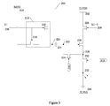
- FIG. 3 is an illustrative circuit diagram showing each pixel unit in a pixel driving circuit of an organic light emitting display device according to a first embodiment of the present disclosure
- FIG. 4 is a waveform diagram showing input signals of the pixel driving circuit of the organic light emitting display device according to the first embodiment of the present disclosure
- FIG. 5 is an illustrative circuit diagram showing each pixel unit in a pixel driving circuit of an organic light emitting display device according to a second embodiment of the present disclosure
- FIG. 6 is a waveform diagram showing input signals of the pixel driving circuit of the organic light emitting display device according to the second embodiment of the present disclosure.
- FIG. 7 is a schematic diagram showing the organic light emitting display device provided by the present disclosure.
- FIG. 3 is an illustrative circuit diagram showing each pixel unit in a pixel driving circuit of an organic light emitting display device according to a first embodiment of the present disclosure.
- the pixel unit 200 includes a control unit 214 , a capacitor 234 , a first transistor 228 , a second transistor 226 , a third transistor 224 , a fourth transistor 230 and a light emitting diode 232 .
- the control unit 214 is coupled with a data line 204 , a common power line 202 , a first scan line 206 and a first node 220 .
- the control unit 214 includes a fifth transistor 216 and a sixth transistor 218 .
- the fifth transistor 216 has a source coupled with the data line 204 , a gate coupled with the first scan line 206 , and a drain coupled with the first node 220 .
- the sixth transistor 218 has a source coupled with the first node 220 , a gate coupled with the first scan line 206 , and a drain coupled with the common power line 202 .
- the fifth transistor 216 has a PMOS structure
- the sixth transistor 218 has a NMOS structure.
- the capacitor 234 is provided with a first sustaining electrode coupled with the first node 220 and a second sustaining electrode coupled with a second node 222 .
- the first transistor 228 is provided with a source, a gate and a drain.
- the source of the first transistor 228 is coupled with the common power line 202
- the gate of the first transistor 228 is coupled with the second scan line 208
- the drain of the first transistor 228 is coupled with the drain of the second transistor 226 .
- the first transistor 228 has a NMOS structure.
- the second transistor 226 is provided with a source, a gate and a drain.
- the source of the second transistor 226 is coupled with a third node 236
- the gate of the second transistor 226 is coupled with the second node 222
- the drain of the second transistor 226 is coupled with the drain of the first transistor 228 .
- the second transistor 226 has a PMOS structure.
- the third transistor 224 is provided with a source, a gate and a drain.
- the source of the third transistor 224 is coupled with the third node 236
- the gate of the third transistor 224 is coupled with a first input terminal 210
- the drain of the third transistor 224 is coupled with the second node 222 .
- the first input terminal 210 is configured to receive a reference signal.
- the third transistor 224 has a PMOS structure.
- the fourth transistor 230 is provided with a source, a gate and a drain.
- the source of the fourth transistor 230 is coupled with the third node 236
- the gate of the fourth transistor 230 is coupled with a second input terminal 212
- the drain of the fourth transistor 230 is coupled with an anode of the light emitting diode 232 .
- the fourth transistor 230 has a PMOS structure.
- the anode of the light emitting diode 232 is coupled with the drain of the fourth transistor 230 , and a cathode of the light emitting diode 232 is grounded.
- the light emitting diode 232 is an organic light emitting diode.
- Each transistor in the present embodiment may be a polysilicon thin film transistor or an amorphous silicon thin film transistor.
- the second transistor 226 is a drive transistor for the pixel unit.
- a voltage between two ends of the capacitor 234 is controlled by a light emitting signal, the reference signal and a scan signal. Further, the current passing through the light emitting diode is not affected by a threshold voltage of the drive transistor.
- the control unit 214 controls a voltage of the first node 220 to be a voltage of the data line 204 or a voltage of the common power line 202 by an input signal from the first scan line 206 .
- the fifth transistor 216 has a PMOS structure
- the sixth transistor 218 has a NMOS structure
- when a high level voltage is applied to the first scan line 206 the fifth transistor 216 is turned off, the sixth transistor 218 is turned on, and the voltage on the common power line 202 is applied to the first node 220 ; and when a low level voltage is applied to the first scan line 206 , the fifth transistor 216 is turned on, the sixth transistor 218 is turned off, and the voltage on the data line 204 is applied to the first node 220 .
- the input signal from the second scan line 208 and the reference signal from the first input terminal 210 are used to control the voltage applied to the second node 222 .
- the variation of each signal within one frame period is divided into three portions.
- the pixel unit is initialized.
- a high level voltage is applied to the first scan line Si, the fifth transistor is turned off, the sixth transistor is turned on, and the voltage V ELVDD on the common power line is applied to the first node, i.e., the first sustaining electrode of the capacitor.
- a low level voltage is applied to the second scan line Si- 1 , and the first transistor is turned off.
- a low level voltage is applied to the reference signal Refi, and the third transistor is turned on.
- a low level voltage is applied to the light emitting signal Emi, and the fourth transistor is turned on.
- the voltage of the second node 222 is equivalent to a voltage when the organic light emitting diode is turned off, i.e., the voltage of the second sustaining electrode of the capacitor is equivalent to the voltage when the organic light emitting diode is turned off.
- a data signal is written into the pixel unit.
- a low level voltage is applied to the first scan line Si, the fifth transistor is turned on, the sixth transistor is turned off, and the voltage V DATA on the data line is applied to the first node, i.e., the first sustaining electrode of the capacitor.
- a high level voltage is applied to the second scan line Si- 1 , and the first transistor is turned on.
- a low level voltage is applied to the reference signal Refi, and the third transistor is turned on.
- a high level voltage is applied to the light emitting signal Emi, and the fourth transistor is turned off.
- the voltage of the second node is the voltage on the common power line being subtracted by a threshold voltage of the second transistor, i.e., V ELVDD ⁇ V th . That is, the voltage of the second sustaining electrode of the capacitor is V ELVDD ⁇ V th , wherein V th is the threshold voltage of the second transistor.
- the pixel unit is controlled to emit light.
- a high level voltage is applied to the first scan line Si, the fifth transistor is turned off, and the sixth transistor is turned on.
- the voltage of the first node is changed from V DATA to V ELVDD . That is, the voltage of the first sustaining electrode of the capacitor is changed from V DATA to V ELVDD .
- a high level voltage is applied to the second scan line Si- 1 , and the first transistor is turned on.
- a high level voltage is applied to the reference signal Refi, and the third transistor is turned off.
- a low level voltage is applied to the light emitting signal Emi, and the fourth transistor is turned on.
- the second transistor is turned on.
- the voltage of the second node is V ELVDD ⁇ V th ⁇ (V DATA ⁇ V ELVDD ). That is, the voltage of the first sustaining electrode of the capacitor is V ELVDD ⁇ V th ⁇ (V DATA ⁇ V ELVDD ).
- I OLED is the current passing through the light emitting diode
- ⁇ 1 ⁇ 2 ⁇ CoxW/L
- V SG is a voltage difference between the source and the drain of the second transistor
- V SG V th +(V DATA ⁇ V ELVDD )
- V th is a threshold voltage of the second transistor.
- the current passing through the light emitting diode is not affected by the threshold voltage of the drive transistor.
- FIG. 5 is an illustrative circuit diagram showing each pixel unit in a pixel driving circuit of an organic light emitting display device according to a second embodiment of the present disclosure.
- the pixel unit 300 includes a control unit 314 , a capacitor 334 , a first transistor 328 , a second transistor 326 , a third transistor 324 , a fourth transistor 330 and a light emitting diode 332 .
- the control unit 314 includes a fifth transistor 316 and a sixth transistor 318 .
- the connection relationships among respective elements thereof are the same as those of the first embodiment shown in FIG. 3 .
- the first transistor 328 , the second transistor 326 , the third transistor 324 , the fourth transistor 330 and the sixth transistor 318 have PMOS structures, and the fifth transistor 316 has a NMOS structure.
- the light emitting diode 332 is an organic light emitting diode.
- each transistor may be a polysilicon thin film transistor or an amorphous silicon thin film transistor.
- the second transistor 326 is a drive transistor for the pixel unit.
- the voltage i.e., the voltage between two ends of the capacitor 334
- the common power line 302 and the ground 338 is controlled by a light emitting signal (from a second input terminal 312 ), a reference signal (a first input terminal 310 ) and signals on the first scan line 306 and the second scan line 308 .
- the current passing through the light emitting diode is not affected by the threshold voltage of the drive transistor.
- the control unit 314 controls a voltage of the first node 320 to be a voltage of the data line 304 or a voltage of the common power line 302 by the input signal from the first scan line 306 .
- the fifth transistor 316 has a NMOS structure
- the sixth transistor 318 has a PMOS structure
- when a high level voltage is applied to the first scan line 306 the fifth transistor 316 is turned on, the sixth transistor 318 is turned off, and the voltage on the data line 304 is applied to the first node 320 ; and when a low level voltage is applied to the first scan line 306 , the fifth transistor 316 is turned off, the sixth transistor 318 is turned on, and the voltage on the common power line 302 is applied to the first node 320 .
- the input signal of from second scan line 308 and the reference signal from the first input terminal 310 control the voltage applied to the second node 322 .
- the variation of each signal within one frame period is divided into three portions.
- the pixel unit is initialized.
- a low level voltage is applied to the first scan line Si, the fifth transistor is turned off, the sixth transistor is turned on, and the voltage V ELVDD on the common power line is applied to the first node, i.e., a first sustaining electrode of the capacitor.
- a high level voltage is applied to the second scan line Si- 1 , and the first transistor is turned off.
- a low level voltage is applied to the reference signal Refi, and the third transistor is turned on.
- a low level voltage is applied to the light emitting signal Emi, and the fourth transistor is turned on.
- the voltage of the second node 322 is equivalent to a voltage when the organic light emitting diode is turned off, i.e., a voltage of the second sustaining electrode of the capacitor is equivalent to the voltage when the organic light emitting diode is turned off.
- the data signal is written into the pixel unit.
- a high level voltage is applied to the first scan line Si, the fifth transistor is turned on, the sixth transistor is turned off, and the voltage V DATA on the data line is applied to the first node, i.e., the first sustaining electrode of the capacitor.
- a low level voltage is applied to the second scan line Si- 1 , and the first transistor is turned on.
- a low level voltage is applied to the reference signal Refi, and the third transistor is turned on.
- a high level voltage is applied to the light emitting signal Emi, and the fourth transistor is turned off.
- the voltage of the second node is the voltage of the common power line being subtracted by a threshold voltage of the second transistor, i.e., V ELVDD ⁇ V th . That is, the voltage of the second sustaining electrode of the capacitor is V ELVDD ⁇ V th , wherein V th is the threshold voltage of the second transistor.
- the pixel unit is controlled to emit light.
- a low level voltage is applied to the first scan line Si, the fifth transistor is turned off, and the sixth transistor is turned on.
- the voltage of the first node is changed from V DATA to V ELVDD . That is, the voltage of the first sustaining electrode of the capacitor is changed from V DATA to V ELVDD .
- a low level voltage is applied to the second scan line Si- 1 , and the first transistor is turned on.
- a high level voltage is applied to the reference signal Refi, and the third transistor is turned off.
- a low level voltage is applied to the light emitting signal Emi, and the fourth transistor is turned on.
- the second transistor is turned on.
- the voltage of the second node is V ELVDD ⁇ V th ⁇ (V DATA ⁇ V ELVDD ). That is, the voltage of the second sustaining electrode of the capacitor is V ELVDD ⁇ V th ⁇ (V DATA ⁇ V ELVDD ).
- I OLED is the current passing through the light emitting diode
- ⁇ 1 ⁇ 2 ⁇ CoxW/L
- V SG is a voltage difference between the source and the drain of the second transistor
- V SG V th +(V DATA ⁇ V ELVDD )
- V th is a threshold voltage of the second transistor.
- the current passing through the light emitting diode is not affected by the threshold voltage of the drive transistor.
- FIG. 7 is a schematic diagram showing the organic light emitting display device provided by the present disclosure.
- the display device includes a plurality of scan lines S 1 to Sn, common power lines intersecting and being insulated from the scan lines and providing a voltage ELVDD, data lines D 1 to Dm intersecting and being insulated from the scan lines, a plurality of pixel units 10 defined by regions surrounded by the plurality of scan lines, the data lines and the common power lines.
- the scan signals on the scan lines S 1 to Sn are controlled by the scan driver 20 .
- the data signals on the data lines D 1 to Dm are controlled by the data driver.
- the present embodiment also shows a light emitting (feedback) signal control driver which is configured to provide corresponding light emitting control signals and feedback signals to respective pixel units 10 .
- the pixel unit PXiiij (the iiij th pixel unit 10 ) receives signals from two scan lines Si and Si- 1 , a feedback signal Refi, a light emitting control signal Emi, and a signal from the data line Dj, and is connected with two potentials ELVDD and ELVSS.
- each pixel unit 10 is shown in FIG. 3 of the first embodiment or in FIG. 5 of the second embodiment.
- the waveforms of the signals from the scan lines Si and Si- 1 , the feedback signal Refi and the light emitting control signal Emi are respectively shown in FIG. 4 of the first embodiment or in FIG. 6 of the second embodiment.
- the organic light emitting display device provided by the present disclosure can effectively compensate the variations of the threshold voltage of the drive thin film transistor, thus prevent nonuniform brightness of a screen due to nonuniform current, and extend lifespan of the screen.
Landscapes
- Engineering & Computer Science (AREA)
- Physics & Mathematics (AREA)
- Computer Hardware Design (AREA)
- General Physics & Mathematics (AREA)
- Theoretical Computer Science (AREA)
- Control Of El Displays (AREA)
- Control Of Indicators Other Than Cathode Ray Tubes (AREA)
- Electroluminescent Light Sources (AREA)
Applications Claiming Priority (3)
| Application Number | Priority Date | Filing Date | Title |
|---|---|---|---|
| CN201310496478.3A CN104575369B (zh) | 2013-10-21 | 2013-10-21 | 像素驱动电路及显示装置 |
| CN201310496478 | 2013-10-21 | ||
| CN201310496478.3 | 2013-10-21 |
Publications (2)
| Publication Number | Publication Date |
|---|---|
| US20150109277A1 US20150109277A1 (en) | 2015-04-23 |
| US9396683B2 true US9396683B2 (en) | 2016-07-19 |
Family
ID=51483288
Family Applications (1)
| Application Number | Title | Priority Date | Filing Date |
|---|---|---|---|
| US14/463,305 Active US9396683B2 (en) | 2013-10-21 | 2014-08-19 | Pixel driving circuit and display device |
Country Status (6)
| Country | Link |
|---|---|
| US (1) | US9396683B2 (zh) |
| EP (1) | EP2863380B1 (zh) |
| JP (1) | JP5899292B2 (zh) |
| KR (1) | KR101496098B1 (zh) |
| CN (1) | CN104575369B (zh) |
| TW (1) | TWI514351B (zh) |
Families Citing this family (4)
| Publication number | Priority date | Publication date | Assignee | Title |
|---|---|---|---|---|
| CN105427795A (zh) * | 2016-01-11 | 2016-03-23 | 京东方科技集团股份有限公司 | 像素驱动电路、方法、像素结构及显示器件 |
| CN105528996B (zh) * | 2016-01-29 | 2018-04-10 | 深圳市华星光电技术有限公司 | 像素补偿电路、方法、扫描驱动电路及平面显示装置 |
| CN107093403B (zh) * | 2017-06-30 | 2019-03-15 | 深圳市华星光电技术有限公司 | 用于oled显示面板的像素驱动电路的补偿方法 |
| US10475385B2 (en) * | 2018-02-28 | 2019-11-12 | Shenzhen China Star Optoelectronics Technology Co., Ltd. | AMOLED pixel driving circuit and driving method capable of ensuring uniform brightness of the organic light emitting diode and improving the display effect of the pictures |
Citations (6)
| Publication number | Priority date | Publication date | Assignee | Title |
|---|---|---|---|---|
| US20050243036A1 (en) * | 2004-04-12 | 2005-11-03 | Kyoji Ikeda | Organic electroluminescence pixel circuit |
| JP2005326828A (ja) | 2004-04-12 | 2005-11-24 | Sanyo Electric Co Ltd | 有機el画素回路 |
| JP2007225738A (ja) | 2006-02-21 | 2007-09-06 | Eastman Kodak Co | 画像表示装置 |
| US20100141644A1 (en) * | 2008-12-05 | 2010-06-10 | Lee Baek-Woon | Display device and method of driving the same |
| US20140166351A1 (en) * | 2012-12-18 | 2014-06-19 | Samsung Electro-Mechanics Co., Ltd. | Multilayer ceramic capacitor and circuit board for mounting the same |
| US20140168180A1 (en) * | 2012-12-13 | 2014-06-19 | Samsung Display Co., Ltd. | Pixel and organic light emitting display device using the same |
Family Cites Families (10)
| Publication number | Priority date | Publication date | Assignee | Title |
|---|---|---|---|---|
| GB0416883D0 (en) * | 2004-07-29 | 2004-09-01 | Koninkl Philips Electronics Nv | Active matrix display devices |
| KR100606416B1 (ko) * | 2004-11-17 | 2006-07-31 | 엘지.필립스 엘시디 주식회사 | 유기전계발광 다이오드의 구동 장치 및 구동방법 |
| KR100703429B1 (ko) * | 2005-08-01 | 2007-04-03 | 삼성에스디아이 주식회사 | 화소 및 이를 이용한 유기 발광 표시장치 |
| KR100822205B1 (ko) * | 2006-10-16 | 2008-04-17 | 삼성에스디아이 주식회사 | 화소 회로 및 그를 포함하는 유기 발광 표시 장치 |
| KR101411752B1 (ko) * | 2008-03-06 | 2014-07-01 | 엘지디스플레이 주식회사 | 유기발광다이오드 표시장치와 그 구동방법 |
| KR101457035B1 (ko) * | 2008-11-13 | 2014-11-03 | 삼성디스플레이 주식회사 | 표시 장치 및 그의 구동 방법 |
| JP5360684B2 (ja) * | 2009-04-01 | 2013-12-04 | セイコーエプソン株式会社 | 発光装置、電子機器および画素回路の駆動方法 |
| KR101768473B1 (ko) * | 2010-10-26 | 2017-08-16 | 엘지디스플레이 주식회사 | 유기발광다이오드 표시장치 및 그 구동방법 |
| CN102760404B (zh) * | 2011-04-28 | 2015-01-28 | 瀚宇彩晶股份有限公司 | 发光二极管显示器像素电路及其驱动方法 |
| CN102654972B (zh) * | 2011-06-21 | 2015-08-12 | 京东方科技集团股份有限公司 | 有源矩阵有机发光二极体面板及其驱动电路与方法 |
-
2013
- 2013-10-21 CN CN201310496478.3A patent/CN104575369B/zh active Active
- 2013-11-14 TW TW102141456A patent/TWI514351B/zh active
-
2014
- 2014-08-05 KR KR20140100522A patent/KR101496098B1/ko active IP Right Grant
- 2014-08-19 US US14/463,305 patent/US9396683B2/en active Active
- 2014-09-04 EP EP14183495.2A patent/EP2863380B1/en active Active
- 2014-10-20 JP JP2014213584A patent/JP5899292B2/ja active Active
Patent Citations (6)
| Publication number | Priority date | Publication date | Assignee | Title |
|---|---|---|---|---|
| US20050243036A1 (en) * | 2004-04-12 | 2005-11-03 | Kyoji Ikeda | Organic electroluminescence pixel circuit |
| JP2005326828A (ja) | 2004-04-12 | 2005-11-24 | Sanyo Electric Co Ltd | 有機el画素回路 |
| JP2007225738A (ja) | 2006-02-21 | 2007-09-06 | Eastman Kodak Co | 画像表示装置 |
| US20100141644A1 (en) * | 2008-12-05 | 2010-06-10 | Lee Baek-Woon | Display device and method of driving the same |
| US20140168180A1 (en) * | 2012-12-13 | 2014-06-19 | Samsung Display Co., Ltd. | Pixel and organic light emitting display device using the same |
| US20140166351A1 (en) * | 2012-12-18 | 2014-06-19 | Samsung Electro-Mechanics Co., Ltd. | Multilayer ceramic capacitor and circuit board for mounting the same |
Non-Patent Citations (1)
| Title |
|---|
| Office Action issued Oct. 6, 2015 by the JP Office. |
Also Published As
| Publication number | Publication date |
|---|---|
| JP2015082113A (ja) | 2015-04-27 |
| US20150109277A1 (en) | 2015-04-23 |
| EP2863380B1 (en) | 2019-05-01 |
| KR101496098B1 (ko) | 2015-02-25 |
| JP5899292B2 (ja) | 2016-04-06 |
| TWI514351B (zh) | 2015-12-21 |
| TW201517001A (zh) | 2015-05-01 |
| EP2863380A1 (en) | 2015-04-22 |
| CN104575369A (zh) | 2015-04-29 |
| CN104575369B (zh) | 2017-07-25 |
Similar Documents
| Publication | Publication Date | Title |
|---|---|---|
| KR101841861B1 (ko) | 유기발광 다이오드의 구동회로 | |
| CN102144293B (zh) | 发光显示装置 | |
| KR101074811B1 (ko) | 화소 회로, 유기전계발광 표시 장치 및 이의 구동 방법 | |
| CN108122500B (zh) | 晶体管基板、有机发光显示面板及有机发光显示装置 | |
| KR101699911B1 (ko) | 유기 발광 표시 장치 | |
| US8368675B2 (en) | Organic light emitting display device | |
| US7009591B2 (en) | Active matrix type display apparatus | |
| KR20110078387A (ko) | 유기 발광장치 및 그 구동방법 | |
| US10565930B2 (en) | Power configuration structure and method for top-emitting AMOLED panel | |
| US9396683B2 (en) | Pixel driving circuit and display device | |
| KR100607513B1 (ko) | 일렉트로-루미네센스 표시장치 및 그 구동방법 | |
| KR100515306B1 (ko) | 유기el 표시패널 | |
| KR100543838B1 (ko) | 일렉트로 루미네센스 표시 장치 | |
| CN111344774B (zh) | 像素电路、显示装置和电子设备 | |
| KR100426132B1 (ko) | 유기전기발광소자 | |
| KR100649559B1 (ko) | Esd 방지 장치 및 이를 구비한 유기 전계 발광 표시 장치 | |
| KR100853538B1 (ko) | 유기전계발광표시장치 | |
| WO2020050252A1 (ja) | 電気光学装置及び電子機器 | |
| KR100640052B1 (ko) | 일렉트로-루미네센스 표시장치 및 그 구동방법 | |
| CN116758863A (zh) | 像素电路、阵列基板和显示面板 | |
| KR20220096869A (ko) | 폴더블 표시 장치 | |
| KR100685851B1 (ko) | 유기전계발광표시장치 | |
| KR102022991B1 (ko) | 유기발광 표시장치 | |
| CN115527479A (zh) | 显示面板和显示装置 | |
| JP2007316512A (ja) | アクティブマトリクス型表示装置 |
Legal Events
| Date | Code | Title | Description |
|---|---|---|---|
| AS | Assignment |
Owner name: EVERDISPLAY OPTRONICS (SHANGHAI) LIMITED, CHINA Free format text: ASSIGNMENT OF ASSIGNORS INTEREST;ASSIGNORS:TSENG, YING-HSIANG;LEE, CHING-HUNG;REEL/FRAME:033566/0036 Effective date: 20140504 |
|
| FEPP | Fee payment procedure |
Free format text: PAYOR NUMBER ASSIGNED (ORIGINAL EVENT CODE: ASPN); ENTITY STATUS OF PATENT OWNER: LARGE ENTITY |
|
| STCF | Information on status: patent grant |
Free format text: PATENTED CASE |
|
| MAFP | Maintenance fee payment |
Free format text: PAYMENT OF MAINTENANCE FEE, 4TH YEAR, LARGE ENTITY (ORIGINAL EVENT CODE: M1551); ENTITY STATUS OF PATENT OWNER: LARGE ENTITY Year of fee payment: 4 |
|
| AS | Assignment |
Owner name: EVERDISPLAY OPTRONICS (SHANGHAI) CO., LTD., CHINA Free format text: CORRECTIVE ASSIGNMENT TO CORRECT THE RECEIVING PARTY DATA PREVIOUSLY RECORDED AT REEL: 033566 FRAME: 0036. ASSIGNOR(S) HEREBY CONFIRMS THE ASSIGNMENT;ASSIGNORS:TSENG, YING-HSIANG;LEE, CHING-HUNG;REEL/FRAME:053558/0957 Effective date: 20140504 |
|
| MAFP | Maintenance fee payment |
Free format text: PAYMENT OF MAINTENANCE FEE, 8TH YEAR, LARGE ENTITY (ORIGINAL EVENT CODE: M1552); ENTITY STATUS OF PATENT OWNER: LARGE ENTITY Year of fee payment: 8 |