US9054214B1 - Methodology of forming CMOS gates on the secondary axis using double-patterning technique - Google Patents
Methodology of forming CMOS gates on the secondary axis using double-patterning technique Download PDFInfo
- Publication number
- US9054214B1 US9054214B1 US14/563,266 US201414563266A US9054214B1 US 9054214 B1 US9054214 B1 US 9054214B1 US 201414563266 A US201414563266 A US 201414563266A US 9054214 B1 US9054214 B1 US 9054214B1
- Authority
- US
- United States
- Prior art keywords
- gate
- core
- gates
- transistors
- trim
- Prior art date
- Legal status (The legal status is an assumption and is not a legal conclusion. Google has not performed a legal analysis and makes no representation as to the accuracy of the status listed.)
- Active
Links
- 238000000034 method Methods 0.000 title claims abstract description 72
- 238000000059 patterning Methods 0.000 title description 3
- 229910021420 polycrystalline silicon Inorganic materials 0.000 claims abstract description 26
- 229920005591 polysilicon Polymers 0.000 claims abstract description 26
- 239000007943 implant Substances 0.000 claims description 146
- 125000001475 halogen functional group Chemical group 0.000 claims description 81
- 238000005286 illumination Methods 0.000 claims description 53
- 239000000758 substrate Substances 0.000 claims description 49
- 238000000206 photolithography Methods 0.000 claims description 43
- 229920002120 photoresistant polymer Polymers 0.000 claims description 42
- 239000004065 semiconductor Substances 0.000 claims description 5
- 238000004519 manufacturing process Methods 0.000 description 12
- VYPSYNLAJGMNEJ-UHFFFAOYSA-N Silicium dioxide Chemical compound O=[Si]=O VYPSYNLAJGMNEJ-UHFFFAOYSA-N 0.000 description 8
- XUIMIQQOPSSXEZ-UHFFFAOYSA-N Silicon Chemical compound [Si] XUIMIQQOPSSXEZ-UHFFFAOYSA-N 0.000 description 7
- 229910003481 amorphous carbon Inorganic materials 0.000 description 7
- 229910052710 silicon Inorganic materials 0.000 description 7
- 239000010703 silicon Substances 0.000 description 7
- 229910052581 Si3N4 Inorganic materials 0.000 description 5
- 229920000620 organic polymer Polymers 0.000 description 5
- HQVNEWCFYHHQES-UHFFFAOYSA-N silicon nitride Chemical compound N12[Si]34N5[Si]62N3[Si]51N64 HQVNEWCFYHHQES-UHFFFAOYSA-N 0.000 description 5
- 239000000463 material Substances 0.000 description 4
- 235000012239 silicon dioxide Nutrition 0.000 description 4
- 239000000377 silicon dioxide Substances 0.000 description 4
- 238000000623 plasma-assisted chemical vapour deposition Methods 0.000 description 3
- 230000005855 radiation Effects 0.000 description 3
- IJGRMHOSHXDMSA-UHFFFAOYSA-N Atomic nitrogen Chemical compound N#N IJGRMHOSHXDMSA-UHFFFAOYSA-N 0.000 description 2
- 238000004380 ashing Methods 0.000 description 2
- 238000000231 atomic layer deposition Methods 0.000 description 2
- 238000005229 chemical vapour deposition Methods 0.000 description 2
- 239000002131 composite material Substances 0.000 description 2
- 239000007789 gas Substances 0.000 description 2
- QJGQUHMNIGDVPM-UHFFFAOYSA-N nitrogen group Chemical group [N] QJGQUHMNIGDVPM-UHFFFAOYSA-N 0.000 description 2
- -1 Inc. Substances 0.000 description 1
- BPQQTUXANYXVAA-UHFFFAOYSA-N Orthosilicate Chemical compound [O-][Si]([O-])([O-])[O-] BPQQTUXANYXVAA-UHFFFAOYSA-N 0.000 description 1
- BLRPTPMANUNPDV-UHFFFAOYSA-N Silane Chemical compound [SiH4] BLRPTPMANUNPDV-UHFFFAOYSA-N 0.000 description 1
- CEPICIBPGDWCRU-UHFFFAOYSA-N [Si].[Hf] Chemical compound [Si].[Hf] CEPICIBPGDWCRU-UHFFFAOYSA-N 0.000 description 1
- 229910052782 aluminium Inorganic materials 0.000 description 1
- XAGFODPZIPBFFR-UHFFFAOYSA-N aluminium Chemical compound [Al] XAGFODPZIPBFFR-UHFFFAOYSA-N 0.000 description 1
- 230000015572 biosynthetic process Effects 0.000 description 1
- 239000013078 crystal Substances 0.000 description 1
- 238000000151 deposition Methods 0.000 description 1
- 230000008021 deposition Effects 0.000 description 1
- 239000003989 dielectric material Substances 0.000 description 1
- 239000012776 electronic material Substances 0.000 description 1
- 238000005516 engineering process Methods 0.000 description 1
- 238000005530 etching Methods 0.000 description 1
- 229910052731 fluorine Inorganic materials 0.000 description 1
- 239000011737 fluorine Substances 0.000 description 1
- 229910052735 hafnium Inorganic materials 0.000 description 1
- VBJZVLUMGGDVMO-UHFFFAOYSA-N hafnium atom Chemical compound [Hf] VBJZVLUMGGDVMO-UHFFFAOYSA-N 0.000 description 1
- 229910000449 hafnium oxide Inorganic materials 0.000 description 1
- WIHZLLGSGQNAGK-UHFFFAOYSA-N hafnium(4+);oxygen(2-) Chemical compound [O-2].[O-2].[Hf+4] WIHZLLGSGQNAGK-UHFFFAOYSA-N 0.000 description 1
- 238000007654 immersion Methods 0.000 description 1
- 239000011810 insulating material Substances 0.000 description 1
- 239000012212 insulator Substances 0.000 description 1
- 150000002500 ions Chemical class 0.000 description 1
- 238000002955 isolation Methods 0.000 description 1
- 229910044991 metal oxide Inorganic materials 0.000 description 1
- 150000004706 metal oxides Chemical class 0.000 description 1
- 229910021421 monocrystalline silicon Inorganic materials 0.000 description 1
- 229910052757 nitrogen Inorganic materials 0.000 description 1
- 229920003986 novolac Polymers 0.000 description 1
- 230000003647 oxidation Effects 0.000 description 1
- 238000007254 oxidation reaction Methods 0.000 description 1
- TWNQGVIAIRXVLR-UHFFFAOYSA-N oxo(oxoalumanyloxy)alumane Chemical compound O=[Al]O[Al]=O TWNQGVIAIRXVLR-UHFFFAOYSA-N 0.000 description 1
- RVTZCBVAJQQJTK-UHFFFAOYSA-N oxygen(2-);zirconium(4+) Chemical compound [O-2].[O-2].[Zr+4] RVTZCBVAJQQJTK-UHFFFAOYSA-N 0.000 description 1
- 229920005989 resin Polymers 0.000 description 1
- 239000011347 resin Substances 0.000 description 1
- 229910000077 silane Inorganic materials 0.000 description 1
- UVGLBOPDEUYYCS-UHFFFAOYSA-N silicon zirconium Chemical compound [Si].[Zr] UVGLBOPDEUYYCS-UHFFFAOYSA-N 0.000 description 1
- 229910001928 zirconium oxide Inorganic materials 0.000 description 1
- GFQYVLUOOAAOGM-UHFFFAOYSA-N zirconium(iv) silicate Chemical compound [Zr+4].[O-][Si]([O-])([O-])[O-] GFQYVLUOOAAOGM-UHFFFAOYSA-N 0.000 description 1
Images


Classifications
-
- H—ELECTRICITY
- H01—ELECTRIC ELEMENTS
- H01L—SEMICONDUCTOR DEVICES NOT COVERED BY CLASS H10
- H01L21/00—Processes or apparatus adapted for the manufacture or treatment of semiconductor or solid state devices or of parts thereof
- H01L21/02—Manufacture or treatment of semiconductor devices or of parts thereof
- H01L21/04—Manufacture or treatment of semiconductor devices or of parts thereof the devices having potential barriers, e.g. a PN junction, depletion layer or carrier concentration layer
- H01L21/18—Manufacture or treatment of semiconductor devices or of parts thereof the devices having potential barriers, e.g. a PN junction, depletion layer or carrier concentration layer the devices having semiconductor bodies comprising elements of Group IV of the Periodic Table or AIIIBV compounds with or without impurities, e.g. doping materials
- H01L21/28—Manufacture of electrodes on semiconductor bodies using processes or apparatus not provided for in groups H01L21/20 - H01L21/268
-
- H—ELECTRICITY
- H01—ELECTRIC ELEMENTS
- H01L—SEMICONDUCTOR DEVICES NOT COVERED BY CLASS H10
- H01L21/00—Processes or apparatus adapted for the manufacture or treatment of semiconductor or solid state devices or of parts thereof
- H01L21/70—Manufacture or treatment of devices consisting of a plurality of solid state components formed in or on a common substrate or of parts thereof; Manufacture of integrated circuit devices or of parts thereof
- H01L21/77—Manufacture or treatment of devices consisting of a plurality of solid state components or integrated circuits formed in, or on, a common substrate
- H01L21/78—Manufacture or treatment of devices consisting of a plurality of solid state components or integrated circuits formed in, or on, a common substrate with subsequent division of the substrate into plural individual devices
- H01L21/82—Manufacture or treatment of devices consisting of a plurality of solid state components or integrated circuits formed in, or on, a common substrate with subsequent division of the substrate into plural individual devices to produce devices, e.g. integrated circuits, each consisting of a plurality of components
- H01L21/822—Manufacture or treatment of devices consisting of a plurality of solid state components or integrated circuits formed in, or on, a common substrate with subsequent division of the substrate into plural individual devices to produce devices, e.g. integrated circuits, each consisting of a plurality of components the substrate being a semiconductor, using silicon technology
- H01L21/8232—Field-effect technology
- H01L21/8234—MIS technology, i.e. integration processes of field effect transistors of the conductor-insulator-semiconductor type
- H01L21/823437—MIS technology, i.e. integration processes of field effect transistors of the conductor-insulator-semiconductor type with a particular manufacturing method of the gate conductors, e.g. particular materials, shapes
- H01L21/823456—MIS technology, i.e. integration processes of field effect transistors of the conductor-insulator-semiconductor type with a particular manufacturing method of the gate conductors, e.g. particular materials, shapes gate conductors with different shapes, lengths or dimensions
-
- H—ELECTRICITY
- H01—ELECTRIC ELEMENTS
- H01L—SEMICONDUCTOR DEVICES NOT COVERED BY CLASS H10
- H01L21/00—Processes or apparatus adapted for the manufacture or treatment of semiconductor or solid state devices or of parts thereof
- H01L21/02—Manufacture or treatment of semiconductor devices or of parts thereof
- H01L21/027—Making masks on semiconductor bodies for further photolithographic processing not provided for in group H01L21/18 or H01L21/34
- H01L21/0271—Making masks on semiconductor bodies for further photolithographic processing not provided for in group H01L21/18 or H01L21/34 comprising organic layers
- H01L21/0273—Making masks on semiconductor bodies for further photolithographic processing not provided for in group H01L21/18 or H01L21/34 comprising organic layers characterised by the treatment of photoresist layers
- H01L21/0274—Photolithographic processes
-
- H—ELECTRICITY
- H01—ELECTRIC ELEMENTS
- H01L—SEMICONDUCTOR DEVICES NOT COVERED BY CLASS H10
- H01L21/00—Processes or apparatus adapted for the manufacture or treatment of semiconductor or solid state devices or of parts thereof
- H01L21/02—Manufacture or treatment of semiconductor devices or of parts thereof
- H01L21/027—Making masks on semiconductor bodies for further photolithographic processing not provided for in group H01L21/18 or H01L21/34
- H01L21/033—Making masks on semiconductor bodies for further photolithographic processing not provided for in group H01L21/18 or H01L21/34 comprising inorganic layers
- H01L21/0332—Making masks on semiconductor bodies for further photolithographic processing not provided for in group H01L21/18 or H01L21/34 comprising inorganic layers characterised by their composition, e.g. multilayer masks, materials
-
- H—ELECTRICITY
- H01—ELECTRIC ELEMENTS
- H01L—SEMICONDUCTOR DEVICES NOT COVERED BY CLASS H10
- H01L21/00—Processes or apparatus adapted for the manufacture or treatment of semiconductor or solid state devices or of parts thereof
- H01L21/02—Manufacture or treatment of semiconductor devices or of parts thereof
- H01L21/027—Making masks on semiconductor bodies for further photolithographic processing not provided for in group H01L21/18 or H01L21/34
- H01L21/033—Making masks on semiconductor bodies for further photolithographic processing not provided for in group H01L21/18 or H01L21/34 comprising inorganic layers
- H01L21/0334—Making masks on semiconductor bodies for further photolithographic processing not provided for in group H01L21/18 or H01L21/34 comprising inorganic layers characterised by their size, orientation, disposition, behaviour, shape, in horizontal or vertical plane
- H01L21/0335—Making masks on semiconductor bodies for further photolithographic processing not provided for in group H01L21/18 or H01L21/34 comprising inorganic layers characterised by their size, orientation, disposition, behaviour, shape, in horizontal or vertical plane characterised by their behaviour during the process, e.g. soluble masks, redeposited masks
-
- H—ELECTRICITY
- H01—ELECTRIC ELEMENTS
- H01L—SEMICONDUCTOR DEVICES NOT COVERED BY CLASS H10
- H01L21/00—Processes or apparatus adapted for the manufacture or treatment of semiconductor or solid state devices or of parts thereof
- H01L21/02—Manufacture or treatment of semiconductor devices or of parts thereof
- H01L21/027—Making masks on semiconductor bodies for further photolithographic processing not provided for in group H01L21/18 or H01L21/34
- H01L21/033—Making masks on semiconductor bodies for further photolithographic processing not provided for in group H01L21/18 or H01L21/34 comprising inorganic layers
- H01L21/0334—Making masks on semiconductor bodies for further photolithographic processing not provided for in group H01L21/18 or H01L21/34 comprising inorganic layers characterised by their size, orientation, disposition, behaviour, shape, in horizontal or vertical plane
- H01L21/0337—Making masks on semiconductor bodies for further photolithographic processing not provided for in group H01L21/18 or H01L21/34 comprising inorganic layers characterised by their size, orientation, disposition, behaviour, shape, in horizontal or vertical plane characterised by the process involved to create the mask, e.g. lift-off masks, sidewalls, or to modify the mask, e.g. pre-treatment, post-treatment
-
- H—ELECTRICITY
- H01—ELECTRIC ELEMENTS
- H01L—SEMICONDUCTOR DEVICES NOT COVERED BY CLASS H10
- H01L21/00—Processes or apparatus adapted for the manufacture or treatment of semiconductor or solid state devices or of parts thereof
- H01L21/02—Manufacture or treatment of semiconductor devices or of parts thereof
- H01L21/027—Making masks on semiconductor bodies for further photolithographic processing not provided for in group H01L21/18 or H01L21/34
- H01L21/033—Making masks on semiconductor bodies for further photolithographic processing not provided for in group H01L21/18 or H01L21/34 comprising inorganic layers
- H01L21/0334—Making masks on semiconductor bodies for further photolithographic processing not provided for in group H01L21/18 or H01L21/34 comprising inorganic layers characterised by their size, orientation, disposition, behaviour, shape, in horizontal or vertical plane
- H01L21/0338—Process specially adapted to improve the resolution of the mask
-
- H—ELECTRICITY
- H01—ELECTRIC ELEMENTS
- H01L—SEMICONDUCTOR DEVICES NOT COVERED BY CLASS H10
- H01L21/00—Processes or apparatus adapted for the manufacture or treatment of semiconductor or solid state devices or of parts thereof
- H01L21/02—Manufacture or treatment of semiconductor devices or of parts thereof
- H01L21/04—Manufacture or treatment of semiconductor devices or of parts thereof the devices having potential barriers, e.g. a PN junction, depletion layer or carrier concentration layer
- H01L21/18—Manufacture or treatment of semiconductor devices or of parts thereof the devices having potential barriers, e.g. a PN junction, depletion layer or carrier concentration layer the devices having semiconductor bodies comprising elements of Group IV of the Periodic Table or AIIIBV compounds with or without impurities, e.g. doping materials
- H01L21/28—Manufacture of electrodes on semiconductor bodies using processes or apparatus not provided for in groups H01L21/20 - H01L21/268
- H01L21/28008—Making conductor-insulator-semiconductor electrodes
-
- H—ELECTRICITY
- H01—ELECTRIC ELEMENTS
- H01L—SEMICONDUCTOR DEVICES NOT COVERED BY CLASS H10
- H01L21/00—Processes or apparatus adapted for the manufacture or treatment of semiconductor or solid state devices or of parts thereof
- H01L21/02—Manufacture or treatment of semiconductor devices or of parts thereof
- H01L21/04—Manufacture or treatment of semiconductor devices or of parts thereof the devices having potential barriers, e.g. a PN junction, depletion layer or carrier concentration layer
- H01L21/18—Manufacture or treatment of semiconductor devices or of parts thereof the devices having potential barriers, e.g. a PN junction, depletion layer or carrier concentration layer the devices having semiconductor bodies comprising elements of Group IV of the Periodic Table or AIIIBV compounds with or without impurities, e.g. doping materials
- H01L21/30—Treatment of semiconductor bodies using processes or apparatus not provided for in groups H01L21/20 - H01L21/26
- H01L21/31—Treatment of semiconductor bodies using processes or apparatus not provided for in groups H01L21/20 - H01L21/26 to form insulating layers thereon, e.g. for masking or by using photolithographic techniques; After treatment of these layers; Selection of materials for these layers
- H01L21/3205—Deposition of non-insulating-, e.g. conductive- or resistive-, layers on insulating layers; After-treatment of these layers
- H01L21/321—After treatment
- H01L21/3213—Physical or chemical etching of the layers, e.g. to produce a patterned layer from a pre-deposited extensive layer
- H01L21/32139—Physical or chemical etching of the layers, e.g. to produce a patterned layer from a pre-deposited extensive layer using masks
-
- H—ELECTRICITY
- H01—ELECTRIC ELEMENTS
- H01L—SEMICONDUCTOR DEVICES NOT COVERED BY CLASS H10
- H01L21/00—Processes or apparatus adapted for the manufacture or treatment of semiconductor or solid state devices or of parts thereof
- H01L21/70—Manufacture or treatment of devices consisting of a plurality of solid state components formed in or on a common substrate or of parts thereof; Manufacture of integrated circuit devices or of parts thereof
- H01L21/77—Manufacture or treatment of devices consisting of a plurality of solid state components or integrated circuits formed in, or on, a common substrate
- H01L21/78—Manufacture or treatment of devices consisting of a plurality of solid state components or integrated circuits formed in, or on, a common substrate with subsequent division of the substrate into plural individual devices
- H01L21/82—Manufacture or treatment of devices consisting of a plurality of solid state components or integrated circuits formed in, or on, a common substrate with subsequent division of the substrate into plural individual devices to produce devices, e.g. integrated circuits, each consisting of a plurality of components
- H01L21/822—Manufacture or treatment of devices consisting of a plurality of solid state components or integrated circuits formed in, or on, a common substrate with subsequent division of the substrate into plural individual devices to produce devices, e.g. integrated circuits, each consisting of a plurality of components the substrate being a semiconductor, using silicon technology
- H01L21/8232—Field-effect technology
- H01L21/8234—MIS technology, i.e. integration processes of field effect transistors of the conductor-insulator-semiconductor type
- H01L21/823412—MIS technology, i.e. integration processes of field effect transistors of the conductor-insulator-semiconductor type with a particular manufacturing method of the channel structures, e.g. channel implants, halo or pocket implants, or channel materials
-
- H—ELECTRICITY
- H01—ELECTRIC ELEMENTS
- H01L—SEMICONDUCTOR DEVICES NOT COVERED BY CLASS H10
- H01L21/00—Processes or apparatus adapted for the manufacture or treatment of semiconductor or solid state devices or of parts thereof
- H01L21/70—Manufacture or treatment of devices consisting of a plurality of solid state components formed in or on a common substrate or of parts thereof; Manufacture of integrated circuit devices or of parts thereof
- H01L21/77—Manufacture or treatment of devices consisting of a plurality of solid state components or integrated circuits formed in, or on, a common substrate
- H01L21/78—Manufacture or treatment of devices consisting of a plurality of solid state components or integrated circuits formed in, or on, a common substrate with subsequent division of the substrate into plural individual devices
- H01L21/82—Manufacture or treatment of devices consisting of a plurality of solid state components or integrated circuits formed in, or on, a common substrate with subsequent division of the substrate into plural individual devices to produce devices, e.g. integrated circuits, each consisting of a plurality of components
- H01L21/822—Manufacture or treatment of devices consisting of a plurality of solid state components or integrated circuits formed in, or on, a common substrate with subsequent division of the substrate into plural individual devices to produce devices, e.g. integrated circuits, each consisting of a plurality of components the substrate being a semiconductor, using silicon technology
- H01L21/8232—Field-effect technology
- H01L21/8234—MIS technology, i.e. integration processes of field effect transistors of the conductor-insulator-semiconductor type
- H01L21/823462—MIS technology, i.e. integration processes of field effect transistors of the conductor-insulator-semiconductor type with a particular manufacturing method of the gate insulating layers, e.g. different gate insulating layer thicknesses, particular gate insulator materials or particular gate insulator implants
-
- H—ELECTRICITY
- H01—ELECTRIC ELEMENTS
- H01L—SEMICONDUCTOR DEVICES NOT COVERED BY CLASS H10
- H01L21/00—Processes or apparatus adapted for the manufacture or treatment of semiconductor or solid state devices or of parts thereof
- H01L21/70—Manufacture or treatment of devices consisting of a plurality of solid state components formed in or on a common substrate or of parts thereof; Manufacture of integrated circuit devices or of parts thereof
- H01L21/77—Manufacture or treatment of devices consisting of a plurality of solid state components or integrated circuits formed in, or on, a common substrate
- H01L21/78—Manufacture or treatment of devices consisting of a plurality of solid state components or integrated circuits formed in, or on, a common substrate with subsequent division of the substrate into plural individual devices
- H01L21/82—Manufacture or treatment of devices consisting of a plurality of solid state components or integrated circuits formed in, or on, a common substrate with subsequent division of the substrate into plural individual devices to produce devices, e.g. integrated circuits, each consisting of a plurality of components
- H01L21/822—Manufacture or treatment of devices consisting of a plurality of solid state components or integrated circuits formed in, or on, a common substrate with subsequent division of the substrate into plural individual devices to produce devices, e.g. integrated circuits, each consisting of a plurality of components the substrate being a semiconductor, using silicon technology
- H01L21/8232—Field-effect technology
- H01L21/8234—MIS technology, i.e. integration processes of field effect transistors of the conductor-insulator-semiconductor type
- H01L21/8238—Complementary field-effect transistors, e.g. CMOS
- H01L21/823814—Complementary field-effect transistors, e.g. CMOS with a particular manufacturing method of the source or drain structures, e.g. specific source or drain implants or silicided source or drain structures or raised source or drain structures
-
- H—ELECTRICITY
- H01—ELECTRIC ELEMENTS
- H01L—SEMICONDUCTOR DEVICES NOT COVERED BY CLASS H10
- H01L21/00—Processes or apparatus adapted for the manufacture or treatment of semiconductor or solid state devices or of parts thereof
- H01L21/70—Manufacture or treatment of devices consisting of a plurality of solid state components formed in or on a common substrate or of parts thereof; Manufacture of integrated circuit devices or of parts thereof
- H01L21/77—Manufacture or treatment of devices consisting of a plurality of solid state components or integrated circuits formed in, or on, a common substrate
- H01L21/78—Manufacture or treatment of devices consisting of a plurality of solid state components or integrated circuits formed in, or on, a common substrate with subsequent division of the substrate into plural individual devices
- H01L21/82—Manufacture or treatment of devices consisting of a plurality of solid state components or integrated circuits formed in, or on, a common substrate with subsequent division of the substrate into plural individual devices to produce devices, e.g. integrated circuits, each consisting of a plurality of components
- H01L21/822—Manufacture or treatment of devices consisting of a plurality of solid state components or integrated circuits formed in, or on, a common substrate with subsequent division of the substrate into plural individual devices to produce devices, e.g. integrated circuits, each consisting of a plurality of components the substrate being a semiconductor, using silicon technology
- H01L21/8232—Field-effect technology
- H01L21/8234—MIS technology, i.e. integration processes of field effect transistors of the conductor-insulator-semiconductor type
- H01L21/8238—Complementary field-effect transistors, e.g. CMOS
- H01L21/823828—Complementary field-effect transistors, e.g. CMOS with a particular manufacturing method of the gate conductors, e.g. particular materials, shapes
- H01L21/82385—Complementary field-effect transistors, e.g. CMOS with a particular manufacturing method of the gate conductors, e.g. particular materials, shapes gate conductors with different shapes, lengths or dimensions
-
- H—ELECTRICITY
- H01—ELECTRIC ELEMENTS
- H01L—SEMICONDUCTOR DEVICES NOT COVERED BY CLASS H10
- H01L21/00—Processes or apparatus adapted for the manufacture or treatment of semiconductor or solid state devices or of parts thereof
- H01L21/70—Manufacture or treatment of devices consisting of a plurality of solid state components formed in or on a common substrate or of parts thereof; Manufacture of integrated circuit devices or of parts thereof
- H01L21/77—Manufacture or treatment of devices consisting of a plurality of solid state components or integrated circuits formed in, or on, a common substrate
- H01L21/78—Manufacture or treatment of devices consisting of a plurality of solid state components or integrated circuits formed in, or on, a common substrate with subsequent division of the substrate into plural individual devices
- H01L21/82—Manufacture or treatment of devices consisting of a plurality of solid state components or integrated circuits formed in, or on, a common substrate with subsequent division of the substrate into plural individual devices to produce devices, e.g. integrated circuits, each consisting of a plurality of components
- H01L21/822—Manufacture or treatment of devices consisting of a plurality of solid state components or integrated circuits formed in, or on, a common substrate with subsequent division of the substrate into plural individual devices to produce devices, e.g. integrated circuits, each consisting of a plurality of components the substrate being a semiconductor, using silicon technology
- H01L21/8232—Field-effect technology
- H01L21/8234—MIS technology, i.e. integration processes of field effect transistors of the conductor-insulator-semiconductor type
- H01L21/8238—Complementary field-effect transistors, e.g. CMOS
- H01L21/823857—Complementary field-effect transistors, e.g. CMOS with a particular manufacturing method of the gate insulating layers, e.g. different gate insulating layer thicknesses, particular gate insulator materials or particular gate insulator implants
-
- H—ELECTRICITY
- H01—ELECTRIC ELEMENTS
- H01L—SEMICONDUCTOR DEVICES NOT COVERED BY CLASS H10
- H01L27/00—Devices consisting of a plurality of semiconductor or other solid-state components formed in or on a common substrate
- H01L27/02—Devices consisting of a plurality of semiconductor or other solid-state components formed in or on a common substrate including semiconductor components specially adapted for rectifying, oscillating, amplifying or switching and having potential barriers; including integrated passive circuit elements having potential barriers
- H01L27/0203—Particular design considerations for integrated circuits
- H01L27/0207—Geometrical layout of the components, e.g. computer aided design; custom LSI, semi-custom LSI, standard cell technique
Definitions
- This invention relates to the field of integrated circuits. More particularly, this invention relates to photolithography processes used to form integrated circuits.
- An integrated circuit at the 28 nanometer node or beyond containing core metal oxide semiconductor (MOS) transistors which operate at a core voltage, for example 1 to 1.5 volts, and input/output (I/O) MOS transistors which operate at a higher I/O voltage, for example, 1.8 to 2.5 volts, is fabricated using photolithography process with a 193 nanometer light source. Forming the core transistors and the I/O transistors while maintaining a fabrication cost and complexity of the integrated circuit at or below a desired level is problematic.
- MOS metal oxide semiconductor
- I/O input/output
- An integrated circuit containing core transistors and I/O transistors oriented perpendicular to the core transistors is formed by exposing a gate etch mask layer stack through a gate pattern photomask including core transistor gates and oversized I/O transistor gates. Core transistor gate lengths are defined by the gate pattern photomask.
- a first gate hardmask etch process removes the gate hardmask layer in exposed areas. The process continues with exposing a gate trim mask layer stack through a gate trim photomask. I/O gate lengths are defined by the gate trim photomask.
- a second gate hardmask etch process removes the gate hardmask layer in exposed areas.
- a gate etch operation removes polysilicon exposed by the gate hardmask layer to form gates for the core transistors and I/O transistors.
- the integrated circuit may also include I/O transistors oriented parallel to the core transistors, with gate lengths defined by the gate pattern photomask.
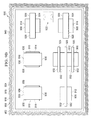
- FIG. 1 depicts an example illumination source having a dipole component for photolithographic processes which may be used to form integrated circuits as described herein.
- FIG. 2 depicts an example pattern formed by an illumination source with a strong dipole component, such as illumination source, oriented as depicted in FIG. 1 .
- FIG. 3 depicts an example composite dipole-quadrupole-octopole off-axis illumination source having a moderate dipole component for photolithographic processes which may be used to form integrated circuits as described herein.
- FIG. 4 depicts an example pattern formed by an illumination source with a moderate dipole component, such as illumination source, oriented as depicted in FIG. 3 .
- FIG. 5A through FIG. 5G are top views of an integrated circuit with core MOS transistors oriented in one direction and I/O MOS transistors oriented perpendicular to the core transistors, formed according to an example, depicted in successive stages of fabrication.
- FIG. 5H through FIG. 5J depict alternative halo implant operations for the integrated circuit described in reference to FIG. 5A through FIG. 5E .
- FIG. 6 depicts an alternate gate trim photolithography operation using a clear geometry gate trim photomask.
- FIG. 7A through FIG. 7D are cross sections depicting the first gate hardmask etch process.
- FIG. 8A through FIG. 8D are cross sections depicting the second gate hardmask etch process.
- FIG. 9A through FIG. 9G are top views of an integrated circuit with core MOS transistors oriented in one direction, a first plurality of I/O MOS transistors oriented parallel to the core transistors and a second plurality of I/O MOS transistors oriented perpendicular to the core transistors, formed according to an example, depicted in successive stages of fabrication.
- FIG. 9H through FIG. 9K depict alternative halo implant operations for the integrated circuit described in reference to FIG. 9A through FIG. 9F .
- FIG. 1 depicts an example illumination source having a strong dipole component for photolithographic processes which may be used to form integrated circuits as described herein.
- the illumination source 100 is configured with two off axis dipole region emitting regions 102 , so that the illumination source 100 has a strong dipole component.
- the illumination source 100 may provide, for example, 193 nanometer radiation, and may be used in an immersion photolithography tool which can resolve parallel equally spaced lines aligned with the dipole component of the illumination source 100 having a line/space pitch distance of 80 nanometers.
- FIG. 2 depicts an example pattern formed by an illumination source with a strong dipole component, such as illumination source 100 , oriented as depicted in FIG. 1 .
- the pattern 200 includes a first plurality of minimum pitch equally spaced parallel lines 202 oriented with the strong dipole component of the illumination source 100 , and a second plurality of minimum pitch equally spaced lines 204 aligned perpendicular to the dipole component.
- a first minimum line/space pitch distance 206 of the first plurality of equally spaced parallel lines 202 is significantly smaller, for example by a factor of three, than a second minimum line/space pitch distance 208 of the second plurality of equally spaced parallel lines 204 , due to the strong dipole component.
- the illumination source may provide 193 nanometer radiation, and the illumination source dipole component may be configured so that the first minimum line/space pitch distance 206 is 80 nanometers and the second minimum line/space pitch distance 208 is 240 nanometers.
- FIG. 3 depicts an example composite dipole-quadrupole-octopole off-axis illumination source 300 having a moderate dipole component for photolithographic processes which may be used to form integrated circuits as described herein.
- the moderate dipole illumination source 300 is configured with two strong emitting regions 302 along the vertical direction, two moderate emitting regions 304 along the horizontal direction, and four weak emitting regions 306 along diagonal directions.
- FIG. 4 depicts an example pattern formed by an illumination source with a moderate dipole component, such as illumination source 300 , oriented as depicted in FIG. 3 .
- the pattern 400 includes a first plurality of minimum pitch distance equally spaced parallel lines 402 oriented with the moderate dipole component of the illumination source 300 , and a second plurality of minimum pitch distance equally spaced lines 404 aligned perpendicular to the dipole component.
- a first minimum line/space pitch distance 406 of the first plurality of equally spaced parallel lines 402 is smaller, for example by a factor of one and one-half, than a second minimum line/space pitch distance 408 of the second plurality of equally spaced parallel lines 404 , due to the moderate dipole component.
- the illumination source may provide 193 nanometer radiation, and the illumination source dipole component may be configured so that the first minimum line/space pitch distance 406 is 115 nanometers and the second minimum line/space pitch distance 408 is 170 nanometers.
- FIG. 5A through FIG. 5G are top views of an integrated circuit with core MOS transistors oriented in one direction and I/O MOS transistors oriented perpendicular to the core transistors, formed according to an example, depicted in successive stages of fabrication.
- the integrated circuit 500 is formed in and on a semiconductor substrate 502 , for example, a single crystal silicon wafer, a silicon-on-insulator (SOI) wafer, a hybrid orientation technology (HOT) wafer with regions of different crystal orientations, a silicon wafer with an epitaxial layer, or other material appropriate for fabrication of the integrated circuit 500 .
- a layer of field oxide 504 is formed at a top surface of the substrate 502 .
- the field oxide 504 may be, for example, silicon dioxide between 250 and 400 nanometers thick, formed by a shallow trench isolation (STI) process.
- An STI process may include the steps of: forming an oxide layer on the substrate 502 , forming a silicon nitride layer on the oxide layer, patterning the silicon nitride layer so as to expose an area for the field oxide 504 , etching a trench in the substrate 502 in the exposed area to an appropriate depth for a desired thickness of the field oxide 504 , growing a layer of thermal oxide on sidewalls and a bottom of the trench, filling the trench with silicon dioxide by chemical vapor deposition (CVD), high density plasma (HDP) or high aspect ratio process (HARP), removing unwanted silicon dioxide from a top surface of the silicon nitride layer, and removing the silicon nitride layer.
- CVD chemical vapor deposition
- HDP high density plasma
- HTP high aspect ratio process
- a first plurality of openings 506 in the field oxide 504 provide core active areas 506 for the core transistors, and a second plurality of openings 508 provide I/O active areas 508 for the I/O transistors.
- a core gate dielectric layer 510 is formed at the top surface of the substrate 502 in the core active areas 506
- an I/O gate dielectric layer 512 is formed at the top surface of the substrate 502 in the I/O active areas 508 .
- the I/O gate dielectric layer 512 may be formed concurrently with, and be a same thickness as, the core gate dielectric layer 510 .
- the core gate dielectric layer 510 and the I/O gate dielectric layer 512 may be formed concurrently to be one or more layers of silicon dioxide, silicon oxy-nitride, aluminum oxide, aluminum oxy-nitride, hafnium oxide, hafnium silicate, hafnium silicon oxy-nitride, zirconium oxide, zirconium silicate, zirconium silicon oxy-nitride, a combination of the aforementioned materials, or other insulating material.
- the core gate dielectric layer 510 and the I/O gate dielectric layer 512 may include nitrogen as a result of exposure to a nitrogen containing plasma or a nitrogen containing ambient gas at temperatures between 50 C. and 800 C.
- the core gate dielectric layer 510 and the I/O gate dielectric layer 512 may be 1 to 4 nanometers thick.
- the core gate dielectric layer 510 and the I/O gate dielectric layer 512 may be formed by any of a variety of gate dielectric formation processes, for example thermal oxidation, plasma nitridation of an oxide layer, and/or dielectric material deposition by atomic layer deposition (ALD).
- ALD atomic layer deposition
- the I/O gate dielectric layer 512 may be formed separately from the core gate dielectric layer 510 so that the I/O gate dielectric layer 512 is thicker than the core gate dielectric layer 510 .
- I/O gate dielectric layer 512 may be at least 11 ⁇ 2 times thicker than the core gate dielectric layer 510 .
- the I/O gate dielectric layer 512 may be formed in two stages, so that a second of the two stages is formed concurrently with the core gate dielectric layer 510 .
- a gate layer stack 514 is formed over the field oxide 504 , the core gate dielectric layer 510 and the I/O gate dielectric layer 512 .
- the gate layer stack 514 includes a bottom layer of polysilicon 30 to 60 nanometers thick, and a gate hardmask layer, for example silicon nitride 60 to 80 nanometers thick, over the polysilicon layer.
- the bottom layer of polysilicon may be formed, for example, by thermally decomposing silane gas inside a low-pressure reactor at a temperature between 580° C. to 650° C.
- the gate hardmask layer may be formed, for example, using a plasma enhanced chemical vapor deposition (PECVD) process.
- PECVD plasma enhanced chemical vapor deposition
- a gate etch pattern stack 516 is formed over the gate layer stack 514 .
- the gate etch pattern stack 516 may include, for example, a layer of amorphous carbon hardmask 60 to 120 nanometers thick over the gate layer stack 514 .
- the amorphous carbon hardmask may be, for example, a layer of Advanced Patterning Film (APF) from Applied Materials, Inc., Or a layer of Ashable Hardmask (AHM) from Novellus Systems, Inc.
- the gate etch pattern stack 516 may further include a layer of dielectric hardmask such as 20 to 40 nanometers of silicon oxynitride formed by PECVD.
- the gate etch pattern stack 516 may further include a layer of organic bottom anti-reflection coat (BARC) such as 20 to 40 nanometers of a spin-on BARC.
- BARC organic bottom anti-reflection coat
- the gate etch pattern stack 516 has a top layer of photoresist, such as an amplified positive tone resist sensitive to 193 nanometer illumination.
- FIG. 1 A gate pattern photolithography operation is performed which uses an illumination source with a strong dipole component, for example as described in reference to FIG.
- gate pattern photomask 520 a first gate photomask 520 , referred to as gate pattern photomask 520 , with dark geometries, to expose the gate etch pattern stack 516 outside of areas for gates of the core transistors and I/O transistors.
- the dark geometries of the gate pattern photomask 520 include core gate geometries 524 in areas defined for gates of the core transistors.
- the core gate geometries 524 are oriented with the strong dipole component of the illumination source 518 as described in reference to FIG. 2 , so that edges 526 of the core gate geometries 524 define gate lengths of the core transistors.
- the gate pattern photomask 520 also includes I/O gate geometries 528 in areas defined for gates of the I/O transistors.
- the I/O gate geometries 528 are oriented perpendicular to the core gate geometries 524 .
- Ends 530 of the I/O gate geometries 528 define ends for the I/O transistors.
- Edges 532 of the I/O gate geometries 528 oriented perpendicular to the strong dipole component of the illumination source 518 are oversized for the I/O transistors, for example by 20 nanometers.
- the gate pattern photomask 520 may further include an optional border 534 .
- a positive tone develop operation is performed which leaves photoresist of the gate etch pattern stack 516 in areas defined by the dark geometries of the gate pattern photomask 520 .
- the developed photoresist areas of the gate etch pattern stack 516 include core pattern portions 536 over the core active areas 506 .
- the core pattern portions 536 have edges 538 which define gate lengths of the core transistors.
- the developed photoresist areas of the gate etch pattern stack 516 also include I/O pattern portions 540 over the I/O active areas 508 .
- the I/O pattern portions 540 have edges 542 which may exhibit undesired wavy contours as depicted in FIG. 5C as a result of “ringing” during exposure with the gate pattern strong dipole illumination source.
- a first gate hardmask etch process is performed which transfers the pattern of the developed photoresist of the gate etch pattern stack 516 to the gate hardmask layer of the gate layer stack 514 by removing the gate hardmask layer under areas exposed by the developed photoresist.
- the first gate hardmask etch process is depicted in cross section for an instance of the core transistors in FIG. 7A through FIG. 7D . Steps of the first gate hardmask etch process for the I/O transistors and elsewhere on the integrated circuit 500 follow a similar recital. Referring to FIG. 7A , the integrated circuit 500 has the core gate dielectric layer 510 over the substrate 502 .
- the gate layer stack 514 includes the bottom layer of polysilicon 544 over the core gate dielectric layer 510 and the gate hardmask layer 546 over the polysilicon 544 .
- the gate etch pattern stack 516 includes the layer of amorphous carbon hardmask 548 over the gate hardmask layer 546 , the layer of dielectric hardmask 550 over the layer of amorphous carbon hardmask 548 , the layer of BARC 552 over the layer of dielectric hardmask 550 , and the core pattern portions 536 of the developed photoresist areas.
- a first etch step of the first gate hardmask etch process is performed which removes the layer of BARC 552 and the layer of dielectric hardmask 550 in areas exposed by the core pattern portions 536 of the developed photoresist areas. At least a portion of the core pattern portions 536 of the developed photoresist is removed by the first etch step.
- a second etch step of the first gate hardmask etch process is performed which removes the layer of amorphous carbon hardmask 548 in areas exposed by the dielectric hardmask 550 . Remaining portions of the core pattern portions 536 of the developed photoresist and the layer of BARC 552 may be removed by the second etch step.
- a third etch step of the first gate hardmask etch process is performed which removes the gate hardmask layer 546 in areas exposed by the amorphous carbon hardmask 548 . Remaining portions of the dielectric hardmask 550 may be removed by the third etch step. After the third etch step is completed, remaining amorphous carbon hardmask 548 is removed, for example by ashing.
- Fabrication of the integrated circuit 500 continues with reference to FIG. 5D .
- Core transistor portions 554 and I/O transistor portions 556 of the gate hardmask layer 546 are depicted with a coarse stipple pattern.
- a tri-layer gate trim pattern stack 558 is formed over the gate layer stack 514 .
- the gate trim pattern stack 558 includes a spin-on layer of organic polymer such as novolak resin 80 to 180 nanometers thick over the gate layer stack 514 .
- the gate trim pattern stack 558 further includes a layer of 20 to 40 nanometers of spin-on silicon-containing hardmask available from Brewer Science, Inc., Dow corning Corporation, JSR Corporation, AZ Electronic Materials, and other suppliers of lithographic materials.
- the gate trim pattern stack 558 has a top layer of amplified positive tone 193 nanometer sensitive photoresist.
- a gate trim photolithography operation is performed which uses an illumination source with a moderate dipole component, for example as described in reference to FIG. 3 and oriented as depicted by example illumination source 560 , or possibly an isotropic illumination source.
- the gate trim photolithography operation uses a dark geometry second gate photomask 562 , referred to as a dark geometry gate trim photomask 562 , which has dark geometries, to expose the gate trim pattern stack 558 so as to define edges of the I/O transistor gates which were oversized by the gate pattern photolithography operation.
- the dark geometries of the gate trim photomask 562 include dark core end trim areas 564 and dark I/O gate edge trim areas 566 .
- the gate trim photolithography operation exposes the gate trim pattern stack 558 outside the core end trim areas 564 to define ends of core gate areas, and exposes the gate trim pattern stack 558 outside the I/O gate edge trim areas 566 to define edges for gate lengths of the I/O transistors.
- a negative tone develop operation is performed which removes the top layer of photoresist in the gate trim pattern stack 558 from the areas exposed by the gate trim photolithography operation, that is areas outside the dark geometries of the dark geometry gate trim photomask 562 .
- an alternate gate trim photolithography operation may use a clear geometry gate trim photomask 568 as depicted in FIG. 6 .
- the clear geometry gate trim photomask 568 has clear geometries including clear core end trim areas 570 and clear I/O gate edge trim areas 572 .
- the gate trim photolithography operation exposes the gate trim pattern stack 558 in the clear core end trim areas 570 to define ends of core gate areas, and exposes the gate trim pattern stack 558 in the clear I/O gate edge trim areas 572 to define edges for gate lengths of the I/O transistors.
- a negative tone develop operation is performed which removes the top layer of photoresist in the gate trim pattern stack 558 from the areas exposed by the alternate gate trim photolithography operation, that is areas in the dark geometries of the clear geometry gate trim photomask 568 .
- Developed photoresist 574 from the gate trim photolithography operation discussed in reference to FIG. 5D , or the alternate gate trim photolithography operation discussed in reference to FIG. 6 is depicted in FIG. 5E with a light stipple pattern.
- Open areas in the developed photoresist 574 include core end trim areas 576 exposing the core transistor portions 554 of the gate hardmask layer 546 and I/O gate edge trim areas 578 exposing the I/O transistor portions 556 of the gate hardmask layer 546 .
- a second gate hardmask etch process is performed which transfers the pattern of the developed photoresist 574 of the gate trim pattern stack 558 to the gate hardmask layer 546 of the gate layer stack 514 by removing the gate hardmask layer 546 under areas exposed by the developed photoresist 574 .
- the second gate hardmask etch process is depicted in cross section for an instance of the core transistors in FIG. 8A through FIG. 8D . Steps of the second gate hardmask etch process for the I/O transistors and elsewhere on the integrated circuit 500 follow a similar recital. Referring to FIG. 8A , the integrated circuit 500 has the core gate dielectric layer 510 over the substrate 502 .
- the gate layer stack 514 includes the bottom layer of polysilicon 544 over the core gate dielectric layer 510 and the gate hardmask layer 546 over the polysilicon 544 .
- the gate trim pattern stack 558 includes the layer of spin-on organic polymer 580 over the gate hardmask layer 546 , the layer of spin-on silicon-containing hardmask 582 over the layer of spin-on organic polymer 580 , and the developed photoresist 574 .
- a first etch step of the second gate hardmask etch process is performed which removes the layer of spin-on silicon-containing hardmask 582 in the core end trim areas 576 of the developed photoresist 574 . At least a portion of the developed photoresist 574 is removed by the first etch step.
- a second etch step of the second gate hardmask etch process is performed which removes the layer of spin-on organic polymer 580 in the core end trim areas 576 .
- the developed photoresist 574 may be removed by the second etch step.
- a third etch step of the second gate hardmask etch process is performed which removes the gate hardmask layer 546 in the core end trim areas 576 .
- the layer of spin-on silicon-containing hardmask 582 is removed by the third etch step.
- remaining spin-on organic polymer 580 is removed, for example by ashing.
- the etched gate hardmask layer 546 defines areas for a subsequent gate etch process, as shown in FIG. 5 F.
- the bottom layer of polysilicon 544 of the gate layer stack 514 extends across the integrated circuit 500 .
- the etched gate hardmask layer 546 includes core gate mask portions 584 and I/O gate mask portions 586 .
- the core gate mask portions 584 have edges 588 which were defined by the gate pattern photolithography operation and which in turn define gate lengths of the core transistors.
- the I/O gate mask portions 586 have edges 592 which were defined by the gate trim photolithography operation and which in turn define gate lengths of the I/O transistors.
- a gate etch operation is performed which removes polysilicon from the bottom layer of polysilicon 544 of the gate layer stack 514 outside the etched gate hardmask layer 546 to form core gates 596 and I/O gates 598 .
- the etched gate hardmask layer 546 of FIG. 5F is depicted in FIG. 5G in outline.
- the gate etch operation may include one or more steps using a reactive ion etch (RIE) process which provides fluorine radicals to remove the polysilicon.
- RIE reactive ion etch
- the gate etch operation may undercut the etched gate hardmask layer 546 so that final lateral dimensions of the core gates 596 and I/O gates 598 are less than lateral dimensions of the etched gate hardmask layer 546 , as depicted in FIG. 5G .
- the core gate dielectric layer 510 and the I/O gate dielectric layer 512 may be removed by the gate etch operation outside the core gates 596 and the I/O gates 598 .
- a line/space pitch distance 590 of the core gates 596 may be 78 to 86 nanometers, and a linewidth 594 of the I/O gates 598 may be 110 to 130 nanometers. In a further version, the linewidth 594 of the I/O gates 598 may be 78 to 82 nanometers.
- FIG. 5H through FIG. 5J depict alternative halo implant operations for the integrated circuit 500 .
- a first halo implant operation includes a core transistor halo implant process having two angled implant steps 600 aligned perpendicular to the core gates 596 over the core active areas 506 .
- the core transistors 602 and possibly the I/O transistors 604 are exposed to the angled implant steps 600 . Exposing the I/O transistors 604 to the angled implant steps 600 may allow a single implant mask to be used for lightly doped drain (LDD) implants in both the core transistors 602 and the I/O transistors 604 , advantageously reducing fabrication cost and complexity of the integrated circuit 500 .
- LDD lightly doped drain
- the two angled implants 600 form core halo implanted regions 606 in the substrate 502 extending a short distance under the core gates 596 .
- no angled halo implants are aligned perpendicular to the I/O gates 598 over the I/O active areas 508 .
- the first halo operation does not form I/O halo implanted regions under the I/O gates 598 , so that a desired on-state current in the I/O transistors 604 may be attained.
- a second halo implant operation includes a combined core and I/O transistor halo implant process having four angled implant steps 610 with equal doses. Two angled implant steps 610 of the four angled implant steps 610 are aligned perpendicular to the core gates 596 over the core active areas 506 , and two angled implant steps 610 of the four angled implant steps 610 are aligned perpendicular to the I/O gates 598 over the I/O active areas 508 .
- the core transistors 602 and the I/O transistors 604 are exposed to the four angled implant steps 610 , allowing a single implant mask to be used for LDD implants in both the core transistors 602 and the I/O transistors 604 , advantageously reducing fabrication cost and complexity of the integrated circuit 500 .
- the two angled implant steps 610 aligned perpendicular to the core gates 596 form core halo implanted regions 606 in the substrate 502 extending a short distance under the core gates 596
- the two angled implant steps 610 aligned perpendicular to the I/O gates 598 form I/O halo implanted regions 608 in the substrate 502 extending a short distance under the I/O gates 598 .
- Forming the I/O halo implanted regions 608 extending under the I/O gates 598 may provide an off-state leakage current below a desired limit in the I/O transistors 604 .
- a third halo implant operation includes a combined core and I/O transistor halo implant process having four angled implant steps with unequal doses.
- Two high dose angled implant steps 612 of the four angled implant steps are aligned perpendicular to the core gates 596 over the core active areas 506
- two low dose angled implant steps 614 of the four angled implant steps are aligned perpendicular to the I/O gates 598 over the I/O active areas 508 .
- a dose of the two low dose angled implant steps may be less than half a dose of the two high dose angled implant steps.
- the core transistors 602 and the I/O transistors 604 are exposed to the high dose angled implant steps 612 and the low dose angled implant steps 614 , allowing a single implant mask to be used for LDD implants in both the core transistors 602 and the I/O transistors 604 , advantageously reducing fabrication cost and complexity of the integrated circuit 500 .
- the two high dose angled implants 612 form core halo implanted regions 606 in the substrate 502 extending a short distance under the core gates 596
- the two low dose angled implants 614 form I/O halo implanted regions 608 in the substrate 502 extending a short distance under the I/O gates 598 .
- Forming the I/O halo implanted regions 608 extending under the I/O gates 598 with a lower dose than the core halo implants 612 may provide a desired balance between on-state current and off-state leakage current in the I/O transistors 604 .
- FIG. 9A through FIG. 9G are top views of an integrated circuit with core MOS transistors oriented in one direction, a first plurality of I/O MOS transistors oriented parallel to the core transistors and a second plurality of I/O MOS transistors oriented perpendicular to the core transistors, formed according to an example, depicted in successive stages of fabrication.
- the integrated circuit 900 is formed in and on a semiconductor substrate 902 , and a layer of field oxide 904 is formed at a top surface of the substrate 902 , as described in reference to FIG. 5A .
- a first plurality of openings 906 in the field oxide 904 provide core active areas 906 for the core transistors, a second plurality of openings 908 provide a first plurality of I/O active areas 908 for the first plurality of I/O transistors oriented parallel to the core transistors, and a third plurality of openings 910 provide a second plurality of I/O active areas 910 for the second plurality of I/O transistors oriented perpendicular to the core transistors.
- a core gate dielectric layer 912 is formed at a top surface of the substrate 902 in the core active areas 906
- an I/O gate dielectric layer 914 is formed at the top surface of the substrate 902 in the first plurality of I/O active areas 908 and in the second plurality of I/O active areas 910 .
- the I/O gate dielectric layer 914 may be formed concurrently with, and be a same thickness as, the core gate dielectric layer 912 , or may be thicker than the core gate dielectric layer 912 , as described in reference to FIG. 5A .
- a gate layer stack 916 is formed over the field oxide 904 , the core gate dielectric layer 912 and the I/O gate dielectric layer 914 .
- the gate layer stack 916 includes a bottom layer of polysilicon and a gate hardmask layer over the polysilicon layer, as described in reference to FIG. 5A .
- Features such as the core active areas 906 , the first plurality of I/O active areas 908 and the second plurality of I/O active areas 910 under the gate layer stack 916 are depicted with solid lines to improve clarity of the Figures.
- a gate etch pattern stack 918 is formed over the gate layer stack 916 as described in reference to FIG. 5B .
- Features such as the core active areas 906 , the first plurality of I/O active areas 908 and the second plurality of I/O active areas 910 under the gate etch pattern stack 918 are depicted with solid lines to improve clarity of the Figures.
- a gate pattern photolithography operation is performed which uses an illumination source with a strong dipole component, for example as described and oriented in FIG.
- the gate pattern photomask 924 includes core gate geometries 926 in areas defined for gates of the core transistors, first I/O gate geometries 928 in areas defined for gates of the first plurality of I/O transistors oriented parallel to the core transistors, and second I/O gate geometries 930 in areas defined for gates of the second plurality of I/O transistors oriented perpendicular to the core transistors.
- the core gate geometries 926 are oriented with the strong dipole component of the illumination source as described in reference to FIG. 2 , so that edges 932 of the core gate geometries 926 define gate lengths of the core transistors. Similarly, edges 934 of the first I/O gate geometries 928 define gate lengths of the first plurality of I/O transistors. Ends 936 of the second I/O gate geometries 930 define ends of the second plurality of I/O transistors. Edges 938 of the second I/O gate geometries 930 are oversized for the second plurality of I/O transistors, for example by 20 nanometers.
- the gate pattern photomask 924 may further include an optional border 940 .
- a positive tone develop operation is performed which leaves photoresist of the gate etch pattern stack 918 in areas defined by the dark geometries of the gate pattern photomask 924 .
- the developed photoresist areas of the gate etch pattern stack 918 include core pattern portions 942 over the core active areas 906 .
- the core pattern portions 942 have edges 948 which define gate lengths of the core transistors.
- the developed photoresist areas of the gate etch pattern stack 918 also include first I/O pattern portions 944 over the first plurality of I/O active areas 908 .
- the first I/O pattern portions 944 have edges 950 which define gate lengths of the first I/O transistors.
- the developed photoresist areas of the gate etch pattern stack 918 further include second I/O pattern portions 946 over the first plurality of I/O active areas 908 .
- the second I/O pattern portions 946 have edges 952 which may exhibit undesired wavy contours as depicted in FIG. 9C as a result of “ringing” during exposure with the gate pattern strong dipole illumination source.
- a first gate hardmask etch process as described in reference to FIG. 7A through FIG. 7D , is performed which transfers the pattern of the developed photoresist areas of the gate etch pattern stack 918 to the gate hardmask layer of the gate layer stack 916 .
- core transistor portions 954 , first I/O transistor portions 956 and second I/O transistor portions 958 of the gate hardmask layer of the gate layer stack 916 are depicted with a coarse stipple pattern.
- a tri-layer gate trim pattern stack 960 is formed over the gate layer stack 916 , as described in reference to FIG. 5D .
- a gate trim photolithography operation is performed which uses an illumination source with a moderate dipole component, for example as described in reference to FIG. 3 and oriented as depicted by example illumination source 962 , or possibly an isotropic illumination source.
- the gate trim photolithography operation uses a dark geometry second gate trim photomask 964 which has dark geometries, to expose the gate trim pattern stack 960 so as to define edges of the second I/O transistor gates which were oversized by the gate pattern photolithography operation.
- the dark geometries of the gate trim photomask 964 include dark core end trim areas 966 , dark first I/O end trim areas 968 and dark second I/O gate edge trim areas 970 .
- the gate trim photolithography operation exposes the gate trim pattern stack 960 .
- a negative tone develop operation is performed which removes the top layer of photoresist in the gate trim pattern stack 960 from the areas exposed by the gate trim photolithography operation, that is areas outside the dark geometries of the dark geometry gate trim photomask 964 .
- Open areas in the developed photoresist 972 include core end trim areas 974 exposing the core transistor portions 554 of the gate hardmask layer of the gate layer stack 916 , first I/O end trim areas 976 exposing the first I/O transistor portions 956 of the gate hardmask layer, and second I/O gate edge trim areas 978 exposing the second I/O transistor portions 958 of the gate hardmask layer.
- a second gate hardmask etch process is performed which transfers the pattern of the developed photoresist 972 of the gate trim pattern stack 960 to the gate hardmask layer of the gate layer stack 916 , as described in reference to FIG. 8A through FIG. 8D .
- the etched gate hardmask layer 980 of the gate layer stack 916 defines areas for a subsequent gate etch process, as shown in FIG. 9F .
- the bottom layer of polysilicon 982 of the gate layer stack 916 extends across the integrated circuit 900 .
- the etched gate hardmask layer 980 includes core hardmask portions 984 , first I/O hardmask portions 986 and second I/O hardmask portions 988 .
- the core hardmask portions 984 have edges 990 which were defined by the gate pattern photolithography operation and which in turn define gate lengths of the core transistors.
- the first I/O hardmask portions 986 have edges 992 which were defined by the gate pattern photolithography operation and which in turn define gate lengths of the first I/O transistors.
- the second I/O hardmask portions 988 have edges 994 which were defined by the gate trim photolithography operation and which in turn define gate lengths of the second I/O transistors.
- a gate etch operation as described in reference to FIG. 5G is performed which removes polysilicon from the bottom layer of polysilicon 982 of the gate layer stack 916 outside the etched gate hardmask layer 980 of FIG. 9F to form core gates 996 , first I/O gates 998 and second I/O gates 1000 .
- the etched gate hardmask layer 980 is depicted in FIG. 9G in outline.
- the gate etch operation may undercut the etched gate hardmask layer 980 so that final lateral dimensions of the core gates 996 , first I/O gates 998 and second I/O gates 1000 are less than lateral dimensions of the etched gate hardmask layer 980 , as depicted in FIG. 9G .
- the core gate dielectric layer 912 and the I/O gate dielectric layer 914 may be removed by the gate etch operation outside the core gates 996 , first I/O gates 998 and second I/O gates 1000 .
- a line/space pitch distance 1002 of the core gates 996 may be 78 to 86 nanometers
- a linewidth 1004 of the first I/O gates 998 and a linewidth 1006 of the second I/O gates 1000 may be 110 to 130 nanometers.
- the linewidth 1004 of the first I/O gates 998 and the linewidth 1006 of the second I/O gates 1000 may be 78 to 82 nanometers.
- FIG. 9H through FIG. 9K depict alternative halo implant operations for the integrated circuit 900 .
- a first halo implant operation includes a core transistor halo implant process having two angled implant steps 1008 aligned perpendicular to the core gates 996 over the core active areas 906 .
- the core transistors 1010 are exposed to the angled implant steps 1008 , while the first I/O transistors 1012 and the second I/O transistors 1014 are blocked from the angled implant steps 1008 , for example by an implant mask of photoresist.
- the two angled implants 1008 form core halo implanted regions 1016 in the substrate 902 extending a short distance under the core gates 996 .
- Exposing core transistors 1010 to the angled implant steps 1008 may limit an off-state current of the core transistors 1010 to a desired value.
- no angled halo implants are aligned perpendicular to the first I/O gates 998 over the first plurality of I/O active areas 908 or to the second I/O gates 1000 over the second plurality of I/O active areas 910 .
- the first halo operation does not form halo implanted regions under the first I/O gates 998 or the second I/O gates 1000 , which may provide a desired on-state current in the first I/O transistors 1012 and the second I/O transistors 1014 .
- a second halo implant operation includes a combined core and I/O transistor halo implant process having four angled implant steps 1020 with equal doses.
- Two angled implant steps 1020 of the four angled implant steps 1020 are aligned perpendicular to the core gates 996 over the core active areas 906 and perpendicular to the first I/O gates 998 over the first plurality of I/O active areas 908 , and the remaining two angled implant steps 1020 of the four angled implant steps 1020 are aligned perpendicular to the second I/O gates 1000 over the second plurality of I/O active areas 910 .
- the core transistors 1010 , the first I/O transistors 1012 and the second I/O transistors 1014 are exposed to the angled implant steps 1020 , allowing a single implant mask to be used for LDD implants in both the core transistors 1010 , the first I/O transistors 1012 and the second I/O transistors 1014 , advantageously reducing fabrication cost and complexity of the integrated circuit 900 .
- the two angled implants 1020 aligned perpendicular to the core gates 996 and the first I/O gates 998 form core halo implanted regions 1016 in the substrate 902 extending a short distance under the core gates 996 and I/O halo implanted regions 1018 extending a short distance under the first I/O gates 998 , respectively.
- the two angled implants 1020 aligned perpendicular to the second I/O gates 1000 form additional instances of the I/O halo implanted regions 1018 in the substrate 902 extending a short distance under the second I/O gates 1000 .
- Forming the I/O halo implanted regions 1018 extending under the first I/O gates 998 and the second I/O gates 1000 may provide an off-state leakage current below a desired limit in the first I/O transistors 1012 and the second I/O transistors 1014 .
- a third halo implant operation includes separate core and I/O transistor halo implant process having two angled implant steps 1022 with a core dose for the core transistors 1010 and four angled implant steps 1024 with an I/O dose for the first I/O transistors 1012 and the second I/O transistors 1014 .
- the I/O dose may be less than half of the core dose.
- the first I/O transistors 1012 and the second I/O transistors 1014 are blocked from the two angled implant steps 1022 with the core dose, for example by an implant mask.
- the two core dose angled implants 1022 form core halo implanted regions 1016 in the substrate 902 extending a short distance under the core gates 996 .
- the two I/O dose angled implants 1024 aligned perpendicular to the first I/O gates form I/O halo implanted regions 1018 in the substrate 902 extending a short distance under the first I/O gates 998
- the two I/O dose angled implants 1024 aligned perpendicular to the second I/O gates 1000 form additional instances of the I/O halo implanted regions 1018 in the substrate 902 extending a short distance under the second I/O gates 1000 .
- Forming the halo implanted regions 1018 extending under the first I/O gates 998 and the second I/O gates 1000 with a separate dose from the core halo implants 1022 may provide a desired balance between on-state current and off-state leakage current in the first I/O transistors 1012 and the second I/O transistors 1014 .
- a fourth halo implant operation includes a core transistor halo implant process having two angled implant steps 1026 aligned perpendicular to the core gates 996 over the core active areas 906 and the first I/O gates 998 over the first I/I active areas 908 .
- the two angled implants 1026 form core halo implanted regions 1016 in the substrate 902 extending a short distance under the core gates 996 and I/O halo implanted regions 1018 extending a short distance under the first I/O gates 998 , respectively.
- no angled halo implants are aligned perpendicular to the second I/O gates 1000 over the second plurality of I/O active areas 910 , so that the fourth halo operation does not form I/O halo implanted regions under the second I/O gates 1000 .
- Forming the I/O halo implanted regions 1018 extending under the first I/O gates 998 may provide an off-state leakage current below a desired limit in the first I/O transistors 1012 , while forming the second I/O transistors 1014 having no I/O halo implanted regions may provide a desired on-state current in the second I/O transistors 1014 .
- Exposing the second I/O transistors 1014 to the angled implant steps 1026 may allow a single implant mask to be used for LDD implants in the core transistors 1010 , the first I/O transistors 1012 and the second I/O transistors 1014 , advantageously reducing fabrication cost and complexity of the integrated circuit 900 .
Landscapes
- Engineering & Computer Science (AREA)
- Power Engineering (AREA)
- Physics & Mathematics (AREA)
- Condensed Matter Physics & Semiconductors (AREA)
- General Physics & Mathematics (AREA)
- Computer Hardware Design (AREA)
- Microelectronics & Electronic Packaging (AREA)
- Manufacturing & Machinery (AREA)
- Inorganic Chemistry (AREA)
- Chemical & Material Sciences (AREA)
- General Engineering & Computer Science (AREA)
- Metal-Oxide And Bipolar Metal-Oxide Semiconductor Integrated Circuits (AREA)
- Insulated Gate Type Field-Effect Transistor (AREA)
Priority Applications (1)
| Application Number | Priority Date | Filing Date | Title |
|---|---|---|---|
| US14/563,266 US9054214B1 (en) | 2013-12-12 | 2014-12-08 | Methodology of forming CMOS gates on the secondary axis using double-patterning technique |
Applications Claiming Priority (2)
| Application Number | Priority Date | Filing Date | Title |
|---|---|---|---|
| US201361915102P | 2013-12-12 | 2013-12-12 | |
| US14/563,266 US9054214B1 (en) | 2013-12-12 | 2014-12-08 | Methodology of forming CMOS gates on the secondary axis using double-patterning technique |
Publications (2)
| Publication Number | Publication Date |
|---|---|
| US9054214B1 true US9054214B1 (en) | 2015-06-09 |
| US20150170971A1 US20150170971A1 (en) | 2015-06-18 |
Family
ID=53267986
Family Applications (1)
| Application Number | Title | Priority Date | Filing Date |
|---|---|---|---|
| US14/563,266 Active US9054214B1 (en) | 2013-12-12 | 2014-12-08 | Methodology of forming CMOS gates on the secondary axis using double-patterning technique |
Country Status (2)
| Country | Link |
|---|---|
| US (1) | US9054214B1 (zh) |
| CN (1) | CN104716031B (zh) |
Cited By (3)
| Publication number | Priority date | Publication date | Assignee | Title |
|---|---|---|---|---|
| US10229854B1 (en) | 2017-12-14 | 2019-03-12 | International Business Machines Corporation | FinFET gate cut after dummy gate removal |
| US10236219B1 (en) | 2017-11-22 | 2019-03-19 | International Business Machines Corporation | VFET metal gate patterning for vertical transport field effect transistor |
| US20220231014A1 (en) * | 2021-01-18 | 2022-07-21 | Taiwan Semiconductor Manufacturing Company Ltd. | Dummy device for core device to operate in a safe operating area and method for manufacturing the same |
Families Citing this family (1)
| Publication number | Priority date | Publication date | Assignee | Title |
|---|---|---|---|---|
| KR102564551B1 (ko) * | 2016-01-26 | 2023-08-04 | 삼성전자주식회사 | 반도체 소자의 제조 방법 |
Citations (5)
| Publication number | Priority date | Publication date | Assignee | Title |
|---|---|---|---|---|
| US6465307B1 (en) * | 2001-11-30 | 2002-10-15 | Texas Instruments Incorporated | Method for manufacturing an asymmetric I/O transistor |
| US7984393B2 (en) * | 2007-11-14 | 2011-07-19 | Texas Instruments Incorporated | System and method for making photomasks |
| US8373441B1 (en) * | 2011-09-20 | 2013-02-12 | Lsi Corporation | Orienting voltage translators in input/output buffers |
| US20140252485A1 (en) * | 2013-03-07 | 2014-09-11 | Texas Instruments Incorporated | Low-Cost CMOS Structure with Dual Gate Dielectrics and Method of Forming the CMOS Structure |
| US20140284725A1 (en) * | 2013-03-25 | 2014-09-25 | Texas Instruments Incorporated | MOS Transistor Structure and Method of Forming the Structure with Vertically and Horizontally-Elongated Metal Contacts |
Family Cites Families (4)
| Publication number | Priority date | Publication date | Assignee | Title |
|---|---|---|---|---|
| US6924199B2 (en) * | 2003-11-21 | 2005-08-02 | Taiwan Semiconductor Manufacturing Co., Ltd. | Method to form flash memory with very narrow polysilicon spacing |
| CN100527356C (zh) * | 2007-01-12 | 2009-08-12 | 联华电子股份有限公司 | 修整硬掩模层的方法、形成晶体管栅极的方法和堆叠结构 |
| US8268712B2 (en) * | 2010-05-27 | 2012-09-18 | United Microelectronics Corporation | Method of forming metal gate structure and method of forming metal gate transistor |
| CN102479693B (zh) * | 2010-11-30 | 2013-11-06 | 中芯国际集成电路制造(北京)有限公司 | 形成栅极的方法 |
-
2014
- 2014-12-08 US US14/563,266 patent/US9054214B1/en active Active
- 2014-12-11 CN CN201410764481.3A patent/CN104716031B/zh active Active
Patent Citations (5)
| Publication number | Priority date | Publication date | Assignee | Title |
|---|---|---|---|---|
| US6465307B1 (en) * | 2001-11-30 | 2002-10-15 | Texas Instruments Incorporated | Method for manufacturing an asymmetric I/O transistor |
| US7984393B2 (en) * | 2007-11-14 | 2011-07-19 | Texas Instruments Incorporated | System and method for making photomasks |
| US8373441B1 (en) * | 2011-09-20 | 2013-02-12 | Lsi Corporation | Orienting voltage translators in input/output buffers |
| US20140252485A1 (en) * | 2013-03-07 | 2014-09-11 | Texas Instruments Incorporated | Low-Cost CMOS Structure with Dual Gate Dielectrics and Method of Forming the CMOS Structure |
| US20140284725A1 (en) * | 2013-03-25 | 2014-09-25 | Texas Instruments Incorporated | MOS Transistor Structure and Method of Forming the Structure with Vertically and Horizontally-Elongated Metal Contacts |
Cited By (6)
| Publication number | Priority date | Publication date | Assignee | Title |
|---|---|---|---|---|
| US10236219B1 (en) | 2017-11-22 | 2019-03-19 | International Business Machines Corporation | VFET metal gate patterning for vertical transport field effect transistor |
| US10615082B2 (en) | 2017-11-22 | 2020-04-07 | International Business Machines Corporation | VFET metal gate patterning for vertical transport field effect transistor |
| US10229854B1 (en) | 2017-12-14 | 2019-03-12 | International Business Machines Corporation | FinFET gate cut after dummy gate removal |
| US10600868B2 (en) | 2017-12-14 | 2020-03-24 | Tessera, Inc. | FinFET gate cut after dummy gate removal |
| US11024715B2 (en) | 2017-12-14 | 2021-06-01 | Tessera, Inc. | FinFET gate cut after dummy gate removal |
| US20220231014A1 (en) * | 2021-01-18 | 2022-07-21 | Taiwan Semiconductor Manufacturing Company Ltd. | Dummy device for core device to operate in a safe operating area and method for manufacturing the same |
Also Published As
| Publication number | Publication date |
|---|---|
| CN104716031B (zh) | 2019-07-19 |
| US20150170971A1 (en) | 2015-06-18 |
| CN104716031A (zh) | 2015-06-17 |
Similar Documents
| Publication | Publication Date | Title |
|---|---|---|
| US10727135B2 (en) | FinFET with sloped surface at interface between isolation structures and manufacturing method thereof | |
| US8802510B2 (en) | Methods for controlling line dimensions in spacer alignment double patterning semiconductor processing | |
| US8058161B2 (en) | Recessed STI for wide transistors | |
| US11145519B2 (en) | Mechanisms for forming patterns using multiple lithography processes | |
| US11145510B2 (en) | FinFET device over convex insulating structure | |
| US9875906B2 (en) | Mechanisms for forming patterns using multiple lithography processes | |
| US10586709B2 (en) | Methods of fabricating semiconductor devices | |
| CN103247575B (zh) | 鳍式场效应晶体管(FinFET)器件的图案化工艺 | |
| TW201719755A (zh) | 特徵尺寸縮減技術(二) | |
| US9054214B1 (en) | Methodology of forming CMOS gates on the secondary axis using double-patterning technique | |
| US10153166B2 (en) | Mechanisms for forming patterns using lithography processes | |
| US8753938B2 (en) | Method for 1/F noise reduction in NMOS devices | |
| US8202791B2 (en) | Method for generating two dimensions for different implant energies | |
| US7651947B2 (en) | Mask forming and implanting methods using implant stopping layer and mask so formed | |
| US20090325106A1 (en) | Method for Implant Imaging with Spin-on Hard Masks | |
| Hopf et al. | CMOS patterning over high-aspect ratio topographies for N10/N7 using spin-on carbon hardmasks | |
| US9362275B1 (en) | Semiconductor device with dummy gate structures | |
| KR101012240B1 (ko) | 반도체 소자의 제조 방법 | |
| JP2008071951A (ja) | 半導体装置の製造方法 |
Legal Events
| Date | Code | Title | Description |
|---|---|---|---|
| AS | Assignment |
Owner name: TEXAS INSTRUMENTS INCORPORATED, TEXAS Free format text: ASSIGNMENT OF ASSIGNORS INTEREST;ASSIGNORS:BALDWIN, GREGORY CHARLES;JESSEN, SCOTT WILLIAM;SIGNING DATES FROM 20150107 TO 20150114;REEL/FRAME:034796/0880 |
|
| STCF | Information on status: patent grant |
Free format text: PATENTED CASE |
|
| MAFP | Maintenance fee payment |
Free format text: PAYMENT OF MAINTENANCE FEE, 4TH YEAR, LARGE ENTITY (ORIGINAL EVENT CODE: M1551); ENTITY STATUS OF PATENT OWNER: LARGE ENTITY Year of fee payment: 4 |
|
| MAFP | Maintenance fee payment |
Free format text: PAYMENT OF MAINTENANCE FEE, 8TH YEAR, LARGE ENTITY (ORIGINAL EVENT CODE: M1552); ENTITY STATUS OF PATENT OWNER: LARGE ENTITY Year of fee payment: 8 |