US8991333B2 - Substrate processing method and system - Google Patents

Substrate processing method and system Download PDF

Info

Publication number
US8991333B2
US8991333B2 US13/292,518 US201113292518A US8991333B2 US 8991333 B2 US8991333 B2 US 8991333B2 US 201113292518 A US201113292518 A US 201113292518A US 8991333 B2 US8991333 B2 US 8991333B2
Authority
US
United States
Prior art keywords
gas
fluorine
target substrate
chamber
gas supply
Prior art date
Legal status (The legal status is an assumption and is not a legal conclusion. Google has not performed a legal analysis and makes no representation as to the accuracy of the status listed.)
Expired - Fee Related, expires
Application number
US13/292,518
Other versions
US20120055401A1 (en
Inventor
Shigeki Tozawa
Current Assignee (The listed assignees may be inaccurate. Google has not performed a legal analysis and makes no representation or warranty as to the accuracy of the list.)
Tokyo Electron Ltd
Original Assignee
Tokyo Electron Ltd
Priority date (The priority date is an assumption and is not a legal conclusion. Google has not performed a legal analysis and makes no representation as to the accuracy of the date listed.)
Filing date
Publication date
Application filed by Tokyo Electron Ltd filed Critical Tokyo Electron Ltd
Priority to US13/292,518 priority Critical patent/US8991333B2/en
Publication of US20120055401A1 publication Critical patent/US20120055401A1/en
Application granted granted Critical
Publication of US8991333B2 publication Critical patent/US8991333B2/en
Expired - Fee Related legal-status Critical Current
Adjusted expiration legal-status Critical

Links

Images

Classifications

    • HELECTRICITY
    • H01ELECTRIC ELEMENTS
    • H01LSEMICONDUCTOR DEVICES NOT COVERED BY CLASS H10
    • H01L21/00Processes or apparatus adapted for the manufacture or treatment of semiconductor or solid state devices or of parts thereof
    • HELECTRICITY
    • H01ELECTRIC ELEMENTS
    • H01LSEMICONDUCTOR DEVICES NOT COVERED BY CLASS H10
    • H01L21/00Processes or apparatus adapted for the manufacture or treatment of semiconductor or solid state devices or of parts thereof
    • H01L21/02Manufacture or treatment of semiconductor devices or of parts thereof
    • H01L21/02041Cleaning
    • H01L21/02057Cleaning during device manufacture
    • H01L21/0206Cleaning during device manufacture during, before or after processing of insulating layers
    • H01L21/02063Cleaning during device manufacture during, before or after processing of insulating layers the processing being the formation of vias or contact holes
    • HELECTRICITY
    • H01ELECTRIC ELEMENTS
    • H01LSEMICONDUCTOR DEVICES NOT COVERED BY CLASS H10
    • H01L21/00Processes or apparatus adapted for the manufacture or treatment of semiconductor or solid state devices or of parts thereof
    • H01L21/67Apparatus specially adapted for handling semiconductor or electric solid state devices during manufacture or treatment thereof; Apparatus specially adapted for handling wafers during manufacture or treatment of semiconductor or electric solid state devices or components ; Apparatus not specifically provided for elsewhere
    • H01L21/67005Apparatus not specifically provided for elsewhere
    • H01L21/67011Apparatus for manufacture or treatment
    • H01L21/67155Apparatus for manufacturing or treating in a plurality of work-stations
    • H01L21/67161Apparatus for manufacturing or treating in a plurality of work-stations characterized by the layout of the process chambers
    • H01L21/67173Apparatus for manufacturing or treating in a plurality of work-stations characterized by the layout of the process chambers in-line arrangement
    • HELECTRICITY
    • H01ELECTRIC ELEMENTS
    • H01LSEMICONDUCTOR DEVICES NOT COVERED BY CLASS H10
    • H01L21/00Processes or apparatus adapted for the manufacture or treatment of semiconductor or solid state devices or of parts thereof
    • H01L21/67Apparatus specially adapted for handling semiconductor or electric solid state devices during manufacture or treatment thereof; Apparatus specially adapted for handling wafers during manufacture or treatment of semiconductor or electric solid state devices or components ; Apparatus not specifically provided for elsewhere
    • H01L21/67005Apparatus not specifically provided for elsewhere
    • H01L21/67011Apparatus for manufacture or treatment
    • H01L21/67155Apparatus for manufacturing or treating in a plurality of work-stations
    • H01L21/6719Apparatus for manufacturing or treating in a plurality of work-stations characterized by the construction of the processing chambers, e.g. modular processing chambers
    • HELECTRICITY
    • H01ELECTRIC ELEMENTS
    • H01LSEMICONDUCTOR DEVICES NOT COVERED BY CLASS H10
    • H01L21/00Processes or apparatus adapted for the manufacture or treatment of semiconductor or solid state devices or of parts thereof
    • H01L21/67Apparatus specially adapted for handling semiconductor or electric solid state devices during manufacture or treatment thereof; Apparatus specially adapted for handling wafers during manufacture or treatment of semiconductor or electric solid state devices or components ; Apparatus not specifically provided for elsewhere
    • H01L21/67005Apparatus not specifically provided for elsewhere
    • H01L21/67011Apparatus for manufacture or treatment
    • H01L21/67155Apparatus for manufacturing or treating in a plurality of work-stations
    • H01L21/67201Apparatus for manufacturing or treating in a plurality of work-stations characterized by the construction of the load-lock chamber
    • HELECTRICITY
    • H01ELECTRIC ELEMENTS
    • H01LSEMICONDUCTOR DEVICES NOT COVERED BY CLASS H10
    • H01L21/00Processes or apparatus adapted for the manufacture or treatment of semiconductor or solid state devices or of parts thereof
    • H01L21/70Manufacture or treatment of devices consisting of a plurality of solid state components formed in or on a common substrate or of parts thereof; Manufacture of integrated circuit devices or of parts thereof
    • H01L21/71Manufacture of specific parts of devices defined in group H01L21/70
    • H01L21/768Applying interconnections to be used for carrying current between separate components within a device comprising conductors and dielectrics
    • H01L21/76897Formation of self-aligned vias or contact plugs, i.e. involving a lithographically uncritical step

Abstract

A substrate processing method includes a first step of subjecting a target substrate to a gas process within an atmosphere containing a fluorine-containing process gas, thereby forming a fluorine-containing reaction product on a surface of the target substrate. The method further includes a second step of subjecting the target substrate treated by the gas process to a heating process and a gas process within an atmosphere containing a reactive gas that reacts with fluorine.

Description

CROSS REFERENCE TO RELATED APPLICATION
This application is a continuation of Ser. No. 12/314,933 filed Dec. 18, 2008 and which is being incorporated in its entirety herein by reference.
BACKGROUND OF THE INVENTION
1. Field of the Invention
The present invention relates to a substrate processing method and substrate processing system for performing a gas process on a target substrate, such as a semiconductor wafer, while supplying a process gas onto the target substrate, and also to a computer readable storage medium that stores a program for controlling the substrate processing system.
2. Description of the Related Art
In recent years, in the process of manufacturing semiconductor devices, a method called “chemical oxide removal (COR) process” has attracted attention as a method alternative to dry etching or wet etching for realizing a fine etching process.
As a method of this kind for etching a silicon dioxide (SiO2) film formed on the surface of a target object, such as a semiconductor wafer, the following process is known (for example, see US 2004/0182417 A1, US 2004/0184792 A1, and Jpn. Pat. Appln. KOKAI Publication No. 2005-39185). Specifically, while the temperature of the target object is adjusted under a vacuum state, a mixture gas of hydrogen fluoride (HF) gas and ammonia (NH3) gas is supplied into a chamber. The mixture gas reacts with the silicon dioxide and generates ammonium fluorosilicate ((NH4)2SiF6). The ammonium fluorosilicate is heated and thereby sublimed in the subsequent step, so that the silicon dioxide film is consumed and etched from the surface.
In recent years, since semiconductor devices are being miniaturized, the integration level of semiconductor integrated circuit devices is being increased. With an increase in the level of miniaturization and integration, the size of contact holes formed in semiconductor integrated circuit device chips becomes smaller and the number of contact holes formed in each chip becomes larger.
The COR described above is effective for removing a silicon dioxide film formed at the bottom of contact holes, i.e., a so-called natural oxide film, which has been generated in forming the holes.
However, as the size of contact holes is smaller and the number of contact holes is larger, fluorine and/or fluorine compound are more likely to be left as residues in the contact holes. If a reactive halogen and/or halogen compound, particularly fluorine and/or fluorine compound, are left in the contact holes, they may cause abnormal reactions with components of integrated circuits, such as a silicon substrate, gate electrodes, gate electrode sidewall insulating films, inter-level insulating films, and interconnection layers. Such abnormal reactions deteriorate the yield of semiconductor integrated circuit devices.
BRIEF SUMMARY OF THE INVENTION
An object of the present invention is to provide a substrate processing method and substrate processing system that can decrease the probability of abnormal reactions being caused and thereby maintain and improve the characteristic and yield of semiconductor integrated circuit devices, and further to provide a computer readable storage medium that stores a program for controlling the substrate processing system.
According to a first aspect of the present invention, there is provided a substrate processing method comprising: a first step of subjecting a target substrate to a gas process within an atmosphere containing a fluorine-containing process gas, thereby forming a fluorine-containing reaction product on a surface of the target substrate; and a second step of subjecting the target substrate treated by the gas process to a heating process and a gas process within an atmosphere containing a reactive gas that reacts with fluorine.
According to a second aspect of the present invention, there is provided a substrate processing system comprising: a gas process section including a process gas supply section for supplying a fluorine-containing process gas, the gas process section being configured to subject a target substrate to a gas process within an atmosphere containing the fluorine-containing process gas, which is supplied from the process gas supply section, thereby forming a fluorine-containing reaction product on a surface of the target substrate; and a heating and gas process section including a heating mechanism for heating the target substrate and a reactive gas supply section for supplying a reactive gas that reacts with fluorine, the heating and gas process section being configured to subject the target substrate treated by the gas process to a heating process by the heating mechanism and a gas process within an atmosphere containing the reactive gas that reacts with fluorine, which is supplied from the reactive gas supply section.
According to a third aspect of the present invention, there is provided a substrate processing system comprising: a gas process section including a process gas supply section for supplying a fluorine-containing process gas, the gas process section being configured to subject a target substrate to a gas process within an atmosphere containing the fluorine-containing process gas, which is supplied from the process gas supply section, thereby forming a fluorine-containing reaction product on a surface of the target substrate; and a heating process section including a heating mechanism for heating the target substrate, the heating process section being configured to subject the target substrate treated by the gas process to a heating process by the heating mechanism, wherein the gas process section further includes a reactive gas supply section for supplying a reactive gas that reacts with fluorine, and is configured to subject the target substrate treated by the heating process to a gas process within an atmosphere containing the reactive gas that reacts with fluorine, which is supplied from the reactive gas supply section.
According to a fourth aspect of the present invention, there is provided a substrate processing method using the substrate processing system according to the second aspect, the method comprising a first step of transferring the target substrate into the gas process section, supplying the fluorine-containing process gas into the gas process section, subjecting the target substrate to a gas process within an atmosphere containing the fluorine-containing process gas, thereby forming a fluorine-containing reaction product on a surface of the target substrate; and a second step of transferring the target substrate treated by the gas process from the gas process section into the heating and gas process section, subjecting the target substrate treated by the gas process to a heating process in the heating and gas process section, supplying the reactive gas that reacts with fluorine into the heating and gas process section, and subjecting the target substrate to a gas process within an atmosphere containing the reactive gas that reacts with fluorine.
According to a fifth aspect of the present invention, there is provided a substrate processing method using the substrate processing system according to the third aspect, the method comprising a first step of transferring the target substrate into the gas process section, supplying the fluorine-containing process gas into the gas process section, subjecting the target substrate to a gas process within an atmosphere containing the fluorine-containing process gas, thereby forming a fluorine-containing reaction product on a surface of the target substrate; a second step of transferring the target substrate treated by the gas process from the gas process section into the heating process section, and subjecting the target substrate treated by the gas process to a heating process in the heating process section, thereby decomposing the fluorine-containing reaction product; and a third step of transferring the target substrate treated by the heating process from the heating process section into the gas process section, supplying the reactive gas that reacts with fluorine into the gas process section, and subjecting the target substrate to a gas process within an atmosphere containing the reactive gas that reacts with fluorine, thereby removing residues containing fluorine and/or fluorine compound from the surface of the target substrate treated by the heating process.
According to a sixth aspect of the present invention, there is provided a computer readable storage medium that stores a control program for execution on a computer to control the substrate processing system, wherein, when executed, the control program controls the substrate processing system to conduct the substrate processing method according to either one of the forth and fifth aspects.
Additional objects and advantages of the invention will be set forth in the description which follows, and in part will be obvious from the description, or may be learned by practice of the invention. The objects and advantages of the invention may be realized and acquired by means of the instrumentalities and combinations particularly pointed out hereinafter.
BRIEF DESCRIPTION OF THE SEVERAL VIEWS OF THE DRAWING
The accompanying drawings, which are incorporated in and constitute a part of the specification, illustrate embodiments of the invention, and together with the general description given above and the detailed description of the embodiments given below, serve to explain the principles of the invention.
FIG. 1 is a plan view schematically showing the structure of a processing system according to a first embodiment of the present invention;
FIG. 2 is a plan view showing the structure of a second wafer transfer mechanism disposed in the processing system shown in FIG. 1;
FIG. 3 is a sectional view showing a PHT processing apparatus disposed in the processing system shown in FIG. 1;
FIG. 4 is a side view schematically showing the structure of a COR processing apparatus disposed in the processing system shown in FIG. 1;
FIG. 5 is a sectional side view schematically showing the structure of the chamber of the COR processing apparatus disposed in the processing system shown in FIG. 1;
FIG. 6 is a block diagram showing the structure of a control section used in the processing system shown in FIG. 1;
FIGS. 7A to 7F are sectional views showing a structure near the surface of a wafer being processed in the processing system shown in FIG. 1;
FIG. 8 is a sectional view showing a structure near the surface of the wafer processed in the processing system shown in FIG. 1;
FIGS. 9A and 9B are sectional views showing a structure near the surface of a wafer according to comparative examples;
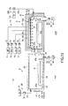
FIG. 10 is a sectional view showing part of the processing system according to the first embodiment of the present invention, which corresponds to the PHT processing apparatus and COR processing apparatus;
FIG. 11 is a sectional view showing part of a processing system according to a second embodiment of the present invention, which corresponds to a PHT processing apparatus and a COR processing apparatus;
FIG. 12 is a sectional view showing part of a processing system according to one example of a third embodiment of the present invention, which corresponds to a PHT processing apparatus and a COR processing apparatus; and
FIG. 13 is a sectional view showing part of a processing system according to an alternative example of the third embodiment of the present invention, which corresponds to a PHT processing apparatus and a COR processing apparatus.
DETAILED DESCRIPTION OF THE INVENTION
Embodiments of the present invention will now be described with reference to the accompanying drawings.
(First Embodiment)
FIG. 1 is a plan view schematically showing the structure of a processing system according to a first embodiment of the present invention. This processing system 1 a includes a load/unload section for loading and unloading semiconductor wafers (which may be simply referred to as “wafer” hereinafter) W to and from the processing system 1 a. Two load lock chambers (L/L) 3 are disposed adjacent to the load/unload section 2. PHT processing apparatuses (PHT) 4 are respectively disposed adjacent to the load lock chambers 3 and each configured to perform a PHT (Post Heat Treatment) process on a wafer W. COR processing apparatuses (COR) 5 are respectively disposed adjacent to the PHT processing apparatuses 4 and each configured to perform a COR process on a wafer W. The load lock chambers 3, PHT processing apparatuses 4, and COR processing apparatuses 5 are arrayed in rows in this order.
The load/unload section 2 includes a transfer chamber (L/M) 12 provided with a first wafer transfer mechanism 11 disposed therein to transfer wafers W. The first wafer transfer mechanism 11 includes two transfer arms 11 a and 11 b each for supporting a wafer W essentially in a horizontal state. A table 13 is disposed along the longitudinal side of the transfer chamber 12 and is provided with, e.g., three carriers C each of which can store a plurality of wafers W in an arrayed state. An orienter 14 is disposed adjacent to the transfer chamber 12 and configured to optically detect misalignment of a wafer W by rotating the wafer W and to perform alignment of the wafer W.
In the load/unload section 2, wafers W are supported by the transfer arms 11 a and 11 b, and are transferred to predetermined positions by the first wafer transfer mechanism 11 being moved linearly in a horizontal direction and a vertical direction. Further, wafers W are loaded and unloaded to and from the carriers C on the table 13, the orienter 14, and the load lock chambers 3 by the transfer arms 11 a and 11 b being moved back and forth.
The load lock chambers 3 are connected to the transfer chamber 12 respectively through gate valves 16 interposed therebetween. Each of the load lock chambers 3 is provided with a second wafer transfer mechanism 17 disposed therein to transfer wafers W. Each of the load lock chambers 3 is configured to be vacuum-exhausted to a predetermined vacuum level.
As shown in FIG. 2, the second wafer transfer mechanism 17 has an articulated structure with a transfer arm 17 a configured to support a wafer W essentially in a horizontal state. According to the wafer transfer mechanism 17, when the articulated structure is contracted, the transfer arm 17 a is positioned inside the load lock chamber 3. When the articulated structure is extended, the transfer arm 17 a is positioned inside the PHT processing apparatus 4. When the articulated structure is further extended, the transfer arm 17 a is positioned inside the COR processing apparatus 5. Accordingly, when a wafer W is supported on the transfer arm 17 a and the articulated structure of the second wafer transfer mechanism 17 is extended and/or contracted, the wafer W is transferred among the load lock chamber 3, PHT processing apparatus 4, and COR processing apparatus 5.
As shown in FIG. 3, each of the PHT processing apparatuses 4 includes a chamber 20 that is configured to be vacuum-exhausted and is provided with a table 23 disposed therein to support a wafer W. A heater 24 is embedded in the table 23 to heat a wafer W treated by the COR process, so as to perform a PHT process for evaporating (subliming) a reaction product generated by the COR process. The chamber 20 has a transfer port 20 a on the load lock chamber 3 side to transfer a wafer therethrough between the chamber 20 and load lock chamber 3. The transfer port 20 a is configured to be opened and closed by a gate valve 22. The chamber 20 further has a transfer port 20 b on the COR processing apparatus 5 side to transfer a wafer therethrough between the chamber 20 and COR processing apparatus 5. The transfer port 20 b is configured to be opened and closed by a gate valve 54. The chamber 20 is connected to an inactive gas supply mechanism 26 including a gas supply passage 25 for supplying an inactive gas, such as nitrogen gas (N2), and a reactive gas supply mechanism 28 including a gas supply passage 27 for supplying a gas, such as ammonia gas (NH3), which reacts with, e.g., fluorine (F). The chamber 20 is further connected to an exhaust mechanism 30 including an exhaust passage 29 for exhausting gas from inside the chamber 20. The inactive gas supply passage 25 is connected to a nitrogen gas supply source 31. The inactive gas supply passage 25 is provided with a flow rate regulation valve 32 configured to open and close the passage and to adjust the supply flow rate of nitrogen gas. The reactive gas supply passage 27 is connected to an ammonia gas supply source 34. The reactive gas supply passage 27 is provided with a flow rate regulation valve 33 configured to open and close the passage and to adjust the supply flow rate of NH3 gas. The exhaust passage 29 of the exhaust mechanism 30 is provided with a switching valve 35 and a vacuum pump 36.
As shown in FIGS. 4 and 5, each of the COR processing apparatuses 5 includes an airtight chamber 40 provided with a table 42 disposed therein to support a wafer W essentially in a horizontal state. The COR processing apparatus 5 includes a gas supply mechanism 43 for supplying HF gas, NH3 gas, and so forth into the chamber 40, and an exhaust mechanism 44 for exhausting gas from inside the chamber 40. When HF gas and NH3 gas are supplied into the chamber 40 while the pressure of the chamber 40 is maintained at a predetermined value, these gases come into contact with a wafer W and act on an oxide film (SiO2) formed on the wafer W, so that ammonium fluorosilicate ((NH4)2SiF6) is generated as a reaction product. The oxide film to be processed may be a natural oxide film formed on the surface of the wafer W or an oxide film used as a component of devices.
The chamber 40 is formed of a chamber main body 51 and a lid 52. The chamber main body 51 includes a bottom portion 51 a and an essentially cylindrical sidewall portion 51 b. The bottom of the sidewall portion 51 b is closed by the bottom portion 51 a and the top of the sidewall portion 51 b is formed as an opening. The lid 52 is attached to close this top opening. The lid 52 is airtightly attached to the sidewall portion 51 b with a seal member (not shown) interposed therebetween to ensure that the interior of the chamber 40 is kept airtight.
As shown in FIG. 5, a transfer port 53 is formed in the sidewall portion 51 b to transfer a wafer therethrough to and from the chamber 20 of the PHT processing apparatus 4. The transfer port 53 is configured to be opened and closed by a gate valve 54. Accordingly, the chamber 40 is connected through the gate valve 54 to the chamber 20 of the PHT processing apparatus 4.
The lid 52 includes a lid main body 52 a and a showerhead 52 b for delivering a process gas. The showerhead 52 b is disposed at the bottom of the lid main body 52 a, so that the bottom of the showerhead 52 b serves as the inner surface (the bottom) of the lid 52. The showerhead 52 b forms the ceiling of the chamber 40 above the table 42 to supply various gases from above onto a wafer W placed on the table 42. The showerhead 52 b has a plurality of delivery ports 52 c distributed all over the bottom thereof for delivering a gas.
The table 42 is essentially circular in the plan view and is fixed on the bottom portion 51 a. The table 42 is provided with a temperature adjusting member 55 disposed therein to adjust the temperature of the table 42. For example, the temperature adjusting member 55 comprises a conduit for circulating a temperature adjusting medium (such as water), so that the temperature of the table 42 can be adjusted by heat exchange with the temperature adjusting medium flowing through the conduit, and the temperature of the wafer W placed on the table 42 is thereby controlled.
The gas supply mechanism 43 includes the showerhead 52 b, an HF gas supply passage 61 for supplying HF gas into the chamber 40, an NH3 gas supply passage 62 for supplying NH3 gas, an Ar gas supply passage 63 for supplying Ar as an inactive gas, and an N2 gas supply passage 64 for supplying N2 gas. The HF gas supply passage 61, NH3 gas supply passage 62, Ar gas supply passage 63, and N2 gas supply passage 64 are connected to the showerhead 52 b, so that HF gas, NH3 gas, Ar gas, and N2 gas can be delivered through the showerhead 52 b into the chamber 40.
The HF gas supply passage 61 is connected to an HF gas supply source 71. The HF gas supply passage 61 is provided with a flow rate regulation valve 72 configured to open and close the passage and to adjust the supply flow rate of HF gas. Similarly, the NH3 gas supply passage 62 is connected to an NH3 gas supply source 73. The NH3 gas supply passage 62 is provided with a flow rate regulation valve 74 configured to open and close the passage and to adjust the supply flow rate of ammonia gas. The Ar gas supply passage 63 is connected to an Ar gas supply source 75. The Ar gas supply passage 63 is provided with a flow rate regulation valve 76 configured to open and close the passage and to adjust the supply flow rate of Ar gas. The N2 gas supply passage 64 is connected to an N2 gas supply source 77. The N2 gas supply passage 64 is provided with a flow rate regulation valve 78 configured to open and close the passage and to adjust the supply flow rate of nitrogen gas.
The exhaust mechanism 44 includes an exhaust passage 85 provided with a switching valve 82 and a vacuum pump 83 for performing forcible exhaust. One end of the exhaust passage 85 is connected to a hole formed in the bottom portion 51 a of the chamber 40.
Some of the components of the COR processing apparatus 5, such as the chamber 40 and table 42, are made of Al. The Al material of the chamber 40 may be bare Al or Al having an inner surface prepared by anodic oxidation (which corresponds to the inner surface of the chamber main body 51 and the bottom surface of the showerhead 52 b). On the other hand, since the Al surface of the table 42 is required to have high wear resistance, the surface is preferably prepared by anodic oxidation to form an oxide coating (Al2O3), which has high wear resistance.
As shown in FIG. 1, the processing system 1 a includes a control section 90. As shown in FIG. 6, the control section 90 includes a process controller 91 comprising a microprocessor (computer) for controlling the respective components of the processing system 1 a. The process controller 91 is connected to a user interface 92, which includes, e.g., a keyboard and a display, wherein the keyboard is used for an operator to input commands for operating the processing system 1 a, and the display is used for showing visualized images of the operational status of the processing system 1 a. The process controller 91 is further connected to a storage portion 93, which stores recipes i.e., control programs and various databases for the process controller 91 to control the processing system la so as to perform various processes including, e.g., process gas supply and gas exhaust for the chamber 40 in the COR processing apparatus 5, and for the respective components of the processing system 1 a to perform predetermined processes in accordance with process conditions. The recipes are stored in the storage medium of the storage portion 93. The storage medium may be of the stationary type, such as a hard disk, or of the portable type, such as a CD-ROM, DVD, or flash memory. Alternatively, the recipes may be used online while they are transmitted from another apparatus through, e.g., a dedicated line, as needed.
A required recipe is retrieved from the storage portion 93 and executed by the process controller 91 in accordance with an instruction or the like input through the user interface 92. Consequently, the processing system 1 a can perform a predetermined process under the control of the process controller 91.
Particularly, according to this embodiment, under the control of the process controller 91, a gas process is performed in the COR processing apparatus 5 and then a heating process is performed by use of an atmosphere of an inactive gas, such as N2 gas, in the PHT processing apparatus 4. Further, after this heating process, a gas process is continuously performed by use of an atmosphere of a gas, such as NH3 gas, which reacts with fluorine. Accordingly, the process controller 91 is preset to control the gas supply mechanisms 26 and 28 to supply the inactive gas into the chamber 20 and then supply the reactive gas into the chamber 20.
Next, an explanation will be given of such process operations of the processing system 1 a.
At first, the structure of a wafer W to be processed by the processing system 1 a will be explained.
FIG. 7A is a sectional view showing a main portion near the surface (device formation surface) of a wafer W. The wafer W comprises a semiconductor substrate 301, such as a silicon substrate 301. The substrate 301 is provided with source/drain regions 302 formed in the surface and having a conductivity type opposite to that of the substrate 301. The source/drain regions 302 are present with a channel region 303 interposed therebetween, on which a gate insulating film 304 consisting of a thermal oxide film (SiO2) is formed by thermally oxidizing the substrate 301. A gate electrode consisting of a conductive poly-silicon film 305 is formed on the gate insulating film 304. A cap layer 306 made of, e.g., silicon nitride (Si3N4) is formed on the conductive poly-silicon film 305. Sidewall insulating films 307 made of, e.g., silicon nitride (Si3N4) are formed on the sidewalls of the conductive poly-silicon film 305 and cap layer 306. The gate insulating film 304, conductive poly-silicon film 305, cap layer 306, and sidewall insulating films 307 constitute a gate electrode structure 308. The substrate 301 with the gate electrode structure 308 disposed thereon is covered with an inter-level insulating film 309 made of a low dielectric constant insulating material, such as SOD (Spin On Dielectric).
As shown in FIG. 7B, a contact hole 310 is formed in the inter-level insulating film 309 of the structure shown in FIG. 7A. The contact hole 310 formed in the inter-level insulating film 309 reaches the corresponding one of the source/drain regions 302. As shown in FIG. 7B, the contact hole 310 is formed by self alignment relative to the sidewall insulating films 307 by use of the difference between the etching rate of the inter-level insulating film 309 and the etching rate of the sidewall insulating films 307, which is made of silicon nitride different from the material of the inter-level insulating film 309. After the etching of the inter-level insulating film 309 is finished, a surface portion of the substrate 301 at the bottom of the contact hole 310, i.e., the surface of the source/drain region 302, is exposed and comes into contact with oxygen, and so a natural oxide film (SiO2) 311 is formed. The processing system 1 a described above can be utilized to remove this natural oxide film 311, for example.
Specifically, wafers W having the state shown in FIG. 7B are stored in a carrier C and are transferred to the processing system 1 a. In the processing system 1 a, the atmospheric side gate valve 16 of one of the load lock chambers 3 is opened, and a wafer W is transferred by one of the transfer arms 11 a and 11 b of the first wafer transfer mechanism 11 from the carrier C placed on the load/unload section 2 into this load lock chamber 3. In the load lock chamber 3, the wafer W is transferred from the transfer arm 11 a or 11 b onto the wafer transfer arm 17 a of the second wafer transfer mechanism 17 of the load lock chamber 3.
Then, the atmospheric side gate valve 16 is closed, and the interior of the load lock chambers 3 is vacuum-exhausted. Then, the gate valves 22 and 54 are opened, and the wafer transfer arm 17 a is extended into the COR processing apparatus 5 and places the wafer W onto the table 42.
Then, the transfer arm 17 a is returned back into the load lock chambers 3, and the gate valve 54 is closed to make the interior of the chamber 40 airtight. Then, NH3 gas, Ar gas, and N2 gas are supplied from the gas supply mechanism 43 into the chamber 40. Further, the temperature of the wafer W is adjusted by the temperature adjusting member 55 to a predetermined target value (for example, about 25° C.)
Then, HF gas is supplied from the gas supply mechanism 43 into the chamber 40. When HF gas is supplied into the chamber 40 with NH3 gas supplied in advance, an atmosphere containing HF gas and NH3 gas is formed inside the chamber 40, and starts a COR process on the wafer W. Consequently, the natural oxide film 311 present on the surface of the wafer W inside the contact hole 310 chemically reacts with molecules of the hydrogen fluoride gas and molecules of the ammonia gas, and so it is transformed into a reaction product 312, as shown in FIG. 7C. During the COR process, the interior of the chamber 40 is maintained at a predetermined pressure, such as about 13.3 Pa (0.1 Torr).
As the reaction product 312, ammonium fluorosilicate ((NH4)2SiF6), water, and so forth are generated.
After this process is finished, the gate valves 22 and 54 are opened, and the processed wafer W is transferred by the transfer arm 17 a of the second wafer transfer mechanism 17 from the table 42 onto the table 23 inside the chamber 20 of the PHT processing apparatus 4. Then, the transfer arm 17 a is returned back into the load lock chambers 3, and the gate valves 22 and 54 are closed. Then, while N2 gas is supplied into the chamber 20, the wafer W on table 23 is heated by the heater 24. The reaction product 312 generated by the COR process is evaporated by this heating and removed from the bottom of the contact hole 310. Consequently, this portion of the substrate 301, i.e., the surface of the source/drain region 302 in this embodiment, is exposed, as shown in FIG. 7D.
As described above, where the PHT process is performed after the COR process, the natural oxide film 311 is removed within a dry atmosphere, so that no water marks or the like are generated. Further, the natural oxide film 311 is removed by a plasma-less process, the wafer W is prevented from being damaged. Since the COR process stops making progress of etching when a predetermined time has elapsed, end point control thereof is unnecessary because no reaction is developed even if over-etching is preset.
However, as shown in FIG. 7E, after the PHT process is finished, fluorine and/or fluorine compound (such as CF), which are decomposition products of ammonium fluorosilicate ((NH4)2SiF6), may be left as residues 313 inside the contact hole 310. The residues 313 contain a halogen, such as fluorine in this example. If the wafer W with such residues 313 left thereon is exposed to the atmospheric air, the residues 313 may involve components, such as moisture (H2O), contained in the atmospheric air, and cause abnormal reactions with some components of the integrated circuit, such as the substrate 301, gate electrode (poly-silicon film 305), sidewall insulating films 307, inter-level insulating film 309, and interconnection layers formed later. FIGS. 9A and 9B show comparative examples where abnormal reactions are caused.
As shown in FIG. 9A, if the wafer W with the residues 313 left thereon is exposed to the atmospheric air, components (such as H2O) contained in the atmospheric air, a halogen contained in the residues 313, and structural components (such as Si, SiO2, and Si3N4), on which the residues 313 are deposited, react with each other and bring about a reaction product 314 grown larger. Further, if the reaction product 314 is kept exposed to the atmospheric air, the product 314 may be transformed into a different foreign substance. When an interconnection layer 315 is formed in the contact hole 310 with the reaction product 314 and/or foreign substance left therein, the semiconductor integrated circuit device is adversely affected such that the interconnection layer 315 is thinner, as shown in FIG. 9B, for example. Even if the interconnection layer 315 is thinner, the electric connection between the interconnection layer 315 and source/drain region 302 is not completely cut off, but allows the semiconductor integrated circuit device to operate. However, semiconductor integrated circuit devices formed on the same wafer may largely differ from each other in characteristic, and/or this semiconductor integrated circuit device may suffer a difficulty in operating at a high speed. Further, the reaction product 314 and/or foreign substance may be grown to a size that clogs the entrance of the contact hole 310. Alternatively, with an increase in the miniaturization level in the future, the contact hole 310 may become smaller so that it can be easily clogged with the reaction product 314 and/or foreign substance even if they are small. Such clogging may deteriorate the yield of semiconductor integrated circuit devices.
In light of residues 313 that can be generated after the PHT process, this embodiment is arranged to remove such residues 313, even if the residues 313 are generated by any chance.
Specifically, after the wafer W is subjected to the gas process, i.e., the COR process in this embodiment, the wafer W is subjected to a heating process, i.e., the PHT process in this embodiment, while the wafer W is subjected to a gas process within an atmosphere containing a reactive gas that reacts with fluorine. Alternatively, after the wafer W is subjected to the PHT process, the wafer W is subjected to a gas process within an atmosphere containing a reactive gas that reacts with fluorine. In this way, the wafer W is subjected to a gas process to prevent residues 313 from being generated or to remove residues 313 even if they are generated.
For example, in order to remove residues 313 possibly generated, this embodiment is arranged to supply N2 gas into the chamber 20 while heating the wafer W on the table 23 by the heater 24, and then, as it is, to supply a gas that reacts with fluorine into the chamber 20 without opening the gate valves 22 and 54.
In this embodiment, as shown FIG. 7D, the wafer W is heated within an N2 gas atmosphere, so that the reaction product 312 and moisture, which has been generated in the process of transformation of the natural oxide film 311 into the reaction product 312, are sufficiently evaporated from the wafer W. After these substances are sufficiently removed, as shown in FIG. 7F, a gas, such as NH3 gas in this embodiment, which reacts with fluorine is supplied into the chamber 20 in addition to N2 gas, so that residues 313 containing fluorine and/or fluorine compound are removed. Particularly, where NH3 gas is used as a gas that reacts with fluorine, the wafer W is preferably treated by the PHT process to sufficiently evaporate moisture (H2O) during the PHT process, before the residues 313 are removed, i.e., before the wafer W is subjected to a gas process within an atmosphere containing NH3 gas. This is so, because NH3 gas can easily react with H2O and produce ammonia water, although by a slight amount, that dissolves structural components on the wafer W. Where NH3 gas is used to remove the residues 313, moisture should be sufficiently evaporated to suppress undesirable etching of structural components on the wafer W. In order to sufficiently evaporate moisture, as shown in FIG. 7D, a heating process is preferably performed within an atmosphere of an inactive gas, such as N2 gas, before a gas that reacts with fluorine is supplied into the chamber 20.
Further, the step shown in FIG. 7F should be performed under conditions that allow the residues 313 to be sufficiently removed, even if the residues 313, which contain fluorine and/or fluorine compound, are present by any chance. In light of this, this step is preferably performed while the wafer W is being heated to promote a reaction for removing the residues 313. For example, the wafer W is set at a temperature of 100 to 200° C. The process pressure is preferably set at a low pressure to promote evaporation of the residues 313. For example, the process pressure is set to be 500 to 1,000 mTorr.
A series of processes shown in FIGS. 7C to 7F performed in the processing system 1 a may be stored as a recipe in the storage medium of the storage portion 93 of the control section 90. Where such a recipe is stored in the storage medium, it can be executed under the control of the process controller 91. As shown in FIG. 7F, where the residue removal process is performed continuously to the PHT process, the residues 313 can be removed even if the residues 313 are present by any chance. Consequently, it is possible to decrease the probability of abnormal reactions being caused in semiconductor integrated circuit devices and thereby maintain and improve the characteristic and yield of the semiconductor integrated circuit devices.
After the residue removal process is finished, the wafer W is transferred by the transfer arm 17 a of the second wafer transfer mechanism 17 into the load lock chamber 3. Then, the gate valve 22 is closed, the interior of the load lock chambers 3 is returned to atmospheric pressure, and the wafer W is inserted by the first wafer transfer mechanism 11 into a carrier C placed in the load/unload section 2.
The operations described above are repeated the necessary times corresponding to the number of wafers W stored in a carrier C, so that the processes on the wafers W are finished. Thereafter, as shown in FIG. 8, other processes for manufacturing semiconductor integrated circuit devices are continuously performed, such that, e.g., an interconnection layer 315 is formed in the contact hole 310.
As described above, according to the first embodiment, residues containing fluorine and/or fluorine compound are removed, so that the probability of abnormal reactions being caused is lowered. Consequently, there is provided a processing system (substrate processing system) and substrate processing method that can maintain and improve the characteristic and yield of semiconductor integrated circuit devices. Further, there is provided a computer readable storage medium that stores a recipe (program) for controlling the processing system (substrate processing system) in accordance with the substrate processing method.
Further, according to the first embodiment, as shown in FIG. 10, the processing system 1 a is arranged such that a natural oxide film formed on the surface of a target substrate, such as a wafer W, is transformed into a reaction product inside the vacuum chamber 40 of the COR processing apparatus 5. Thereafter, without being exposed to the atmospheric air, the wafer W with the reaction product thus formed is transferred through the gate valve 54 into the vacuum chamber 20 of the PHT processing apparatus 4. Then, inside the chamber 20, the reaction product is evaporated, and the residues 313 containing fluorine and/or fluorine compound are removed from the wafer W. In other words, the first embodiment is arranged to remove the residues 313 without exposing the target substrate to the atmospheric air. Consequently, as compared to a case where a target substrate is exposed to the atmospheric air and transferred to another processing system to remove the residues 313, this embodiment make it possible to remove the residues 313 while decreasing the probability of abnormal growth of the residues 313 or the probability of re-contamination inside the load/unload section 2 or a carrier C due to the wafer W transferred therein along with the residues 313 deposited thereon. Consequently, the residues 313 can be reliably removed while the target substrate is maintained in a clean state. Such removal of the residues 313 is effectively applied to semiconductor integrated circuit devices manufactured in accordance with higher levels of miniaturization and integration.
In addition, according to the first embodiment, evaporation of the reaction product 312 and removal of the residues 313 are continuously performed in this order inside the vacuum chamber 20 of the PHT processing apparatus 4. Consequently, it is possible to enhance the effect described above in that the residues 313 are reliably removed while the target substrate is maintained in a clean state.
(Second Embodiment)
FIG. 11 is a sectional view showing part of a processing system 1 b according to a second embodiment of the present invention, which corresponds to a PHT processing apparatus 4 and a COR processing apparatus 5.
As shown in FIG. 10, the first embodiment is arranged to supply a gas, such as NH3 gas, which reacts with fluorine into the chamber 20 of the PHT processing apparatus 4.
However, the chamber 40 of the COR processing apparatus 5 is originally provided with a supply passage for supplying NH3 gas. This facility can be used to perform a process for removing the residues 313.
As shown in FIG. 11, the processing system 1 b according to the second embodiment differs from the processing system 1 a according to the first embodiment, such that the chamber 20 of the PHT processing apparatus 4 is not provided with a supply passage for supplying a gas, such as NH3 gas, which reacts with fluorine.
The processing system 1 b according to the second embodiment is arranged to perform a process for removing the residues 313, as follows.
At first, a wafer W is transferred into the chamber 40 through the gate valves 22 and 54 and chamber 20. Then, the gate valve 54 is closed, and the COR process (a process for transforming a natural oxide film into a reaction product) is performed inside the chamber 40.
Then, the wafer W is transferred through the gate valve 54 from the chamber 40 into the chamber 20. Then, the gate valves 22 and 54 are closed, and the PHT process (a process for evaporating the reaction product) is performed inside the chamber 20.
Then, the wafer W is transferred through the gate valve 54 from the chamber 20 into the chamber 40. Then, the gate valve 54 is closed, and a process for removing the residues 313 is performed inside the chamber 40.
For example, these COR process, PHT process, and process for removing the residues 313 are performed under the same conditions as those of the first embodiment.
In the processing system 1 b according to the second embodiment, the COR process and process for removing the residues 313 are performed inside the chamber 40. The process for removing the residues 313 is a heating process. Accordingly, the table 42 may be preferably provided with a heater disposed therein for heating the wafer W in addition to the temperature adjusting member 55 for adjusting the temperature of the wafer W. Alternatively, the temperature adjusting member 55 may be preferably arranged to have a heating function in addition to the temperature adjust function.
The processing system 1 b according to the second embodiment can also have the effect of removing the residues 313, as in the first embodiment. Further, the chamber 20 of the PHT processing apparatus 4 does not have to be provided with a supply passage for supplying a gas, such as NH3 gas, which reacts with fluorine, and so the structure of the processing system 1 b can be preferably simplified.
(Third Embodiment)
After the residues 313 are removed, a gas process may be performed on the surface of a target substrate, such as a wafer W, by supplying a reducing gas (such as, H2, CH2, or NH3), so as to apply hydrogen termination to the surface of the wafer W treated by the residue removal.
Particularly, where a natural oxide film is removed from the surface of the silicon substrate 301 of a wafer W, hydrogen can be easily attached to silicon dangling bonds (disconnected bonds) exposed on the substrate surface. Consequently, the surface of the substrate 301 becomes inactive and easily generates traps, which make it difficult to manufacture semiconductor integrated circuit devices of high quality.
For example, a processing system for this purpose is arranged as shown in FIG. 12. Specifically, the chamber 20 is provided with a hydrogen (H2) gas supply mechanism 104 including a gas supply passage 103 for supplying hydrogen gas into the chamber 20 from a hydrogen gas supply source 101 through a flow rate regulation valve 102.
The processing system 1 c according to this example can supply H2 gas into the chamber 20 of the PHT processing apparatus 4, and so this system is suitably applied to a case where a process for removing the residues 313 is performed inside the chamber 20. After the process for removing the residues 313 is performed, the hydrogen termination process is performed inside the same chamber 20, so that hydrogen termination is applied to the surface of the wafer W, particularly, the surface of the silicon substrate 301, before other substances are attached to dangling bonds on the surface. Consequently, the hydrogen termination can be efficiently performed on the surface of the silicon substrate 301.
As an alternative example, as shown in FIG. 13, the hydrogen gas supply mechanism 104 shown in FIG. 12 may be connected to the chamber 40 of the COR processing apparatus 5.
The processing system 1 d according to this alternative example can supply H2 gas into the chamber 40 of the COR processing apparatus 5, and so this system is suitably applied to a case where a process for removing the residues 313 is performed inside the chamber 40.
As described above, according to the third embodiment, after the process for removing the residues 313 is performed, the hydrogen termination process is further performed on the wafer W in the same chamber, for example. Where the cleaned surface of the wafer W, from which the residues 313 have been removed, is further subjected to the hydrogen termination in the same chamber, semiconductor integrated circuit devices of high quality can be more reliably manufactured.
(Fourth Embodiment)
In the first to third embodiments, a gas process is performed on a wafer W within an atmosphere of a mixture of HF gas and NH3 gas, so that a natural oxide film is transformed into a reaction product. However, a method for transforming a natural oxide film into a reaction product is not limited to this method. For example, as a gas containing fluorine, NF3 gas may be used in place of HF gas.
Where NF3 gas is used, a chamber including a plasma generating section is used, for example, and N2 gas and H2 gas are supplied into the plasma generating section to generate plasma of N2 gas and H2 gas. Then, while the plasma of N2 gas and H2 gas (i.e., radicals) is supplied onto a wafer W, NF3 gas is added into the flow of the plasma.
According to these embodiments of the present invention, there is provided a substrate processing method and substrate processing system that can decrease the probability of abnormal reactions being caused and thereby maintain and improve the characteristic and yield of semiconductor integrated circuit devices. Further, there is provided a computer readable storage medium that stores a program for controlling the substrate processing system.
The present invention has been described with reference to first to fourth embodiments, but the present invention is not limited to the embodiments described above, and it may be modified in various manners.
For example, the embodiments described above are explained in a case where a natural oxide film is removed from the bottom of a contact hole formed on a wafer W. However, the preset invention is applicable to any process for removing a natural oxide film other than a process for removing a natural oxide film from the bottom of a contact hole.
In place of removal of a natural oxide film, the preset invention may be applied to another process used for manufacturing semiconductor integrated circuit devices, where a gas process is performed by use of a fluorine-containing process gas to form a fluorine-containing reaction product, and then a process is preformed to decompose the reaction product. Also in this case, it is possible to provide the effect of removing residues containing fluorine and/or fluorine compound.
In the embodiments described above, the PHT processing apparatus 4 and COR processing apparatus 5 include their own N2 gas supply source and NH3 gas supply source. However, the PHT processing apparatus 4 and COR processing apparatus 5 may include their own gas supply sources or share common gas supply sources.
In the embodiments described above, NH3 is used as a gas that can easily react with fluorine, but another gas, such as CO or NO, may be alternatively used.
Additional advantages and modifications will readily occur to those skilled in the art. Therefore, the invention in its broader aspects is not limited to the specific details and representative embodiments shown and described herein. Accordingly, various modifications may be made without departing from the spirit or scope of the general inventive concept as defined by the appended claims and their equivalents.

Claims (19)

What is claimed is:
1. A substrate processing system comprising:
a first gas supply section configured to supply a fluorine-containing gas to a process object;
a second gas supply section configured to supply a reactive gas that reacts with fluorine to the process object; and
a control section configured to control operation of the system,
wherein the control section includes a computer readable non-transitory storage medium that stores a control program for execution on a computer, the control program, when executed, causing the control section to control the system to conduct a process sequence for processing a target substrate as the process object, the process sequence including:
performing a first gas process of processing the target substrate within an atmosphere containing the fluorine-containing gas supplied from the first gas supply section to form a reaction product containing fluorine on a surface of the target substrate;
performing a heating process to evaporate the reaction product containing fluorine from the surface of the target substrate; and
performing a second gas process of processing the target substrate within an atmosphere containing the reactive gas supplied from the second gas supply section to prevent residues of the reaction product containing fluorine from being generated or to remove the residues if they are generated.
2. The system according to claim 1, wherein the system further comprises a heating mechanism configured to heat the process object.
3. The system according to claim 2, wherein the second gas process is performed while heating the target substrate by the heating mechanism.
4. The system according to claim 2, wherein the heating process to evaporate the reaction product containing fluorine from the surface of the target substrate is performed without supplying either of the fluorine-containing gas and the reactive gas to the target substrate.
5. The system according to claim 1, wherein the residues contain at least one of fluorine and a fluorine compound, the residues being on the surface of the target substrate.
6. The system according to claim 5, wherein the target substrate includes a contact hole formed therein for forming an interconnection, the first gas process includes forming the reaction product inside the contact hole, and the second gas process includes removing the residues remaining inside the contact hole.
7. The system according to claim 6, wherein the first gas supply section is configured further to supply NH3 gas to the process object, and the first gas process includes transforming a natural oxide film present inside the contact hole into the reaction product by causing the fluorine-containing gas and the NH3 gas supplied from the first gas supply section to chemically react with the natural oxide film.
8. The system according to claim 7, wherein the reactive gas is NH3 gas, and the performing the heating process further includes evaporating moisture generated on the target substrate in transformation of the natural oxide film into the reaction product.
9. The system according to claim 8, wherein the heating process includes heating the target substrate within an inactive gas atmosphere without supplying either of the fluorine-containing gas and the reactive gas to the target substrate.
10. The system according to claim 1, wherein the reactive gas is selected from the group consisting of NH3, CO, and NO.
11. The system according to claim 1, wherein the fluorine-containing gas is selected from the group consisting of HF and NF3 .
12. The system according to claim 11, wherein the first gas process includes transforming a natural oxide film into the reaction product.
13. The system according to claim 1, wherein, after the second gas process, the process sequence further includes performing a third gas process of processing the target substrate within an atmosphere containing a reducing gas to apply hydrogen termination to the surface of the target substrate.
14. The system according to claim 1, wherein the reactive gas is NH3 gas, and the performing the heating process further includes, evaporating moisture on the target substrate.
15. The system according to claim 14, wherein the heating process includes heating the target substrate within an inactive gas atmosphere without supplying either of the fluorine-containing gas and the reactive gas to the target substrate.
16. The system according to claim 1, wherein the first gas supply section is provided to a first process chamber equipped with an inactive gas supply section and an exhaust mechanism, the second gas supply section is provided to a second process chamber equipped with an inactive gas supply section and an exhaust mechanism, and the first and second process chambers are connected to each other by a gate valve.
17. The system according to claim 16, wherein a load lock chamber is connected to the second process chamber through a gate valve on a side opposite to the first process chamber, and a transfer arm is disposed inside the load lock chamber and configured to transfer the process object to and from the first and second process chambers.
18. The system according to claim 16, wherein the second process chamber further includes a gas supply section configured to supply H2 gas to apply hydrogen termination to a surface of the process object.
19. The system according to claim 1, wherein the first and second gas supply sections are provided to a process chamber equipped with an inactive gas supply section and an exhaust mechanism.
US13/292,518 2007-12-27 2011-11-09 Substrate processing method and system Expired - Fee Related US8991333B2 (en)

Priority Applications (1)

Application Number Priority Date Filing Date Title
US13/292,518 US8991333B2 (en) 2007-12-27 2011-11-09 Substrate processing method and system

Applications Claiming Priority (4)

Application Number Priority Date Filing Date Title
JP2007336521A JP5374039B2 (en) 2007-12-27 2007-12-27 Substrate processing method, substrate processing apparatus, and storage medium
JP2007-336521 2007-12-27
US12/314,933 US20090191340A1 (en) 2007-12-27 2008-12-18 Substrate processing method and system
US13/292,518 US8991333B2 (en) 2007-12-27 2011-11-09 Substrate processing method and system

Related Parent Applications (1)

Application Number Title Priority Date Filing Date
US12/314,933 Continuation US20090191340A1 (en) 2007-12-27 2008-12-18 Substrate processing method and system

Publications (2)

Publication Number Publication Date
US20120055401A1 US20120055401A1 (en) 2012-03-08
US8991333B2 true US8991333B2 (en) 2015-03-31

Family

ID=40899514

Family Applications (2)

Application Number Title Priority Date Filing Date
US12/314,933 Abandoned US20090191340A1 (en) 2007-12-27 2008-12-18 Substrate processing method and system
US13/292,518 Expired - Fee Related US8991333B2 (en) 2007-12-27 2011-11-09 Substrate processing method and system

Family Applications Before (1)

Application Number Title Priority Date Filing Date
US12/314,933 Abandoned US20090191340A1 (en) 2007-12-27 2008-12-18 Substrate processing method and system

Country Status (4)

Country Link
US (2) US20090191340A1 (en)
JP (1) JP5374039B2 (en)
KR (1) KR101553075B1 (en)
TW (1) TWI381432B (en)

Cited By (2)

* Cited by examiner, † Cited by third party
Publication number Priority date Publication date Assignee Title
US20140290752A1 (en) * 2013-03-28 2014-10-02 Tokyo Electron Limited Processing method and processing apparatus
US20220199440A1 (en) * 2020-12-17 2022-06-23 Samsung Electronics Co., Ltd. Apparatus for processing a substrate

Families Citing this family (187)

* Cited by examiner, † Cited by third party
Publication number Priority date Publication date Assignee Title
JP5374039B2 (en) * 2007-12-27 2013-12-25 東京エレクトロン株式会社 Substrate processing method, substrate processing apparatus, and storage medium
JP5629098B2 (en) * 2010-01-20 2014-11-19 東京エレクトロン株式会社 Pattern repair method on silicon substrate
WO2012063901A1 (en) * 2010-11-11 2012-05-18 東京エレクトロン株式会社 Device for producing and method for producing semiconductor device
US20130023129A1 (en) 2011-07-20 2013-01-24 Asm America, Inc. Pressure transmitter for a semiconductor processing environment
JP6110848B2 (en) * 2012-05-23 2017-04-05 東京エレクトロン株式会社 Gas processing method
US10115608B2 (en) * 2012-05-25 2018-10-30 Novellus Systems, Inc. Method and apparatus for rapid pump-down of a high-vacuum loadlock
JP5997555B2 (en) * 2012-09-14 2016-09-28 東京エレクトロン株式会社 Etching apparatus and etching method
US10295591B2 (en) * 2013-01-02 2019-05-21 Texas Instruments Incorporated Method and device for testing wafers
US20160376700A1 (en) 2013-02-01 2016-12-29 Asm Ip Holding B.V. System for treatment of deposition reactor
JP6258656B2 (en) * 2013-10-17 2018-01-10 東京エレクトロン株式会社 Substrate processing method and substrate processing apparatus
JP6405958B2 (en) 2013-12-26 2018-10-17 東京エレクトロン株式会社 Etching method, storage medium, and etching apparatus
JP6435667B2 (en) 2014-07-01 2018-12-12 東京エレクトロン株式会社 Etching method, etching apparatus and storage medium
JP6566430B2 (en) 2014-08-12 2019-08-28 東京エレクトロン株式会社 Substrate processing method
US10941490B2 (en) 2014-10-07 2021-03-09 Asm Ip Holding B.V. Multiple temperature range susceptor, assembly, reactor and system including the susceptor, and methods of using the same
US10276355B2 (en) 2015-03-12 2019-04-30 Asm Ip Holding B.V. Multi-zone reactor, system including the reactor, and method of using the same
CN106158640A (en) * 2015-04-03 2016-11-23 中芯国际集成电路制造(上海)有限公司 A kind of semiconductor device and preparation method thereof, electronic installation
JP6839096B2 (en) * 2015-04-29 2021-03-03 アプライド マテリアルズ インコーポレイテッドApplied Materials,Incorporated Methods and devices for correcting substrate deformation
US11139308B2 (en) 2015-12-29 2021-10-05 Asm Ip Holding B.V. Atomic layer deposition of III-V compounds to form V-NAND devices
JP6854611B2 (en) * 2016-01-13 2021-04-07 東京エレクトロン株式会社 Substrate processing method, substrate processing equipment and substrate processing system
US10529554B2 (en) 2016-02-19 2020-01-07 Asm Ip Holding B.V. Method for forming silicon nitride film selectively on sidewalls or flat surfaces of trenches
JP6601257B2 (en) 2016-02-19 2019-11-06 東京エレクトロン株式会社 Substrate processing method
KR101895557B1 (en) 2016-04-05 2018-09-06 주식회사 테스 Method for selective etching of silicon oxide film
US11453943B2 (en) 2016-05-25 2022-09-27 Asm Ip Holding B.V. Method for forming carbon-containing silicon/metal oxide or nitride film by ALD using silicon precursor and hydrocarbon precursor
US9859151B1 (en) 2016-07-08 2018-01-02 Asm Ip Holding B.V. Selective film deposition method to form air gaps
US10612137B2 (en) 2016-07-08 2020-04-07 Asm Ip Holdings B.V. Organic reactants for atomic layer deposition
US9887082B1 (en) 2016-07-28 2018-02-06 Asm Ip Holding B.V. Method and apparatus for filling a gap
US9812320B1 (en) 2016-07-28 2017-11-07 Asm Ip Holding B.V. Method and apparatus for filling a gap
US11532757B2 (en) 2016-10-27 2022-12-20 Asm Ip Holding B.V. Deposition of charge trapping layers
US10714350B2 (en) 2016-11-01 2020-07-14 ASM IP Holdings, B.V. Methods for forming a transition metal niobium nitride film on a substrate by atomic layer deposition and related semiconductor device structures
KR102546317B1 (en) 2016-11-15 2023-06-21 에이에스엠 아이피 홀딩 비.브이. Gas supply unit and substrate processing apparatus including the same
US11581186B2 (en) * 2016-12-15 2023-02-14 Asm Ip Holding B.V. Sequential infiltration synthesis apparatus
US11447861B2 (en) 2016-12-15 2022-09-20 Asm Ip Holding B.V. Sequential infiltration synthesis apparatus and a method of forming a patterned structure
US11390950B2 (en) 2017-01-10 2022-07-19 Asm Ip Holding B.V. Reactor system and method to reduce residue buildup during a film deposition process
US10468261B2 (en) 2017-02-15 2019-11-05 Asm Ip Holding B.V. Methods for forming a metallic film on a substrate by cyclical deposition and related semiconductor device structures
US10770286B2 (en) 2017-05-08 2020-09-08 Asm Ip Holdings B.V. Methods for selectively forming a silicon nitride film on a substrate and related semiconductor device structures
US11306395B2 (en) 2017-06-28 2022-04-19 Asm Ip Holding B.V. Methods for depositing a transition metal nitride film on a substrate by atomic layer deposition and related deposition apparatus
JP6796559B2 (en) * 2017-07-06 2020-12-09 東京エレクトロン株式会社 Etching method and residue removal method
KR20190009245A (en) 2017-07-18 2019-01-28 에이에스엠 아이피 홀딩 비.브이. Methods for forming a semiconductor device structure and related semiconductor device structures
US10590535B2 (en) 2017-07-26 2020-03-17 Asm Ip Holdings B.V. Chemical treatment, deposition and/or infiltration apparatus and method for using the same
US10692741B2 (en) 2017-08-08 2020-06-23 Asm Ip Holdings B.V. Radiation shield
US10770336B2 (en) 2017-08-08 2020-09-08 Asm Ip Holding B.V. Substrate lift mechanism and reactor including same
US11769682B2 (en) 2017-08-09 2023-09-26 Asm Ip Holding B.V. Storage apparatus for storing cassettes for substrates and processing apparatus equipped therewith
US11830730B2 (en) 2017-08-29 2023-11-28 Asm Ip Holding B.V. Layer forming method and apparatus
US11295980B2 (en) 2017-08-30 2022-04-05 Asm Ip Holding B.V. Methods for depositing a molybdenum metal film over a dielectric surface of a substrate by a cyclical deposition process and related semiconductor device structures
KR102003361B1 (en) 2017-09-19 2019-07-24 무진전자 주식회사 Method and apparatus for in-situ dry clean processing
KR101981738B1 (en) 2017-09-19 2019-05-27 무진전자 주식회사 Substrate processing method and apparatus
US10658205B2 (en) 2017-09-28 2020-05-19 Asm Ip Holdings B.V. Chemical dispensing apparatus and methods for dispensing a chemical to a reaction chamber
TWI791689B (en) 2017-11-27 2023-02-11 荷蘭商Asm智慧財產控股私人有限公司 Apparatus including a clean mini environment
JP7214724B2 (en) 2017-11-27 2023-01-30 エーエスエム アイピー ホールディング ビー.ブイ. Storage device for storing wafer cassettes used in batch furnaces
US10872771B2 (en) 2018-01-16 2020-12-22 Asm Ip Holding B. V. Method for depositing a material film on a substrate within a reaction chamber by a cyclical deposition process and related device structures
CN111630203A (en) 2018-01-19 2020-09-04 Asm Ip私人控股有限公司 Method for depositing gap filling layer by plasma auxiliary deposition
TW202325889A (en) 2018-01-19 2023-07-01 荷蘭商Asm 智慧財產控股公司 Deposition method
US11081345B2 (en) 2018-02-06 2021-08-03 Asm Ip Holding B.V. Method of post-deposition treatment for silicon oxide film
US10896820B2 (en) 2018-02-14 2021-01-19 Asm Ip Holding B.V. Method for depositing a ruthenium-containing film on a substrate by a cyclical deposition process
JP7124098B2 (en) 2018-02-14 2022-08-23 エーエスエム・アイピー・ホールディング・ベー・フェー Method for depositing a ruthenium-containing film on a substrate by a cyclical deposition process
KR102636427B1 (en) 2018-02-20 2024-02-13 에이에스엠 아이피 홀딩 비.브이. Substrate processing method and apparatus
US10975470B2 (en) 2018-02-23 2021-04-13 Asm Ip Holding B.V. Apparatus for detecting or monitoring for a chemical precursor in a high temperature environment
US11473195B2 (en) 2018-03-01 2022-10-18 Asm Ip Holding B.V. Semiconductor processing apparatus and a method for processing a substrate
KR102646467B1 (en) 2018-03-27 2024-03-11 에이에스엠 아이피 홀딩 비.브이. Method of forming an electrode on a substrate and a semiconductor device structure including an electrode
US11222794B2 (en) * 2018-03-30 2022-01-11 Taiwan Semiconductor Manufacturing Co., Ltd Semiconductor fabrication system embedded with effective baking module
KR102596988B1 (en) 2018-05-28 2023-10-31 에이에스엠 아이피 홀딩 비.브이. Method of processing a substrate and a device manufactured by the same
US11718913B2 (en) 2018-06-04 2023-08-08 Asm Ip Holding B.V. Gas distribution system and reactor system including same
US10797133B2 (en) 2018-06-21 2020-10-06 Asm Ip Holding B.V. Method for depositing a phosphorus doped silicon arsenide film and related semiconductor device structures
KR102568797B1 (en) 2018-06-21 2023-08-21 에이에스엠 아이피 홀딩 비.브이. Substrate processing system
CN112292478A (en) 2018-06-27 2021-01-29 Asm Ip私人控股有限公司 Cyclic deposition methods for forming metal-containing materials and films and structures containing metal-containing materials
WO2020003000A1 (en) 2018-06-27 2020-01-02 Asm Ip Holding B.V. Cyclic deposition methods for forming metal-containing material and films and structures including the metal-containing material
US10755922B2 (en) 2018-07-03 2020-08-25 Asm Ip Holding B.V. Method for depositing silicon-free carbon-containing film as gap-fill layer by pulse plasma-assisted deposition
US10388513B1 (en) 2018-07-03 2019-08-20 Asm Ip Holding B.V. Method for depositing silicon-free carbon-containing film as gap-fill layer by pulse plasma-assisted deposition
US11430674B2 (en) 2018-08-22 2022-08-30 Asm Ip Holding B.V. Sensor array, apparatus for dispensing a vapor phase reactant to a reaction chamber and related methods
KR102140722B1 (en) 2018-08-22 2020-08-04 무진전자 주식회사 Dry clean apparatus and method using atmospheric plasma and steam
US11024523B2 (en) 2018-09-11 2021-06-01 Asm Ip Holding B.V. Substrate processing apparatus and method
KR20200030162A (en) 2018-09-11 2020-03-20 에이에스엠 아이피 홀딩 비.브이. Method for deposition of a thin film
CN110970344A (en) 2018-10-01 2020-04-07 Asm Ip控股有限公司 Substrate holding apparatus, system including the same, and method of using the same
KR102592699B1 (en) 2018-10-08 2023-10-23 에이에스엠 아이피 홀딩 비.브이. Substrate support unit and apparatuses for depositing thin film and processing the substrate including the same
KR102546322B1 (en) 2018-10-19 2023-06-21 에이에스엠 아이피 홀딩 비.브이. Substrate processing apparatus and substrate processing method
US11087997B2 (en) 2018-10-31 2021-08-10 Asm Ip Holding B.V. Substrate processing apparatus for processing substrates
KR20200051105A (en) 2018-11-02 2020-05-13 에이에스엠 아이피 홀딩 비.브이. Substrate support unit and substrate processing apparatus including the same
US11572620B2 (en) 2018-11-06 2023-02-07 Asm Ip Holding B.V. Methods for selectively depositing an amorphous silicon film on a substrate
US10818758B2 (en) 2018-11-16 2020-10-27 Asm Ip Holding B.V. Methods for forming a metal silicate film on a substrate in a reaction chamber and related semiconductor device structures
JP7336873B2 (en) * 2018-11-30 2023-09-01 東京エレクトロン株式会社 Substrate processing method
CN111261514A (en) * 2018-11-30 2020-06-09 东京毅力科创株式会社 Substrate processing method
KR102636428B1 (en) 2018-12-04 2024-02-13 에이에스엠 아이피 홀딩 비.브이. A method for cleaning a substrate processing apparatus
US11158513B2 (en) 2018-12-13 2021-10-26 Asm Ip Holding B.V. Methods for forming a rhenium-containing film on a substrate by a cyclical deposition process and related semiconductor device structures
JP2020096183A (en) 2018-12-14 2020-06-18 エーエスエム・アイピー・ホールディング・ベー・フェー Method of forming device structure using selective deposition of gallium nitride, and system for the same
TWI819180B (en) 2019-01-17 2023-10-21 荷蘭商Asm 智慧財產控股公司 Methods of forming a transition metal containing film on a substrate by a cyclical deposition process
TW202104632A (en) 2019-02-20 2021-02-01 荷蘭商Asm Ip私人控股有限公司 Cyclical deposition method and apparatus for filling a recess formed within a substrate surface
KR20200102357A (en) 2019-02-20 2020-08-31 에이에스엠 아이피 홀딩 비.브이. Apparatus and methods for plug fill deposition in 3-d nand applications
TW202044325A (en) 2019-02-20 2020-12-01 荷蘭商Asm Ip私人控股有限公司 Method of filling a recess formed within a surface of a substrate, semiconductor structure formed according to the method, and semiconductor processing apparatus
TW202100794A (en) 2019-02-22 2021-01-01 荷蘭商Asm Ip私人控股有限公司 Substrate processing apparatus and method for processing substrate
US11742198B2 (en) 2019-03-08 2023-08-29 Asm Ip Holding B.V. Structure including SiOCN layer and method of forming same
KR20200108242A (en) 2019-03-08 2020-09-17 에이에스엠 아이피 홀딩 비.브이. Method for Selective Deposition of Silicon Nitride Layer and Structure Including Selectively-Deposited Silicon Nitride Layer
KR20200116033A (en) 2019-03-28 2020-10-08 에이에스엠 아이피 홀딩 비.브이. Door opener and substrate processing apparatus provided therewith
KR20200116855A (en) 2019-04-01 2020-10-13 에이에스엠 아이피 홀딩 비.브이. Method of manufacturing semiconductor device
KR20200123380A (en) 2019-04-19 2020-10-29 에이에스엠 아이피 홀딩 비.브이. Layer forming method and apparatus
KR20200125453A (en) 2019-04-24 2020-11-04 에이에스엠 아이피 홀딩 비.브이. Gas-phase reactor system and method of using same
KR20200130121A (en) 2019-05-07 2020-11-18 에이에스엠 아이피 홀딩 비.브이. Chemical source vessel with dip tube
KR20200130652A (en) 2019-05-10 2020-11-19 에이에스엠 아이피 홀딩 비.브이. Method of depositing material onto a surface and structure formed according to the method
JP2020188255A (en) 2019-05-16 2020-11-19 エーエスエム アイピー ホールディング ビー.ブイ. Wafer boat handling device, vertical batch furnace, and method
USD975665S1 (en) 2019-05-17 2023-01-17 Asm Ip Holding B.V. Susceptor shaft
KR102178593B1 (en) 2019-05-17 2020-11-16 무진전자 주식회사 Dry cleaning method using plasma and steam
USD947913S1 (en) 2019-05-17 2022-04-05 Asm Ip Holding B.V. Susceptor shaft
KR102179717B1 (en) 2019-05-17 2020-11-17 무진전자 주식회사 Dry cleaning apparatus using plasma and steam
KR20200141003A (en) 2019-06-06 2020-12-17 에이에스엠 아이피 홀딩 비.브이. Gas-phase reactor system including a gas detector
KR20200143254A (en) 2019-06-11 2020-12-23 에이에스엠 아이피 홀딩 비.브이. Method of forming an electronic structure using an reforming gas, system for performing the method, and structure formed using the method
KR20210005515A (en) 2019-07-03 2021-01-14 에이에스엠 아이피 홀딩 비.브이. Temperature control assembly for substrate processing apparatus and method of using same
JP2021015791A (en) 2019-07-09 2021-02-12 エーエスエム アイピー ホールディング ビー.ブイ. Plasma device and substrate processing method using coaxial waveguide
CN112216646A (en) 2019-07-10 2021-01-12 Asm Ip私人控股有限公司 Substrate supporting assembly and substrate processing device comprising same
KR20210010307A (en) 2019-07-16 2021-01-27 에이에스엠 아이피 홀딩 비.브이. Substrate processing apparatus
KR20210010816A (en) 2019-07-17 2021-01-28 에이에스엠 아이피 홀딩 비.브이. Radical assist ignition plasma system and method
KR20210010820A (en) 2019-07-17 2021-01-28 에이에스엠 아이피 홀딩 비.브이. Methods of forming silicon germanium structures
US11643724B2 (en) 2019-07-18 2023-05-09 Asm Ip Holding B.V. Method of forming structures using a neutral beam
TW202113936A (en) 2019-07-29 2021-04-01 荷蘭商Asm Ip私人控股有限公司 Methods for selective deposition utilizing n-type dopants and/or alternative dopants to achieve high dopant incorporation
CN112309899A (en) 2019-07-30 2021-02-02 Asm Ip私人控股有限公司 Substrate processing apparatus
CN112309900A (en) 2019-07-30 2021-02-02 Asm Ip私人控股有限公司 Substrate processing apparatus
US11587814B2 (en) 2019-07-31 2023-02-21 Asm Ip Holding B.V. Vertical batch furnace assembly
US11587815B2 (en) 2019-07-31 2023-02-21 Asm Ip Holding B.V. Vertical batch furnace assembly
US11227782B2 (en) 2019-07-31 2022-01-18 Asm Ip Holding B.V. Vertical batch furnace assembly
CN112323048B (en) 2019-08-05 2024-02-09 Asm Ip私人控股有限公司 Liquid level sensor for chemical source container
USD965524S1 (en) 2019-08-19 2022-10-04 Asm Ip Holding B.V. Susceptor support
USD965044S1 (en) 2019-08-19 2022-09-27 Asm Ip Holding B.V. Susceptor shaft
JP2021031769A (en) 2019-08-21 2021-03-01 エーエスエム アイピー ホールディング ビー.ブイ. Production apparatus of mixed gas of film deposition raw material and film deposition apparatus
USD979506S1 (en) 2019-08-22 2023-02-28 Asm Ip Holding B.V. Insulator
KR20210024423A (en) 2019-08-22 2021-03-05 에이에스엠 아이피 홀딩 비.브이. Method for forming a structure with a hole
US11286558B2 (en) 2019-08-23 2022-03-29 Asm Ip Holding B.V. Methods for depositing a molybdenum nitride film on a surface of a substrate by a cyclical deposition process and related semiconductor device structures including a molybdenum nitride film
KR20210029090A (en) 2019-09-04 2021-03-15 에이에스엠 아이피 홀딩 비.브이. Methods for selective deposition using a sacrificial capping layer
KR20210029663A (en) 2019-09-05 2021-03-16 에이에스엠 아이피 홀딩 비.브이. Substrate processing apparatus
US11562901B2 (en) 2019-09-25 2023-01-24 Asm Ip Holding B.V. Substrate processing method
CN112593212B (en) 2019-10-02 2023-12-22 Asm Ip私人控股有限公司 Method for forming topologically selective silicon oxide film by cyclic plasma enhanced deposition process
TW202129060A (en) 2019-10-08 2021-08-01 荷蘭商Asm Ip控股公司 Substrate processing device, and substrate processing method
KR20210043460A (en) 2019-10-10 2021-04-21 에이에스엠 아이피 홀딩 비.브이. Method of forming a photoresist underlayer and structure including same
KR20210045930A (en) 2019-10-16 2021-04-27 에이에스엠 아이피 홀딩 비.브이. Method of Topology-Selective Film Formation of Silicon Oxide
US11637014B2 (en) 2019-10-17 2023-04-25 Asm Ip Holding B.V. Methods for selective deposition of doped semiconductor material
KR20210047808A (en) 2019-10-21 2021-04-30 에이에스엠 아이피 홀딩 비.브이. Apparatus and methods for selectively etching films
US11646205B2 (en) 2019-10-29 2023-05-09 Asm Ip Holding B.V. Methods of selectively forming n-type doped material on a surface, systems for selectively forming n-type doped material, and structures formed using same
KR20210054983A (en) 2019-11-05 2021-05-14 에이에스엠 아이피 홀딩 비.브이. Structures with doped semiconductor layers and methods and systems for forming same
US11501968B2 (en) 2019-11-15 2022-11-15 Asm Ip Holding B.V. Method for providing a semiconductor device with silicon filled gaps
KR20210062561A (en) 2019-11-20 2021-05-31 에이에스엠 아이피 홀딩 비.브이. Method of depositing carbon-containing material on a surface of a substrate, structure formed using the method, and system for forming the structure
CN112951697A (en) 2019-11-26 2021-06-11 Asm Ip私人控股有限公司 Substrate processing apparatus
US11450529B2 (en) 2019-11-26 2022-09-20 Asm Ip Holding B.V. Methods for selectively forming a target film on a substrate comprising a first dielectric surface and a second metallic surface
CN112885693A (en) 2019-11-29 2021-06-01 Asm Ip私人控股有限公司 Substrate processing apparatus
CN112885692A (en) 2019-11-29 2021-06-01 Asm Ip私人控股有限公司 Substrate processing apparatus
JP2021090042A (en) 2019-12-02 2021-06-10 エーエスエム アイピー ホールディング ビー.ブイ. Substrate processing apparatus and substrate processing method
KR20210070898A (en) 2019-12-04 2021-06-15 에이에스엠 아이피 홀딩 비.브이. Substrate processing apparatus
US11885013B2 (en) 2019-12-17 2024-01-30 Asm Ip Holding B.V. Method of forming vanadium nitride layer and structure including the vanadium nitride layer
KR20210080214A (en) 2019-12-19 2021-06-30 에이에스엠 아이피 홀딩 비.브이. Methods for filling a gap feature on a substrate and related semiconductor structures
CN111009459B (en) * 2019-12-26 2022-08-16 北京北方华创微电子装备有限公司 Fluorine-containing residue removing method, etching method and oxide layer cleaning method
KR20210095050A (en) 2020-01-20 2021-07-30 에이에스엠 아이피 홀딩 비.브이. Method of forming thin film and method of modifying surface of thin film
TW202130846A (en) 2020-02-03 2021-08-16 荷蘭商Asm Ip私人控股有限公司 Method of forming structures including a vanadium or indium layer
TW202146882A (en) 2020-02-04 2021-12-16 荷蘭商Asm Ip私人控股有限公司 Method of verifying an article, apparatus for verifying an article, and system for verifying a reaction chamber
US11776846B2 (en) 2020-02-07 2023-10-03 Asm Ip Holding B.V. Methods for depositing gap filling fluids and related systems and devices
TW202146715A (en) 2020-02-17 2021-12-16 荷蘭商Asm Ip私人控股有限公司 Method for growing phosphorous-doped silicon layer and system of the same
KR20210116240A (en) 2020-03-11 2021-09-27 에이에스엠 아이피 홀딩 비.브이. Substrate handling device with adjustable joints
KR20210116249A (en) 2020-03-11 2021-09-27 에이에스엠 아이피 홀딩 비.브이. lockout tagout assembly and system and method of using same
KR20210117157A (en) 2020-03-12 2021-09-28 에이에스엠 아이피 홀딩 비.브이. Method for Fabricating Layer Structure Having Target Topological Profile
KR20210124042A (en) 2020-04-02 2021-10-14 에이에스엠 아이피 홀딩 비.브이. Thin film forming method
TW202146689A (en) 2020-04-03 2021-12-16 荷蘭商Asm Ip控股公司 Method for forming barrier layer and method for manufacturing semiconductor device
TW202145344A (en) 2020-04-08 2021-12-01 荷蘭商Asm Ip私人控股有限公司 Apparatus and methods for selectively etching silcon oxide films
US11821078B2 (en) 2020-04-15 2023-11-21 Asm Ip Holding B.V. Method for forming precoat film and method for forming silicon-containing film
KR20210132605A (en) 2020-04-24 2021-11-04 에이에스엠 아이피 홀딩 비.브이. Vertical batch furnace assembly comprising a cooling gas supply
CN113555279A (en) 2020-04-24 2021-10-26 Asm Ip私人控股有限公司 Method of forming vanadium nitride-containing layers and structures including the same
KR20210132600A (en) 2020-04-24 2021-11-04 에이에스엠 아이피 홀딩 비.브이. Methods and systems for depositing a layer comprising vanadium, nitrogen, and a further element
KR20210134226A (en) 2020-04-29 2021-11-09 에이에스엠 아이피 홀딩 비.브이. Solid source precursor vessel
KR20210134869A (en) 2020-05-01 2021-11-11 에이에스엠 아이피 홀딩 비.브이. Fast FOUP swapping with a FOUP handler
KR20210141379A (en) 2020-05-13 2021-11-23 에이에스엠 아이피 홀딩 비.브이. Laser alignment fixture for a reactor system
KR20210143653A (en) 2020-05-19 2021-11-29 에이에스엠 아이피 홀딩 비.브이. Substrate processing apparatus
KR20210145078A (en) 2020-05-21 2021-12-01 에이에스엠 아이피 홀딩 비.브이. Structures including multiple carbon layers and methods of forming and using same
TW202201602A (en) 2020-05-29 2022-01-01 荷蘭商Asm Ip私人控股有限公司 Substrate processing device
TW202218133A (en) 2020-06-24 2022-05-01 荷蘭商Asm Ip私人控股有限公司 Method for forming a layer provided with silicon
TW202217953A (en) 2020-06-30 2022-05-01 荷蘭商Asm Ip私人控股有限公司 Substrate processing method
KR20220010438A (en) 2020-07-17 2022-01-25 에이에스엠 아이피 홀딩 비.브이. Structures and methods for use in photolithography
TW202204662A (en) 2020-07-20 2022-02-01 荷蘭商Asm Ip私人控股有限公司 Method and system for depositing molybdenum layers
TW202212623A (en) 2020-08-26 2022-04-01 荷蘭商Asm Ip私人控股有限公司 Method of forming metal silicon oxide layer and metal silicon oxynitride layer, semiconductor structure, and system
USD990534S1 (en) 2020-09-11 2023-06-27 Asm Ip Holding B.V. Weighted lift pin
USD1012873S1 (en) 2020-09-24 2024-01-30 Asm Ip Holding B.V. Electrode for semiconductor processing apparatus
TW202229613A (en) 2020-10-14 2022-08-01 荷蘭商Asm Ip私人控股有限公司 Method of depositing material on stepped structure
TW202217037A (en) 2020-10-22 2022-05-01 荷蘭商Asm Ip私人控股有限公司 Method of depositing vanadium metal, structure, device and a deposition assembly
TW202223136A (en) 2020-10-28 2022-06-16 荷蘭商Asm Ip私人控股有限公司 Method for forming layer on substrate, and semiconductor processing system
KR20220076343A (en) 2020-11-30 2022-06-08 에이에스엠 아이피 홀딩 비.브이. an injector configured for arrangement within a reaction chamber of a substrate processing apparatus
US11946137B2 (en) 2020-12-16 2024-04-02 Asm Ip Holding B.V. Runout and wobble measurement fixtures
TW202231903A (en) 2020-12-22 2022-08-16 荷蘭商Asm Ip私人控股有限公司 Transition metal deposition method, transition metal layer, and deposition assembly for depositing transition metal on substrate
USD980814S1 (en) 2021-05-11 2023-03-14 Asm Ip Holding B.V. Gas distributor for substrate processing apparatus
USD981973S1 (en) 2021-05-11 2023-03-28 Asm Ip Holding B.V. Reactor wall for substrate processing apparatus
USD980813S1 (en) 2021-05-11 2023-03-14 Asm Ip Holding B.V. Gas flow control plate for substrate processing apparatus
USD1023959S1 (en) 2021-05-11 2024-04-23 Asm Ip Holding B.V. Electrode for substrate processing apparatus
USD990441S1 (en) 2021-09-07 2023-06-27 Asm Ip Holding B.V. Gas flow control plate
JP2023055335A (en) * 2021-10-06 2023-04-18 東京エレクトロン株式会社 Etching method and etching device
KR20240018827A (en) 2022-08-03 2024-02-14 엘에스이 주식회사 Dry cleaning apparatus using collimated radical

Citations (25)

* Cited by examiner, † Cited by third party
Publication number Priority date Publication date Assignee Title
JPH056880A (en) 1991-06-27 1993-01-14 Toshiba Corp Surface treatment method
US6264852B1 (en) 1996-04-25 2001-07-24 Applied Materials, Inc. Substrate process chamber and processing method
US20030022436A1 (en) * 2001-07-24 2003-01-30 Zheng Lingyi A. Cell nitride nucleation on insulative layers and reduced corner leakage of container capacitors
US6541351B1 (en) * 2001-11-20 2003-04-01 International Business Machines Corporation Method for limiting divot formation in post shallow trench isolation processes
US20030235999A1 (en) * 2002-06-22 2003-12-25 Kyong-Min Kim Method for fabricating capacitor in semiconductor device
US20040182417A1 (en) 2003-03-17 2004-09-23 Tokyo Electron Limited Processing system and method for chemically treating a substrate
US20040184792A1 (en) 2003-03-17 2004-09-23 Tokyo Electron Limited Processing system and method for thermally treating a substrate
US6852584B1 (en) * 2004-01-14 2005-02-08 Tokyo Electron Limited Method of trimming a gate electrode structure
JP2005039185A (en) 2003-06-24 2005-02-10 Tokyo Electron Ltd Work processing apparatus, work processing method therefor, pressure control method, work carrying method, and carrying apparatus
US20050221513A1 (en) * 2004-03-31 2005-10-06 Tokyo Electron Limited Method of controlling trimming of a gate electrode structure
US20050233093A1 (en) * 2002-12-05 2005-10-20 Kunihiro Tada Film formation method and apparatus utilizing plasma CVD
US20060189138A1 (en) * 2005-02-14 2006-08-24 Tokyo Electron Limited Method of processing substrate, post-chemical mechanical polishing cleaning method, and method of and program for manufacturing electronic device
US20060194435A1 (en) * 2005-02-14 2006-08-31 Tokyo Electron Limited Method of processing substrate, and method of and program for manufacturing electronic device
US20060224265A1 (en) * 2005-03-29 2006-10-05 Tokyo Electron Limited Substrate processing apparatus, history information recording method, history information recording program, and history information recording system
US20070170552A1 (en) * 2000-08-31 2007-07-26 Micron Technology, Inc. Ultra thin TCS (SiCl4) cell nitride for DRAM capacitor with DCS (SiH2cl2) interface seeding layer
US20070212846A1 (en) * 2006-03-08 2007-09-13 Tokyo Electron Limited Substrate processing apparatus, method for examining substrate processing conditions, and storage medium
US20070213864A1 (en) * 2006-03-08 2007-09-13 Tokyo Electron Limited Control device and method for a substrate processing apparatus
US20080124936A1 (en) * 2006-11-29 2008-05-29 Tokyo Electron Limited Manufacturing method of capacitor electrode, manufacturing system of capacitor electrode, and storage medium
US20080281625A1 (en) * 2006-01-19 2008-11-13 Tokyo Electon Limited Substrate processing apparatus, license management program, license information serving apparatus, license information providing program, license management system, and recording medium
US20090081815A1 (en) * 2007-09-21 2009-03-26 Tokyo Electron Limited Method and Apparatus for Spacer-Optimization (S-O)
US20090191340A1 (en) * 2007-12-27 2009-07-30 Shigeki Tozawa Substrate processing method and system
US20090275205A1 (en) * 2008-05-02 2009-11-05 Micron Technology, Inc. Methods of removing silicon oxide and gaseous mixtures for achieving same
US20100163179A1 (en) * 2005-12-22 2010-07-01 Shigeki Tozawa Substrate Processing Apparatus
US20100304561A1 (en) * 2006-10-30 2010-12-02 Tokyo Electron Limited Film forming method and substrate processing apparatus
US20110035957A1 (en) * 2006-12-26 2011-02-17 Tokyo Electron Limited Gas processing apparatus, gas processing method, and storage medium

Family Cites Families (8)

* Cited by examiner, † Cited by third party
Publication number Priority date Publication date Assignee Title
JP2853211B2 (en) * 1989-11-01 1999-02-03 富士通株式会社 Method for manufacturing semiconductor device
JPH07263672A (en) * 1991-10-17 1995-10-13 Nec Corp Manufacture of semiconductor device and its manufacturing equipment
US5843239A (en) * 1997-03-03 1998-12-01 Applied Materials, Inc. Two-step process for cleaning a substrate processing chamber
US7029536B2 (en) * 2003-03-17 2006-04-18 Tokyo Electron Limited Processing system and method for treating a substrate
JP2007088401A (en) * 2005-08-25 2007-04-05 Tokyo Electron Ltd Substrate processing device, substrate processing method, program, and record medium recorded therewith
JP4890025B2 (en) * 2005-12-28 2012-03-07 東京エレクトロン株式会社 Etching method and recording medium
US7985699B2 (en) * 2006-03-22 2011-07-26 Tokyo Electron Limited Substrate processing method and storage medium
JP2007317696A (en) * 2006-05-23 2007-12-06 Tokyo Electron Ltd Apparatus and processing method for gas processing, apparatus and method for processing gas hydrogen fluoride gas supply, method therefor, and computer-readable storage medium

Patent Citations (29)

* Cited by examiner, † Cited by third party
Publication number Priority date Publication date Assignee Title
JPH056880A (en) 1991-06-27 1993-01-14 Toshiba Corp Surface treatment method
US6264852B1 (en) 1996-04-25 2001-07-24 Applied Materials, Inc. Substrate process chamber and processing method
US20070170552A1 (en) * 2000-08-31 2007-07-26 Micron Technology, Inc. Ultra thin TCS (SiCl4) cell nitride for DRAM capacitor with DCS (SiH2cl2) interface seeding layer
US20030022436A1 (en) * 2001-07-24 2003-01-30 Zheng Lingyi A. Cell nitride nucleation on insulative layers and reduced corner leakage of container capacitors
US6541351B1 (en) * 2001-11-20 2003-04-01 International Business Machines Corporation Method for limiting divot formation in post shallow trench isolation processes
US20030235999A1 (en) * 2002-06-22 2003-12-25 Kyong-Min Kim Method for fabricating capacitor in semiconductor device
US20050233093A1 (en) * 2002-12-05 2005-10-20 Kunihiro Tada Film formation method and apparatus utilizing plasma CVD
US20040184792A1 (en) 2003-03-17 2004-09-23 Tokyo Electron Limited Processing system and method for thermally treating a substrate
US6951821B2 (en) * 2003-03-17 2005-10-04 Tokyo Electron Limited Processing system and method for chemically treating a substrate
US7079760B2 (en) * 2003-03-17 2006-07-18 Tokyo Electron Limited Processing system and method for thermally treating a substrate
US20040182417A1 (en) 2003-03-17 2004-09-23 Tokyo Electron Limited Processing system and method for chemically treating a substrate
JP2005039185A (en) 2003-06-24 2005-02-10 Tokyo Electron Ltd Work processing apparatus, work processing method therefor, pressure control method, work carrying method, and carrying apparatus
US6852584B1 (en) * 2004-01-14 2005-02-08 Tokyo Electron Limited Method of trimming a gate electrode structure
US20050221513A1 (en) * 2004-03-31 2005-10-06 Tokyo Electron Limited Method of controlling trimming of a gate electrode structure
US20070111338A1 (en) * 2004-03-31 2007-05-17 Tokyo Electron Limited Method of controlling trimming of a gate electrode structure
US20060194435A1 (en) * 2005-02-14 2006-08-31 Tokyo Electron Limited Method of processing substrate, and method of and program for manufacturing electronic device
US20060189138A1 (en) * 2005-02-14 2006-08-24 Tokyo Electron Limited Method of processing substrate, post-chemical mechanical polishing cleaning method, and method of and program for manufacturing electronic device
US20060224265A1 (en) * 2005-03-29 2006-10-05 Tokyo Electron Limited Substrate processing apparatus, history information recording method, history information recording program, and history information recording system
US20100163179A1 (en) * 2005-12-22 2010-07-01 Shigeki Tozawa Substrate Processing Apparatus
US20080281625A1 (en) * 2006-01-19 2008-11-13 Tokyo Electon Limited Substrate processing apparatus, license management program, license information serving apparatus, license information providing program, license management system, and recording medium
US20070213864A1 (en) * 2006-03-08 2007-09-13 Tokyo Electron Limited Control device and method for a substrate processing apparatus
US20070212846A1 (en) * 2006-03-08 2007-09-13 Tokyo Electron Limited Substrate processing apparatus, method for examining substrate processing conditions, and storage medium
US20100304561A1 (en) * 2006-10-30 2010-12-02 Tokyo Electron Limited Film forming method and substrate processing apparatus
US20080124936A1 (en) * 2006-11-29 2008-05-29 Tokyo Electron Limited Manufacturing method of capacitor electrode, manufacturing system of capacitor electrode, and storage medium
US20110035957A1 (en) * 2006-12-26 2011-02-17 Tokyo Electron Limited Gas processing apparatus, gas processing method, and storage medium
US20090081815A1 (en) * 2007-09-21 2009-03-26 Tokyo Electron Limited Method and Apparatus for Spacer-Optimization (S-O)
US20090191340A1 (en) * 2007-12-27 2009-07-30 Shigeki Tozawa Substrate processing method and system
US20120055401A1 (en) * 2007-12-27 2012-03-08 Tokyo Electron Limited Substrate processing method and system
US20090275205A1 (en) * 2008-05-02 2009-11-05 Micron Technology, Inc. Methods of removing silicon oxide and gaseous mixtures for achieving same

Cited By (3)

* Cited by examiner, † Cited by third party
Publication number Priority date Publication date Assignee Title
US20140290752A1 (en) * 2013-03-28 2014-10-02 Tokyo Electron Limited Processing method and processing apparatus
US20220199440A1 (en) * 2020-12-17 2022-06-23 Samsung Electronics Co., Ltd. Apparatus for processing a substrate
US11935772B2 (en) * 2020-12-17 2024-03-19 Samsung Electronics Co., Ltd. Apparatus for processing a substrate

Also Published As

Publication number Publication date
JP5374039B2 (en) 2013-12-25
KR20090071368A (en) 2009-07-01
US20120055401A1 (en) 2012-03-08
US20090191340A1 (en) 2009-07-30
TWI381432B (en) 2013-01-01
KR101553075B1 (en) 2015-09-14
TW200937511A (en) 2009-09-01
JP2009158774A (en) 2009-07-16

Similar Documents

Publication Publication Date Title
US8991333B2 (en) Substrate processing method and system
KR101165970B1 (en) Substrate etching method and system
TWI686843B (en) Substrate processing method and substrate processing device
JP2002222861A (en) Method for fabricating semiconductor element in device comprising plasma pretreatment module
TWI727023B (en) Substrate processing method and substrate processing device
JP2006253634A (en) Processing method of substrate, process for fabricating electronic device and program
US8124536B2 (en) Manufacturing method of capacitor electrode, manufacturing system of capacitor electrode, and storage medium
KR101678266B1 (en) Device for producing and method for producing semiconductor device
JP2009094307A (en) Etching method and recording medium
US20100216296A1 (en) Processing Method and Recording Medium
KR100360399B1 (en) Method of manufacturing semiconductor capacitor having a hemispherical grain layer
KR100832164B1 (en) Substrate surface processing method, substrate cleaning method and medium for recording program
US11557486B2 (en) Etching method, damage layer removal method, and storage medium
JP6376960B2 (en) Substrate processing apparatus and substrate processing method
JP5105866B2 (en) Capacitor electrode manufacturing method, etching method and etching system, and storage medium
KR101150268B1 (en) Heat treatment apparatus and treatment system
KR20010061037A (en) A forming method for a oxide film of semiconductor device

Legal Events

Date Code Title Description
STCF Information on status: patent grant

Free format text: PATENTED CASE

MAFP Maintenance fee payment

Free format text: PAYMENT OF MAINTENANCE FEE, 4TH YEAR, LARGE ENTITY (ORIGINAL EVENT CODE: M1551); ENTITY STATUS OF PATENT OWNER: LARGE ENTITY

Year of fee payment: 4

FEPP Fee payment procedure

Free format text: MAINTENANCE FEE REMINDER MAILED (ORIGINAL EVENT CODE: REM.); ENTITY STATUS OF PATENT OWNER: LARGE ENTITY

LAPS Lapse for failure to pay maintenance fees

Free format text: PATENT EXPIRED FOR FAILURE TO PAY MAINTENANCE FEES (ORIGINAL EVENT CODE: EXP.); ENTITY STATUS OF PATENT OWNER: LARGE ENTITY

STCH Information on status: patent discontinuation

Free format text: PATENT EXPIRED DUE TO NONPAYMENT OF MAINTENANCE FEES UNDER 37 CFR 1.362

FP Lapsed due to failure to pay maintenance fee

Effective date: 20230331