US8978244B2 - Method for manufacturing printed circuit board - Google Patents
Method for manufacturing printed circuit board Download PDFInfo
- Publication number
- US8978244B2 US8978244B2 US13/116,001 US201113116001A US8978244B2 US 8978244 B2 US8978244 B2 US 8978244B2 US 201113116001 A US201113116001 A US 201113116001A US 8978244 B2 US8978244 B2 US 8978244B2
- Authority
- US
- United States
- Prior art keywords
- substrate
- annular
- adhesive layer
- annular bump
- layer
- Prior art date
- Legal status (The legal status is an assumption and is not a legal conclusion. Google has not performed a legal analysis and makes no representation as to the accuracy of the status listed.)
- Active, expires
Links
Images


Classifications
-
- H—ELECTRICITY
- H05—ELECTRIC TECHNIQUES NOT OTHERWISE PROVIDED FOR
- H05K—PRINTED CIRCUITS; CASINGS OR CONSTRUCTIONAL DETAILS OF ELECTRIC APPARATUS; MANUFACTURE OF ASSEMBLAGES OF ELECTRICAL COMPONENTS
- H05K3/00—Apparatus or processes for manufacturing printed circuits
- H05K3/46—Manufacturing multilayer circuits
- H05K3/4697—Manufacturing multilayer circuits having cavities, e.g. for mounting components
-
- H—ELECTRICITY
- H05—ELECTRIC TECHNIQUES NOT OTHERWISE PROVIDED FOR
- H05K—PRINTED CIRCUITS; CASINGS OR CONSTRUCTIONAL DETAILS OF ELECTRIC APPARATUS; MANUFACTURE OF ASSEMBLAGES OF ELECTRICAL COMPONENTS
- H05K2203/00—Indexing scheme relating to apparatus or processes for manufacturing printed circuits covered by H05K3/00
- H05K2203/06—Lamination
- H05K2203/061—Lamination of previously made multilayered subassemblies
-
- H—ELECTRICITY
- H05—ELECTRIC TECHNIQUES NOT OTHERWISE PROVIDED FOR
- H05K—PRINTED CIRCUITS; CASINGS OR CONSTRUCTIONAL DETAILS OF ELECTRIC APPARATUS; MANUFACTURE OF ASSEMBLAGES OF ELECTRICAL COMPONENTS
- H05K2203/00—Indexing scheme relating to apparatus or processes for manufacturing printed circuits covered by H05K3/00
- H05K2203/07—Treatments involving liquids, e.g. plating, rinsing
- H05K2203/0703—Plating
- H05K2203/0733—Method for plating stud vias, i.e. massive vias formed by plating the bottom of a hole without plating on the walls
-
- H—ELECTRICITY
- H05—ELECTRIC TECHNIQUES NOT OTHERWISE PROVIDED FOR
- H05K—PRINTED CIRCUITS; CASINGS OR CONSTRUCTIONAL DETAILS OF ELECTRIC APPARATUS; MANUFACTURE OF ASSEMBLAGES OF ELECTRICAL COMPONENTS
- H05K3/00—Apparatus or processes for manufacturing printed circuits
- H05K3/46—Manufacturing multilayer circuits
- H05K3/4611—Manufacturing multilayer circuits by laminating two or more circuit boards
- H05K3/4614—Manufacturing multilayer circuits by laminating two or more circuit boards the electrical connections between the circuit boards being made during lamination
- H05K3/462—Manufacturing multilayer circuits by laminating two or more circuit boards the electrical connections between the circuit boards being made during lamination characterized by laminating only or mainly similar double-sided circuit boards
-
- H—ELECTRICITY
- H05—ELECTRIC TECHNIQUES NOT OTHERWISE PROVIDED FOR
- H05K—PRINTED CIRCUITS; CASINGS OR CONSTRUCTIONAL DETAILS OF ELECTRIC APPARATUS; MANUFACTURE OF ASSEMBLAGES OF ELECTRICAL COMPONENTS
- H05K3/00—Apparatus or processes for manufacturing printed circuits
- H05K3/46—Manufacturing multilayer circuits
- H05K3/4644—Manufacturing multilayer circuits by building the multilayer layer by layer, i.e. build-up multilayer circuits
- H05K3/4647—Manufacturing multilayer circuits by building the multilayer layer by layer, i.e. build-up multilayer circuits by applying an insulating layer around previously made via studs
-
- Y—GENERAL TAGGING OF NEW TECHNOLOGICAL DEVELOPMENTS; GENERAL TAGGING OF CROSS-SECTIONAL TECHNOLOGIES SPANNING OVER SEVERAL SECTIONS OF THE IPC; TECHNICAL SUBJECTS COVERED BY FORMER USPC CROSS-REFERENCE ART COLLECTIONS [XRACs] AND DIGESTS
- Y10—TECHNICAL SUBJECTS COVERED BY FORMER USPC
- Y10T—TECHNICAL SUBJECTS COVERED BY FORMER US CLASSIFICATION
- Y10T29/00—Metal working
- Y10T29/49—Method of mechanical manufacture
- Y10T29/49002—Electrical device making
- Y10T29/49117—Conductor or circuit manufacturing
- Y10T29/49124—On flat or curved insulated base, e.g., printed circuit, etc.
- Y10T29/49128—Assembling formed circuit to base
-
- Y—GENERAL TAGGING OF NEW TECHNOLOGICAL DEVELOPMENTS; GENERAL TAGGING OF CROSS-SECTIONAL TECHNOLOGIES SPANNING OVER SEVERAL SECTIONS OF THE IPC; TECHNICAL SUBJECTS COVERED BY FORMER USPC CROSS-REFERENCE ART COLLECTIONS [XRACs] AND DIGESTS
- Y10—TECHNICAL SUBJECTS COVERED BY FORMER USPC
- Y10T—TECHNICAL SUBJECTS COVERED BY FORMER US CLASSIFICATION
- Y10T29/00—Metal working
- Y10T29/49—Method of mechanical manufacture
- Y10T29/49002—Electrical device making
- Y10T29/49117—Conductor or circuit manufacturing
- Y10T29/49124—On flat or curved insulated base, e.g., printed circuit, etc.
- Y10T29/49155—Manufacturing circuit on or in base
Definitions
- the present disclosure relates to the manufacturing of printed circuit boards, particularly to a method for manufacturing a printed circuit board with a cavity.
- PCBs are widely used in electronic devices. Some PCBs require a cavity. The cavity may be configured to accommodate an electronic component, which is in electrical communication with the PCB.
- a typical method for manufacturing a printed circuit board with a cavity includes following steps. First, a first substrate is provided. The first substrate includes a circuit layer, which has an electrically conductive wiring and a pad. Second, the circuit layer of the first substrate is covered with a protective layer. Third, a second substrate is laminated to the circuit layer via an adhesive layer to obtain a PCB substrate. Fourth, a portion of the second substrate which is overlaid on the pad is removed, thus a cavity is defined in the PCB substrate. Finally, the protective layer in the cavity is removed, and thus the pad is exposed. As such, an electronic component can be mounted in the cavity and be in electrical communication with the pad.
- the protective layer covering the pad is not easy to remove. If there is any protective layer remaining in the cavity, reliability of the connection between the pad and the electronic component will be affected.
- FIG. 1 is a cross-sectional view of a first substrate, the first substrate including a first electrically conductive layer, the first electrically conductive layer including an exposed portion and a laminating portion surrounding the exposed portion.
- FIG. 2 is a top plan view of the first rigid substrate in FIG. 1 .
- FIG. 3 is a cross-sectional view of a second rigid substrate, which includes an unwanted portion and a preserving portion corresponding to the exposed portion and the laminating portion of FIG. 1 , respectively.
- FIG. 4 is similar to FIG. 2 , but showing a first annular bump extending along an imaginary boundary line of the exposed portion of the first substrate is formed.
- FIG. 5 is a sectional view of FIG. 4 taken along line V-V.
- FIG. 6 is similar to FIG. 3 , but showing a second annular bump extending along an imaginary boundary line of the unwanted portion of the second substrate is formed.
- FIG. 7 is a cross-sectional view of a first adhesive layer, which defines an opening therein.
- FIG. 8 shows the first substrate of FIG. 5 , the second substrate of FIG. 6 , and the first adhesive layer of FIG. 7 aligned with each other.
- FIG. 9 is similar to FIG. 8 , but showing the first substrate of FIG. 5 , the second substrate of FIG. 6 , and the first adhesive layer of FIG. 7 are laminated together to form a laminated structure.
- FIG. 10 is similar to FIG. 9 , but showing a third substrate and a fourth substrate are laminated to the laminated structure.
- FIG. 11 is similar to FIG. 10 , but showing an electrically conductive pattern is formed on both of the third and fourth substrates.
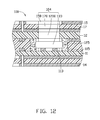
- FIG. 12 similar to FIG. 11 , but showing a cavity is defined.
- the method includes the steps in no particular order of:
- first substrate comprising a first electrically conductive layer, the first electrically conductive layer comprising an exposed portion and a laminating portion surrounding the exposed portion;
- a first substrate 11 is provided.
- the first substrate 11 includes a first electrically conductive layer 110 , a first insulating layer 111 , and a second electrically conductive layer 112 .
- the first insulating layer 111 is sandwiched between the first and second electrically conductive layers 110 and 112 .
- the first electrically conductive layer 110 defines an exposed portion 113 and a laminating portion 114 surrounding the exposed portion 113 .
- the first electrically conductive layer 110 defines circuit pattern therein, at least one solder pad is defined in the exposed portion 113 of the first electrically conductive layer 110 .
- the exposed portion 113 is rectangular, and the second electrically conductive layer 112 with a circuit pattern defined therein.
- the first rigid substrate 11 is a double-sided copper clad laminate (CCL), and both of the first and second electrically conductive layers 110 , 112 are patterned copper foils.
- CCL copper clad laminate
- circuit pattern of the laminating portion 114 is not shown in FIG. 1 .
- step (2) a second substrate 12 is provided.
- the second substrate 12 includes an unwanted portion 120 and a preserving portion 121 surrounding the unwanted portion 120 .
- the unwanted portion 120 corresponds to the exposed portion 113 and is rectangular.
- the preserving portion 121 corresponds to the laminating portion 114 .
- the second substrate 12 includes a third electrically conductive layer 122 , a second insulating layer 123 , and a fourth electrically conductive layer 124 .
- the second insulating layer 123 is sandwiched between the third and fourth electrically conductive layers 122 and 124 .
- the third electrically conductive layer 122 defines circuit pattern therein.
- the fourth electrically conductive layer 124 can define a circuit pattern therein.
- the second substrate 12 is a double-sided copper clad laminate (CCL), and both of the third and fourth electrically conductive layers 122 and 124 are patterned copper foils.
- CCL copper clad laminate
- the first substrates 11 can also be a single sided copper clad laminate or a multi-layered printed circuit board.
- the second substrates 12 can also be a single sided copper clad laminate or a multi-layered printed circuit board.
- a first annular bump 115 extending along an imaginary boundary line of the exposed portion 113 of the first substrate 11 is formed at the first substrate 11 .
- the first annular bump 115 is formed on the first insulating layer 111 .
- the first annular bump 115 is rectangular.
- the first annular bump 115 can be formed by the following steps. First, a screen printer and a printing ink are provided.
- the screen printer includes a base, a screen, and a scraper.
- the base is adapted for setting the first substrate 11 .
- the screen is used for setting the printing ink and defines an annular leaking slot corresponding to the first annular bump 115 .
- the scraper is configured for scraping the printing ink on the screen to make the printing ink leak from the screen to the first substrate 11 via the annular leaking slot.
- the printing ink is a material such as polyimide (PI), TEFLON, polyamide (PA), polymethylmethacrylate (PMMA), polycarbonate (PC), polyethylene terephthalate (PET), and polyamide polyethylene-terephthalate copolymer or any combination thereof.
- the printing ink is set on the screen.
- the first substrate 11 is deposited on the base with the first electrically conductive layer 110 facing to the screen.
- the printing ink is scraped by the scraper and leaks from the screen to the first substrate 11 via the annular leaking slot, thus the first annular bump 115 is obtained.
- the first annular bump 115 is baked and fully cured.
- a second annular bump 125 is formed on the second substrate 12 .
- the second annular bump 125 is formed on the second insulating layer 123 , surrounds an boundary line of the unwanted portion 120 , and corresponds to the first annular bump 115 .
- the first and second annular bumps 115 , 125 are all formed by screen printing.
- the formation of the second annular bump 125 is similar to the formation of the first annular bump 115 .
- a first adhesive layer 13 is provided.
- the first adhesive layer 13 includes a first adhesive surface 130 and an opposite second adhesive surface 131 .
- the first adhesive layer 13 defines an opening 132 through the first and second adhesive surfaces 130 and 131 .
- the opening 132 generally corresponds to the exposed portion 113 .
- a cross-section area of the opening 132 is bigger than that of the exposed portion 113 .
- a material of the first adhesive layer 13 is the same as that of the first and second annular bumps 115 and 125 .
- step (6) the first and second substrates 11 , 12 , and the first adhesive layer 13 are laminated together to form a laminated structure 102 , wherein the first adhesive layer 13 is sandwiched between the first and second substrates 11 and 12 .
- the exposed portion 113 and the unwanted portion 120 are all exposed in the opening 132 , and the second annular bump 125 is in contact with the first annular bump 115 .
- the first substrate 11 , the first adhesive layer 13 , and the second substrate 12 are aligned with each other and stacked one on another in that order to form a stacked structure 101 shown in FIG. 8 .
- the first adhesive surface 130 of the first adhesive layer 13 is in contact with the first electrically conductive layer 110
- the second adhesive surface 131 is in contact with the third electrically conductive layer 122 .
- the exposed portion 113 is opposite to the unwanted portion 120 .
- the laminating portion 114 is opposite to the preserving portion 121 .
- the second annular bump 125 is opposite to the first annular bump 115 , and at least a portion of each of the first and second annular bumps 115 and 125 can be received in the opening 132 of the first adhesive layer 13 .
- the summation of the heights of the first and second annular bumps 115 , 125 is less than the distance between the first insulating layer 111 and the second insulating layer 123 .
- the stacked structure 101 is compressed, thus a laminated structure 102 shown in FIG. 9 is obtained.
- the second annular bump 125 is in contact with and bonds with the first annular bump 115 , the first annular bump 115 , the second annular bump 125 , the first insulating layer 111 , and the second insulating layer 123 define a cavern 133 .
- the material of the first adhesive layer 13 is intenerated and flows, to fill the gap between the first and second insulating layers 111 , 123 except for the cavern 133 .
- the first adhesive layer 13 binds the preserving portion 121 and the laminating portion 114 together.
- the distance between the first insulating layer 111 and the second insulating layer 123 decreases, thus in the laminated structure 102 , the second annular bump 125 is in contact with the first annular bump 115 . That is, the summation of the heights of the first and second annular bumps 115 , 125 is equal to the distance between the first insulating layer 111 and the second insulating layer 123 .
- annular bump formed on the first substrate 11 or the second substrate 12 Only one annular bump formed on the first substrate 11 or the second substrate 12 will also work. For example, only an annular bump surrounding the exposed portion 113 of the first substrate 11 is formed on the first insulated layer 111 , and no annular bump is formed on the second substrate 12 . At least a portion of the annular bump is received in the opening 132 in the stacked structure 101 and the annular bump is in contact with the second insulated layer 123 in the laminated structure 102 . The height of the annular bump is less than the distance between the first insulating layer 111 and the second insulating layer 123 in the stacked structure 101 , the height of the bump is equal to the distance between the first insulating layer 111 and the second insulating layer 123 in the laminated structure 102 . The situation is the same when only one annular bump extending along the unwanted portion 120 of the second substrate 12 is formed on the second insulated layer 123 .
- a third substrate 14 , a fourth substrate 15 , a second adhesive layer 16 , and a third adhesive layer 17 are laminated to the laminated structure 102 prior to step (5).
- Both of the third and fourth substrates 14 and 15 include at least one electrically conductive layer.
- the third and fourth substrates 14 and 15 are copper foils.
- the second and third adhesive layers 16 and 17 can be a material the same as that of the first adhesive layer 13 .
- the third substrate 14 and the second adhesive layer 16 are laminated onto the first substrate 11 of the laminated structure 102 , the second adhesive layer 16 is sandwiched between the third substrate 14 and the first substrate 11 .
- the fourth substrate 15 and the third adhesive layer 17 are laminated onto the second substrate 12 , wherein the third adhesive layer 17 is sandwiched between the fourth substrate 15 and the second substrate 12 .
- a multilayer substrate 103 is obtained.
- the lamination of the third and fourth substrates 14 , 15 to the laminated structure 102 includes a step of stacking the third substrate 14 , the second adhesive layer 16 , the laminated structure 102 , the fourth substrate 15 , and the third adhesive layer 17 one on the other in that order, and a step of compressing the combined the third substrate 14 , the second adhesive layer 16 , the laminated structure 102 , the fourth substrate 15 , and the third adhesive layer 17 .
- the third and fourth substrates 14 and 15 can also be a single-sided CCL or a double-sided CCL.
- the third and fourth substrates 14 and 15 are patterned to form circuits thereon, thus a first electrically conductive pattern 140 and a second electrically conductive pattern 150 are obtained. Furthermore, a plurality of plated through holes can be formed in the multilayer substrate 103 to electrically connect the first electrically conductive pattern 140 , the second electrically conductive layer 112 , the second electrically conductive pattern 150 , and the fourth electrically conductive layer 124 .
- a cavity 104 is defined in the laminated structure 103 , by removing a portion of the fourth substrate 15 , a portion of the third adhesive layer 17 , and the unwanted portion 120 above the cavern 133 .
- a laser beam, a milling cutter, or other means can be used to cut the fourth substrate 15 , third adhesive layer 17 , and the second substrate 12 along the imaginary boundary lines between the unwanted portion 120 and the preserving portion 121 .
- the imaginary boundary lines between the unwanted portion 120 and the preserving portion 121 corresponds to the borderlines between the exposed portion 113 and the laminating portion 114 of the first substrate 11 .
- a first slit 150 is defined after a portion of the fourth substrate 15 above the cavern 133 is removed.
- a second slit 170 is defined after a portion of the third adhesive layer 17 above the cavern 133 is removed.
- a third slit 1200 in communication with the cavern 133 is defined after the unwanted portion 120 above the cavern 133 is removed.
- the first slit 150 , the second slit 170 , the third slit 1200 , and the cavern 133 compose the cavity 104 , thus a printed circuit board 100 with the cavity 104 is obtained.
- the exposed portion 113 is exposed in the cavity 104 , thus an electronic component, such as a chip, can be installed in the cavity 104 and in electrically communication with the solder pad in the first electrically conductive layer 110 .
- the first annular bump 115 and the second annular bumps 125 are formed on the first and second substrates 11 , 12 prior to the laminating step.
- the first and second annular bumps 115 , 125 can prevent the material of the first adhesive layer 13 from flowing into the cavern 133 to contaminate the exposed portion 113 during the laminating process.
- no protecting glue is needed to protect the exposed portion 113 before being laminated, no extra removing process is needed after the unwanted portion 120 of the second substrate 12 is removed.
- the cost is decreased, the manufacturing of the printed circuit board with cavity is simplified, and the reliability of the connection between the solder pad and the electronic component is increased.
Landscapes
- Engineering & Computer Science (AREA)
- Manufacturing & Machinery (AREA)
- Microelectronics & Electronic Packaging (AREA)
- Production Of Multi-Layered Print Wiring Board (AREA)
- Structure Of Printed Boards (AREA)
Abstract
Description
Claims (8)
Applications Claiming Priority (3)
| Application Number | Priority Date | Filing Date | Title |
|---|---|---|---|
| CN201010195875.3 | 2010-06-10 | ||
| CN2010101958753A CN102281725B (en) | 2010-06-10 | 2010-06-10 | Manufacturing method for circuit board |
| CN201010195875 | 2010-06-10 |
Publications (2)
| Publication Number | Publication Date |
|---|---|
| US20110302775A1 US20110302775A1 (en) | 2011-12-15 |
| US8978244B2 true US8978244B2 (en) | 2015-03-17 |
Family
ID=45095015
Family Applications (1)
| Application Number | Title | Priority Date | Filing Date |
|---|---|---|---|
| US13/116,001 Active 2034-01-15 US8978244B2 (en) | 2010-06-10 | 2011-05-26 | Method for manufacturing printed circuit board |
Country Status (2)
| Country | Link |
|---|---|
| US (1) | US8978244B2 (en) |
| CN (1) | CN102281725B (en) |
Cited By (1)
| Publication number | Priority date | Publication date | Assignee | Title |
|---|---|---|---|---|
| US20150156862A1 (en) * | 2013-06-20 | 2015-06-04 | Commissariat A L'energie Atomique Et Aux Ene Alt | Method for producing a mechanically autonomous microelectronic device |
Families Citing this family (13)
| Publication number | Priority date | Publication date | Assignee | Title |
|---|---|---|---|---|
| CN103929884A (en) * | 2013-01-16 | 2014-07-16 | 深圳市牧泰莱电路技术有限公司 | Method for manufacturing printed circuit board with step slotted hole |
| CN104254190B (en) * | 2013-06-26 | 2017-12-01 | 陈丽专 | The preparation method of circuit board |
| CN104902676A (en) * | 2014-03-06 | 2015-09-09 | 常熟东南相互电子有限公司 | Printed circuit board and manufacturing method thereof |
| CN105101609B (en) * | 2014-05-08 | 2018-01-30 | 先丰通讯股份有限公司 | Interior space sets up the circuit board of formula |
| CN105611751B (en) * | 2015-09-07 | 2019-02-19 | 瑞华高科技电子工业园(厦门)有限公司 | A kind of processing method of multi-layer flexible circuit board |
| CN105828516A (en) * | 2016-05-06 | 2016-08-03 | 鹤山市中富兴业电路有限公司 | Flexible plate for protecting bare copper layer, and production method thereof |
| CN106231796A (en) * | 2016-07-29 | 2016-12-14 | 台山市精诚达电路有限公司 | The multilamellar soft board ends-opening method that internal layer is windowed |
| CN107241857B (en) * | 2017-06-27 | 2019-08-13 | 华为技术有限公司 | A kind of printed circuit board and communication equipment |
| US10888002B2 (en) * | 2019-03-28 | 2021-01-05 | At&S Austria Technologie & Systemtechnik Aktiengesellschaft | Component carrier with embedded tracks protruding up to different heights |
| CN210579428U (en) * | 2019-06-20 | 2020-05-19 | 深圳Tcl数字技术有限公司 | Circuit board and display device |
| US10667394B1 (en) | 2019-09-24 | 2020-05-26 | Gentherm Inc. | Double-sided, single conductor laminated substrate |
| CN110572958B (en) * | 2019-09-26 | 2023-06-30 | 九江明阳电路科技有限公司 | Rigid-flex printed circuit board lamination structure and manufacturing method |
| CN112218428B (en) * | 2020-11-04 | 2022-02-18 | 生益电子股份有限公司 | Manufacturing method of embedded cavity and PCB |
Citations (6)
| Publication number | Priority date | Publication date | Assignee | Title |
|---|---|---|---|---|
| US5622588A (en) * | 1995-02-02 | 1997-04-22 | Hestia Technologies, Inc. | Methods of making multi-tier laminate substrates for electronic device packaging |
| JPH09148749A (en) | 1995-11-20 | 1997-06-06 | Sumise Device:Kk | Cavity forming method of multilayer circuit board |
| US6329609B1 (en) * | 2000-06-29 | 2001-12-11 | International Business Machines Corporation | Method and structure to prevent distortion and expansion of organic spacer layer for thin film transfer-join technology |
| JP2005268416A (en) | 2004-03-17 | 2005-09-29 | Fujikura Ltd | Printed wiring board and producing method thereof |
| US7562446B2 (en) * | 2005-09-22 | 2009-07-21 | Samsung Electro-Mechanics Co., Ltd. | Method for manufacturing substrate with cavity |
| CN201369335Y (en) | 2008-10-15 | 2009-12-23 | 太聚能源股份有限公司 | Photovoltaic cell module |
Family Cites Families (4)
| Publication number | Priority date | Publication date | Assignee | Title |
|---|---|---|---|---|
| TW200740334A (en) * | 2005-10-20 | 2007-10-16 | Matsushita Electric Ind Co Ltd | Multilayer printed wiring board and its manufacturing method |
| CN101431863B (en) * | 2007-11-05 | 2010-12-08 | 富葵精密组件(深圳)有限公司 | Back glue attaching method for flexible printed circuit board |
| KR100887685B1 (en) * | 2007-11-15 | 2009-03-11 | 삼성전기주식회사 | Method for manufacturing printed circuit board having embedded electronic components |
| KR101003640B1 (en) * | 2008-06-16 | 2010-12-23 | 삼성전기주식회사 | Chip embedded printed circuit board and manufacturing method thereof |
-
2010
- 2010-06-10 CN CN2010101958753A patent/CN102281725B/en active Active
-
2011
- 2011-05-26 US US13/116,001 patent/US8978244B2/en active Active
Patent Citations (6)
| Publication number | Priority date | Publication date | Assignee | Title |
|---|---|---|---|---|
| US5622588A (en) * | 1995-02-02 | 1997-04-22 | Hestia Technologies, Inc. | Methods of making multi-tier laminate substrates for electronic device packaging |
| JPH09148749A (en) | 1995-11-20 | 1997-06-06 | Sumise Device:Kk | Cavity forming method of multilayer circuit board |
| US6329609B1 (en) * | 2000-06-29 | 2001-12-11 | International Business Machines Corporation | Method and structure to prevent distortion and expansion of organic spacer layer for thin film transfer-join technology |
| JP2005268416A (en) | 2004-03-17 | 2005-09-29 | Fujikura Ltd | Printed wiring board and producing method thereof |
| US7562446B2 (en) * | 2005-09-22 | 2009-07-21 | Samsung Electro-Mechanics Co., Ltd. | Method for manufacturing substrate with cavity |
| CN201369335Y (en) | 2008-10-15 | 2009-12-23 | 太聚能源股份有限公司 | Photovoltaic cell module |
Cited By (2)
| Publication number | Priority date | Publication date | Assignee | Title |
|---|---|---|---|---|
| US20150156862A1 (en) * | 2013-06-20 | 2015-06-04 | Commissariat A L'energie Atomique Et Aux Ene Alt | Method for producing a mechanically autonomous microelectronic device |
| US9674939B2 (en) * | 2013-06-20 | 2017-06-06 | Commissariat A L'energie Atomique Et Aux Energies Alternatives | Method for producing a mechanically autonomous microelectronic device |
Also Published As
| Publication number | Publication date |
|---|---|
| CN102281725B (en) | 2013-03-20 |
| CN102281725A (en) | 2011-12-14 |
| US20110302775A1 (en) | 2011-12-15 |
Similar Documents
| Publication | Publication Date | Title |
|---|---|---|
| US8978244B2 (en) | Method for manufacturing printed circuit board | |
| US9999134B2 (en) | Self-decap cavity fabrication process and structure | |
| US8383948B2 (en) | Flex-rigid wiring board and method for manufacturing the same | |
| US9345142B2 (en) | Chip embedded board and method of manufacturing the same | |
| US9743533B2 (en) | Method for manufacturing rigid-flexible printed circuit board | |
| TWI448223B (en) | Multilayer printed circuit board and method for manufacturing same | |
| CN103458628A (en) | Multi-layer circuit board and manufacturing method thereof | |
| US10064292B2 (en) | Recessed cavity in printed circuit board protected by LPI | |
| US10477704B2 (en) | Multilayer board and electronic device | |
| KR20160099934A (en) | Rigid-flexible printed circuit board and method for manufacturing the same | |
| US10772220B2 (en) | Dummy core restrict resin process and structure | |
| CN101422091B (en) | Multilayer circuit board having cable section, and manufacturing method thereof | |
| JP2004186235A (en) | Wiring board and method for manufacturing the same | |
| CN113747654B (en) | Flexible circuit board and manufacturing method thereof | |
| CN103889169A (en) | Circuit board and manufacturing method thereof | |
| KR20120097327A (en) | Multilayer wiring substrate | |
| US20220336230A1 (en) | Interposer, manufacturing method therefor, and circuit board assembly | |
| JP2005123332A (en) | Circuit board and method of manufacturing thereof | |
| CN107889356B (en) | Soft and hard composite circuit board | |
| KR20140148111A (en) | Rigid flexible printed circuit board and method for manufacturing thereof | |
| US11910540B2 (en) | Circuit board with solder mask on internal copper pad | |
| TWI778356B (en) | Rigid-flexible circuit board and method of manufacturing the same | |
| KR101519153B1 (en) | A printed circuit board and method for manufacturing the same | |
| JP2007059702A (en) | Circuit wiring board and its manufacturing method | |
| KR101936415B1 (en) | Manufacturing method for copper clad laminates using conductive polymer ball |
Legal Events
| Date | Code | Title | Description |
|---|---|---|---|
| AS | Assignment |
Owner name: FUKUI PRECISION COMPONENT (SHENZHEN) CO., LTD., CH Free format text: ASSIGNMENT OF ASSIGNORS INTEREST;ASSIGNORS:CAI, XUE-JUN;LI, ZHI-YONG;LIU, CHAO;REEL/FRAME:026340/0065 Effective date: 20110517 Owner name: FOXCONN ADVANCED TECHNOLOGY INC., TAIWAN Free format text: ASSIGNMENT OF ASSIGNORS INTEREST;ASSIGNORS:CAI, XUE-JUN;LI, ZHI-YONG;LIU, CHAO;REEL/FRAME:026340/0065 Effective date: 20110517 |
|
| AS | Assignment |
Owner name: ZHEN DING TECHNOLOGY CO., LTD., TAIWAN Free format text: CHANGE OF NAME;ASSIGNOR:FOXCONN ADVANCED TECHNOLOGY INC.;REEL/FRAME:026895/0558 Effective date: 20110613 |
|
| STCF | Information on status: patent grant |
Free format text: PATENTED CASE |
|
| CC | Certificate of correction | ||
| AS | Assignment |
Owner name: GARUDA TECHNOLOGY CO., LTD, TAIWAN Free format text: ASSIGNMENT OF ASSIGNORS INTEREST;ASSIGNORS:FUKUI PRECISION COMPONENT (SHENZHEN) CO., LTD.;ZHEN DING TECHNOLOGY CO., LTD.;REEL/FRAME:040978/0744 Effective date: 20170101 Owner name: FUKUI PRECISION COMPONENT (SHENZHEN) CO., LTD., CH Free format text: ASSIGNMENT OF ASSIGNORS INTEREST;ASSIGNORS:FUKUI PRECISION COMPONENT (SHENZHEN) CO., LTD.;ZHEN DING TECHNOLOGY CO., LTD.;REEL/FRAME:040978/0744 Effective date: 20170101 |
|
| AS | Assignment |
Owner name: AVARY HOLDING (SHENZHEN) CO., LIMITED., CHINA Free format text: CHANGE OF NAME;ASSIGNOR:FUKUI PRECISION COMPONENT (SHENZHEN) CO., LTD.;REEL/FRAME:043340/0450 Effective date: 20170524 |
|
| AS | Assignment |
Owner name: AVARY HOLDING (SHENZHEN) CO., LIMITED., CHINA Free format text: CHANGE OF NAME;ASSIGNOR:FUKUI PRECISION COMPONENT (SHENZHEN) CO., LTD.;REEL/FRAME:043378/0038 Effective date: 20170524 |
|
| MAFP | Maintenance fee payment |
Free format text: PAYMENT OF MAINTENANCE FEE, 4TH YEAR, LARGE ENTITY (ORIGINAL EVENT CODE: M1551) Year of fee payment: 4 |
|
| MAFP | Maintenance fee payment |
Free format text: PAYMENT OF MAINTENANCE FEE, 8TH YEAR, LARGE ENTITY (ORIGINAL EVENT CODE: M1552); ENTITY STATUS OF PATENT OWNER: LARGE ENTITY Year of fee payment: 8 |