US8896547B2 - Pointer detection apparatus and pointer detection method - Google Patents
Pointer detection apparatus and pointer detection method Download PDFInfo
- Publication number
- US8896547B2 US8896547B2 US12/750,502 US75050210A US8896547B2 US 8896547 B2 US8896547 B2 US 8896547B2 US 75050210 A US75050210 A US 75050210A US 8896547 B2 US8896547 B2 US 8896547B2
- Authority
- US
- United States
- Prior art keywords
- conductors
- reception
- signals
- transmission
- conductor
- Prior art date
- Legal status (The legal status is an assumption and is not a legal conclusion. Google has not performed a legal analysis and makes no representation as to the accuracy of the status listed.)
- Active, expires
Links
Images


Classifications
-
- G—PHYSICS
- G06—COMPUTING OR CALCULATING; COUNTING
- G06F—ELECTRIC DIGITAL DATA PROCESSING
- G06F3/00—Input arrangements for transferring data to be processed into a form capable of being handled by the computer; Output arrangements for transferring data from processing unit to output unit, e.g. interface arrangements
- G06F3/01—Input arrangements or combined input and output arrangements for interaction between user and computer
- G06F3/03—Arrangements for converting the position or the displacement of a member into a coded form
- G06F3/041—Digitisers, e.g. for touch screens or touch pads, characterised by the transducing means
- G06F3/044—Digitisers, e.g. for touch screens or touch pads, characterised by the transducing means by capacitive means
- G06F3/0445—Digitisers, e.g. for touch screens or touch pads, characterised by the transducing means by capacitive means using two or more layers of sensing electrodes, e.g. using two layers of electrodes separated by a dielectric layer
-
- G—PHYSICS
- G06—COMPUTING OR CALCULATING; COUNTING
- G06F—ELECTRIC DIGITAL DATA PROCESSING
- G06F3/00—Input arrangements for transferring data to be processed into a form capable of being handled by the computer; Output arrangements for transferring data from processing unit to output unit, e.g. interface arrangements
- G06F3/01—Input arrangements or combined input and output arrangements for interaction between user and computer
- G06F3/03—Arrangements for converting the position or the displacement of a member into a coded form
- G06F3/041—Digitisers, e.g. for touch screens or touch pads, characterised by the transducing means
- G06F3/044—Digitisers, e.g. for touch screens or touch pads, characterised by the transducing means by capacitive means
- G06F3/0446—Digitisers, e.g. for touch screens or touch pads, characterised by the transducing means by capacitive means using a grid-like structure of electrodes in at least two directions, e.g. using row and column electrodes
-
- G—PHYSICS
- G06—COMPUTING OR CALCULATING; COUNTING
- G06F—ELECTRIC DIGITAL DATA PROCESSING
- G06F3/00—Input arrangements for transferring data to be processed into a form capable of being handled by the computer; Output arrangements for transferring data from processing unit to output unit, e.g. interface arrangements
- G06F3/01—Input arrangements or combined input and output arrangements for interaction between user and computer
- G06F3/03—Arrangements for converting the position or the displacement of a member into a coded form
- G06F3/041—Digitisers, e.g. for touch screens or touch pads, characterised by the transducing means
- G06F3/044—Digitisers, e.g. for touch screens or touch pads, characterised by the transducing means by capacitive means
- G06F3/0448—Details of the electrode shape, e.g. for enhancing the detection of touches, for generating specific electric field shapes, for enhancing display quality
-
- G—PHYSICS
- G06—COMPUTING OR CALCULATING; COUNTING
- G06F—ELECTRIC DIGITAL DATA PROCESSING
- G06F3/00—Input arrangements for transferring data to be processed into a form capable of being handled by the computer; Output arrangements for transferring data from processing unit to output unit, e.g. interface arrangements
- G06F3/01—Input arrangements or combined input and output arrangements for interaction between user and computer
- G06F3/03—Arrangements for converting the position or the displacement of a member into a coded form
- G06F3/041—Digitisers, e.g. for touch screens or touch pads, characterised by the transducing means
- G06F3/046—Digitisers, e.g. for touch screens or touch pads, characterised by the transducing means by electromagnetic means
-
- G—PHYSICS
- G06—COMPUTING OR CALCULATING; COUNTING
- G06F—ELECTRIC DIGITAL DATA PROCESSING
- G06F2203/00—Indexing scheme relating to G06F3/00 - G06F3/048
- G06F2203/041—Indexing scheme relating to G06F3/041 - G06F3/045
- G06F2203/04111—Cross over in capacitive digitiser, i.e. details of structures for connecting electrodes of the sensing pattern where the connections cross each other, e.g. bridge structures comprising an insulating layer, or vias through substrate
Definitions
- the present invention makes it possible for a pointer detection apparatus of the electrostatic coupling system to carry out position detection of multiple positions (i.e., multiple positions of multiple pointers, or of multiple fingers of one or more users) at the same time.
- FIG. 13 is a flow chart illustrating a procedure for position detection by the pointer detection apparatus of FIG. 1 ;
- FIG. 23 is a schematic circuit diagram illustrating a supplying form of periodic signals according to modification 8 to the pointer detection apparatus of FIG. 1 ;
- FIGS. 26A to 26C are diagrammatic views illustrating another example of rotation of the frequencies of periodic signals according to modification 9 to the pointer detection apparatus of FIG. 1 ;
- FIG. 28 is a similar view but illustrating an example of a supplying form of periodic signals and a detection form of an output signal according to modification 10 to the pointer detection apparatus of FIG. 1 ;
- FIG. 44A is a diagrammatic view illustrating a supplying form of periodic signals upon double-sided transmission according to modification 19 to the pointer detection apparatus of FIG. 1 and FIG. 44B is a diagrammatic view illustrating the level of output signals;
- FIG. 47 is a schematic block diagram of a pointer detection apparatus according to a second embodiment of the present invention.
- FIGS. 49A and 49B are diagrammatic views illustrating switching operation of transmission conductors of the pointer detection apparatus of FIG. 47 ;
- FIG. 51 is a diagrammatic view illustrating switching operation of reception conductors by the pointer detection apparatus of FIG. 47 ;
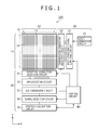
- a first embodiment of the present invention relates to a basic configuration of a pointer detection apparatus and a pointer detection method of the present invention.
- FIG. 1 shows a general configuration of the pointer detection apparatus according to the first embodiment of the present invention.
- the number of transmission conductors 14 is 64 and the number of reception conductors 12 is 128. Further, the disposition distance, that is, the pitch, of both of the transmission conductors 14 and the reception conductors 12 is 3.2 mm.
- the present invention is not limited to the configuration just described, and the number and the pitch of each of the transmission conductors 14 and the reception conductors 12 is set suitably in accordance with the size of the sensor section 10 , required detection accuracy, and so forth.
- FIG. 3 shows an example of a general configuration of the multi-frequency signal supplying circuit 21 .
- the multi-frequency signal supplying circuit 21 in the first embodiment includes a number of periodic signal production sections 24 equal to the number of the transmission blocks of the reception conductor group 11 , that is, 16 periodic signal production sections 24 .
- the periodic signal production sections 24 individually produce a periodic signal of a fixed period under the control of the control circuit 40 .
- the periodic signals produced by the periodic signal production sections 24 are denoted by indexes i from “0” to “15” in order beginning with that of the periodic signal production sections 24 that is positioned nearest to the reception section 30 .
- the 16 periodic signals have 16 different frequencies different by 10 kHz from each other, for example, from 100 kHz to 250 kHz.
- the selected one of the transmission conductors 14 is changed over by the transmission conductor selection circuit 22 under the control of the control circuit 40 .
- the transmission conductor selection circuit 22 in the first embodiment is formed of a number of switches equal to the number of groups of the transmission conductor group 13 , that is, of 16 switches.
- FIG. 5 shows an internal configuration of the transmission conductor selection circuit 22 .
- the transmission conductor selection circuit 22 includes a plurality of switches 22 a for selectively supplying a periodic signal supplied thereto from the multi-frequency signal supplying circuit 21 .
- the switches 22 a are provided in a one-by-one corresponding relationship to transmission blocks 25 .
- Each of the switches 22 a has four terminals 22 b on the output side thereof, which are individually connected to corresponding ones of the transmission conductors 14 .
- Each of the switches 22 a has one terminal 22 c on the input side thereof, which is connected to an output terminal of a corresponding one of the periodic signal production sections 24 of the multi-frequency signal supplying circuit 21 shown in FIG. 3 .
- frequency signals output from the periodic signal production sections 24 of the multi-frequency signal supplying circuit 21 and having different frequencies are supplied at the same time to the 16 transmission conductors 14 after the changeover to carry out position detection. This series of operations is repeated to carry out position detection of at least one pointer.
- FIG. 7 shows a general configuration of the reception conductor selection circuit 31 and associated elements.
- the reception conductor selection circuit 31 includes a plurality of switches 31 a .
- the switches 31 a are provided in a one-by-one corresponding relationship with the detection blocks 36 .
- Each of the switches 31 a has eight terminals 31 b on the input side thereof, which are connected to corresponding ones of the reception conductors 12 .
- Each of the switches 31 a has a terminal 31 c on the output side thereof, which is connected to an input terminal of a corresponding one of I/V conversion circuits 32 a hereinafter described.
- the reception conductor 12 is capacitively coupled not only to the transmission conductor 14 but also to the ground through the finger 19 .
- part of an electric field emerging from the transmission conductor 14 converges to the finger 19 and part of current flowing between the transmission conductor 14 and the reception conductor 12 flows to the ground through the finger 19 .
- the value of current flowing into the reception conductor 12 decreases.
- a variation of the value of current output from the reception conductor 12 is detected by the reception section 30 to detect the position of the pointer.
- each of the periodic signal production sections 24 in the multi-frequency signal supplying circuit 21 sets a periodic signal of a frequency allocated thereto by the control circuit 40 at step S 1 .
- step S 9 the control circuit 40 decides at step S 9 whether or not the position detection with regard to all reception conductors 12 is completed. If the position detection with regard to all reception conductors 12 is not completed, (the result of the decision at step S 9 is NO), the processing returns to step S 2 , at which the switches 31 a of the detection blocks 36 in the reception conductor selection circuit 31 are changed over to select the reception conductors 12 different from those in the preceding operation cycle.
- the transmission conductor group 13 and the reception conductor group 11 are each divided into 16 groups and the groups are processed in parallel to each other. Therefore, in the present embodiment, the detection time can be reduced, for example, to 1/(16 ⁇ 16) in comparison with the detection time where a detection process is carried out successively for all cross points as in the prior art.
- the number of groups is not limited to the specific number mentioned above, and an effect of reduction of the detection time can be obtained even if only one of the transmission conductor group 13 and the reception conductor group 11 is divided into groups.
- the sensor section 50 includes a glass substrate 51 , a plurality of transmission conductors 52 formed on one of surfaces of the glass substrate 51 , on the lower face of the glass substrate 51 in FIG. 14 , and a first protective layer 53 formed on the transmission conductors 52 .
- the sensor section 50 further includes a plurality of reception conductors 54 formed on the other surface of the glass substrate 51 , on the upper surface of the glass substrate 51 in FIG. 14 , a second protective layer 55 formed on the reception conductors 54 , and a protective sheet 56 formed on the second protective layer 55 .
- the detection surface for a pointer in the present example is a surface of the sensor section 50 on the protective sheet 56 side.
- the metal sections 62 are substantially linear metal members formed, for example, by drawing a metal material in a direction perpendicular to the direction in which the reception conductors 65 extend.
- the insulating sections 63 are formed so as to cover over part of the metal sections 62 .
- the transmission conductors 64 are provided at the opposite ends in the drawing direction of the metal sections 62 and are electrically connected to each other by the metal sections 62 .
- the reception conductors 65 are formed so as to stretch over the insulating sections 63 , such that the reception conductors 65 are electrically isolated from the metal sections 62 and transmission conductors 64 .
- the reception conductors 65 are formed from a linear conductor similar to the first embodiment described above. Meanwhile, the transmission conductors 64 are formed so as to be connected to the metal sections 62 through openings in the insulating sections 63 . In particular, the transmission conductors 64 , to which periodic signals are supplied, are disposed three-dimensionally such that they pass below the reception conductors 65 with the insulating sections 63 sandwiched therebetween.
- the glass substrate 61 , transmission conductors 64 and reception conductors 65 are formed from materials similar to those which are used in the first embodiment described above.
- the glass substrate 61 may be replaced with a sheet-like or film-like substrate formed from a synthetic resin material similarly as in the first embodiment.
- the transmission conductors and the reception conductors can be individually formed from a linear conductor of a fixed width extending in a predetermined direction.
- the shape of the transmission conductors and the reception conductors in the present invention is not limited to a linear shape extending in a predetermined direction.
- Another example of a configuration of the transmission conductors is described below as modification 3.
- the reception conductors 74 are formed from a linear conductor of a fixed width as seen in FIG. 16A .
- the transmission conductors 71 A are formed from a linear conductor portion 72 and land conductor portions 73 A having a width greater than that of the linear conductor portion 72 and made of ITO or the like.
- a transmission conductor 71 B includes a linear conductor portion 72 and a land conductor portion 73 B modified from that in modification 3.
- the sensor section 70 B is different from that of modification 3 in that, while the land conductor portion 73 A in modification 3 has the first and second land portions 73 b and 73 c of a substantially triangular shape, the land conductor portion 73 A in the present example has first and second land portions 73 g and 73 h having a substantially trapezoidal shape.
- the sensor section 80 in modification 5 is suitable for detection, for example, of rotational operation.
- FIGS. 21A and 21B An example is shown in FIGS. 21A and 21B .
- elements like those in the first embodiment described above with reference to FIG. 7 are denoted by like reference characters and overlapping description of them is omitted herein to avoid redundancy.
- FIG. 21A shows a general configuration of an amplifier according to modification 6, and FIG. 21B shows a general configuration of an amplification circuit and peripheral circuits where a differential amplifier is used.
- the reception conductor group 11 is divided into detection blocks ⁇ X 0 to X 8 ⁇ , ⁇ X 8 to X 15 ⁇ , . . . , ⁇ X 114 to X 121 ⁇ and ⁇ X 121 to X 128 ⁇ .
- the one of the I/V conversion circuits 32 a which is connected to the output terminal of the switch 88 a , is connected to the negated input terminal, which has the negative polarity ( ⁇ ), of a differential amplifier 85 .
- the other I/V conversion circuit 32 a connected to the output terminal of the switch 88 b , is connected to the non-negated input terminal, which has the positive polarity (+), of the differential amplifier 85 .
- the paired switches 88 a and 88 b are structured such that those reception conductors 12 , which are to be connected to the IN conversion circuits 32 a , are changed over at predetermined time intervals.
- the switches 88 a and 88 b are changed over after a predetermined time interval such that the switch 88 a is connected to the reception conductor X 1 and the switch 88 b is connected to the reception conductor X 2 . Thereafter, the conductors to be connected are successively changed over at predetermined time intervals.
- the differential amplifier 85 is used in the reception section, since noise included in outputs from the reception conductors 12 is canceled by the differential amplifiers 85 , the noise resisting property can be improved.
- the reception conductor which is positioned at the center of a plurality of reception conductors connected to the differential amplifier 86 is set to a reference voltage level or the zero voltage as in modification 7, even if the pointer is not grounded sufficiently, as long as the pointer is positioned in proximity to the reception conductor X m , part of the current can be shunted through both the pointer and the reception conductor X m . As a result, the decrease in the sensitivity described above can be minimized.
- FIG. 23 illustrates a supplying form of a periodic signal in modification 8.
- modification 8 is configured such that, between the multi-frequency signal supplying circuit 21 and the transmission conductor selection circuit 22 of the transmission section 20 shown in FIG. 1 , a phase inversion circuit 87 for inversing the phase of a periodic signal produced by each periodic signal production section 24 is provided.
- the phase inversion circuit 87 inverses the phase of the periodic signal of the frequency f k and supplies the periodic signal of the inversed phase to a transmission conductor Y n .
- FIG. 24 illustrates a supplying form of a periodic signal and a detection form of an output signal according to modification 9.
- a two-input one-output amplifier 90 with two inputs being non-negated (+) terminals is used in the reception section 30 . Where the amplifier 90 is used, periodic signals of the same frequency are supplied to two transmission conductors 14 .
- periodic signals of the same frequency are supplied in a unit of two transmission conductors 14 , while output signals of two reception conductors 12 are added in the reception section.
- the number of transmission conductors 14 to which periodic signals of the same frequency are to be supplied, may be three or more, and the number of reception conductors 12 whose outputs are to be added by an amplifier of the reception section may also be three or more accordingly.
- reception conductors X m ⁇ 1 and X m+1 are connected to the “0” terminals while the reception conductors X m and X m+2 are connected to the non-negated terminals.
- the level curve of the output signal will exceed the dynamic range of the amplifier 92 due to swells and so forth based on synthesis of periodic signals, resulting in saturation of the amplifier 92 .
- “+0+0” or “0+0+” reception is carried out (alternate ones of the reception conductors are connected to the ground), although an equal number of reception conductors are used, the level curve of the output signal is not saturated.
- the number of reception conductors to be connected to a differential amplifier is four, the number of reception conductors is not limited to four or any even number. It may also be a unit of an odd number, such as three or five. Further, the phase reversal may be carried out not only on the reception conductors side, but also on the transmission conductors side or on both of the reception conductors side and the transmission conductors side. Further, the central reception conductor may be connected to the ground or to an arbitrary reference potential as in the example of FIG. 28 .
- the reception conductors X m and X m+3 are connected to the non-negated terminals of the differential amplifier 95 , while the reception conductors X m+1 and X m+2 are connected to the negated terminals of the differential amplifier 95 .
- the transmission section 20 of arbitrary four transmission conductors Y n to Y n+4 positioned adjacent to each other and selected by the transmission conductor selection circuit 22 , to the transmission conductors Y n and Y n+3 periodic signals of the frequency f k are supplied.
- an output signal obtained from a terminal of one polarity, to which a comparatively smaller number of reception conductors are connected, and output signals obtained at terminals of the other polarity, to which a comparatively greater number of reception conductors are connected are balanced with each other.
- the level of an output signal obtained at the “+( ⁇ )” terminal of the differential amplifier 96 ( 97 ) is increased to twofold, and both this output signal increased to twofold and output signals obtained at the other two “ ⁇ (+)” terminals are used.
- Modification 14 is an example in which identification of a state wherein a pointer is spaced away from the detection surface of the sensor section in the first embodiment is carried out satisfactorily.
- the state described is hereinafter referred to as hovering.
- Modification 16 is an example suitable for advantageously carrying out all scanning desired to be carried out at a high speed with increased sensitivity. In particular, it is directed to roughly detecting a pointer in response to a signal level of a detection signal detected by the sensor section.
- the signal detection circuit 34 is provided with a function of detecting presence or absence of an output signal.
- the signal detection circuit 34 transmits a result of the detection to the control circuit 40 .
- the control circuit 40 receives the result of detection from the signal detection circuit 34 and controls the number of conductors to be selected by the transmission conductor selection circuit 22 and the reception conductor selection circuit 31 based on the received detection result. If a pointer is not detected, that is, if an output signal is not detected, the control circuit 40 controls the transmission conductor selection circuit 22 and the reception conductor selection circuit 31 to increase the number of transmission conductors 14 and reception conductors 12 to be used for transmission and reception of signals.
- both the number of transmission conductors and the number of reception conductors to be selected are increased or decreased at the same time based on the level of the output signal, other arrangements are possible. For example, only the number of transmission conductors or the number of reception conductors may be increased or decreased.
- Various methods can be applied as long as the effective area, that is, the minimum detection region within which an output signal can be detected, is increased or decreased.
- FIG. 39 illustrates a supplying form of periodic signals and a detection form of an output signal where the number of transmission conductors and reception conductors is five.
- a five-input one-output differential amplifier 99 is used.
- the five input terminals of the differential amplifier 99 include a “0” terminal at the center thereof and two non-negated (+) terminals and two negated ( ⁇ ) terminals disposed on the opposite sides of the “0” terminal
- Five reception conductors X m to X m+4 positioned adjacent to each other are connected to the input terminals.
- the reception conductors X m to X m+4 positioned adjacent to each other are connected to the negated terminals
- the reception conductor X m+2 is connected to the “0” terminal
- the reception conductors X m+3 and X m+4 are connected to the non-negated terminals.
- five transmission conductors 14 are connected so as to correspond in polarity to the input terminals of the differential amplifier 99 , to which the reception conductors 12 are connected.
- the shapes or detection widths of the level curve portions of the output signals on the transmission side and the reception side are substantially the same. Therefore, no difference appears in the detection widths.
- the shape to be detected becomes a substantially round shape as indicated by a broken line in FIG. 40 .
- the aperture ratios or aspect ratios on the transmission side and the reception side can be adjusted.
- the sensor section is used wherein transmission conductors and reception conductors both having a substantially linear shape are juxtaposed,
- conductors having a land portion having a width greater than that of the conductor portions as in the case of modification 3 described above may be used.
- the transmission conductors and the reception conductors may be formed with an arbitrary width.
- the disposition pattern of the transmission conductors and the reception conductors they may be formed in a juxtaposed concentric relationship with each other as in the case of modification 5, and also regarding the pitch between the conductors, it may be changed to an arbitrary pitch.
- not only a differential amplifier but also an amplifier of a single (input) end configuration may be used.
- the pointer detection apparatus is configured such that the detection width of the conductors spaced far away from the detection face of the sensor section is comparatively narrow while the detection width of the conductors positioned in proximity to the detection face of the sensor section is comparatively broad. Therefore, no difference may appear between the shapes or detection widths of the level curves of the output signals on the reception side and the transmission side, and the aperture ratio or aspect ratio can be made close to 1.
- the shape of a portion of a pointer at which the pointer touches the detection surface can be recognized with a higher degree of accuracy. For example, a round shape can be detected as a round shape without being deformed to an elliptic shape.
- the absolute value detection circuit 39 A is provided in the signal detection section 34 a in the first embodiment described above with reference to FIG. 9 , and the automatic gain control circuit 39 B is coupled to (or provided in) the absolute value detection circuit 39 A.
- FIG. 43A illustrates a supplying form of periodic signals in a one-side supplying scheme
- FIG. 43B shows a graph representing the level of output signals when a periodic signal is applied to a transmission conductor Y k
- the axis of abscissa of the graph represents the position of the reception conductors 12
- the axis of ordinate represents the level of the output signals.
- the level of the output signal drops.
- the distance from the reception conductors X m and X m+8 on the opposite ends of the reception conductors 12 to the remote reception conductor X m+4 is one half the distance between the reception conductor X m and the reception conductor X m+8 which are farthest apart in the example of FIG. 44A , the level drop of the output signal decreases to one half. Simultaneously, the phase delay decreases to one half.
- the periodic signal supplying sections are provided on the opposite sides of the transmission conductors.
- output signals of the transmission conductor selection circuit 22 shown in FIG. 1 may be branched so as to be supplied to the opposite ends of the transmission conductors 14 .
- a periodic signal need not be provided to a single transmission conductor 14 at a time, but may be provided to a plurality of transmission conductors.
- FIG. 45A illustrates an example of a spatial distribution or level curved face of the level of detected output signals when a pointer touches the detection surface of the sensor section.
- the level curved face 110 of the output signals is determined from the variation of current at cross points of the sensor section.
- the level curved face 110 is calculated, for example, by the position calculation circuit 35 shown in FIG. 1 which analyzes the output of the signal detection circuit 34 .
- the coordinate of a transmission conductor 14 which is positioned substantially at the center of the touched area at which a high level value is obtained is represented by “0,” and the coordinates of the transmission conductors 14 disposed from the left to right sides of the centrally positioned transmission conductor 14 (“0”) are represented by “ . . . , ⁇ 3, ⁇ 2, ⁇ 1, 1, 2, 3, . . . . ”
- the reception conductors 12 are similarly arranged.
- the level values of the level curved face 110 are in a normalized form. As seen in FIG. 45A , the level curved face 110 exhibits a mountain-like shape having an apex or summit substantially at the center of the touched area, and a finger pressure is estimated using the volume of a portion of (or under) the level curved face 110 cut across (horizontally in FIG. 45A ) at a predetermined level value.
- FIG. 46 illustrates a relationship between the position of transmission conductors and the area of divisional planes (as shown in FIG. 45B ).
- the axis of abscissa indicates the position of transmission conductors, and the axis of ordinate indicates the area of planes.
- the pointer detection apparatus 150 of the second embodiment includes a sensor section 10 , a transmission section 151 , a reception section 153 , and a control circuit 40 for controlling operation of the transmission section 151 and the reception section 153 .
- the sensor section 10 and the control circuit 40 respectively have a similar configuration to that in the first embodiment.
- the reception conductor connection pattern changeover circuit 154 is a circuit which, for example, selectively changes over (or switches) a detection form of output signals from the reception conductor group 11 in response to a supplying form of periodic signals to the transmission conductors 14 .
- the reception conductor connection pattern changeover circuit 154 suitably selects the number and the positional relationship of reception conductors 12 to be connected to one amplifier, a process such as addition or subtraction to be carried out by the amplifier, and so forth, in response to the supplying form of periodic signals, each application, and so forth.
- the reception conductor connection pattern changeover circuit 154 selects one of the detection forms of an output signal described above in connection with modifications 6 to 12 and 15 to 17 .
- the selection and changeover operation of a supplying form by the reception conductor connection pattern changeover circuit 154 is controlled by the control circuit 40 .
- the transmission conductor connection pattern changeover circuit 152 includes 16 switches 152 a .
- the transmission conductor connection pattern changeover circuit 152 is provided between the multi-frequency signal supplying circuit 21 and the transmission conductor selection circuit 22 and receives periodic signals supplied thereto from the multi-frequency signal supplying circuit 21 .
- FIG. 51 An example of the switching operation of the reception conductors is illustrated in FIG. 51 .
- the reception conductor connection pattern changeover circuit 154 switches (i.e., changes over) the switches 154 a under the control of the control circuit 40 to connect all reception conductors 12 in the detection block ⁇ X 0 to X 15 ⁇ to the I/V conversion circuits 32 a forming the amplification circuit 32 , as shown in FIG. 9 .
- the reception section 153 carries out position detection of a pointer at the same time with regard to all of the connected reception conductors 12 within the detection block.
- the reception conductors 12 are switched per a unit of detection block 163 , the difference in detection time between reception conductors 12 , which are positioned on the boundary between the detection blocks 163 , becomes as short as ⁇ t. As a result, even if a pointer is moving in proximity to the boundary between detection blocks, the pointer can be detected with a high degree of accuracy.
- Phase dispersion pattern 1 (for every ⁇ 90 degrees) Transmission Frequency Phase Block No. [kHz] [degrees] 1 100 0 2 110 180 3 120 90 4 130 270 5 140 0 6 150 180 7 160 90 8 170 270 9 180 0 10 190 180 11 200 90 12 210 270 13 220 0 14 230 180 15 240 90 16 250 270 Reception period: 200 ⁇ s
- the pointer detection apparatus since the pointer detection apparatus is configured such that transmission starting phases of a plurality of periodic signals of different frequencies are dispersed, upon starting or ending of transmission, transient current on the reception side does not become excessive and beats can be diminished. Consequently, an output signal detected by the reception section 30 does not exceed the dynamic range of the reception section 30 , and saturation of the reception section 30 is prevented. Therefore, the degree of freedom in setting the reception gain of an amplification circuit increases, and a high detection sensitivity can be obtained.
Landscapes
- Engineering & Computer Science (AREA)
- General Engineering & Computer Science (AREA)
- Theoretical Computer Science (AREA)
- Physics & Mathematics (AREA)
- Human Computer Interaction (AREA)
- General Physics & Mathematics (AREA)
- Electromagnetism (AREA)
- Quality & Reliability (AREA)
- Measurement Of Length, Angles, Or The Like Using Electric Or Magnetic Means (AREA)
- Position Input By Displaying (AREA)
- Instrument Panels (AREA)
Applications Claiming Priority (2)
| Application Number | Priority Date | Filing Date | Title |
|---|---|---|---|
| JP2009145879A JP5295008B2 (ja) | 2009-06-18 | 2009-06-18 | 指示体検出装置 |
| JP2009-145879 | 2009-06-18 |
Publications (2)
| Publication Number | Publication Date |
|---|---|
| US20100321313A1 US20100321313A1 (en) | 2010-12-23 |
| US8896547B2 true US8896547B2 (en) | 2014-11-25 |
Family
ID=42235838
Family Applications (3)
| Application Number | Title | Priority Date | Filing Date |
|---|---|---|---|
| US12/750,502 Active 2033-01-16 US8896547B2 (en) | 2009-06-18 | 2010-03-30 | Pointer detection apparatus and pointer detection method |
| US12/750,512 Active 2031-10-13 US8487891B2 (en) | 2009-06-18 | 2010-03-30 | Pointer detection apparatus and pointer detection method |
| US12/750,510 Active 2031-04-24 US9158418B2 (en) | 2009-06-18 | 2010-03-30 | Pointer detection apparatus and pointer detection method |
Family Applications After (2)
| Application Number | Title | Priority Date | Filing Date |
|---|---|---|---|
| US12/750,512 Active 2031-10-13 US8487891B2 (en) | 2009-06-18 | 2010-03-30 | Pointer detection apparatus and pointer detection method |
| US12/750,510 Active 2031-04-24 US9158418B2 (en) | 2009-06-18 | 2010-03-30 | Pointer detection apparatus and pointer detection method |
Country Status (7)
| Country | Link |
|---|---|
| US (3) | US8896547B2 (he) |
| EP (3) | EP2264578A1 (he) |
| JP (1) | JP5295008B2 (he) |
| KR (1) | KR101446371B1 (he) |
| CN (1) | CN101930301B (he) |
| IL (4) | IL205292A0 (he) |
| TW (1) | TWI467417B (he) |
Cited By (4)
| Publication number | Priority date | Publication date | Assignee | Title |
|---|---|---|---|---|
| US9665184B2 (en) | 2014-05-23 | 2017-05-30 | Wacom Co., Ltd. | Position detector and position pointer |
| US9898128B2 (en) | 2014-09-17 | 2018-02-20 | Wacom Co., Ltd. | Sensor signal processing circuit and sensor signal processing method |
| US10019082B2 (en) | 2015-02-20 | 2018-07-10 | Wacom Co., Ltd. | Position pointer, signal processing circuit, signal supply controlling method and signal processing method |
| US10216292B2 (en) | 2014-12-26 | 2019-02-26 | Wacom Co., Ltd. | Position pointer and signal processor |
Families Citing this family (202)
| Publication number | Priority date | Publication date | Assignee | Title |
|---|---|---|---|---|
| JP5396167B2 (ja) * | 2009-06-18 | 2014-01-22 | 株式会社ワコム | 指示体検出装置及び指示体検出方法 |
| JP5295008B2 (ja) * | 2009-06-18 | 2013-09-18 | 株式会社ワコム | 指示体検出装置 |
| TWI464624B (zh) | 2009-10-09 | 2014-12-11 | Egalax Empia Technology Inc | 分析位置的方法與裝置 |
| CN102043526B (zh) | 2009-10-09 | 2013-11-06 | 禾瑞亚科技股份有限公司 | 双差动感测的方法与装置 |
| TWI643101B (zh) * | 2009-10-09 | 2018-12-01 | 禾瑞亞科技股份有限公司 | 分析貳維度資訊的方法與處理器 |
| JP5295090B2 (ja) | 2009-12-18 | 2013-09-18 | 株式会社ワコム | 指示体検出装置 |
| TWI493416B (zh) * | 2010-01-07 | 2015-07-21 | Novatek Microelectronics Corp | 觸控感測系統、電容感測裝置及電容感測方法 |
| JP5442479B2 (ja) * | 2010-02-05 | 2014-03-12 | 株式会社ワコム | 指示体、位置検出装置及び位置検出方法 |
| JP2011233019A (ja) | 2010-04-28 | 2011-11-17 | Sony Corp | タッチ検出機能付き表示装置、駆動回路、駆動方式、および電子機器 |
| JP2011238146A (ja) * | 2010-05-13 | 2011-11-24 | Mitsubishi Electric Corp | タッチパネルおよびそれを備える表示装置 |
| TWM422117U (en) * | 2010-12-30 | 2012-02-01 | Egalax Empia Technology Inc | Capacitive touch screen |
| US8514192B2 (en) * | 2011-01-04 | 2013-08-20 | Ma Lighting Technology Gmbh | Method for operating a lighting control console |
| TWI433022B (zh) * | 2011-02-01 | 2014-04-01 | Orise Technology Co Ltd | 低功率差動偵測電容式觸控的解調變方法及系統 |
| TWI439898B (zh) * | 2011-02-10 | 2014-06-01 | Raydium Semiconductor Corp | 觸控感測裝置 |
| TWI448934B (zh) * | 2011-03-21 | 2014-08-11 | Au Optronics Corp | 觸碰點的判斷方法 |
| TWI423107B (zh) * | 2011-04-07 | 2014-01-11 | Raydium Semiconductor Corp | 觸控輸入裝置的偵測方法 |
| CN102736809A (zh) * | 2011-04-08 | 2012-10-17 | 宇辰光电股份有限公司 | 可加速反应时间与防止干扰的触屏面板 |
| KR101461157B1 (ko) * | 2011-04-18 | 2014-11-13 | 삼성디스플레이 주식회사 | 터치 스크린 시스템 및 그 구동방법 |
| JP5743198B2 (ja) | 2011-04-28 | 2015-07-01 | 株式会社ワコム | マルチタッチ・マルチユーザ検出装置 |
| CN102799300B (zh) * | 2011-05-28 | 2016-07-06 | 宸鸿科技(厦门)有限公司 | 触摸点侦测装置及其侦测方法 |
| FR2976692B1 (fr) * | 2011-06-17 | 2013-06-14 | Thales Sa | Dispositif tactile multicouches a detection capacitive multi-frequence. |
| JP5777094B2 (ja) * | 2011-07-14 | 2015-09-09 | 株式会社ワコム | 位置検出センサおよび位置検出装置 |
| US9088255B2 (en) * | 2011-08-15 | 2015-07-21 | Innolux Corporation | Sensing devices and display devices using a plurality of differential amplifiers and sensing circuits to minimize the time to detect presence of an object |
| US9619073B2 (en) * | 2011-09-27 | 2017-04-11 | Lg Display Co., Ltd. | Touch screen driver including out-of-phase driving signals simultaneously supplied to adjacent TX lines for reducing noise from a display panel, and method for driving the same |
| US20130093719A1 (en) | 2011-10-17 | 2013-04-18 | Sony Mobile Communications Japan, Inc. | Information processing apparatus |
| US9058078B2 (en) * | 2012-01-09 | 2015-06-16 | Broadcom Corporation | High-accuracy touch positioning for touch panels |
| KR101338285B1 (ko) * | 2012-01-12 | 2013-12-09 | 주식회사 하이딥 | 터치 패널에서 터치를 감지하기 위한 방법, 장치 및 컴퓨터 판독 가능 기록 매체 |
| TW201335820A (zh) * | 2012-02-17 | 2013-09-01 | Elan Microelectronics Corp | 觸控面板的抗雜訊干擾驅動方法及其觸控面板裝置 |
| JP5137150B1 (ja) | 2012-02-23 | 2013-02-06 | 株式会社ワコム | 手書き情報入力装置及び手書き情報入力装置を備えた携帯電子機器 |
| JP5912727B2 (ja) * | 2012-03-23 | 2016-04-27 | 株式会社ワコム | 位置検出装置 |
| TWI463386B (zh) * | 2012-04-03 | 2014-12-01 | Elan Microelectronics Corp | A method and an apparatus for improving noise interference of a capacitive touch device |
| JP5907260B2 (ja) * | 2012-06-11 | 2016-04-26 | 富士通株式会社 | 駆動装置、電子機器及び駆動制御プログラム |
| US9971465B2 (en) * | 2012-08-23 | 2018-05-15 | Shanghai Tianma Micro-electronics Co., Ltd. | Mutual capacitive touch panel |
| JP6091833B2 (ja) | 2012-10-04 | 2017-03-08 | 株式会社ワコム | 信号処理回路、信号処理方法、位置検出装置、及び電子機器 |
| AU2015258278B2 (en) * | 2013-03-14 | 2016-09-15 | Apple Inc. | Channel aggregation for optimal stylus detection |
| US10459546B2 (en) * | 2013-03-14 | 2019-10-29 | Apple Inc. | Channel aggregation for optimal stylus detection |
| US9811178B2 (en) | 2013-03-14 | 2017-11-07 | Apple Inc. | Stylus signal detection and demodulation architecture |
| US9830015B2 (en) * | 2013-03-15 | 2017-11-28 | Tactual Labs Co. | Orthogonal frequency scan scheme in touch system |
| US9019224B2 (en) * | 2013-03-15 | 2015-04-28 | Tactual Labs Co. | Low-latency touch sensitive device |
| AU2014232432A1 (en) * | 2013-03-15 | 2015-09-24 | Tactual Labs Co. | Fast multi-touch noise reduction |
| US9525524B2 (en) | 2013-05-31 | 2016-12-20 | At&T Intellectual Property I, L.P. | Remote distributed antenna system |
| US9999038B2 (en) | 2013-05-31 | 2018-06-12 | At&T Intellectual Property I, L.P. | Remote distributed antenna system |
| US9946366B2 (en) * | 2013-06-03 | 2018-04-17 | Apple Inc. | Display, touch, and stylus synchronization |
| KR20150014679A (ko) * | 2013-07-30 | 2015-02-09 | 삼성전자주식회사 | 디스플레이장치 및 그 제어방법 |
| JP2015045909A (ja) * | 2013-08-27 | 2015-03-12 | 株式会社東海理化電機製作所 | 操作入力装置 |
| TWI543051B (zh) * | 2013-09-18 | 2016-07-21 | 義隆電子股份有限公司 | 調整取樣頻率之掃描方法及使用該掃描方法的觸控裝置 |
| CN105283827B (zh) * | 2013-09-27 | 2020-04-14 | 株式会社和冠 | 位置检测装置 |
| JP6327466B2 (ja) * | 2013-10-10 | 2018-05-23 | Tianma Japan株式会社 | 触覚提示装置、電子機器、および触覚提示方法 |
| US8897697B1 (en) | 2013-11-06 | 2014-11-25 | At&T Intellectual Property I, Lp | Millimeter-wave surface-wave communications |
| KR102112528B1 (ko) * | 2013-12-10 | 2020-05-19 | 엘지디스플레이 주식회사 | 표시장치 및 그 구동방법 |
| JP6240530B2 (ja) | 2014-02-21 | 2017-11-29 | 株式会社ワコム | 信号処理回路、信号処理方法、位置検出装置及び電子機器 |
| KR101584423B1 (ko) | 2014-02-21 | 2016-01-11 | 하이디스 테크놀로지 주식회사 | 모아레 감소를 위한 오버코트층을 구비한 터치 패널, 터치 패널을 구비한 액정표시장치 및 터치 패널 형성 방법 |
| EP2937767A1 (en) * | 2014-03-27 | 2015-10-28 | LG Display Co., Ltd. | Touch panel, display device and method of driving the same |
| JP6544775B2 (ja) | 2014-07-11 | 2019-07-17 | 株式会社ワコム | 位置指示器、位置検出装置、位置検出装置の入力制御方法および入力装置 |
| CN104199587B (zh) * | 2014-07-22 | 2018-09-07 | 上海天马微电子有限公司 | 电感触摸屏及其驱动检测方法、坐标输入装置 |
| US9768833B2 (en) | 2014-09-15 | 2017-09-19 | At&T Intellectual Property I, L.P. | Method and apparatus for sensing a condition in a transmission medium of electromagnetic waves |
| JP6406697B2 (ja) * | 2014-09-17 | 2018-10-17 | 株式会社ワコム | 位置検出装置及び位置検出方法 |
| US10063280B2 (en) | 2014-09-17 | 2018-08-28 | At&T Intellectual Property I, L.P. | Monitoring and mitigating conditions in a communication network |
| US9615269B2 (en) | 2014-10-02 | 2017-04-04 | At&T Intellectual Property I, L.P. | Method and apparatus that provides fault tolerance in a communication network |
| US9685992B2 (en) | 2014-10-03 | 2017-06-20 | At&T Intellectual Property I, L.P. | Circuit panel network and methods thereof |
| US9503189B2 (en) | 2014-10-10 | 2016-11-22 | At&T Intellectual Property I, L.P. | Method and apparatus for arranging communication sessions in a communication system |
| US9973299B2 (en) | 2014-10-14 | 2018-05-15 | At&T Intellectual Property I, L.P. | Method and apparatus for adjusting a mode of communication in a communication network |
| US9577306B2 (en) | 2014-10-21 | 2017-02-21 | At&T Intellectual Property I, L.P. | Guided-wave transmission device and methods for use therewith |
| US9627768B2 (en) | 2014-10-21 | 2017-04-18 | At&T Intellectual Property I, L.P. | Guided-wave transmission device with non-fundamental mode propagation and methods for use therewith |
| US9312919B1 (en) | 2014-10-21 | 2016-04-12 | At&T Intellectual Property I, Lp | Transmission device with impairment compensation and methods for use therewith |
| US9780834B2 (en) | 2014-10-21 | 2017-10-03 | At&T Intellectual Property I, L.P. | Method and apparatus for transmitting electromagnetic waves |
| US9653770B2 (en) | 2014-10-21 | 2017-05-16 | At&T Intellectual Property I, L.P. | Guided wave coupler, coupling module and methods for use therewith |
| US9769020B2 (en) | 2014-10-21 | 2017-09-19 | At&T Intellectual Property I, L.P. | Method and apparatus for responding to events affecting communications in a communication network |
| KR102243535B1 (ko) | 2014-11-17 | 2021-04-23 | 가부시키가이샤 와코무 | 위치 지시기 |
| US10009067B2 (en) | 2014-12-04 | 2018-06-26 | At&T Intellectual Property I, L.P. | Method and apparatus for configuring a communication interface |
| US10340573B2 (en) | 2016-10-26 | 2019-07-02 | At&T Intellectual Property I, L.P. | Launcher with cylindrical coupling device and methods for use therewith |
| US9800327B2 (en) | 2014-11-20 | 2017-10-24 | At&T Intellectual Property I, L.P. | Apparatus for controlling operations of a communication device and methods thereof |
| US9461706B1 (en) | 2015-07-31 | 2016-10-04 | At&T Intellectual Property I, Lp | Method and apparatus for exchanging communication signals |
| US9954287B2 (en) | 2014-11-20 | 2018-04-24 | At&T Intellectual Property I, L.P. | Apparatus for converting wireless signals and electromagnetic waves and methods thereof |
| US9742462B2 (en) | 2014-12-04 | 2017-08-22 | At&T Intellectual Property I, L.P. | Transmission medium and communication interfaces and methods for use therewith |
| US9544006B2 (en) | 2014-11-20 | 2017-01-10 | At&T Intellectual Property I, L.P. | Transmission device with mode division multiplexing and methods for use therewith |
| US9997819B2 (en) | 2015-06-09 | 2018-06-12 | At&T Intellectual Property I, L.P. | Transmission medium and method for facilitating propagation of electromagnetic waves via a core |
| US10243784B2 (en) | 2014-11-20 | 2019-03-26 | At&T Intellectual Property I, L.P. | System for generating topology information and methods thereof |
| CN113031791B (zh) | 2015-01-19 | 2024-04-16 | 株式会社和冠 | 位置指示器 |
| US9876570B2 (en) | 2015-02-20 | 2018-01-23 | At&T Intellectual Property I, Lp | Guided-wave transmission device with non-fundamental mode propagation and methods for use therewith |
| US9749013B2 (en) | 2015-03-17 | 2017-08-29 | At&T Intellectual Property I, L.P. | Method and apparatus for reducing attenuation of electromagnetic waves guided by a transmission medium |
| JP2016206992A (ja) * | 2015-04-23 | 2016-12-08 | 株式会社ジャパンディスプレイ | タッチ検出装置及びタッチ検出機能付き表示装置 |
| US9705561B2 (en) | 2015-04-24 | 2017-07-11 | At&T Intellectual Property I, L.P. | Directional coupling device and methods for use therewith |
| US10224981B2 (en) | 2015-04-24 | 2019-03-05 | At&T Intellectual Property I, Lp | Passive electrical coupling device and methods for use therewith |
| US9793954B2 (en) | 2015-04-28 | 2017-10-17 | At&T Intellectual Property I, L.P. | Magnetic coupling device and methods for use therewith |
| US9490869B1 (en) | 2015-05-14 | 2016-11-08 | At&T Intellectual Property I, L.P. | Transmission medium having multiple cores and methods for use therewith |
| US9748626B2 (en) | 2015-05-14 | 2017-08-29 | At&T Intellectual Property I, L.P. | Plurality of cables having different cross-sectional shapes which are bundled together to form a transmission medium |
| US9871282B2 (en) | 2015-05-14 | 2018-01-16 | At&T Intellectual Property I, L.P. | At least one transmission medium having a dielectric surface that is covered at least in part by a second dielectric |
| US10650940B2 (en) | 2015-05-15 | 2020-05-12 | At&T Intellectual Property I, L.P. | Transmission medium having a conductive material and methods for use therewith |
| US9917341B2 (en) | 2015-05-27 | 2018-03-13 | At&T Intellectual Property I, L.P. | Apparatus and method for launching electromagnetic waves and for modifying radial dimensions of the propagating electromagnetic waves |
| US10812174B2 (en) | 2015-06-03 | 2020-10-20 | At&T Intellectual Property I, L.P. | Client node device and methods for use therewith |
| US9866309B2 (en) | 2015-06-03 | 2018-01-09 | At&T Intellectual Property I, Lp | Host node device and methods for use therewith |
| US9912381B2 (en) | 2015-06-03 | 2018-03-06 | At&T Intellectual Property I, Lp | Network termination and methods for use therewith |
| US9913139B2 (en) | 2015-06-09 | 2018-03-06 | At&T Intellectual Property I, L.P. | Signal fingerprinting for authentication of communicating devices |
| US10152161B2 (en) * | 2015-06-11 | 2018-12-11 | Stmicroelectronics Asia Pacific Pte Ltd | Compact touch screen controller having multiplexed sense lines |
| US9820146B2 (en) | 2015-06-12 | 2017-11-14 | At&T Intellectual Property I, L.P. | Method and apparatus for authentication and identity management of communicating devices |
| US9667317B2 (en) | 2015-06-15 | 2017-05-30 | At&T Intellectual Property I, L.P. | Method and apparatus for providing security using network traffic adjustments |
| US9865911B2 (en) | 2015-06-25 | 2018-01-09 | At&T Intellectual Property I, L.P. | Waveguide system for slot radiating first electromagnetic waves that are combined into a non-fundamental wave mode second electromagnetic wave on a transmission medium |
| US9640850B2 (en) | 2015-06-25 | 2017-05-02 | At&T Intellectual Property I, L.P. | Methods and apparatus for inducing a non-fundamental wave mode on a transmission medium |
| US9509415B1 (en) | 2015-06-25 | 2016-11-29 | At&T Intellectual Property I, L.P. | Methods and apparatus for inducing a fundamental wave mode on a transmission medium |
| US10320586B2 (en) | 2015-07-14 | 2019-06-11 | At&T Intellectual Property I, L.P. | Apparatus and methods for generating non-interfering electromagnetic waves on an insulated transmission medium |
| US9853342B2 (en) | 2015-07-14 | 2017-12-26 | At&T Intellectual Property I, L.P. | Dielectric transmission medium connector and methods for use therewith |
| US9882257B2 (en) | 2015-07-14 | 2018-01-30 | At&T Intellectual Property I, L.P. | Method and apparatus for launching a wave mode that mitigates interference |
| US9722318B2 (en) | 2015-07-14 | 2017-08-01 | At&T Intellectual Property I, L.P. | Method and apparatus for coupling an antenna to a device |
| US10044409B2 (en) | 2015-07-14 | 2018-08-07 | At&T Intellectual Property I, L.P. | Transmission medium and methods for use therewith |
| US10205655B2 (en) | 2015-07-14 | 2019-02-12 | At&T Intellectual Property I, L.P. | Apparatus and methods for communicating utilizing an antenna array and multiple communication paths |
| US10148016B2 (en) | 2015-07-14 | 2018-12-04 | At&T Intellectual Property I, L.P. | Apparatus and methods for communicating utilizing an antenna array |
| US9847566B2 (en) | 2015-07-14 | 2017-12-19 | At&T Intellectual Property I, L.P. | Method and apparatus for adjusting a field of a signal to mitigate interference |
| US9628116B2 (en) | 2015-07-14 | 2017-04-18 | At&T Intellectual Property I, L.P. | Apparatus and methods for transmitting wireless signals |
| US9793951B2 (en) | 2015-07-15 | 2017-10-17 | At&T Intellectual Property I, L.P. | Method and apparatus for launching a wave mode that mitigates interference |
| US10090606B2 (en) | 2015-07-15 | 2018-10-02 | At&T Intellectual Property I, L.P. | Antenna system with dielectric array and methods for use therewith |
| US9912027B2 (en) | 2015-07-23 | 2018-03-06 | At&T Intellectual Property I, L.P. | Method and apparatus for exchanging communication signals |
| US9871283B2 (en) | 2015-07-23 | 2018-01-16 | At&T Intellectual Property I, Lp | Transmission medium having a dielectric core comprised of plural members connected by a ball and socket configuration |
| US9749053B2 (en) | 2015-07-23 | 2017-08-29 | At&T Intellectual Property I, L.P. | Node device, repeater and methods for use therewith |
| US9948333B2 (en) | 2015-07-23 | 2018-04-17 | At&T Intellectual Property I, L.P. | Method and apparatus for wireless communications to mitigate interference |
| US9967173B2 (en) | 2015-07-31 | 2018-05-08 | At&T Intellectual Property I, L.P. | Method and apparatus for authentication and identity management of communicating devices |
| US9735833B2 (en) | 2015-07-31 | 2017-08-15 | At&T Intellectual Property I, L.P. | Method and apparatus for communications management in a neighborhood network |
| US9904535B2 (en) | 2015-09-14 | 2018-02-27 | At&T Intellectual Property I, L.P. | Method and apparatus for distributing software |
| US9769128B2 (en) | 2015-09-28 | 2017-09-19 | At&T Intellectual Property I, L.P. | Method and apparatus for encryption of communications over a network |
| US9729197B2 (en) | 2015-10-01 | 2017-08-08 | At&T Intellectual Property I, L.P. | Method and apparatus for communicating network management traffic over a network |
| US9876264B2 (en) | 2015-10-02 | 2018-01-23 | At&T Intellectual Property I, Lp | Communication system, guided wave switch and methods for use therewith |
| US10355367B2 (en) | 2015-10-16 | 2019-07-16 | At&T Intellectual Property I, L.P. | Antenna structure for exchanging wireless signals |
| JP6532105B2 (ja) | 2015-12-17 | 2019-06-19 | 株式会社ワコム | タッチパネル、信号処理装置及びグランドカップリング方法 |
| JP6675936B2 (ja) | 2016-06-10 | 2020-04-08 | 三菱電機株式会社 | 表示装置 |
| US20170371487A1 (en) * | 2016-06-28 | 2017-12-28 | Tactual Labs Co. | Frame-phase synchronization in frequency division modulated touch systems |
| JP6606024B2 (ja) * | 2016-06-28 | 2019-11-13 | ルネサスエレクトロニクス株式会社 | 半導体装置及び位置検出装置 |
| US9860075B1 (en) | 2016-08-26 | 2018-01-02 | At&T Intellectual Property I, L.P. | Method and communication node for broadband distribution |
| US10340600B2 (en) | 2016-10-18 | 2019-07-02 | At&T Intellectual Property I, L.P. | Apparatus and methods for launching guided waves via plural waveguide systems |
| US10135147B2 (en) | 2016-10-18 | 2018-11-20 | At&T Intellectual Property I, L.P. | Apparatus and methods for launching guided waves via an antenna |
| US10135146B2 (en) | 2016-10-18 | 2018-11-20 | At&T Intellectual Property I, L.P. | Apparatus and methods for launching guided waves via circuits |
| US9991580B2 (en) | 2016-10-21 | 2018-06-05 | At&T Intellectual Property I, L.P. | Launcher and coupling system for guided wave mode cancellation |
| US10811767B2 (en) | 2016-10-21 | 2020-10-20 | At&T Intellectual Property I, L.P. | System and dielectric antenna with convex dielectric radome |
| US10374316B2 (en) | 2016-10-21 | 2019-08-06 | At&T Intellectual Property I, L.P. | System and dielectric antenna with non-uniform dielectric |
| US9876605B1 (en) | 2016-10-21 | 2018-01-23 | At&T Intellectual Property I, L.P. | Launcher and coupling system to support desired guided wave mode |
| US10312567B2 (en) | 2016-10-26 | 2019-06-04 | At&T Intellectual Property I, L.P. | Launcher with planar strip antenna and methods for use therewith |
| US10224634B2 (en) | 2016-11-03 | 2019-03-05 | At&T Intellectual Property I, L.P. | Methods and apparatus for adjusting an operational characteristic of an antenna |
| US10498044B2 (en) | 2016-11-03 | 2019-12-03 | At&T Intellectual Property I, L.P. | Apparatus for configuring a surface of an antenna |
| US10225025B2 (en) | 2016-11-03 | 2019-03-05 | At&T Intellectual Property I, L.P. | Method and apparatus for detecting a fault in a communication system |
| US10291334B2 (en) | 2016-11-03 | 2019-05-14 | At&T Intellectual Property I, L.P. | System for detecting a fault in a communication system |
| US10090594B2 (en) | 2016-11-23 | 2018-10-02 | At&T Intellectual Property I, L.P. | Antenna system having structural configurations for assembly |
| US10535928B2 (en) | 2016-11-23 | 2020-01-14 | At&T Intellectual Property I, L.P. | Antenna system and methods for use therewith |
| US10340603B2 (en) | 2016-11-23 | 2019-07-02 | At&T Intellectual Property I, L.P. | Antenna system having shielded structural configurations for assembly |
| US10340601B2 (en) | 2016-11-23 | 2019-07-02 | At&T Intellectual Property I, L.P. | Multi-antenna system and methods for use therewith |
| US10178445B2 (en) | 2016-11-23 | 2019-01-08 | At&T Intellectual Property I, L.P. | Methods, devices, and systems for load balancing between a plurality of waveguides |
| US10305190B2 (en) | 2016-12-01 | 2019-05-28 | At&T Intellectual Property I, L.P. | Reflecting dielectric antenna system and methods for use therewith |
| US10361489B2 (en) | 2016-12-01 | 2019-07-23 | At&T Intellectual Property I, L.P. | Dielectric dish antenna system and methods for use therewith |
| US10326494B2 (en) | 2016-12-06 | 2019-06-18 | At&T Intellectual Property I, L.P. | Apparatus for measurement de-embedding and methods for use therewith |
| US10755542B2 (en) | 2016-12-06 | 2020-08-25 | At&T Intellectual Property I, L.P. | Method and apparatus for surveillance via guided wave communication |
| US10727599B2 (en) | 2016-12-06 | 2020-07-28 | At&T Intellectual Property I, L.P. | Launcher with slot antenna and methods for use therewith |
| US9927517B1 (en) | 2016-12-06 | 2018-03-27 | At&T Intellectual Property I, L.P. | Apparatus and methods for sensing rainfall |
| US10819035B2 (en) | 2016-12-06 | 2020-10-27 | At&T Intellectual Property I, L.P. | Launcher with helical antenna and methods for use therewith |
| US10694379B2 (en) | 2016-12-06 | 2020-06-23 | At&T Intellectual Property I, L.P. | Waveguide system with device-based authentication and methods for use therewith |
| US10637149B2 (en) | 2016-12-06 | 2020-04-28 | At&T Intellectual Property I, L.P. | Injection molded dielectric antenna and methods for use therewith |
| US10382976B2 (en) | 2016-12-06 | 2019-08-13 | At&T Intellectual Property I, L.P. | Method and apparatus for managing wireless communications based on communication paths and network device positions |
| US10135145B2 (en) | 2016-12-06 | 2018-11-20 | At&T Intellectual Property I, L.P. | Apparatus and methods for generating an electromagnetic wave along a transmission medium |
| US10020844B2 (en) | 2016-12-06 | 2018-07-10 | T&T Intellectual Property I, L.P. | Method and apparatus for broadcast communication via guided waves |
| US10439675B2 (en) | 2016-12-06 | 2019-10-08 | At&T Intellectual Property I, L.P. | Method and apparatus for repeating guided wave communication signals |
| US10168695B2 (en) | 2016-12-07 | 2019-01-01 | At&T Intellectual Property I, L.P. | Method and apparatus for controlling an unmanned aircraft |
| US10139820B2 (en) | 2016-12-07 | 2018-11-27 | At&T Intellectual Property I, L.P. | Method and apparatus for deploying equipment of a communication system |
| US10446936B2 (en) | 2016-12-07 | 2019-10-15 | At&T Intellectual Property I, L.P. | Multi-feed dielectric antenna system and methods for use therewith |
| US10547348B2 (en) | 2016-12-07 | 2020-01-28 | At&T Intellectual Property I, L.P. | Method and apparatus for switching transmission mediums in a communication system |
| US10027397B2 (en) | 2016-12-07 | 2018-07-17 | At&T Intellectual Property I, L.P. | Distributed antenna system and methods for use therewith |
| US10359749B2 (en) | 2016-12-07 | 2019-07-23 | At&T Intellectual Property I, L.P. | Method and apparatus for utilities management via guided wave communication |
| US10243270B2 (en) | 2016-12-07 | 2019-03-26 | At&T Intellectual Property I, L.P. | Beam adaptive multi-feed dielectric antenna system and methods for use therewith |
| US10389029B2 (en) | 2016-12-07 | 2019-08-20 | At&T Intellectual Property I, L.P. | Multi-feed dielectric antenna system with core selection and methods for use therewith |
| US9893795B1 (en) | 2016-12-07 | 2018-02-13 | At&T Intellectual Property I, Lp | Method and repeater for broadband distribution |
| US9998870B1 (en) | 2016-12-08 | 2018-06-12 | At&T Intellectual Property I, L.P. | Method and apparatus for proximity sensing |
| US10916969B2 (en) | 2016-12-08 | 2021-02-09 | At&T Intellectual Property I, L.P. | Method and apparatus for providing power using an inductive coupling |
| US10069535B2 (en) | 2016-12-08 | 2018-09-04 | At&T Intellectual Property I, L.P. | Apparatus and methods for launching electromagnetic waves having a certain electric field structure |
| US10530505B2 (en) | 2016-12-08 | 2020-01-07 | At&T Intellectual Property I, L.P. | Apparatus and methods for launching electromagnetic waves along a transmission medium |
| US10389037B2 (en) | 2016-12-08 | 2019-08-20 | At&T Intellectual Property I, L.P. | Apparatus and methods for selecting sections of an antenna array and use therewith |
| US10601494B2 (en) | 2016-12-08 | 2020-03-24 | At&T Intellectual Property I, L.P. | Dual-band communication device and method for use therewith |
| US10938108B2 (en) | 2016-12-08 | 2021-03-02 | At&T Intellectual Property I, L.P. | Frequency selective multi-feed dielectric antenna system and methods for use therewith |
| US10326689B2 (en) | 2016-12-08 | 2019-06-18 | At&T Intellectual Property I, L.P. | Method and system for providing alternative communication paths |
| US9911020B1 (en) | 2016-12-08 | 2018-03-06 | At&T Intellectual Property I, L.P. | Method and apparatus for tracking via a radio frequency identification device |
| US10411356B2 (en) | 2016-12-08 | 2019-09-10 | At&T Intellectual Property I, L.P. | Apparatus and methods for selectively targeting communication devices with an antenna array |
| US10136255B2 (en) | 2016-12-08 | 2018-11-20 | At&T Intellectual Property I, L.P. | Method and apparatus for proximity sensing on a communication device |
| US10777873B2 (en) | 2016-12-08 | 2020-09-15 | At&T Intellectual Property I, L.P. | Method and apparatus for mounting network devices |
| US10103422B2 (en) | 2016-12-08 | 2018-10-16 | At&T Intellectual Property I, L.P. | Method and apparatus for mounting network devices |
| US9838896B1 (en) | 2016-12-09 | 2017-12-05 | At&T Intellectual Property I, L.P. | Method and apparatus for assessing network coverage |
| US10264586B2 (en) | 2016-12-09 | 2019-04-16 | At&T Mobility Ii Llc | Cloud-based packet controller and methods for use therewith |
| US10340983B2 (en) | 2016-12-09 | 2019-07-02 | At&T Intellectual Property I, L.P. | Method and apparatus for surveying remote sites via guided wave communications |
| US9973940B1 (en) | 2017-02-27 | 2018-05-15 | At&T Intellectual Property I, L.P. | Apparatus and methods for dynamic impedance matching of a guided wave launcher |
| US10298293B2 (en) | 2017-03-13 | 2019-05-21 | At&T Intellectual Property I, L.P. | Apparatus of communication utilizing wireless network devices |
| CN107037927B (zh) | 2017-04-17 | 2019-10-01 | 京东方科技集团股份有限公司 | 一种触控驱动方法、装置以及电子设备 |
| KR102452455B1 (ko) * | 2017-07-27 | 2022-10-11 | 삼성전자주식회사 | 디스플레이 장치 및 상기 디스플레이 장치의 제어 방법 |
| US10705667B2 (en) * | 2017-08-02 | 2020-07-07 | Tactual Labs Co. | Phase shift and phase shift assisted sensing |
| CN110892368B (zh) * | 2017-11-14 | 2025-04-18 | 株式会社和冠 | 传感器控制器 |
| US10691258B2 (en) | 2018-01-12 | 2020-06-23 | Idex Biometrics Asa | Systems and methods for noise reduction in sensors |
| CN108469925A (zh) * | 2018-02-08 | 2018-08-31 | 维沃移动通信有限公司 | 一种触控检测方法、移动终端 |
| US11106310B2 (en) | 2019-08-22 | 2021-08-31 | Idex Biometrics Asa | Systems and methods for improving image quality in sensors |
| US10915724B2 (en) | 2018-08-22 | 2021-02-09 | Idex Biometrics Asa | Systems and methods for improving image quality in sensors |
| US11042773B2 (en) | 2019-01-11 | 2021-06-22 | Idex Biometrics Asa | Systems and methods for accelerating data capture in sensors |
| US10928946B2 (en) * | 2019-02-15 | 2021-02-23 | Dell Products L.P. | Touchscreen stylus and display module interface |
| CN111625110A (zh) * | 2019-02-28 | 2020-09-04 | 陕西坤同半导体科技有限公司 | 触控感测电路、触控显示面板、显示装置及电子设备 |
| US10996807B2 (en) * | 2019-05-24 | 2021-05-04 | Korea University Research And Business Foundation | Touch sensor with modular shape and display device including the same |
| KR102764364B1 (ko) * | 2019-06-12 | 2025-02-07 | 주식회사 하이딥 | 터치 장치 및 이의 터치 검출 방법 |
| US11435859B2 (en) | 2020-11-02 | 2022-09-06 | Microsoft Technology Licensing, Llc | Driving signals for capacitive touch-sensitive surface |
| US20220197436A1 (en) * | 2020-12-22 | 2022-06-23 | Rockwell Collins, Inc. | Frequency analysis method of touch detection for projected capacitive touchscreens |
| JP7674609B2 (ja) | 2023-04-26 | 2025-05-09 | 株式会社ワコム | 指示位置検出装置および指示位置検出方法 |
| US20250341916A1 (en) * | 2024-05-01 | 2025-11-06 | Synaptics Incorporated | Multi-frequency zero-row-sum code-division-multiplexing (cdm) touch sensing |
| US20250341920A1 (en) * | 2024-05-01 | 2025-11-06 | Synaptics Incorporated | Multi-frequency code-division-multiplexing (cdm) touch sensing |
Citations (69)
| Publication number | Priority date | Publication date | Assignee | Title |
|---|---|---|---|---|
| JPH05224818A (ja) | 1992-02-10 | 1993-09-03 | Matsushita Electric Ind Co Ltd | タッチパネル装置 |
| JPH064213A (ja) | 1992-06-19 | 1994-01-14 | Olympus Optical Co Ltd | タッチパネル式操作装置 |
| JPH07141088A (ja) | 1993-11-15 | 1995-06-02 | Nec Corp | タッチパネル入力装置 |
| JPH0887369A (ja) | 1994-09-19 | 1996-04-02 | Ricoh Co Ltd | タッチパネル入力装置 |
| JPH08179871A (ja) | 1994-12-20 | 1996-07-12 | Pentel Kk | タッチパネル兼用透明デジタイザ |
| JPH08190453A (ja) | 1995-01-11 | 1996-07-23 | Niles Parts Co Ltd | アナログタッチパネル装置 |
| JPH08241161A (ja) | 1995-03-01 | 1996-09-17 | Ricoh Co Ltd | タッチパネル装置 |
| JPH0945184A (ja) | 1995-08-01 | 1997-02-14 | Gunze Ltd | マトリックス型タッチパネルの検出装置 |
| US5625382A (en) | 1992-02-21 | 1997-04-29 | Mitsubishi Denki Kabushiki Kaisha | Display-integrated tablet |
| JPH09222947A (ja) | 1996-02-16 | 1997-08-26 | Sharp Corp | 座標入力装置 |
| JPH09292950A (ja) | 1996-04-24 | 1997-11-11 | Sharp Corp | 座標入力装置 |
| JPH10161795A (ja) | 1996-12-03 | 1998-06-19 | Mitsubishi Pencil Co Ltd | 静電容量型座標入力パッド用入力ペン |
| US5841427A (en) | 1995-12-22 | 1998-11-24 | Symbios, Inc. | Method and apparatus for canceling an offset signal in an electrostatic digitizing tablet |
| JP2000076014A (ja) | 1998-08-27 | 2000-03-14 | Pentel Kk | 静電容量式タッチパネル装置 |
| JP2000105645A (ja) | 1998-09-29 | 2000-04-11 | Digital Electronics Corp | アナログ式タッチパネルの検出座標処理方法 |
| JP2000112642A (ja) | 1998-09-30 | 2000-04-21 | Digital Electronics Corp | タッチパネル |
| US20010008523A1 (en) | 1999-12-01 | 2001-07-19 | Lg Electronics Inc. | Method for generating and transmitting optimal cell ID codes |
| CA2316067A1 (en) | 2000-08-17 | 2002-02-17 | Dsi Datotech Systems Inc. | A multi-touch sensor pad input device |
| JP2002076984A (ja) | 2000-08-25 | 2002-03-15 | Yazaki Corp | スペクトラム拡散通信装置及び多数決論理スペクトル拡散多重通信方法 |
| JP2003022158A (ja) | 2001-05-24 | 2003-01-24 | Mitsubishi Electric Research Laboratories Inc | マルチユーザタッチシステムおよびその動作方法 |
| US6522320B1 (en) | 2000-03-30 | 2003-02-18 | Shin Jiuh Corp. | Cursor controller |
| US20040113895A1 (en) | 2002-08-23 | 2004-06-17 | Ceronix, Inc. | Method and apparatus of position location |
| US20050001665A1 (en) | 2002-10-10 | 2005-01-06 | Roger Lin | Method for multiple-phase splitting by phase interpolation and circuit the same |
| US20050073324A1 (en) | 2003-10-02 | 2005-04-07 | Alps Electric Co., Ltd. | Capacitance detector circuit, capacitance detection method, and fingerprint sensor using the same |
| JP2005114361A (ja) | 2003-10-02 | 2005-04-28 | Alps Electric Co Ltd | 容量検出回路及び検出方法並びにそれを用いた指紋センサ |
| JP2005122814A (ja) | 2003-10-16 | 2005-05-12 | Sony Corp | ホログラム記録再生装置、ホログラム記録再生方法、位相アドレスコード作成方法及び位相アドレスコード作成プログラム |
| JP2005152223A (ja) | 2003-11-25 | 2005-06-16 | Alps Electric Co Ltd | 容量検出回路及び検出方法並びにそれを用いた指紋センサ |
| JP2005157643A (ja) | 2003-11-25 | 2005-06-16 | Alps Electric Co Ltd | 容量検出回路及び検出方法並びにそれを用いた指紋センサ |
| US20050146513A1 (en) | 2003-12-31 | 2005-07-07 | Hill Nicholas P.R. | Touch sensitive device employing bending wave vibration sensing and excitation transducers |
| US20060007181A1 (en) | 2004-06-03 | 2006-01-12 | Deok-Young Jung | Electrical touch sensor and human interface device using the same |
| US20060017710A1 (en) | 2004-07-26 | 2006-01-26 | Lee Joo-Hyung | Liquid crystal display device including sensing element |
| US20060060752A1 (en) | 2004-09-21 | 2006-03-23 | Samsung Electronics Co., Ltd. | Information detection device and information detection display device |
| CN1771430A (zh) | 2003-02-10 | 2006-05-10 | N-特莱格有限公司 | 数字化器的触摸检测 |
| US20060097991A1 (en) | 2004-05-06 | 2006-05-11 | Apple Computer, Inc. | Multipoint touchscreen |
| US20060146038A1 (en) | 2004-12-31 | 2006-07-06 | Jong-Woung Park | Touch position detecting device, method of detecting touch position and touch screen display device having the same |
| US7084860B1 (en) | 2001-06-08 | 2006-08-01 | Intertact Corporation | Method and apparatus for a touch sensitive system employing direct sequence spread spectrum (DSSS) technology |
| WO2007017848A2 (en) | 2005-08-11 | 2007-02-15 | N-Trig Ltd. | Apparatus for object information detection and methods of using same |
| US20070109274A1 (en) | 2005-11-15 | 2007-05-17 | Synaptics Incorporated | Methods and systems for detecting a position-based attribute of an object using digital codes |
| CN101046720A (zh) | 2006-03-30 | 2007-10-03 | 苹果电脑有限公司 | 力成像输入设备和系统 |
| US20070229468A1 (en) | 2006-03-30 | 2007-10-04 | Cypress Semiconductor Corporation | Apparatus and method for reducing average scan rate to detect a conductive object on a sensing device |
| US20070257890A1 (en) | 2006-05-02 | 2007-11-08 | Apple Computer, Inc. | Multipoint touch surface controller |
| US20080012835A1 (en) | 2006-07-12 | 2008-01-17 | N-Trig Ltd. | Hover and touch detection for digitizer |
| US20080062139A1 (en) | 2006-06-09 | 2008-03-13 | Apple Inc. | Touch screen liquid crystal display |
| US20080122798A1 (en) | 2006-10-13 | 2008-05-29 | Atsushi Koshiyama | Information display apparatus with proximity detection performance and information display method using the same |
| US20080158175A1 (en) | 2007-01-03 | 2008-07-03 | Apple Inc. | Minimizing mismatch during compensation |
| US20080162996A1 (en) | 2007-01-03 | 2008-07-03 | Apple, Inc. | Multi-touch auto scanning |
| US20080158167A1 (en) | 2007-01-03 | 2008-07-03 | Apple Computer, Inc. | Simultaneous sensing arrangement |
| US20080158180A1 (en) | 2007-01-03 | 2008-07-03 | Apple Inc. | Scan sequence generator |
| JP3144241U (ja) | 2008-06-10 | 2008-08-21 | 洋華光電股▲ふん▼有限公司 | コンデンサー式タッチパッド |
| CN101266531A (zh) | 2007-03-13 | 2008-09-17 | 阿尔卑斯电气株式会社 | 输入装置 |
| JP2008257374A (ja) | 2007-04-03 | 2008-10-23 | Sharp Corp | 携帯情報端末及び携帯電話機 |
| US20080309625A1 (en) | 2007-06-13 | 2008-12-18 | Apple Inc. | Multiple simultaneous frequency detection |
| US20090002337A1 (en) | 2007-06-28 | 2009-01-01 | Sense Pad Tech Co., Ltd | Capacitive-type touch panel |
| US20090009483A1 (en) | 2007-06-13 | 2009-01-08 | Apple Inc. | Single-chip touch controller with integrated drive system |
| US20090127005A1 (en) | 2007-11-14 | 2009-05-21 | N-Trig Ltd. | System and method for detection with a digitizer sensor |
| US20090135148A1 (en) * | 2007-11-02 | 2009-05-28 | Bytheway Jared G | Proximity sensing by actively driving interested objects |
| US20090167720A1 (en) | 2007-12-28 | 2009-07-02 | 3M Innovative Properties Company | Multiple capacitance measuring circuits and methods |
| EP2113828A2 (en) | 2008-04-30 | 2009-11-04 | TPO Displays Corp. | Display device with touch screen |
| EP2133776A1 (en) | 2007-04-03 | 2009-12-16 | Sharp Kabushiki Kaisha | Mobile information terminal device and mobile telephone |
| US20100059295A1 (en) | 2008-09-10 | 2010-03-11 | Apple Inc. | Single-chip multi-stimulus sensor controller |
| US20100060593A1 (en) | 2008-09-10 | 2010-03-11 | Apple Inc. | Phase compensation for multi-stimulus controller |
| US20100060591A1 (en) | 2008-09-10 | 2010-03-11 | Marduke Yousefpor | Multiple Stimulation Phase Determination |
| US20100073301A1 (en) | 2008-09-19 | 2010-03-25 | Marduke Yousefpor | Correction of Parasitic Capacitance Effect in Touch Sensor Panels |
| US20100085324A1 (en) * | 2008-10-08 | 2010-04-08 | Sony Corporation | Contact detecting device, display device, and contact detecting method |
| US20100321314A1 (en) | 2009-06-18 | 2010-12-23 | Wacom Co., Ltd. | Pointer detection apparatus and pointer detection method |
| US20100321334A1 (en) | 2009-06-18 | 2010-12-23 | Wacom Co., Ltd. | Pointer detection apparatus and pointer detection method |
| US20110042152A1 (en) | 2009-08-19 | 2011-02-24 | U-Pixel Technologies Inc. | Touch sensing apparatus and method |
| US20110148785A1 (en) | 2009-12-18 | 2011-06-23 | Wacom Co., Ltd. | Pointer detection apparatus and pointer detection method |
| US20120212441A1 (en) | 2009-10-19 | 2012-08-23 | Flatfrog Laboratories Ab | Determining touch data for one or more objects on a touch surface |
Family Cites Families (12)
| Publication number | Priority date | Publication date | Assignee | Title |
|---|---|---|---|---|
| US7911456B2 (en) * | 1992-06-08 | 2011-03-22 | Synaptics Incorporated | Object position detector with edge motion feature and gesture recognition |
| JP3607412B2 (ja) | 1996-05-14 | 2005-01-05 | アルプス電気株式会社 | 座標入力装置の製造方法 |
| JP3436637B2 (ja) * | 1996-06-04 | 2003-08-11 | アルプス電気株式会社 | 座標入力装置 |
| US8420693B2 (en) | 2004-12-28 | 2013-04-16 | Gemin X Pharmaceuticals Canada Inc. | Dipyrrole compounds, compositions, and methods for treating cancer or viral diseases |
| TW200704944A (en) * | 2005-07-27 | 2007-02-01 | Mitac Int Corp | Touch screen device with automatic calibration prompting function and method thereof |
| US7864160B2 (en) * | 2005-10-05 | 2011-01-04 | 3M Innovative Properties Company | Interleaved electrodes for touch sensing |
| TW200802058A (en) * | 2006-06-20 | 2008-01-01 | Egalax Inc | Scanning control device for capacitive touch panel |
| JP2008129708A (ja) * | 2006-11-17 | 2008-06-05 | Alps Electric Co Ltd | 透明タッチパネル及びその製造方法 |
| JP4306732B2 (ja) * | 2007-01-26 | 2009-08-05 | シャープ株式会社 | シート搬送装置、それを備えてなる自動原稿送り装置および画像形成装置 |
| TW200844827A (en) * | 2007-05-11 | 2008-11-16 | Sense Pad Tech Co Ltd | Transparent touch panel device |
| US8054300B2 (en) * | 2008-06-17 | 2011-11-08 | Apple Inc. | Capacitive sensor panel having dynamically reconfigurable sensor size and shape |
| JP5667824B2 (ja) * | 2010-09-24 | 2015-02-12 | 株式会社ジャパンディスプレイ | タッチ検出装置およびその駆動方法、タッチ検出機能付き表示装置、ならびに電子機器 |
-
2009
- 2009-06-18 JP JP2009145879A patent/JP5295008B2/ja active Active
-
2010
- 2010-03-30 US US12/750,502 patent/US8896547B2/en active Active
- 2010-03-30 EP EP10158402A patent/EP2264578A1/en not_active Withdrawn
- 2010-03-30 EP EP10158389.6A patent/EP2264577B1/en not_active Not-in-force
- 2010-03-30 US US12/750,512 patent/US8487891B2/en active Active
- 2010-03-30 US US12/750,510 patent/US9158418B2/en active Active
- 2010-03-30 EP EP10158366.4A patent/EP2264576B1/en active Active
- 2010-04-22 IL IL205292A patent/IL205292A0/en active IP Right Grant
- 2010-04-22 IL IL205291A patent/IL205291A/he active IP Right Grant
- 2010-04-22 IL IL205293A patent/IL205293A/he active IP Right Grant
- 2010-05-28 KR KR1020100050105A patent/KR101446371B1/ko active Active
- 2010-06-11 TW TW99119142A patent/TWI467417B/zh active
- 2010-06-18 CN CN201010208533.0A patent/CN101930301B/zh active Active
-
2014
- 2014-06-09 IL IL233039A patent/IL233039A0/he active IP Right Grant
Patent Citations (95)
| Publication number | Priority date | Publication date | Assignee | Title |
|---|---|---|---|---|
| JPH05224818A (ja) | 1992-02-10 | 1993-09-03 | Matsushita Electric Ind Co Ltd | タッチパネル装置 |
| US5625382A (en) | 1992-02-21 | 1997-04-29 | Mitsubishi Denki Kabushiki Kaisha | Display-integrated tablet |
| JPH064213A (ja) | 1992-06-19 | 1994-01-14 | Olympus Optical Co Ltd | タッチパネル式操作装置 |
| JPH07141088A (ja) | 1993-11-15 | 1995-06-02 | Nec Corp | タッチパネル入力装置 |
| JPH0887369A (ja) | 1994-09-19 | 1996-04-02 | Ricoh Co Ltd | タッチパネル入力装置 |
| JPH08179871A (ja) | 1994-12-20 | 1996-07-12 | Pentel Kk | タッチパネル兼用透明デジタイザ |
| JPH08190453A (ja) | 1995-01-11 | 1996-07-23 | Niles Parts Co Ltd | アナログタッチパネル装置 |
| JPH08241161A (ja) | 1995-03-01 | 1996-09-17 | Ricoh Co Ltd | タッチパネル装置 |
| JPH0945184A (ja) | 1995-08-01 | 1997-02-14 | Gunze Ltd | マトリックス型タッチパネルの検出装置 |
| US5841427A (en) | 1995-12-22 | 1998-11-24 | Symbios, Inc. | Method and apparatus for canceling an offset signal in an electrostatic digitizing tablet |
| JPH09222947A (ja) | 1996-02-16 | 1997-08-26 | Sharp Corp | 座標入力装置 |
| JPH09292950A (ja) | 1996-04-24 | 1997-11-11 | Sharp Corp | 座標入力装置 |
| JPH10161795A (ja) | 1996-12-03 | 1998-06-19 | Mitsubishi Pencil Co Ltd | 静電容量型座標入力パッド用入力ペン |
| JP2000076014A (ja) | 1998-08-27 | 2000-03-14 | Pentel Kk | 静電容量式タッチパネル装置 |
| JP2000105645A (ja) | 1998-09-29 | 2000-04-11 | Digital Electronics Corp | アナログ式タッチパネルの検出座標処理方法 |
| JP2000112642A (ja) | 1998-09-30 | 2000-04-21 | Digital Electronics Corp | タッチパネル |
| US20010008523A1 (en) | 1999-12-01 | 2001-07-19 | Lg Electronics Inc. | Method for generating and transmitting optimal cell ID codes |
| US6522320B1 (en) | 2000-03-30 | 2003-02-18 | Shin Jiuh Corp. | Cursor controller |
| CA2316067A1 (en) | 2000-08-17 | 2002-02-17 | Dsi Datotech Systems Inc. | A multi-touch sensor pad input device |
| JP2002076984A (ja) | 2000-08-25 | 2002-03-15 | Yazaki Corp | スペクトラム拡散通信装置及び多数決論理スペクトル拡散多重通信方法 |
| JP2003022158A (ja) | 2001-05-24 | 2003-01-24 | Mitsubishi Electric Research Laboratories Inc | マルチユーザタッチシステムおよびその動作方法 |
| US7084860B1 (en) | 2001-06-08 | 2006-08-01 | Intertact Corporation | Method and apparatus for a touch sensitive system employing direct sequence spread spectrum (DSSS) technology |
| US20040113895A1 (en) | 2002-08-23 | 2004-06-17 | Ceronix, Inc. | Method and apparatus of position location |
| US20050001665A1 (en) | 2002-10-10 | 2005-01-06 | Roger Lin | Method for multiple-phase splitting by phase interpolation and circuit the same |
| CN1771430A (zh) | 2003-02-10 | 2006-05-10 | N-特莱格有限公司 | 数字化器的触摸检测 |
| JP2005114361A (ja) | 2003-10-02 | 2005-04-28 | Alps Electric Co Ltd | 容量検出回路及び検出方法並びにそれを用いた指紋センサ |
| US20050073324A1 (en) | 2003-10-02 | 2005-04-07 | Alps Electric Co., Ltd. | Capacitance detector circuit, capacitance detection method, and fingerprint sensor using the same |
| US7075316B2 (en) | 2003-10-02 | 2006-07-11 | Alps Electric Co., Ltd. | Capacitance detector circuit, capacitance detection method, and fingerprint sensor using the same |
| JP2005122814A (ja) | 2003-10-16 | 2005-05-12 | Sony Corp | ホログラム記録再生装置、ホログラム記録再生方法、位相アドレスコード作成方法及び位相アドレスコード作成プログラム |
| US7078918B2 (en) | 2003-11-25 | 2006-07-18 | Alps Electric Co., Ltd. | Capacitance detecting circuit and method, and fingerprint sensor using the same |
| JP2005152223A (ja) | 2003-11-25 | 2005-06-16 | Alps Electric Co Ltd | 容量検出回路及び検出方法並びにそれを用いた指紋センサ |
| US7084645B1 (en) | 2003-11-25 | 2006-08-01 | Alps Electric Co., Ltd. | Capacitance detecting circuit and method, and fingerprint sensor using the same |
| JP2005157643A (ja) | 2003-11-25 | 2005-06-16 | Alps Electric Co Ltd | 容量検出回路及び検出方法並びにそれを用いた指紋センサ |
| US20050146513A1 (en) | 2003-12-31 | 2005-07-07 | Hill Nicholas P.R. | Touch sensitive device employing bending wave vibration sensing and excitation transducers |
| US20060097991A1 (en) | 2004-05-06 | 2006-05-11 | Apple Computer, Inc. | Multipoint touchscreen |
| US20060007181A1 (en) | 2004-06-03 | 2006-01-12 | Deok-Young Jung | Electrical touch sensor and human interface device using the same |
| US20060017710A1 (en) | 2004-07-26 | 2006-01-26 | Lee Joo-Hyung | Liquid crystal display device including sensing element |
| CN1749819A (zh) | 2004-07-26 | 2006-03-22 | 三星电子株式会社 | 含有传感元件的液晶显示器件 |
| US7742041B2 (en) | 2004-07-26 | 2010-06-22 | Samsung Electronics Co., Ltd. | Liquid crystal display with touch sensing using variable capacitor sensor and photosensor |
| US20060060752A1 (en) | 2004-09-21 | 2006-03-23 | Samsung Electronics Co., Ltd. | Information detection device and information detection display device |
| CN1753447A (zh) | 2004-09-21 | 2006-03-29 | 三星电子株式会社 | 信息检测装置及信息检测显示装置 |
| US7773078B2 (en) | 2004-09-21 | 2010-08-10 | Samsung Electronics Co., Ltd. | Information detection device and information detection display device |
| US20060146038A1 (en) | 2004-12-31 | 2006-07-06 | Jong-Woung Park | Touch position detecting device, method of detecting touch position and touch screen display device having the same |
| US20070062852A1 (en) * | 2005-08-11 | 2007-03-22 | N-Trig Ltd. | Apparatus for Object Information Detection and Methods of Using Same |
| WO2007017848A2 (en) | 2005-08-11 | 2007-02-15 | N-Trig Ltd. | Apparatus for object information detection and methods of using same |
| US20070109274A1 (en) | 2005-11-15 | 2007-05-17 | Synaptics Incorporated | Methods and systems for detecting a position-based attribute of an object using digital codes |
| US7868874B2 (en) | 2005-11-15 | 2011-01-11 | Synaptics Incorporated | Methods and systems for detecting a position-based attribute of an object using digital codes |
| CN101310246A (zh) | 2005-11-15 | 2008-11-19 | 辛纳普蒂克斯公司 | 利用数字代码检测物体的基于位置的属性的方法和系统 |
| JP2009516295A (ja) | 2005-11-15 | 2009-04-16 | シナプティクス インコーポレイテッド | ディジタル符号を使用して物体の位置に基づく属性を検出するための方法およびシステム |
| US20070229464A1 (en) | 2006-03-30 | 2007-10-04 | Apple Computer, Inc. | Force Imaging Input Device and System |
| CN101046720A (zh) | 2006-03-30 | 2007-10-03 | 苹果电脑有限公司 | 力成像输入设备和系统 |
| US20070229468A1 (en) | 2006-03-30 | 2007-10-04 | Cypress Semiconductor Corporation | Apparatus and method for reducing average scan rate to detect a conductive object on a sensing device |
| US20070257890A1 (en) | 2006-05-02 | 2007-11-08 | Apple Computer, Inc. | Multipoint touch surface controller |
| US20080062139A1 (en) | 2006-06-09 | 2008-03-13 | Apple Inc. | Touch screen liquid crystal display |
| US20080012835A1 (en) | 2006-07-12 | 2008-01-17 | N-Trig Ltd. | Hover and touch detection for digitizer |
| WO2008007372A2 (en) | 2006-07-12 | 2008-01-17 | N-Trig Ltd. | Hover and touch detection for a digitizer |
| US20080122798A1 (en) | 2006-10-13 | 2008-05-29 | Atsushi Koshiyama | Information display apparatus with proximity detection performance and information display method using the same |
| US20100328265A1 (en) | 2007-01-03 | 2010-12-30 | Hotelling Steven P | Simultaneous sensing arrangement |
| US8552998B2 (en) | 2007-01-03 | 2013-10-08 | Apple Inc. | Simultaneous sensing arrangement |
| WO2008085719A2 (en) | 2007-01-03 | 2008-07-17 | Apple Inc. | Simultaneous sensing arrangement |
| CN201293982Y (zh) | 2007-01-03 | 2009-08-19 | 苹果公司 | 同时感测装置及使用同时感测装置的电子设备和移动电话 |
| US20080158180A1 (en) | 2007-01-03 | 2008-07-03 | Apple Inc. | Scan sequence generator |
| US20080158167A1 (en) | 2007-01-03 | 2008-07-03 | Apple Computer, Inc. | Simultaneous sensing arrangement |
| US20080162996A1 (en) | 2007-01-03 | 2008-07-03 | Apple, Inc. | Multi-touch auto scanning |
| US20080158175A1 (en) | 2007-01-03 | 2008-07-03 | Apple Inc. | Minimizing mismatch during compensation |
| CN101266531A (zh) | 2007-03-13 | 2008-09-17 | 阿尔卑斯电气株式会社 | 输入装置 |
| US20080225015A1 (en) | 2007-03-13 | 2008-09-18 | Junji Hashida | Input device |
| EP2133776A1 (en) | 2007-04-03 | 2009-12-16 | Sharp Kabushiki Kaisha | Mobile information terminal device and mobile telephone |
| JP2008257374A (ja) | 2007-04-03 | 2008-10-23 | Sharp Corp | 携帯情報端末及び携帯電話機 |
| US20090009483A1 (en) | 2007-06-13 | 2009-01-08 | Apple Inc. | Single-chip touch controller with integrated drive system |
| JP2009054141A (ja) | 2007-06-13 | 2009-03-12 | Apple Inc | 多重同時周波数検出 |
| US20080309625A1 (en) | 2007-06-13 | 2008-12-18 | Apple Inc. | Multiple simultaneous frequency detection |
| US20090002337A1 (en) | 2007-06-28 | 2009-01-01 | Sense Pad Tech Co., Ltd | Capacitive-type touch panel |
| US20090135148A1 (en) * | 2007-11-02 | 2009-05-28 | Bytheway Jared G | Proximity sensing by actively driving interested objects |
| US20090127005A1 (en) | 2007-11-14 | 2009-05-21 | N-Trig Ltd. | System and method for detection with a digitizer sensor |
| US20090167720A1 (en) | 2007-12-28 | 2009-07-02 | 3M Innovative Properties Company | Multiple capacitance measuring circuits and methods |
| US20100060596A1 (en) | 2008-04-30 | 2010-03-11 | Tpo Displays Corp. | Display device with touch screen |
| EP2113828A2 (en) | 2008-04-30 | 2009-11-04 | TPO Displays Corp. | Display device with touch screen |
| JP3144241U (ja) | 2008-06-10 | 2008-08-21 | 洋華光電股▲ふん▼有限公司 | コンデンサー式タッチパッド |
| US20100060591A1 (en) | 2008-09-10 | 2010-03-11 | Marduke Yousefpor | Multiple Stimulation Phase Determination |
| US20100060593A1 (en) | 2008-09-10 | 2010-03-11 | Apple Inc. | Phase compensation for multi-stimulus controller |
| US20100059295A1 (en) | 2008-09-10 | 2010-03-11 | Apple Inc. | Single-chip multi-stimulus sensor controller |
| US20100073301A1 (en) | 2008-09-19 | 2010-03-25 | Marduke Yousefpor | Correction of Parasitic Capacitance Effect in Touch Sensor Panels |
| US20100085324A1 (en) * | 2008-10-08 | 2010-04-08 | Sony Corporation | Contact detecting device, display device, and contact detecting method |
| US20100321333A1 (en) | 2009-06-18 | 2010-12-23 | Wacom Co., Ltd. | Pointer detection apparatus and pointer detection method |
| US20100321315A1 (en) | 2009-06-18 | 2010-12-23 | Wacom Co., Ltd. | Pointer detection apparatus and pointer detection method |
| US20100321331A1 (en) | 2009-06-18 | 2010-12-23 | Wacom Co., Ltd. | Pointer detection apparatus and pointer detection method |
| US20100321332A1 (en) | 2009-06-18 | 2010-12-23 | Wacom Co., Ltd. | Pointer detection apparatus and pointer detection method |
| US20100321334A1 (en) | 2009-06-18 | 2010-12-23 | Wacom Co., Ltd. | Pointer detection apparatus and pointer detection method |
| US20100321314A1 (en) | 2009-06-18 | 2010-12-23 | Wacom Co., Ltd. | Pointer detection apparatus and pointer detection method |
| US20110042152A1 (en) | 2009-08-19 | 2011-02-24 | U-Pixel Technologies Inc. | Touch sensing apparatus and method |
| US20120212441A1 (en) | 2009-10-19 | 2012-08-23 | Flatfrog Laboratories Ab | Determining touch data for one or more objects on a touch surface |
| US20110148785A1 (en) | 2009-12-18 | 2011-06-23 | Wacom Co., Ltd. | Pointer detection apparatus and pointer detection method |
| US20110153263A1 (en) | 2009-12-18 | 2011-06-23 | Wacom Co., Ltd. | Pointer detection apparatus and pointer detection method |
| US20110148806A1 (en) | 2009-12-18 | 2011-06-23 | Wacom Co., Ltd. | Pointer detection apparatus and pointer detection method |
Non-Patent Citations (3)
| Title |
|---|
| Extended European Search Report dated Jan. 7, 2014, for corresponding EP Application No. 10194074.0, 8 pages. |
| Extended European Search Report for corresponding European Application No. 10158389.6, dated Dec. 30, 2010, 2 pages. |
| Partial European Search report dated Jan. 3, 2014, for corresponding EP Application No. 10194073.2, 6 pages. |
Cited By (6)
| Publication number | Priority date | Publication date | Assignee | Title |
|---|---|---|---|---|
| US9665184B2 (en) | 2014-05-23 | 2017-05-30 | Wacom Co., Ltd. | Position detector and position pointer |
| US10338697B2 (en) | 2014-05-23 | 2019-07-02 | Wacom Co., Ltd. | Position detector and position pointer |
| US9898128B2 (en) | 2014-09-17 | 2018-02-20 | Wacom Co., Ltd. | Sensor signal processing circuit and sensor signal processing method |
| US10216292B2 (en) | 2014-12-26 | 2019-02-26 | Wacom Co., Ltd. | Position pointer and signal processor |
| US10802610B2 (en) | 2014-12-26 | 2020-10-13 | Wacom Co., Ltd. | Position pointer and signal processor |
| US10019082B2 (en) | 2015-02-20 | 2018-07-10 | Wacom Co., Ltd. | Position pointer, signal processing circuit, signal supply controlling method and signal processing method |
Also Published As
| Publication number | Publication date |
|---|---|
| US20100321313A1 (en) | 2010-12-23 |
| US9158418B2 (en) | 2015-10-13 |
| TW201104507A (en) | 2011-02-01 |
| CN101930301A (zh) | 2010-12-29 |
| IL205291A0 (en) | 2010-12-30 |
| EP2264576A1 (en) | 2010-12-22 |
| IL205293A0 (en) | 2010-12-30 |
| EP2264577A2 (en) | 2010-12-22 |
| KR20100136410A (ko) | 2010-12-28 |
| IL205291A (he) | 2016-10-31 |
| KR101446371B1 (ko) | 2014-10-01 |
| EP2264577A3 (en) | 2011-01-26 |
| IL233039A0 (he) | 2014-07-31 |
| TWI467417B (zh) | 2015-01-01 |
| US20100321314A1 (en) | 2010-12-23 |
| EP2264577B1 (en) | 2018-06-13 |
| US8487891B2 (en) | 2013-07-16 |
| EP2264578A1 (en) | 2010-12-22 |
| CN101930301B (zh) | 2017-05-17 |
| IL205293A (he) | 2015-04-30 |
| JP2011003035A (ja) | 2011-01-06 |
| JP5295008B2 (ja) | 2013-09-18 |
| IL205292A0 (en) | 2010-12-30 |
| US20100321315A1 (en) | 2010-12-23 |
| EP2264576B1 (en) | 2018-02-28 |
Similar Documents
| Publication | Publication Date | Title |
|---|---|---|
| US8896547B2 (en) | Pointer detection apparatus and pointer detection method | |
| US8466890B2 (en) | Pointer detection apparatus and pointer detection method | |
| US9760226B2 (en) | Linear projected single-layer capacitance sensor | |
| JP5496735B2 (ja) | 指示体位置検出装置及び指示体位置検出方法 | |
| US8766949B2 (en) | Systems and methods for determining user input using simultaneous transmission from multiple electrodes | |
| JP2011003035A5 (he) | ||
| JP2010140465A (ja) | タッチスクリーン走査の指示体位置検出装置および方法 | |
| US20160092000A1 (en) | Combining sensor electrodes in a matrix sensor | |
| WO2015050647A1 (en) | Targeted transcapacitance sensing for a matrix sensor | |
| WO2018231587A1 (en) | Transcapacitive matrix sensor with via routing | |
| US8743080B2 (en) | System and method for signaling in sensor devices | |
| US20180181251A1 (en) | Capacitive sensing active electromagnetic emission cancellation | |
| JP3587391B2 (ja) | 位置検出装置 | |
| CN104808869A (zh) | 触摸屏触摸点的侦测方法 |
Legal Events
| Date | Code | Title | Description |
|---|---|---|---|
| AS | Assignment |
Owner name: WACOM CO., LTD., JAPAN Free format text: ASSIGNMENT OF ASSIGNORS INTEREST;ASSIGNORS:ODA, YASUO;SUGIYAMA, YOSHIHISA;REEL/FRAME:024408/0823 Effective date: 20100409 |
|
| STCF | Information on status: patent grant |
Free format text: PATENTED CASE |
|
| CC | Certificate of correction | ||
| MAFP | Maintenance fee payment |
Free format text: PAYMENT OF MAINTENANCE FEE, 4TH YEAR, LARGE ENTITY (ORIGINAL EVENT CODE: M1551) Year of fee payment: 4 |
|
| MAFP | Maintenance fee payment |
Free format text: PAYMENT OF MAINTENANCE FEE, 8TH YEAR, LARGE ENTITY (ORIGINAL EVENT CODE: M1552); ENTITY STATUS OF PATENT OWNER: LARGE ENTITY Year of fee payment: 8 |