US8854525B2 - Imaging device, imaging system, and imaging method - Google Patents
Imaging device, imaging system, and imaging method Download PDFInfo
- Publication number
- US8854525B2 US8854525B2 US14/189,190 US201414189190A US8854525B2 US 8854525 B2 US8854525 B2 US 8854525B2 US 201414189190 A US201414189190 A US 201414189190A US 8854525 B2 US8854525 B2 US 8854525B2
- Authority
- US
- United States
- Prior art keywords
- optical
- light
- pixels
- wavelength band
- area
- Prior art date
- Legal status (The legal status is an assumption and is not a legal conclusion. Google has not performed a legal analysis and makes no representation as to the accuracy of the status listed.)
- Active
Links
- 238000003384 imaging method Methods 0.000 title claims abstract description 199
- 230000003287 optical effect Effects 0.000 claims abstract description 434
- 239000011159 matrix material Substances 0.000 claims description 6
- 238000010586 diagram Methods 0.000 description 30
- 230000003595 spectral effect Effects 0.000 description 21
- 238000000034 method Methods 0.000 description 12
- 230000004075 alteration Effects 0.000 description 11
- 230000005855 radiation Effects 0.000 description 9
- 238000002834 transmittance Methods 0.000 description 7
- 239000003086 colorant Substances 0.000 description 6
- 230000006866 deterioration Effects 0.000 description 4
- 239000011368 organic material Substances 0.000 description 4
- 230000000903 blocking effect Effects 0.000 description 3
- 239000002775 capsule Substances 0.000 description 3
- 230000003902 lesion Effects 0.000 description 3
- 238000004088 simulation Methods 0.000 description 3
- 239000006185 dispersion Substances 0.000 description 2
- 230000000694 effects Effects 0.000 description 2
- 101000860173 Myxococcus xanthus C-factor Proteins 0.000 description 1
- 230000015572 biosynthetic process Effects 0.000 description 1
- 230000000295 complement effect Effects 0.000 description 1
- 230000002542 deteriorative effect Effects 0.000 description 1
- 238000010438 heat treatment Methods 0.000 description 1
- 238000004519 manufacturing process Methods 0.000 description 1
- 239000000049 pigment Substances 0.000 description 1
- 238000011144 upstream manufacturing Methods 0.000 description 1
Images


Classifications
-
- H—ELECTRICITY
- H01—ELECTRIC ELEMENTS
- H01L—SEMICONDUCTOR DEVICES NOT COVERED BY CLASS H10
- H01L27/00—Devices consisting of a plurality of semiconductor or other solid-state components formed in or on a common substrate
- H01L27/14—Devices consisting of a plurality of semiconductor or other solid-state components formed in or on a common substrate including semiconductor components sensitive to infrared radiation, light, electromagnetic radiation of shorter wavelength or corpuscular radiation and specially adapted either for the conversion of the energy of such radiation into electrical energy or for the control of electrical energy by such radiation
- H01L27/144—Devices controlled by radiation
- H01L27/146—Imager structures
- H01L27/14601—Structural or functional details thereof
- H01L27/14625—Optical elements or arrangements associated with the device
-
- G—PHYSICS
- G03—PHOTOGRAPHY; CINEMATOGRAPHY; ANALOGOUS TECHNIQUES USING WAVES OTHER THAN OPTICAL WAVES; ELECTROGRAPHY; HOLOGRAPHY
- G03B—APPARATUS OR ARRANGEMENTS FOR TAKING PHOTOGRAPHS OR FOR PROJECTING OR VIEWING THEM; APPARATUS OR ARRANGEMENTS EMPLOYING ANALOGOUS TECHNIQUES USING WAVES OTHER THAN OPTICAL WAVES; ACCESSORIES THEREFOR
- G03B11/00—Filters or other obturators specially adapted for photographic purposes
-
- G—PHYSICS
- G02—OPTICS
- G02B—OPTICAL ELEMENTS, SYSTEMS OR APPARATUS
- G02B27/00—Optical systems or apparatus not provided for by any of the groups G02B1/00 - G02B26/00, G02B30/00
- G02B27/10—Beam splitting or combining systems
- G02B27/1006—Beam splitting or combining systems for splitting or combining different wavelengths
- G02B27/1013—Beam splitting or combining systems for splitting or combining different wavelengths for colour or multispectral image sensors, e.g. splitting an image into monochromatic image components on respective sensors
-
- G—PHYSICS
- G02—OPTICS
- G02B—OPTICAL ELEMENTS, SYSTEMS OR APPARATUS
- G02B27/00—Optical systems or apparatus not provided for by any of the groups G02B1/00 - G02B26/00, G02B30/00
- G02B27/10—Beam splitting or combining systems
- G02B27/12—Beam splitting or combining systems operating by refraction only
- G02B27/123—The splitting element being a lens or a system of lenses, including arrays and surfaces with refractive power
-
- G—PHYSICS
- G03—PHOTOGRAPHY; CINEMATOGRAPHY; ANALOGOUS TECHNIQUES USING WAVES OTHER THAN OPTICAL WAVES; ELECTROGRAPHY; HOLOGRAPHY
- G03B—APPARATUS OR ARRANGEMENTS FOR TAKING PHOTOGRAPHS OR FOR PROJECTING OR VIEWING THEM; APPARATUS OR ARRANGEMENTS EMPLOYING ANALOGOUS TECHNIQUES USING WAVES OTHER THAN OPTICAL WAVES; ACCESSORIES THEREFOR
- G03B33/00—Colour photography, other than mere exposure or projection of a colour film
-
- H—ELECTRICITY
- H04—ELECTRIC COMMUNICATION TECHNIQUE
- H04N—PICTORIAL COMMUNICATION, e.g. TELEVISION
- H04N23/00—Cameras or camera modules comprising electronic image sensors; Control thereof
- H04N23/70—Circuitry for compensating brightness variation in the scene
- H04N23/741—Circuitry for compensating brightness variation in the scene by increasing the dynamic range of the image compared to the dynamic range of the electronic image sensors
-
- H—ELECTRICITY
- H04—ELECTRIC COMMUNICATION TECHNIQUE
- H04N—PICTORIAL COMMUNICATION, e.g. TELEVISION
- H04N25/00—Circuitry of solid-state image sensors [SSIS]; Control thereof
- H04N25/70—SSIS architectures; Circuits associated therewith
- H04N25/702—SSIS architectures characterised by non-identical, non-equidistant or non-planar pixel layout
-
- H04N5/2254—
-
- H04N5/3696—
-
- H04N9/045—
-
- H—ELECTRICITY
- H04—ELECTRIC COMMUNICATION TECHNIQUE
- H04N—PICTORIAL COMMUNICATION, e.g. TELEVISION
- H04N23/00—Cameras or camera modules comprising electronic image sensors; Control thereof
- H04N23/80—Camera processing pipelines; Components thereof
- H04N23/84—Camera processing pipelines; Components thereof for processing colour signals
- H04N23/843—Demosaicing, e.g. interpolating colour pixel values
-
- H—ELECTRICITY
- H04—ELECTRIC COMMUNICATION TECHNIQUE
- H04N—PICTORIAL COMMUNICATION, e.g. TELEVISION
- H04N25/00—Circuitry of solid-state image sensors [SSIS]; Control thereof
- H04N25/10—Circuitry of solid-state image sensors [SSIS]; Control thereof for transforming different wavelengths into image signals
- H04N25/11—Arrangement of colour filter arrays [CFA]; Filter mosaics
- H04N25/13—Arrangement of colour filter arrays [CFA]; Filter mosaics characterised by the spectral characteristics of the filter elements
- H04N25/134—Arrangement of colour filter arrays [CFA]; Filter mosaics characterised by the spectral characteristics of the filter elements based on three different wavelength filter elements
Definitions
- the present invention relates to an imaging apparatus such as a camera.
- a color filter using an organic material such as a pigment or a dye is typically formed on each pixel of a solid-state imaging device for color imaging. Since such a color filter allows infrared light to pass therethrough, an infrared cut filter is typically arranged along the optical path upstream of the solid-state imaging device in order to obtain a desirable color image with an imaging apparatus. Therefore, with an imaging apparatus using a single imaging device, it is difficult to simultaneously obtain both image information of visible light and that of infrared light.
- a color filter using an organic material has a wide wavelength band and the wavelength bands of blue, green and red overlap with one another over relatively wide wavelength bands, for example, thereby deteriorating the color reproducibility.
- Patent Documents 1 and 2 relate to a solid-state imaging device in which a color filter of a dielectric multi-layer film is formed.
- Patent Document 3 a technique has been disclosed for obtaining an image by successively turning on white light and predetermined narrow-band light in order to obtain color information of narrow bands.
- Document 3 is a scheme in which an image is captured in a time division method by successively turning on white light source and predetermined narrow-band light source. Therefore, when capturing an image of a moving object, a color shift occurs due to time difference.
- the present invention has been made in order to solve the problems set forth above, and a primary object thereof is to provide an imaging apparatus and an imaging method, with which it is possible to obtain any multispectral image through a single imaging operation using a single imaging optical system.
- a multispectral image refers to an image having spectral information for each pixel.
- An imaging apparatus of the present invention includes: a lens optical system including a lens and a stop; an imaging device including at least a plurality of first pixels and a plurality of second pixels on which light having passed through the lens optical system is incident; and an arrayed optical device arranged between the lens optical system and the imaging device, wherein the lens optical system further includes a plurality of optical areas in a plane vertical to an optical axis; the plurality of optical areas include a first optical area that transmits therethrough light of a first wavelength band, and a second optical area that transmits therethrough light of a second wavelength band different from the first wavelength band; and the arrayed optical device makes light having passed through the first optical area incident on the plurality of first pixels and light having passed through the second optical area incident on the plurality of second pixels.
- An imaging system of the present invention includes: an imaging apparatus of the present invention; and a signal processing device for generating first image information corresponding to the first wavelength band from pixel values obtained from the plurality of first pixels of the imaging apparatus, and generating second image information corresponding to the second wavelength band from pixel values obtained from the plurality of second pixels.
- An imaging method of the present invention uses an imaging apparatus including: a lens optical system including at least a first optical area that transmits therethrough light of a first wavelength band, and a second optical area that transmits therethrough light of a second wavelength band different from the first wavelength band; an imaging device including at least a plurality of first pixels and a plurality of second pixels on which light having passed through the lens optical system is incident; and an arrayed optical device arranged between the lens optical system and the imaging device, wherein: the arrayed optical device makes light having passed through the first optical area incident on the plurality of first pixels and light having passed through the second optical area incident on the plurality of second pixels; and a first image corresponding to the first wavelength band is generated from pixel values obtained from the plurality of first pixels, and second image information corresponding to the second wavelength band is generated from pixel values obtained from the plurality of second pixels.
- the present invention it is possible to obtain any multispectral image through a single imaging operation using a single imaging system. According to the present invention, there is no need to provide a dielectric multi-layer film for each pixel. When a motion video is taken using the imaging apparatus of the present invention, no image shift will occur between a plurality of images even if the position of the object changes over time.
- FIG. 1 A schematic diagram showing Embodiment 1 of an imaging apparatus A of the present invention.
- FIG. 2 A front view of an optical device L 1 in Embodiment 1 of the present invention as seen from the object side.
- FIG. 3 A perspective view of an arrayed optical device K in Embodiment 1 of the present invention.
- FIG. 4 ( a ) is an enlarged view of the arrayed optical device K and an imaging device N of Embodiment 1 shown in FIG. 1
- ( b ) is a diagram showing the positional relationship between the arrayed optical device K and pixels of the imaging device N.
- FIG. 5 A schematic diagram showing Embodiment 2 of the imaging apparatus A of the present invention.
- FIG. 6 A front view of the optical device L 1 in Embodiment 2 of the present invention as seen from the object side.
- FIG. 7 ( a ) is an enlarged view of the arrayed optical device K and the imaging device N of Embodiment 2 shown in FIG. 5
- ( b ) is a diagram showing the positional relationship between the arrayed optical device K and pixels of the imaging device N.
- FIG. 8 A front view of the optical device L 1 in Embodiment 3 of the present invention as seen from the object side.
- FIG. 9 A perspective view of the arrayed optical device K in Embodiment 3 of the present invention.
- FIG. 10 ( a ) is an enlarged view of the arrayed optical device K and the imaging device N of Embodiment 3, and ( b ) is a diagram showing the positional relationship between the arrayed optical device K and pixels of the imaging device N.
- FIG. 11 ( a ) A front view of the optical device L 1 in Embodiment 4 of the present invention as seen from the object side, and ( b ) is a diagram showing the positional relationship between the arrayed optical device K and pixels of the imaging device N.
- FIG. 12 Ray diagrams for different object distances in Embodiment 1 of the present invention, and diagrams illustrating point images and changes in centroids thereof.
- FIG. 13 Diagrams illustrating point images and centroids thereof for different object distances in Embodiment 4 of the present invention.
- FIGS. 14 ( a ) and ( b ) are schematic diagrams showing an optical system and an imaging section in Embodiment 5 of the present invention.
- FIGS. 15 ( a ) and ( b ) are perspective views showing the optical device L 1 in Embodiment 5 of the present invention.
- FIGS. 16 ( a ), ( b ) and ( c ) are front views of a stop S in Embodiment 5 of the present invention as seen from the object side.
- FIGS. 17 ( a ) and ( b ) are schematic diagrams showing an optical system and an imaging section in Embodiment 5 of the present invention.
- FIG. 18 A perspective view of the optical device L 1 in Embodiment 5 of the present invention.
- FIGS. 19 ( a ), ( b ) and ( c ) are perspective views of the optical device L 1 in Embodiment 6 of the present invention.
- FIGS. 20 ( a ), ( b ) and ( c ) are front views of the stop S in Embodiment 6 of the present invention as seen from the object side.
- FIGS. 21 ( a ), ( b ) and ( c ) are perspective views of the optical device L 1 in Embodiment 7 of the present invention.
- FIGS. 22 ( a ), ( b ) and ( c ) are front views of the stop S in Embodiment 7 of the present invention as seen from the object side.
- FIGS. 23 ( a ) and ( b ) are enlarged views of the arrayed optical device K and the imaging device N in Embodiment 8 of the present invention.
- FIGS. 24 ( a ) and ( b ) are enlarged views of the arrayed optical device K and the imaging device N in other embodiments of the present invention.
- FIGS. 25 are perspective views of the arrayed optical device K in other embodiments of the present invention
- ( a 2 ) and ( b 2 ) are diagrams showing contour lines of optical elements
- ( a 3 ) and ( b 3 ) are diagrams showing the results of ray tracking simulations.
- FIG. 1 is a schematic diagram showing an imaging apparatus A of Embodiment 1.
- the imaging apparatus A of the present embodiment includes a lens optical system L whose optical axis is V, an arrayed optical device K arranged in the vicinity of the focal point of the lens optical system L, an imaging device N, and a signal processing section C.
- the lens optical system L includes a stop S on which light from an object (not shown) is incident, an optical device L 1 on which light having passed through the stop S is incident, and a lens L 2 on which light having passed through the optical device L 1 is incident.
- the lens L 2 may be formed by a single lens or a plurality of lenses.
- FIG. 1 shows a single-lens configuration.
- the optical device L 1 is arranged in the vicinity of the stop.
- the optical device L 1 has a first optical area D 1 that transmits therethrough light of a first wavelength band, and a second optical area D 2 that transmits therethrough light of a second wavelength band.
- the first wavelength band and the second wavelength band are different from each other.
- the “wavelength band”, as in the “first wavelength band” and the “second wavelength band”, is for example a continuous band that accounts for 50% or more of the total amount of light passing through the area, and any wavelength 95% or more of which is cut off passing through the area is not included in the “wavelength band”.
- Two wavelength bands being different from each other means that at least one of the wavelength bands includes a band that is not included in the other wavelength band. Therefore, the wavelength bands may partially overlap each other.
- a configuration where different wavelength bands are transmitted is realized by a configuration where a filter using an organic material or a dielectric multi-layer film is formed on one surface of the optical device L 1 that is closer to the stop S, a configuration in which an absorption-type filter is formed, or a configuration in which each area of the optical device L 1 is colored by a dye-type filter.
- Such color filters may be formed on a single flat plate or may be formed on a plurality of flat plates separated from one another for different areas.
- light having passed through the two optical areas D 1 and D 2 are incident on the arrayed optical device K after passing through the lens L 2 .
- the arrayed optical device K makes light having passed through the optical area D 1 incident on pixels P 1 of the imaging device N, and makes light having passed through the optical area D 2 incident on pixels P 2 of the imaging device N.
- the signal processing section C generates image information corresponding to the first wavelength band from pixel values obtained on the pixels P 1 , and generates image information corresponding to the second wavelength band from pixel values obtained on the pixels P 2 , to output the image information.
- a light beam B 1 is a light beam passing through the optical area D 1 on the optical device L 1
- a light beam B 2 is a light beam passing through the optical area D 2 on the optical device L 1 .
- the light beams B 1 and B 2 pass through the stop S, the optical device L 1 , the lens L 2 and the arrayed optical device K in this order to arrive at an imaging surface Ni on the imaging device N.
- FIG. 2 is a front view of the optical device L 1 as seen from the object side.
- the optical areas D 1 and D 2 of the optical device L 1 are formed by two-fold division in the up-down direction in a plane vertical to the optical axis V with the optical axis V being the center of the boundary.
- the broken line s represents the position of the stop S.
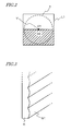
- FIG. 3 is a perspective view of the arrayed optical device K.
- a plurality of optical elements M 1 elongated in the horizontal direction are arranged in the vertical direction on one surface of the arrayed optical device K that is closer to the imaging device N.
- the cross section (in the vertical direction) of each optical element M 1 has a curved shape protruding toward the imaging device N.
- the arrayed optical device K has a lenticular lens configuration.
- the arrayed optical device K is arranged in the vicinity of the focal point of the lens optical system L, and is arranged at a position at a predetermined distance from the imaging surface Ni.
- FIG. 4( a ) is an enlarged view of the arrayed optical device K and the imaging device N shown in FIG. 1
- FIG. 4( b ) is a diagram showing the positional relationship between the arrayed optical device K and pixels on the imaging device N.
- the arrayed optical device K is arranged so that the surface on which the optical elements M 1 are formed faces the imaging surface Ni.
- the pixels P are arranged in a matrix pattern on the imaging surface Ni.
- the pixels P can be grouped into pixels P 1 and pixels P 2 .
- the pixels P 1 and the pixels P 2 are arranged in rows in the horizontal direction (row direction). In the vertical direction (column direction), the pixels P 1 and P 2 are arranged alternating with each other.
- the arrayed optical device K is arranged so that each optical element M 1 thereof corresponds to two rows of pixels including one row or pixels P 1 and one row of pixels P 2 on the imaging surface Ni.
- Microlenses Ms are provided on the imaging surface Ni so as to cover the surface of the pixels P 1 and P 2 .
- the arrayed optical device K is designed so that the majority of the light beam (the light beam B 1 represented by solid lines in FIG. 1 ) having passed through the optical area D 1 on the optical device L 1 (shown in FIG. 1 and FIG. 2 ) arrives at the pixels P 1 on the imaging surface Ni, and the majority of the light beam (the light beam B 2 represented by broken lines in FIG. 1 ) having passed through the optical area D 2 arrives at the pixels P 2 on the imaging surface Ni.
- the configuration described above is realized by appropriately setting parameters such as the refractive index of the arrayed optical device K, the distance from the imaging surface Ni, and the radius of curvature at the surface of the optical element M 1 .
- the angle of a light beam at the focal point is determined by the position of the light beam passing through the stop and the angle thereof with respect to the optical axis.
- the arrayed optical device has a function of differentiating the exit direction depending on the incident angle of the light beam. Therefore, by arranging the optical areas D 1 and D 2 in the vicinity of the stop and arranging the arrayed optical device K in the vicinity of the focal point as described above, the light beams B 1 and B 2 having passed through the respective optical areas can be separately guided to the pixels P 1 and P 2 , respectively.
- the imaging optical system is an image-side telecentric optical system, since light beams passing through the stop are parallel, the angle of a light beam at the focal point is uniquely determined by the position of the light beam passing through the stop.
- the pixels P 1 and the pixels P 2 generate image information corresponding to light of different wavelength bands from each other. That is, the imaging apparatus A is capable of obtaining a plurality of image information formed by light of different wavelength bands from each other through a single imaging operation using a single imaging optical system.
- the first optical area D 1 is an optical filter having characteristics such that visible light is transmitted therethrough as light of the first wavelength band while near infrared light is substantially blocked.
- the second optical area D 2 is an optical filter having characteristics such that visible light is substantially blocked while near infrared light is transmitted therethrough as light of the second wavelength band.
- the first optical area D 1 is an optical filter having characteristics such that visible light is transmitted therethrough as light of the first wavelength band while near ultraviolet light is substantially blocked.
- the second optical area D 2 is an optical filter having characteristics such that visible light is substantially blocked while near ultraviolet light is transmitted therethrough as light of the second wavelength band.
- the first optical area D 1 is an optical filter that transmits therethrough light of a predetermined wavelength band width
- the second optical area D 2 is an optical filter that transmits therethrough light of a narrower band width than the predetermined wavelength band width. That is, the width of the first wavelength band is made narrower than the width of the second wavelength band.
- the second wavelength band may or may not be included in the first wavelength band.
- a light source having spectral radiation characteristics including the first and second wavelength bands it is preferred to provide one type of a light source having spectral radiation characteristics including the first and second wavelength bands, or a plurality of types of light sources having spectral radiation characteristics corresponding respectively to the first and second wavelength bands.
- a lesion it is possible to easily distinguish a lesion by displaying on a monitor the image obtained with a wide band and the image obtained with a narrow band in different colors from each other.
- the pixel value is missing for every other pixel in the y direction. Therefore, the pixel value of the pixel for which it is missing may be generated by interpolation with pixel values of pixels adjacent thereto in the y direction, or pixel values in the x direction may be added together in groups of two pixels.
- a configuration may be used where the aspect ratio between the x direction and the y direction of each pixel of the imaging device is 2:1. With such a configuration, the interpolation process or the addition process as described above will be unnecessary.
- Embodiment 2 is different from Embodiment 1 in that the area of the optical device L 1 is divided in three.
- Embodiment 1 what is substantially the same as Embodiment 1 will not be described in detail.
- FIG. 5 is a schematic diagram showing the imaging apparatus A of Embodiment 2.
- the light beam B 1 is a light beam passing through the optical area D 1 on the optical device L 1
- the light beam B 2 is a light beam passing through the optical area D 2 on the optical device L 1
- a light beam B 3 is a light beam passing through the optical area D 3 on the optical device L 1 .
- the light beams B 1 , B 2 and B 3 pass through the stop S, the optical device L 1 , the lens L 2 and the arrayed optical device K in this order to arrive at the imaging surface Ni (shown in FIG. 7 , etc.) on the imaging device N.
- FIG. 6 is a front view of the optical device L 1 as seen from the object side, and the optical areas D 1 , D 2 and D 3 are formed by three-fold division in the up-down direction in a plane vertical to the optical axis V.
- the wavelength bands of light passing through different optical areas are different from each other.
- FIG. 7( a ) is an enlarged view of the arrayed optical device K and the imaging device N shown in FIG. 5
- FIG. 7( b ) is a diagram showing the positional relationship between the arrayed optical device K and pixels on the imaging device N.
- the arrayed optical device K is arranged so that the surface on which the optical elements M 1 are formed faces the imaging surface Ni.
- the pixels P are arranged in a matrix pattern on the imaging surface Ni.
- the pixels P can be grouped into pixels P 1 , pixels P 2 , and pixels P 3 .
- the pixels P 1 , the pixels P 2 and the pixels P 3 are arranged in rows in the horizontal direction (row direction). In the vertical direction (column direction), the pixels P 1 , P 2 and P 3 are arranged alternating with one another.
- the arrayed optical device K is arranged so that each optical element M 1 thereof corresponds to three rows of pixels including one row of pixels P 1 , one row of pixels P 2 and one row of pixels P 3 on the imaging surface Ni.
- Microlenses Ms are provided on the imaging surface Ni so as to cover the surface of the pixels P 1 , P 2 and P 3 .
- the arrayed optical device K is designed so that the majority of the light beam B 1 (the light beam B 1 represented by dotted lines in FIG. 5 ) having passed through the optical area D 1 on the optical device L 1 (shown in FIG. 5 and FIG. 6 ) arrives at the pixels P 1 on the imaging surface Ni, the majority of the light beam (the light beam B 2 represented by solid lines in FIG. 5 ) having passed through the optical area D 2 arrives at the pixels P 2 on the imaging surface Ni, and the majority of the light beam (the light beam B 3 represented by broken lines in FIG. 5 ) having passed through the optical area D 3 arrives at the pixels P 3 on the imaging surface Ni.
- the configuration described above is realized by appropriately setting parameters such as the refractive index of the arrayed optical device K, the distance from the imaging surface Ni, and the radius of curvature at the surface of the optical element M 1 .
- the pixels P 1 , the pixels P 2 and the pixels P 3 generate image information corresponding to light of different wavelength bands from each other. That is, the imaging apparatus A is capable of obtaining a plurality of image information formed by light of different wavelength bands from each other through a single imaging operation using a single imaging optical system.
- Embodiment 1 is a structure with which images of two different wavelength bands are obtained simultaneously
- Embodiment 2 is capable of simultaneously obtaining images of three different wavelength bands.
- the first optical area D 1 is a blue color filter that transmits therethrough light of the blue band while substantially blocking colors of non-blue bands.
- the second optical area D 2 is a green color filter that transmits therethrough light of the green band while substantially blocking colors of non-green bands.
- the third optical area D 3 is a red color filter that transmits therethrough light of the red band while substantially blocking colors of non-red bands.
- the pixel value is missing for every third pixel in the y direction.
- the pixel value of the pixel for which it is missing may be generated by interpolation with pixel values of pixels adjacent thereto in the y direction, or pixel values in the x direction may be added together in groups of three pixels.
- a configuration may be used where the aspect ratio between the x direction and the y direction of each pixel of the imaging device is 3:1. With such a configuration, the interpolation process or the addition process as described above will be unnecessary.
- Embodiment 3 is different from Embodiment 1 in that the area of the optical device L 1 of FIG. 1 is divided in four, and that the arrayed optical device is switched from a lenticular to a microlens.
- Embodiment 1 what is substantially the same as Embodiment 1 will not be described in detail.
- FIG. 8 is a front view of the optical device L 1 as seen from the object side, and the optical areas D 1 , D 2 , D 3 and D 4 are formed by four-fold division in the up-down direction and the left-right direction in a plane vertical to the optical axis V with the optical axis V being the center of the boundary.
- the wavelength bands of light passing through different optical areas are different from each other.
- FIG. 9 is a perspective view of the arrayed optical device K.
- Optical elements M 2 are arranged in a lattice pattern on one surface of the arrayed optical device K that is closer to the imaging device N.
- the cross sections (the cross section in the vertical direction and the cross section in the horizontal direction) of each optical element M 2 has a curved shape, and each optical element M 2 is protruding toward the imaging device N.
- the optical elements M 2 are microlenses
- the arrayed optical device K is a microlens array.
- FIG. 10( a ) is an enlarged view of the arrayed optical device K and the imaging device N
- FIG. 10( b ) is a diagram showing the positional relationship between the arrayed optical device K and pixels on the imaging device N.
- the arrayed optical device K is arranged so that the surface on which the optical elements M 2 are formed faces the imaging surface Ni.
- the pixels P are arranged in a matrix pattern on the imaging surface Ni.
- the pixels P can be grouped into pixels P 1 , pixels P 2 , pixels P 3 and pixels P 4 .
- the arrayed optical device K is arranged in the vicinity of the focal point of the lens optical system L, and is arranged at a position at a predetermined distance from the imaging surface Ni.
- Microlenses Ms are provided on the imaging surface Ni so as to cover the surface of the pixels P 1 , P 2 , P 3 and P 4 .
- the arrayed optical device K is arranged so that the surface on which the optical elements M 2 are formed faces the imaging surface Ni.
- the arrayed optical device K is arranged so that each optical element M 2 thereof corresponds to two rows and two columns, i.e., four, of pixels P 1 -P 4 on the imaging surface Ni.
- the arrayed optical device K is designed so that the majority of the light beam having passed through the optical areas D 1 , D 2 , D 3 and D 4 on the optical device L 1 arrive at the pixel P 1 , the pixel P 2 , the pixel P 3 and the pixel P 4 , respectively, on the imaging surface Ni.
- the configuration described above is realized by appropriately setting parameters such as the refractive index of the arrayed optical device K, the distance from the imaging surface Ni, and the radius of curvature at the surface of the optical element M 1 .
- the pixels P 1 , the pixels P 2 , the pixels P 3 and the pixels P 4 generate image information corresponding to light of different wavelength bands from each other. That is, the imaging apparatus A is capable of obtaining a plurality of image information formed by light of different wavelength bands through a single imaging operation using a single imaging optical system.
- Embodiment 1 and Embodiment 2 are structures with which images of two and three wavelength bands, respectively, are obtained simultaneously
- Embodiment 3 is capable of simultaneously obtaining images of four different wavelength bands.
- the configuration further includes a near infrared light filter that substantially blocks visible light including blue, green and red and transmits therethrough near infrared light.
- a near infrared light filter that substantially blocks visible light including blue, green and red and transmits therethrough near infrared light.
- the configuration further includes a near ultraviolet light filter that substantially blocks visible light including blue, green and red and transmits therethrough near ultraviolet light.
- a near ultraviolet light filter that substantially blocks visible light including blue, green and red and transmits therethrough near ultraviolet light.
- the configuration further includes a filter that transmits therethrough only a wavelength band of a narrower band width than the band widths of the spectral transmittance characteristics of the blue, green and red color filters.
- a filter that transmits therethrough only a wavelength band of a narrower band width than the band widths of the spectral transmittance characteristics of the blue, green and red color filters.
- the light source may include a white light source and a light source having spectral radiation characteristics including the narrow band.
- the pixel value is missing for every other pixel in the x direction and in the y direction. Therefore, the pixel value of the pixel for which it is missing may be generated by interpolation with pixel values of pixels adjacent thereto in the x direction and in the y direction.
- Two of the four areas obtained by four-fold division that oppose each other with the optical axis interposed therebetween may be color filters of the same green color. With such a configuration, the number of green pixels increases, and it is therefore possible to improve the resolution of the green image component.
- Embodiment 4 is different from Embodiment 1 in that the first optical area D 1 and the second optical area D 2 are each arranged in two separate parts with the optical axis interposed therebetween, and that the arrayed optical device is switched from a lenticular to a microlens.
- the first optical area D 1 and the second optical area D 2 are each arranged in two separate parts with the optical axis interposed therebetween, and that the arrayed optical device is switched from a lenticular to a microlens.
- FIG. 11( a ) is a front view of the optical device L 1 as seen from the object side, and the optical areas D 1 and D 2 are each arranged in two separate parts opposing each other in an axial symmetry direction with the optical axis V being the center so that the centroid thereof is the optical axis position.
- FIG. 11( b ) is a diagram showing the positional relationship between the arrayed optical device N and pixels on the imaging device N.
- light beams having passed through the optical area D 1 arrive at odd-numbered row/odd-numbered column positions and at even-numbered row/even-numbered column positions, and therefore the odd-numbered row/odd-numbered column positions and the even-numbered row/even-numbered column positions are added together to generate an image corresponding to the first wavelength band.
- Light beams having passed through the optical area D 2 arrive at even-numbered row/odd-numbered column positions and odd-numbered row/even-numbered column positions, and therefore the even-numbered row/odd-numbered column positions and the odd-numbered row/even-numbered column positions are added together to generate an image corresponding to the second wavelength band.
- the first optical area D 1 and the second optical area D 2 are areas obtained by two-fold division of the optical device L 1 in the up-down direction in a plane vertical to the optical axis. Therefore, the spot centroids on the image plane of light having passed through different optical areas may vary depending on the object distance, thereby causing parallax.
- FIG. 12 shows ray diagrams for different object distances in Embodiment 1, and diagrams illustrating point images and changes in centroids thereof.
- FIGS. 12( a 1 ), ( b 1 ) and ( c 1 ) show ray diagrams for different object distances.
- FIG. 12( a 1 ) is a ray diagram for a case where the object point O is at the greatest distance from the optical system
- FIG. 12( c 1 ) is for a case where the object point O is at the least distance
- FIG. 12( b 1 ) is for a case where the object point O is at a distance between that of ( a 1 ) and that of ( c 1 ).
- FIGS. 12 shows ray diagrams for different object distances in Embodiment 1, and diagrams illustrating point images and changes in centroids thereof.
- FIGS. 12( a 1 ), ( b 1 ) and ( c 1 ) show ray diagrams for different object distances.
- FIG. 12( a 2 ) and ( a 3 ), ( b 2 ) and ( b 3 ), and ( c 2 ) and ( c 3 ) show the point images (shown as semicircles) that are imaged through lenticulars and the centroids thereof (shown as black dots), corresponding to the object distances of (a 1 ), (b 1 ) and (c 1 ) of FIG. 12 , respectively.
- the point images are shown schematically as images obtained by interpolating the image information (a 2 , b 2 , c 2 ) extracted for each odd-numbered column and the pixel information (a 3 , b 3 , c 3 ) extracted for each even-numbered column for pixel values that are missing for every other pixel in the y direction.
- the point images of the images are two semicircular shapes obtained by dividing a single circle in two.
- the spot diameter increases as the object point O comes closer. Therefore, the inter-centroid distance d between the point images of the images increases as the object comes closer.
- the inter-centroid distance d is not desirable because it results in a parallax.
- the optical areas D 1 and D 2 are arranged to be separated from each other in an axial symmetry direction about the optical axis so that the centroid thereof is the optical axis position.
- the centroids of point images formed by light having passed through the optical areas D 1 and D 2 are also present at the optical axis position. Therefore, the inter-centroid distance d between point images does not vary even when the object distance varies.
- FIG. 13 shows diagrams illustrating point images and centroids thereof for different object distances.
- ( a 1 ) and ( a 2 ), ( b 1 ) and ( b 2 ), and ( c 1 ) and ( c 2 ) show the point images (shown in semicircles) that are imaged through lenticulars and the centroids thereof (black dots), corresponding to the object distances of (a 1 ), (b 1 ) and (c 1 ) of FIG. 12 , respectively.
- the point images schematically show image information (a 1 , b 1 , c 1 ) obtained by adding together the odd-numbered row/odd-numbered column positions and the even-numbered row/even-numbered column positions, and image information (a 2 , b 2 , c 2 ) obtained by adding together the even-numbered row/odd-numbered column positions and the odd-numbered row/even-numbered column positions.
- Embodiment 4 when the obtained image is divided into an image obtained by adding together the odd-numbered row/odd-numbered column positions and the even-numbered row/even-numbered column positions and an image obtained by adding together the even-numbered row/odd-numbered column positions and the odd-numbered row/even-numbered column positions, the point images of the images are fan shapes opposing each other in an axial symmetry direction about the optical axis. Since the centroids of these point image coincide with each other, the inter-centroid distance d between the point images of the images does not vary even when the object distance varies.
- Embodiment 4 as the optical areas D 1 and D 2 are each arranged in separate parts opposing each other in an axial symmetry direction about the optical axis so that the centroid thereof is the optical axis position, it is possible to ensure that a parallax does not occur between obtained images even when the object distance varies.
- Embodiment 5 is a configuration having two optical areas D 1 and D 2 as in Embodiment 1, and further assumes that the lens L 2 is a lens with axial chromatic aberration. With such a configuration, two areas with different levels of optical power are provided in a plane vertical to the optical axis in the vicinity of the stop so that the focus positions of light beams having passed through the optical areas D 1 and D 2 are substantially equal to each other.
- the embodiment is different from Embodiment 1 in this regard. Herein, what is substantially the same as Embodiment 1 will not be described in detail.
- one of the two areas with different levels of optical power transmits therethrough light that passes through the first optical area D 1 .
- the other area transmits therethrough light that passes through the second optical area D 2 .
- the optical areas D 1 and D 2 and the two areas with different levels of optical power may be formed on the same device or formed on different devices.
- FIG. 14( a ) is a diagram schematically showing a ray diagram in Embodiment 1 in a case where the lens L 2 is a lens that has axial chromatic aberration due to the wavelength dispersion characteristics of the refractive index as does a single lens.
- a filter that transmits therethrough light of the first wavelength band is formed in the first optical area D 1
- a filter that transmits therethrough light of the second wavelength band, relatively longer than the first wavelength band is formed in the second optical area D 2 .
- the lens L 2 is a lens that has axial chromatic aberration due to the wavelength dispersion characteristics of the refractive index, as does a single lens, for example, light having a longer wavelength is focused farther away from the lens. Therefore, if the settings are such that light beams having passed through the optical area D 1 are focused on the imaging surface Ni as shown in FIG. 14( a ), light beams having passed through the optical area D 2 will not yet be focused on the imaging surface Ni.
- FIG. 14( b ) is a diagram schematically showing a ray diagram for an imaging apparatus of Embodiment 5.
- a lens surface with such optical power that light beams of the wavelength band of second spectral transmittance characteristics will focus on the imaging surface is formed in the second optical area D 2 of the optical device L 1 . Therefore, light beams having passed through the first optical area D 1 and light beams having passed through the second optical area D 2 are both focused on the imaging surface Ni.
- the focus position of light passing through the first optical area D 1 and the focus position of light passing through the second optical area D 2 are brought closer to each other, as compared with a case where the first optical area D 1 and the second optical area D 2 have an equal level of optical power.
- the optical axis V′ of the optical on one side of the optical area D 2 of the optical device L 1 that is closer to the stop S has eccentricity as opposed to the optical axis V of the lens optical system, but since the optical power is very small as compared with the optical power of the lens L 2 , there is little deterioration of imaging performance.
- FIGS. 15( a ) and ( b ) are perspective views of the optical device L 1 shown in FIG. 14( b ).
- a filter having first spectral transmittance characteristics is formed on the first optical area D 1
- a filter having second spectral transmittance characteristics is formed on the second optical area D 2 , which is the lens surface.
- the lens surface is formed across the entire areas obtained by dividing the optical device L 1 in two. Therefore, there is a step between the first optical area, which is a plane, and the second optical area D 2 , which is a lens surface.
- the stop S preferably has a configuration in which a light-blocking area is provided as shown in FIGS. 16( a ) and ( b ).
- a lens surface is formed in a portion of an area obtained by dividing the optical device L 1 in two, to obtain the optical area D 2 .
- This configuration requires a configuration where a light-blocking area is provided as shown in FIG. 16( c ) so as to correspond to the optical areas D 1 and D 2 .
- FIGS. 17( a ) and ( b ) are diagrams showing other embodiments of Embodiment 5. While the optical axis V′ of the surface on one side of the optical area D 2 of the optical device L 1 that is closer to the stop S is different from the optical axis V of the lens optical system in FIG. 14( b ), the optical axis of the surface on one side of the optical area D 2 of the optical device L 1 that is closer to the stop S is the same as the optical axis of the lens L 2 in FIG. 17( a ).
- FIG. 18 is a perspective view of the optical device L 1 shown in FIG. 17( a ). With such a configuration, the eccentricity of the optical axis of the lens surface of the optical area D 2 of the optical device L 1 is eliminated, and it is possible to eliminate the deterioration of imaging performance due to eccentricity.
- FIG. 17( b ) is an example in which a separate lens is provided on the optical device L 1 , as opposed to FIG. 17( a ).
- the optical device L 1 on which filters of different spectral transmittance characteristics are formed is arranged on the object side in the vicinity of the stop, and an optical device L 1 ′ is arranged on the object side in the vicinity of the stop.
- Each of the optical devices L 1 and L 1 ′ has the first optical area D 1 and the second optical area D 2 .
- the second optical area D 2 of the optical device L 1 ′ has a lens surface.
- the element forming a filter and the element forming a lens may be separate from each other.
- the positions of L 1 and L 1 ′ may be switched around with respect to the stop.
- the lens L 2 is a lens, such as a single lens, whose axial chromatic aberration is not corrected, the axial chromatic aberration can be reduced by providing two areas having different levels of optical power from each other in a plane vertical to the optical axis.
- Embodiment 6 is a configuration having three optical areas D 1 , D 2 and D 3 as in Embodiment 2, and further assumes that the lens L 2 is a lens with axial chromatic aberration. With such a configuration, three areas with different levels of optical power are provided in a plane vertical to the optical axis in the vicinity of the stop so that the focus positions of light beams having passed through the optical areas D 1 and D 2 are substantially equal to each other.
- the embodiment is different from Embodiment 5 in this regard. Herein, what is substantially the same as Embodiment 5 will not be described in detail.
- FIGS. 19( a ), ( b ) and ( c ) are perspective views showing the optical device L 1 of Embodiment 6 where the optical area is divided in three.
- the stop S has configurations shown in FIGS. 20( a ), ( b ) and ( c ), similar to Embodiment 5.
- Embodiment 6 even if a lens, such as a single lens, whose axial chromatic aberration is not corrected is used, it is possible to reduce the axial chromatic aberration by providing three areas having different levels of optical power in a plane vertical to the optical axis.
- Embodiment 7 is a configuration having four optical areas D 1 , D 2 , D 3 and D 4 as in Embodiment 3, and further assumes that the lens L 2 is a lens with axial chromatic aberration. With such a configuration, four areas with different levels of optical power are provided in a plane vertical to the optical axis in the vicinity of the stop so that the focus positions of light beams having passed through the optical areas D 1 and D 2 are substantially equal to each other.
- the embodiment is different from Embodiment 5 in this regard. Herein, what is substantially the same as Embodiment 5 will not be described in detail.
- FIGS. 21( a ), ( b ) and ( c ) are perspective views showing the optical device L 1 of Embodiment 7 where the optical area is divided in four.
- the stop S has configurations shown in FIG. 22( a ), ( b ) and ( c ), similar to Embodiment 5.
- Embodiment 7 even if a lens, such as a single lens, whose axial chromatic aberration is not corrected is used, it is possible to reduce the axial chromatic aberration by providing four areas having different levels of optical power in a plane vertical to the optical axis.
- Embodiment 8 is different from Embodiments 1-7 in that a lenticular lens or a microlens array is formed on the imaging surface.
- a lenticular lens or a microlens array is formed on the imaging surface.
- FIGS. 23( a ) and ( b ) are enlarged views of the arrayed optical device K and the imaging device N.
- a lenticular lens (or a microlens array) Md is formed on the imaging surface Ni of the imaging device N.
- the pixels P are arranged in a matrix pattern, as in Embodiment 1, etc., on the imaging surface Ni.
- a single lenticular lens optical element or a single microlens corresponds to a plurality of pixels P.
- light beams having passed through different areas of the optical device L 1 can be guided to different pixels.
- FIG. 23( b ) is a diagram showing a variation of the present embodiment. In the configuration shown in FIG.
- the microlenses Ms are formed on the imaging surface Ni so as to cover the pixels P, and the arrayed optical device is layered on the surface of the microlenses Ms.
- FIG. 23( b ) it is possible to increase the light-condensing efficiency as compared with that of the configuration of FIG. 23( a ).
- the alignment between the arrayed optical device and the imaging device is difficult.
- the alignment can be done in the wafer process, thereby making the alignment easier and improving the alignment precision.
- Embodiments 1-8 are directed to configurations where the optical area is divided in two, three, or four, the number of division may be more.
- the lens L 2 is a single lens, it may be a plurality of groups of lenses or a plurality of lenses.
- the optical area is arranged on one surface of the optical device L 1 that is closer to the object
- the optical area may be arranged on one surface of the optical device L 1 that is closer to the image.
- the optical device L 1 is arranged on the image side with respect to the position of the stop, it may be arranged on the object side with respect to the position of the stop. In this case, it is preferred that the optical area is arranged on the image side of the optical device L 1 as it is then closer to the stop.
- the lens surface provided on the element which is different from the optical device L 1 or the optical device L 1 , is arranged on the object-side surface of the element in Embodiments 4, 5 and 6, it may be arranged on the image-side surface of the element.
- a plurality of color filters may be layered on one another.
- a dielectric multi-layer film filter and an absorption-type filter having different spectral transmittance characteristics may be layered together, or a dielectric multi-layer film may be formed on the absorption-type filter.
- an image-side non-telecentric optical system may be used, or an image-side telecentric optical system may be used.
- Many of the lenses used in imaging devices such as cameras use a non-telecentric optical system on the image side.
- the primary light beam is incident slantly on the arrayed optical device K if the angle of view changes.
- FIG. 24( a ) is an enlarged view showing the vicinity the imaging section outside the optical axis.
- FIG. 24( a ) shows only the light beams, of all the light passing through the arrayed optical device K, that pass through one optical area. As shown in FIG.
- the lens optical system L is an image-side non-telecentric optical system
- light is likely to leak to adjacent pixels, thereby causing crosstalk.
- the amount of offset ⁇ may be set in accordance with the angle of incidence of the light beam on the imaging surface.
- An image-side telecentric optical system may be used for the lens optical system L of an embodiment of the present invention.
- the primary light beam is incident on the arrayed optical device K with a value close to 0 degree even if the angle of view changes, and it is therefore possible to reduce the crosstalk across the entire imaging area.
- each microlens optical element has a shape that is rotationally symmetric with respect to the optical axis of the microlens.
- a method for manufacturing a microlens there is a method in which a resist is patterned into a rectangular shape, and the curved surface of the lens is formed by heat treatment.
- a perspective view of such microlenses is as shown in FIG. 25( a 1 ).
- the contour lines of the microlens of FIG. 25( a 1 ) are as shown in FIG. 25( a 2 ), and the radius of curvature in a vertical/horizontal direction and that in a diagonal direction are different from each other.
- FIG. 25( a 1 ) The contour lines of the microlens of FIG. 25( a 1 ) are as shown in FIG. 25( a 2 ), and the radius of curvature in a vertical/horizontal direction and that in a diagonal direction are different from each other.
- FIG. 25( a 3 ) shows the results of light beam tracking simulation in a case where the microlens shown in FIGS. 25( a 1 ) and ( a 2 ) is used as the arrayed optical device of the present invention.
- FIG. 25( a 3 ) only shows light beams, of all the light passing through the arrayed optical device K, that pass through one optical area. With such a microlens that is not rotationally asymmetric, light leaks to adjacent pixels, causing crosstalk.
- a perspective view of microlenses having a rotationally symmetric shape is as shown in FIG. 25( b 1 ).
- the contour lines of the microlens of FIG. 25( b 1 ) are as shown in FIG.
- FIG. 25( b 2 ) shows the results of light beam tracking simulation in a case where the microlens shown in FIGS. 25( b 1 ) and ( b 2 ) is used as the arrayed optical device of the present invention.
- FIG. 25( b 3 ) only shows light beams, of all the light passing through the arrayed optical device K, that pass through one optical area. It can be that there is no such crosstalk as that shown in FIG. 25( a 3 ).
- Embodiments 5, 6 and 7 show examples in which a light-blocking area is provided in the stop at a position corresponding to the step portions in order to prevent unnecessary light passing through steps, since light beams passing through the vicinity of boundaries between different areas may cause crosstalk as described above, such a stop as shown in FIG. 16 , FIG. 20 and FIG. 22 may be provided in order to prevent crosstalk even if there is no step.
- the imaging device used in Embodiments 1-8 may be either a monochrome imaging device or a color imaging device.
- the width of the wavelength band of light passing through at least area of the optical device L 1 may be narrower than the width of the wavelength band of the color filter on the pixel at which the light beam having passed through the area arrives. Since a color imaging device is used for the imaging device, it is not necessary to provide a color filter in areas other than the at least one area of the optical device L 1 . With such a configuration, it is possible to obtain image information of a narrow band and to attenuate the component of the wavelength band caused by crosstalk because of the effect of the spectral transmittance characteristics of the color imaging device. Since it is not necessary to provide a color filter on the optical device L 1 except for the at least one area, it is possible to reduce the cost.
- Embodiments 1-8 are imaging apparatuses having the signal processing section C.
- An imaging apparatus of the present invention may not include such a signal processing section.
- processes performed by the signal processing section C may be performed by using a PC, or the like, external to the imaging apparatus. That is, the present invention may also be implemented by a system including an imaging apparatus having the lens optical system L, the arrayed optical device K and the imaging device N, and an external signal processing device.
- An imaging apparatus of the present invention is useful as an imaging apparatus such as a digital still camera or a digital video camera. It is also applicable to cameras for obtaining spectral images, such as on-vehicle cameras, security cameras, medical applications, e.g., endoscopes and capsule endoscopes, biometric authentication applications, microscopes, and astronomical telescopes.
Landscapes
- Physics & Mathematics (AREA)
- General Physics & Mathematics (AREA)
- Engineering & Computer Science (AREA)
- Optics & Photonics (AREA)
- Multimedia (AREA)
- Signal Processing (AREA)
- Power Engineering (AREA)
- Spectroscopy & Molecular Physics (AREA)
- Condensed Matter Physics & Semiconductors (AREA)
- Electromagnetism (AREA)
- Computer Hardware Design (AREA)
- Microelectronics & Electronic Packaging (AREA)
- Studio Devices (AREA)
- Color Television Image Signal Generators (AREA)
- Lenses (AREA)
- Transforming Light Signals Into Electric Signals (AREA)
Priority Applications (1)
| Application Number | Priority Date | Filing Date | Title |
|---|---|---|---|
| US14/189,190 US8854525B2 (en) | 2011-04-22 | 2014-02-25 | Imaging device, imaging system, and imaging method |
Applications Claiming Priority (5)
| Application Number | Priority Date | Filing Date | Title |
|---|---|---|---|
| JP2011-095742 | 2011-04-22 | ||
| JP2011095742 | 2011-04-22 | ||
| PCT/JP2011/006093 WO2012143983A1 (ja) | 2011-04-22 | 2011-10-31 | 撮像装置、撮像システム、及び撮像方法 |
| US201213519627A | 2012-06-28 | 2012-06-28 | |
| US14/189,190 US8854525B2 (en) | 2011-04-22 | 2014-02-25 | Imaging device, imaging system, and imaging method |
Related Parent Applications (2)
| Application Number | Title | Priority Date | Filing Date |
|---|---|---|---|
| PCT/JP2011/006093 Continuation WO2012143983A1 (ja) | 2011-04-22 | 2011-10-31 | 撮像装置、撮像システム、及び撮像方法 |
| US13/519,627 Continuation US8717483B2 (en) | 2011-04-22 | 2011-10-31 | Imaging device, imaging system, and imaging method |
Publications (2)
| Publication Number | Publication Date |
|---|---|
| US20140168490A1 US20140168490A1 (en) | 2014-06-19 |
| US8854525B2 true US8854525B2 (en) | 2014-10-07 |
Family
ID=47041137
Family Applications (1)
| Application Number | Title | Priority Date | Filing Date |
|---|---|---|---|
| US14/189,190 Active US8854525B2 (en) | 2011-04-22 | 2014-02-25 | Imaging device, imaging system, and imaging method |
Country Status (5)
| Country | Link |
|---|---|
| US (1) | US8854525B2 (de) |
| EP (1) | EP2536153B1 (de) |
| JP (1) | JP2012235472A (de) |
| CN (1) | CN102907102B (de) |
| WO (1) | WO2012143983A1 (de) |
Cited By (2)
| Publication number | Priority date | Publication date | Assignee | Title |
|---|---|---|---|---|
| US9110218B2 (en) * | 2012-03-21 | 2015-08-18 | Fujifilm Corporation | Imaging device |
| US11457202B2 (en) | 2018-10-03 | 2022-09-27 | Fujifilm Corporation | Imaging device |
Families Citing this family (20)
| Publication number | Priority date | Publication date | Assignee | Title |
|---|---|---|---|---|
| US9843740B2 (en) | 2013-02-13 | 2017-12-12 | Panasonic Intellectual Property Management Co., Ltd. | Multispectral imaging device and multispectral imaging method |
| WO2015004886A1 (ja) | 2013-07-12 | 2015-01-15 | パナソニックIpマネジメント株式会社 | 撮像装置 |
| WO2015015717A1 (ja) | 2013-07-30 | 2015-02-05 | パナソニックIpマネジメント株式会社 | 撮像装置、並びにそれを用いた撮像システム、電子ミラーシステムおよび測距装置 |
| JP6277695B2 (ja) * | 2013-12-03 | 2018-02-14 | 株式会社リコー | 撮像装置、調整装置および調整方法 |
| JP6151632B2 (ja) * | 2013-12-20 | 2017-06-21 | 富士フイルム株式会社 | 撮像モジュール及び撮像装置 |
| US9484196B2 (en) | 2014-02-25 | 2016-11-01 | Micron Technology, Inc. | Semiconductor structures including liners comprising alucone and related methods |
| US11223014B2 (en) | 2014-02-25 | 2022-01-11 | Micron Technology, Inc. | Semiconductor structures including liners comprising alucone and related methods |
| US9509893B2 (en) * | 2014-03-31 | 2016-11-29 | Panasonic Intellectual Property Management Co., Ltd. | Imaging device and analyzing apparatus using the imaging device |
| US10249819B2 (en) | 2014-04-03 | 2019-04-02 | Micron Technology, Inc. | Methods of forming semiconductor structures including multi-portion liners |
| JP6536877B2 (ja) | 2014-07-31 | 2019-07-03 | パナソニックIpマネジメント株式会社 | 撮像装置および撮像システム |
| US9661193B2 (en) | 2014-08-01 | 2017-05-23 | Panasonic Intellectual Property Management Co., Ltd. | Imaging apparatus and analyzing apparatus |
| DE102014217750A1 (de) * | 2014-09-04 | 2016-03-10 | Conti Temic Microelectronic Gmbh | Kamerasystem und Verfahren zur Umfelderfassung eines Fahrzeugs |
| WO2016098170A1 (ja) * | 2014-12-15 | 2016-06-23 | オリンパス株式会社 | 撮像装置およびカプセル型内視鏡 |
| US9904146B2 (en) * | 2015-10-29 | 2018-02-27 | GM Global Technology Operations LLC | Camera with positionable light shade |
| WO2017217053A1 (ja) * | 2016-06-17 | 2017-12-21 | シャープ株式会社 | 画像撮像装置およびフィルタ |
| WO2018211588A1 (ja) * | 2017-05-16 | 2018-11-22 | オリンパス株式会社 | 撮像装置、撮像方法及びプログラム |
| KR101965529B1 (ko) * | 2018-04-06 | 2019-04-03 | 한양대학교 산학협력단 | 양자점층을 포함하는 듀얼 이미지 센서 |
| CN112840643B (zh) | 2018-10-09 | 2022-01-14 | 富士胶片株式会社 | 摄像装置 |
| CN112087559B (zh) * | 2019-06-13 | 2021-11-30 | 华为技术有限公司 | 图像传感器、图像拍摄装置和方法 |
| CN114631057A (zh) * | 2019-10-30 | 2022-06-14 | 富士胶片株式会社 | 摄像装置、摄像光学系统及摄像方法 |
Citations (32)
| Publication number | Priority date | Publication date | Assignee | Title |
|---|---|---|---|---|
| US4230941A (en) | 1979-03-26 | 1980-10-28 | Honeywell Inc. | Corrector lens |
| US4318123A (en) | 1980-06-05 | 1982-03-02 | Rca Corporation | Solid-state, color-encoding television camera |
| GB2092330A (en) | 1980-12-22 | 1982-08-11 | Agfa Gevaert Ag | Improvements in and relating to colour photography |
| US5600486A (en) | 1995-01-30 | 1997-02-04 | Lockheed Missiles And Space Company, Inc. | Color separation microlens |
| JPH11344662A (ja) | 1998-06-02 | 1999-12-14 | Ricoh Co Ltd | 自動合焦装置 |
| JP2001174696A (ja) | 1999-12-15 | 2001-06-29 | Olympus Optical Co Ltd | カラー撮像装置 |
| US20010017649A1 (en) | 1999-02-25 | 2001-08-30 | Avi Yaron | Capsule |
| JP2002135796A (ja) | 2000-10-25 | 2002-05-10 | Canon Inc | 撮像装置 |
| JP2003523646A (ja) | 1999-02-25 | 2003-08-05 | ヴィジョンセンス リミテッド | 光学装置 |
| US20050073603A1 (en) | 2003-10-01 | 2005-04-07 | Digital Optics Corporation | Thin camera having sub-pixel resolution |
| US20050124858A1 (en) | 2003-09-01 | 2005-06-09 | Hirohiko Matsuzawa | Capsule type endoscope |
| US20060082726A1 (en) | 2004-09-27 | 2006-04-20 | Kowa Company Ltd. | Ophthalmic photography apparatus |
| US20060124833A1 (en) | 2004-12-10 | 2006-06-15 | Atsushi Toda | Method and apparatus for acquiring physical information, method for manufacturing semiconductor device including array of plurality of unit components for detecting physical quantity distribution, light-receiving device and manufacturing method therefor, and solid-state imaging device and manufacturing method therefor |
| JP2006190958A (ja) | 2004-12-10 | 2006-07-20 | Sony Corp | 物理情報取得方法および物理情報取得装置、複数の単位構成要素が配列されてなる物理量分布検知の半導体装置の製造方法 |
| WO2007044725A2 (en) | 2005-10-07 | 2007-04-19 | The Board Of Trustees Of The Leland Stanford Junior University | Microscopy arrangements and approaches |
| US7242478B1 (en) | 2003-12-05 | 2007-07-10 | Surface Optics Corporation | Spatially corrected full-cubed hyperspectral imager |
| JP2007520166A (ja) | 2004-01-26 | 2007-07-19 | ディジタル・オプティックス・コーポレイション | サブピクセル解像度を有する薄型カメラ |
| US7427742B2 (en) * | 2002-10-11 | 2008-09-23 | Cypress Semiconductor Corporation | Microlens for use with a solid-state image sensor and a non-telecentric taking lens |
| US7433042B1 (en) * | 2003-12-05 | 2008-10-07 | Surface Optics Corporation | Spatially corrected full-cubed hyperspectral imager |
| US20090027542A1 (en) | 2007-07-13 | 2009-01-29 | Sony Corporation | Image pickup apparatus |
| JP4253550B2 (ja) | 2003-09-01 | 2009-04-15 | オリンパス株式会社 | カプセル型内視鏡 |
| US20090135282A1 (en) | 2007-11-27 | 2009-05-28 | Commissariat A L'energie Atomique | Visible imaging device with a colour filter |
| JP2010212306A (ja) | 2009-03-06 | 2010-09-24 | Panasonic Corp | 固体撮像装置 |
| US20100267163A1 (en) | 2009-04-20 | 2010-10-21 | Bio-Rad Laboratories Inc. | Non-scanning spr system |
| US20100283863A1 (en) | 2009-05-11 | 2010-11-11 | Sony Corporation | Imaging device |
| US20100283884A1 (en) | 2009-05-08 | 2010-11-11 | Sony Corporation | Imaging device |
| US20100328780A1 (en) * | 2008-03-28 | 2010-12-30 | Contrast Optical Design And Engineering, Inc. | Whole Beam Image Splitting System |
| US20110073752A1 (en) | 2009-09-30 | 2011-03-31 | Kathrin Berkner | Adjustable Multimode Lightfield Imaging System |
| WO2012066741A1 (ja) | 2010-11-16 | 2012-05-24 | 株式会社ニコン | マルチバンドカメラ及びマルチバンド画像撮像方法 |
| US20120182438A1 (en) | 2011-01-17 | 2012-07-19 | Kathrin Berkner | Multi-imaging System with Interleaved Images |
| EP2495540A2 (de) | 2011-03-04 | 2012-09-05 | Ricoh Company, Ltd. | Design von Filtermodulen für öffnungskodierte Multiplex-Bildgebungssysteme |
| US8427548B2 (en) * | 2008-06-18 | 2013-04-23 | Samsung Electronics Co., Ltd. | Apparatus and method for capturing digital images |
Family Cites Families (1)
| Publication number | Priority date | Publication date | Assignee | Title |
|---|---|---|---|---|
| CN100452414C (zh) * | 2004-12-10 | 2009-01-14 | 索尼株式会社 | 获取物理信息的方法、装置及装置的制造方法 |
-
2011
- 2011-10-31 CN CN201180005162.9A patent/CN102907102B/zh active Active
- 2011-10-31 WO PCT/JP2011/006093 patent/WO2012143983A1/ja active Application Filing
- 2011-10-31 EP EP11852202.8A patent/EP2536153B1/de active Active
-
2012
- 2012-05-16 JP JP2012112504A patent/JP2012235472A/ja active Pending
-
2014
- 2014-02-25 US US14/189,190 patent/US8854525B2/en active Active
Patent Citations (36)
| Publication number | Priority date | Publication date | Assignee | Title |
|---|---|---|---|---|
| US4230941A (en) | 1979-03-26 | 1980-10-28 | Honeywell Inc. | Corrector lens |
| US4318123A (en) | 1980-06-05 | 1982-03-02 | Rca Corporation | Solid-state, color-encoding television camera |
| GB2092330A (en) | 1980-12-22 | 1982-08-11 | Agfa Gevaert Ag | Improvements in and relating to colour photography |
| JPS592012B2 (ja) | 1980-12-22 | 1984-01-17 | アグファ−ゲ−ヴェルト・アクチエンゲゼルシャフト | 写真装置 |
| US5600486A (en) | 1995-01-30 | 1997-02-04 | Lockheed Missiles And Space Company, Inc. | Color separation microlens |
| JPH11344662A (ja) | 1998-06-02 | 1999-12-14 | Ricoh Co Ltd | 自動合焦装置 |
| US20010017649A1 (en) | 1999-02-25 | 2001-08-30 | Avi Yaron | Capsule |
| JP2003523646A (ja) | 1999-02-25 | 2003-08-05 | ヴィジョンセンス リミテッド | 光学装置 |
| JP2001174696A (ja) | 1999-12-15 | 2001-06-29 | Olympus Optical Co Ltd | カラー撮像装置 |
| JP2002135796A (ja) | 2000-10-25 | 2002-05-10 | Canon Inc | 撮像装置 |
| US7427742B2 (en) * | 2002-10-11 | 2008-09-23 | Cypress Semiconductor Corporation | Microlens for use with a solid-state image sensor and a non-telecentric taking lens |
| US20050124858A1 (en) | 2003-09-01 | 2005-06-09 | Hirohiko Matsuzawa | Capsule type endoscope |
| JP4253550B2 (ja) | 2003-09-01 | 2009-04-15 | オリンパス株式会社 | カプセル型内視鏡 |
| US20050073603A1 (en) | 2003-10-01 | 2005-04-07 | Digital Optics Corporation | Thin camera having sub-pixel resolution |
| US7242478B1 (en) | 2003-12-05 | 2007-07-10 | Surface Optics Corporation | Spatially corrected full-cubed hyperspectral imager |
| US7433042B1 (en) * | 2003-12-05 | 2008-10-07 | Surface Optics Corporation | Spatially corrected full-cubed hyperspectral imager |
| JP2007520166A (ja) | 2004-01-26 | 2007-07-19 | ディジタル・オプティックス・コーポレイション | サブピクセル解像度を有する薄型カメラ |
| US20060082726A1 (en) | 2004-09-27 | 2006-04-20 | Kowa Company Ltd. | Ophthalmic photography apparatus |
| US20060124833A1 (en) | 2004-12-10 | 2006-06-15 | Atsushi Toda | Method and apparatus for acquiring physical information, method for manufacturing semiconductor device including array of plurality of unit components for detecting physical quantity distribution, light-receiving device and manufacturing method therefor, and solid-state imaging device and manufacturing method therefor |
| JP2006190958A (ja) | 2004-12-10 | 2006-07-20 | Sony Corp | 物理情報取得方法および物理情報取得装置、複数の単位構成要素が配列されてなる物理量分布検知の半導体装置の製造方法 |
| WO2007044725A2 (en) | 2005-10-07 | 2007-04-19 | The Board Of Trustees Of The Leland Stanford Junior University | Microscopy arrangements and approaches |
| US20080266655A1 (en) | 2005-10-07 | 2008-10-30 | Levoy Marc S | Microscopy Arrangements and Approaches |
| US20090027542A1 (en) | 2007-07-13 | 2009-01-29 | Sony Corporation | Image pickup apparatus |
| US20090135282A1 (en) | 2007-11-27 | 2009-05-28 | Commissariat A L'energie Atomique | Visible imaging device with a colour filter |
| EP2065743A1 (de) | 2007-11-27 | 2009-06-03 | Commissariat A L'energie Atomique | Bildgebungsvorrichtung mit Farbfilter |
| US20100328780A1 (en) * | 2008-03-28 | 2010-12-30 | Contrast Optical Design And Engineering, Inc. | Whole Beam Image Splitting System |
| US8427548B2 (en) * | 2008-06-18 | 2013-04-23 | Samsung Electronics Co., Ltd. | Apparatus and method for capturing digital images |
| JP2010212306A (ja) | 2009-03-06 | 2010-09-24 | Panasonic Corp | 固体撮像装置 |
| US20100267163A1 (en) | 2009-04-20 | 2010-10-21 | Bio-Rad Laboratories Inc. | Non-scanning spr system |
| US20100283884A1 (en) | 2009-05-08 | 2010-11-11 | Sony Corporation | Imaging device |
| US20100283863A1 (en) | 2009-05-11 | 2010-11-11 | Sony Corporation | Imaging device |
| US20110073752A1 (en) | 2009-09-30 | 2011-03-31 | Kathrin Berkner | Adjustable Multimode Lightfield Imaging System |
| WO2012066741A1 (ja) | 2010-11-16 | 2012-05-24 | 株式会社ニコン | マルチバンドカメラ及びマルチバンド画像撮像方法 |
| US20120182438A1 (en) | 2011-01-17 | 2012-07-19 | Kathrin Berkner | Multi-imaging System with Interleaved Images |
| EP2495540A2 (de) | 2011-03-04 | 2012-09-05 | Ricoh Company, Ltd. | Design von Filtermodulen für öffnungskodierte Multiplex-Bildgebungssysteme |
| US20120226480A1 (en) * | 2011-03-04 | 2012-09-06 | Ricoh Co., Ltd. | Design of Filter Modules for Aperture-coded, Multiplexed Imaging Systems |
Non-Patent Citations (5)
| Title |
|---|
| Co-pending U.S. Appl. No. 13/519,627, filed Jun. 28, 2012. |
| Form PCT/ISA/237 for corresponding International Application No. PCT/JP2011/006093 dated Jan. 17, 2012. |
| International Search Report for corresponding International Application No. PCT/JP2011/006093 mailed Jan. 17, 2012. |
| Official Communication for corresponding European Application No. 11 852 202.8 issued Jun. 16, 2014. |
| Supplementary European Search Report for corresponding European Application No. 11852202.8 dated Mar. 7, 2013. |
Cited By (2)
| Publication number | Priority date | Publication date | Assignee | Title |
|---|---|---|---|---|
| US9110218B2 (en) * | 2012-03-21 | 2015-08-18 | Fujifilm Corporation | Imaging device |
| US11457202B2 (en) | 2018-10-03 | 2022-09-27 | Fujifilm Corporation | Imaging device |
Also Published As
| Publication number | Publication date |
|---|---|
| EP2536153A1 (de) | 2012-12-19 |
| CN102907102A (zh) | 2013-01-30 |
| CN102907102B (zh) | 2015-04-01 |
| US20140168490A1 (en) | 2014-06-19 |
| EP2536153B1 (de) | 2016-04-13 |
| WO2012143983A1 (ja) | 2012-10-26 |
| EP2536153A4 (de) | 2013-07-31 |
| JP2012235472A (ja) | 2012-11-29 |
Similar Documents
| Publication | Publication Date | Title |
|---|---|---|
| US8854525B2 (en) | Imaging device, imaging system, and imaging method | |
| US8717483B2 (en) | Imaging device, imaging system, and imaging method | |
| US20230308781A1 (en) | Solid-state image pickup device and electronic apparatus | |
| JP6004235B2 (ja) | 撮像装置および撮像システム | |
| EP2083447B1 (de) | Bildaufnahmevorrichtung | |
| US9793308B2 (en) | Imager integrated circuit and stereoscopic image capture device | |
| JP6120508B2 (ja) | 撮像素子および撮像装置 | |
| US8836825B2 (en) | Imaging apparatus | |
| US20110157451A1 (en) | Imaging device | |
| JP2011515045A (ja) | 多視点のイメージ取得を備えたセンサー | |
| WO2013047111A1 (ja) | 撮像装置及び合焦用パラメータ値算出方法 | |
| US9099369B2 (en) | Solid-state image sensor | |
| JP5332423B2 (ja) | 撮像装置 | |
| CN103460703A (zh) | 彩色摄像元件、摄像装置及摄像程序 | |
| WO2013114895A1 (ja) | 撮像装置 | |
| US11930256B2 (en) | Imaging device, imaging optical system, and imaging method | |
| JP2012169673A (ja) | 固体撮像装置および電子機器 | |
| WO2013038595A1 (ja) | 撮像装置 | |
| JP6222949B2 (ja) | 撮像素子および撮像装置 | |
| JP5537618B2 (ja) | 撮像装置 | |
| JP2009182550A (ja) | カメラモジュール | |
| JP2005327921A (ja) | 固体撮像装置 | |
| JP6010922B2 (ja) | 撮像装置 | |
| Radl | Optimum pixel design for dispersive filtering |
Legal Events
| Date | Code | Title | Description |
|---|---|---|---|
| STCF | Information on status: patent grant |
Free format text: PATENTED CASE |
|
| MAFP | Maintenance fee payment |
Free format text: PAYMENT OF MAINTENANCE FEE, 4TH YEAR, LARGE ENTITY (ORIGINAL EVENT CODE: M1551) Year of fee payment: 4 |
|
| MAFP | Maintenance fee payment |
Free format text: PAYMENT OF MAINTENANCE FEE, 8TH YEAR, LARGE ENTITY (ORIGINAL EVENT CODE: M1552); ENTITY STATUS OF PATENT OWNER: LARGE ENTITY Year of fee payment: 8 |