US8779396B2 - Drawing apparatus, and method of manufacturing article - Google Patents
Drawing apparatus, and method of manufacturing article Download PDFInfo
- Publication number
- US8779396B2 US8779396B2 US13/705,754 US201213705754A US8779396B2 US 8779396 B2 US8779396 B2 US 8779396B2 US 201213705754 A US201213705754 A US 201213705754A US 8779396 B2 US8779396 B2 US 8779396B2
- Authority
- US
- United States
- Prior art keywords
- mark
- region
- data
- substrate
- information
- Prior art date
- Legal status (The legal status is an assumption and is not a legal conclusion. Google has not performed a legal analysis and makes no representation as to the accuracy of the status listed.)
- Expired - Fee Related
Links
Images


Classifications
-
- G—PHYSICS
- G21—NUCLEAR PHYSICS; NUCLEAR ENGINEERING
- G21K—TECHNIQUES FOR HANDLING PARTICLES OR IONISING RADIATION NOT OTHERWISE PROVIDED FOR; IRRADIATION DEVICES; GAMMA RAY OR X-RAY MICROSCOPES
- G21K5/00—Irradiation devices
- G21K5/10—Irradiation devices with provision for relative movement of beam source and object to be irradiated
-
- H—ELECTRICITY
- H01—ELECTRIC ELEMENTS
- H01J—ELECTRIC DISCHARGE TUBES OR DISCHARGE LAMPS
- H01J37/00—Discharge tubes with provision for introducing objects or material to be exposed to the discharge, e.g. for the purpose of examination or processing thereof
- H01J37/30—Electron-beam or ion-beam tubes for localised treatment of objects
- H01J37/317—Electron-beam or ion-beam tubes for localised treatment of objects for changing properties of the objects or for applying thin layers thereon, e.g. for ion implantation
- H01J37/3174—Particle-beam lithography, e.g. electron beam lithography
- H01J37/3177—Multi-beam, e.g. fly's eye, comb probe
-
- B—PERFORMING OPERATIONS; TRANSPORTING
- B82—NANOTECHNOLOGY
- B82Y—SPECIFIC USES OR APPLICATIONS OF NANOSTRUCTURES; MEASUREMENT OR ANALYSIS OF NANOSTRUCTURES; MANUFACTURE OR TREATMENT OF NANOSTRUCTURES
- B82Y10/00—Nanotechnology for information processing, storage or transmission, e.g. quantum computing or single electron logic
-
- B—PERFORMING OPERATIONS; TRANSPORTING
- B82—NANOTECHNOLOGY
- B82Y—SPECIFIC USES OR APPLICATIONS OF NANOSTRUCTURES; MEASUREMENT OR ANALYSIS OF NANOSTRUCTURES; MANUFACTURE OR TREATMENT OF NANOSTRUCTURES
- B82Y40/00—Manufacture or treatment of nanostructures
-
- H—ELECTRICITY
- H01—ELECTRIC ELEMENTS
- H01J—ELECTRIC DISCHARGE TUBES OR DISCHARGE LAMPS
- H01J37/00—Discharge tubes with provision for introducing objects or material to be exposed to the discharge, e.g. for the purpose of examination or processing thereof
- H01J37/30—Electron-beam or ion-beam tubes for localised treatment of objects
- H01J37/304—Controlling tubes by information coming from the objects or from the beam, e.g. correction signals
- H01J37/3045—Object or beam position registration
Definitions
- the present invention relates to a drawing apparatus, and a method of manufacturing an article.
- a charged particle beam drawing apparatus which draws a pattern on (transfers it onto) a substrate with a charged particle beam (electron beam) has been known.
- Charged particle beam drawing apparatuses are roughly classified into a single-beam drawing apparatus which performs drawing with one charged particle beam, and a multibeam drawing apparatus which performs drawing with a plurality of charged particle beams.
- a multibeam drawing apparatus is attracting a great deal of attention as an apparatus available for mass production because the throughput is expected to improve more than a single-beam drawing apparatus.
- a charged particle beam drawing apparatus deflects (scans) a charged particle beam along a design coordinate system set on a substrate, and controls ON/OFF of the irradiation (blanking) of the substrate with the charged particle beam, thereby drawing a pattern on the substrate.
- a charged particle beam drawing apparatus converts design data representing a pattern (circuit pattern) to be drawn on a substrate into drawing data, and controls ON/OFF of the irradiation of the substrate with a charged particle beam based on the drawing data, regardless of whether the charged particle beam drawing apparatus is of the single-beam or multibeam type.
- the design data is CAD data or vector data
- the drawing data is bitmap data.
- Japanese Patent Laid-Open No. 8-505003 proposes a technique of converting CAD data or vector data (design data) into bitmap data.
- the design data includes not only a pattern to be drawn on a substrate but also a mark such as an alignment mark or an inspection mark, so it is impossible to change the mark drawing position or drawing timing immediately before drawing a pattern.
- a mark such as an alignment mark or an inspection mark
- an alignment mark inspection mark
- the alignment error may increase.
- the present invention provides, for example, a drawing apparatus advantageous in terms of drawing of a mark.
- a drawing apparatus which performs drawing on a substrate with a charged particle beam based on drawing data generated from pattern data representing a circuit pattern to be drawn on the substrate, and mark data representing a mark to be drawn on the substrate, the apparatus including an obtaining unit configured to obtain information associated with a positioning accuracy of the charged particle beam relative to the substrate, a determination unit configured to determine a drawing region for the mark based on the obtained information, and a generation unit configured to generate the drawing data by combining the pattern data and the mark data such that the mark is drawn in the determined drawing region.
- FIG. 1 is a view showing the configuration of a drawing apparatus according to an aspect of the present invention.
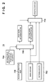
- FIG. 2 is a block diagram showing the basic configuration of a drawing data generation unit in the drawing apparatus shown in FIG. 1 .
- FIG. 3 is a block diagram showing the configuration of a drawing data generation unit in the first embodiment.
- FIG. 4 is a block diagram showing the configuration of a drawing data generation unit in the second embodiment.
- FIG. 5 is a block diagram showing the configuration of a drawing data generation unit in the third embodiment.
- FIG. 6 is a block diagram showing the configuration of a drawing data generation unit in the fourth embodiment.
- FIG. 7 is a block diagram showing the configuration of a drawing data generation unit in the fifth embodiment.
- FIG. 8 is a flowchart for explaining a process by a determination unit in updating mark region information.
- FIG. 9 is a view illustrating an example of mark region information managed by a management unit.
- FIG. 1 is a block diagram showing the configuration of a drawing apparatus 1 according to an aspect of the present invention.
- the drawing apparatus 1 serves as a lithography apparatus which draws a pattern on a substrate with a charged particle beam (electron beam).
- a charged particle beam electron beam
- the drawing apparatus 1 is implemented as a multibeam drawing apparatus in this embodiment, it may be implemented as a single-beam drawing apparatus.
- the drawing apparatus 1 includes a plurality of electron sources 10 a , 10 b , and 10 c , charged particle optical system 20 , deflector 30 , dynamic focus coil 40 , dynamic astigmatism coil 50 , substrate stage 60 , drawing data generation unit 70 , and control unit 80 .
- Each of the electron sources 10 a , 10 b , and 10 c includes, for example, an electron gun, and undergoes individual control of ON/OFF of the irradiation with a charged particle beam (electron beam).
- the charged particle optical system 20 guides the charged particle beams from the electron sources 10 a , 10 b , and 10 c , respectively, onto a substrate ST.
- the deflector 30 deflects (scans) the charged particle beams guided onto the substrate ST by the charged particle optical system 20 .
- the dynamic focus coil 40 corrects the focus positions of the charged particle beams which pass through the charged particle optical system 20 , in accordance with deflection aberrations generated in these charged particle beams upon the operation of the deflector 30 .
- the dynamic astigmatism coil 50 corrects the astigmatisms of the charged particle beams which pass through the charged particle optical system 20 , in accordance with deflection aberrations generated in these charged particle beams.
- the substrate stage 60 moves upon holding the substrate
- the electron sources 10 a , 10 b , and 10 c , charged particle optical system 20 , deflector 30 , dynamic focus coil 40 , dynamic astigmatism coil 50 , and substrate stage 60 constitute a drawing process unit.
- the drawing process unit performs a drawing process under the control of the control unit 80 .
- the drawing data generation unit 70 has a function of, for example, converting CAD data or vector data into bitmap data, and generates drawing data corresponding to a pattern to be drawn on the substrate ST.
- the drawing data generation unit 70 will be described in more detail later.
- the control unit 80 includes, for example, a CPU and memory and controls the overall drawing apparatus 1 (its operation). For example, the control unit 80 controls the drawing process unit (each unit constituting it) based on the drawing data generated by the drawing data generation unit 70 to scan the charged particle beams on the substrate ST, thereby drawing a pattern on the substrate ST.
- FIG. 2 is a block diagram showing the basic configuration of the drawing data generation unit 70 .
- the drawing data generation unit 70 includes a storage unit 702 , obtaining unit 704 , holding unit 706 , determination unit 708 , and generation unit 710 .
- the storage unit 702 stores CAD data or vector data as design data.
- the design data includes pattern data representing a circuit pattern to be drawn on a substrate, and mark data representing a mark (alignment mark or inspection mark) to be drawn on the substrate in order to measure or inspect the substrate.
- a circuit pattern and mark data are stored as one design data without distinction.
- the storage unit 702 stores, as independent data, pattern data PD representing a circuit pattern to be drawn on the substrate ST, and mark data MD representing marks to be drawn on the substrate ST.
- mark data MD mark data representing a mark to be drawn in a drawing region (at a drawing position) which need not be flexibly changed in accordance with the apparatus conditions because it requires low drawing position accuracy, or a mark to be drawn in a fixed region may partly serve as the pattern data PD.
- the obtaining unit 704 obtains information PI associated with the positioning accuracy of the charged particle beams relative to the substrate ST.
- the information PI includes at least one of, for example, surface shape information (flatness information) SI indicating the flatness of the substrate ST at each position, time information TI indicating the execution time of calibration of the drawing apparatus 1 , and environment information EI indicating the environment of the drawing apparatus 1 .
- the holding unit 706 holds region information MDR indicating a region in which a mark (for example, an alignment mark or an inspection mark) can be drawn on the substrate ST.
- the region in which a mark can be drawn means herein a region within which a mark can be drawn freely.
- the region information MDR may be arbitrarily set by the user, or automatically set by the drawing apparatus 1 based on the circuit pattern (pattern data PD) to be drawn on the substrate ST.
- the determination unit 708 determines the mark drawing region relative to a circuit pattern to be drawn on the substrate ST from the region indicated by the region information MDR held in the holding unit 706 , based on the information PI obtained by the obtaining unit 704 .
- the determination unit 708 analyzes the information PI and region information MDR to determine an optimum mark drawing region (drawing timing) on the substrate ST, and the mark shape and dimension.
- the determination unit 708 generates first mark information FMI indicating the determined mark drawing region, and second mark information SMI indicating the determined mark shape and dimension, and inputs them to the generation unit 710 .
- the determination unit 708 can arbitrarily determine the mark drawing region based on the information PI obtained by the obtaining unit 704 , independently of the region information MDR held in the holding unit 706 .
- the generation unit 710 combines the pattern data PD and mark data MD stored in the storage unit 702 so as to draw a mark in the drawing region determined by the determination unit 708 , thereby generating drawing data DD. More specifically, the generation unit 710 generates combined data by combining the pattern data PD and mark data MD based on the first mark information FMI and second mark information SMI, and converts the combined data into bitmap data, thereby generating drawing data DD.
- the drawing region (drawing position) and the drawing timing are integral, so the drawing timing is determined if the drawing region is determined, and vice versa. Hence, the drawing timing is determined to satisfy a required drawing region in some cases, while the drawing region is determined to satisfy a required drawing timing in other cases.
- certain amounts of pattern data and mark data are combined to generate drawing data before the start of drawing in some cases, while pattern data and mark data are combined in the order of drawing to sequentially generate drawing data in other cases.
- the second embodiment the case wherein a drawing region is determined to satisfy a required drawing timing
- pattern data and mark data are combined in the order of drawing to sequentially generate drawing data.
- certain amounts of pattern data and mark data can be combined to generate drawing data before the start of drawing, depending on the conditions involved.
- the drawing data generation unit 70 will be described in more detail below in each embodiment.
- FIG. 3 is a block diagram showing the configuration of a drawing data generation unit 70 in the first embodiment.
- an obtaining unit 704 obtains surface shape information SI indicating the flatness of the substrate ST at each position as information PI associated with the positioning accuracy of charged particle beams on the substrate ST.
- the focus positions in, for example, a region having dust adhered in it and a region with a rough surface shape on the substrate ST are considerably different from those in other regions. Therefore, the surface shape information SI can be obtained from a focus deviation within the substrate plane.
- a determination unit 708 determines, based on the surface shape information SI, the mark drawing region from a region in which the flatness falls within a tolerance (a region which satisfies a required flatness), for example, a region having no dust adhered in it within a region indicated by region information MDR held in a holding unit 706 . However, if the region indicated by the region information MDR includes no sufficient region which satisfies a required flatness, the determination unit 708 can change the mark shape and dimension. In other words, the determination unit 708 can determine the mark shape and dimension so as to draw a mark in a region which satisfies a required flatness. In general, the mark shape and dimension are integrally determined, so the mark shape changes with a change in mark dimension.
- the determination unit 708 displays an error (or warning) message for notifying to that effect on a display unit (not shown) of a drawing apparatus 1 , or records an error log in, for example, a memory of a control unit 80 .
- the determination unit 708 may determine, as a mark drawing region, the drawing region designated by default setting, independently of the region information MDR or the surface shape information SI.
- a drawing region in which a mark such as an alignment mark or an inspection mark is drawn can be determined (changed) in accordance with the flatness of the substrate ST, degradation in alignment accuracy and inspection accuracy can be suppressed (prevented). Also, in this embodiment, regardless of whether a multibeam or single-beam drawing apparatus is used, the drawing timing is uniquely determined in accordance with the mark drawing position as the mark drawing region is determined.
- FIG. 4 is a block diagram showing the configuration of a drawing data generation unit 70 in the second embodiment.
- the state of a drawing apparatus 1 is monitored in real time, and a mark such as an alignment mark or an inspection mark is drawn upon an interruption in accordance with the state of the drawing apparatus 1 . Therefore, pattern data PD is read out in the order of drawing, or is divided into minute regions and combined with mark data MD to generate drawing data DD upon an interruption.
- an obtaining unit 704 obtains time information TI indicating the execution time of calibration of the drawing apparatus 1 , and environment information EI indicating the environment of the drawing apparatus 1 .
- a determination unit 708 determines the mark drawing region by setting a mark drawing flag when the drawing conditions under which a mark is drawn are satisfied, based on the time information TI and environment information EI obtained by the obtaining unit 704 .
- the environment information EI includes, for example, temperature information indicating the temperature of a substrate ST.
- the determination unit 708 determines the mark drawing region (drawing timing) so as to draw a mark at the timing at which the temperature of the substrate ST reaches a predetermined temperature. In other words, the determination unit 708 determines the mark drawing region from a region indicated by region information MDR held in a holding unit 706 , based on the environment information EI so as to draw a mark at the timing at which the environment of the drawing apparatus 1 falls within a tolerance. This makes it possible to draw a pattern on the substrate ST free from the influence of a change in temperature of the substrate ST.
- the determination unit 708 determines the mark drawing region (drawing timing) so as to draw a mark immediately after the drawing apparatus 1 calibrated. In other words, the determination unit 708 determines the mark drawing region from the region indicated by the region information MDR held in the holding unit 706 , based on the time information TI, so as to draw a mark within a predetermined period after the execution time of calibration of the drawing apparatus 1 .
- the drawing timing at which a circuit pattern and a mark are drawn can be detected in advance, and then drawing data can be generated with a sufficient margin before a circuit pattern and a mark are drawn.
- drawing can be started after pattern data PD and mark data MD corresponding to one chip are combined to generate drawing data DD.
- mark drawing timing is uniquely determined in accordance with the environment information EI and time information TI in this embodiment, it may be changed for each mark drawing operation or for each type of mark.
- the mark drawing region (drawing timing) can be determined so as to draw a mark at the same timing as the timing at which a circuit pattern is drawn. More specifically, the mark drawing region is determined from a region, in which a mark can be drawn, so as to draw a mark at the timing at which a mark drawing flag is set, or at a timing as close to it as possible.
- the mark drawing region can be determined from a region, in which a mark can be drawn, so as to draw a mark at a timing as immediately after a mark drawing flag is set as possible.
- a substrate stage 60 must be moved in drawing a mark, so the mark drawing accuracy may become lower than in a multibeam drawing apparatus.
- the obtaining unit 704 can obtain surface shape information SI in addition to the environment information EI and time information TI.
- a region in which the flatness falls outside a tolerance may be excluded from the region indicated by the region information MDR held in the holding unit 706 , based on the surface shape information SI, before the mark drawing region is determined.
- the mark drawing region can be efficiently determined based on the environment information EI and time information TI.
- the determination unit 708 can change the mark shape and dimension.
- the determination unit 708 displays an error (or warning) message for notifying to that effect on a display unit (not shown) of the drawing apparatus 1 , or records an error log in, for example, a memory of a control unit 80 .
- the determination unit 708 may determine, as a mark drawing region, the drawing region designated by default setting, independently of the environment information EI or the time information TI.
- a drawing region in which a mark such as an alignment mark or an inspection mark is drawn can be determined (changed) in accordance with the state of the drawing apparatus 1 , degradation in alignment accuracy and inspection accuracy can be suppressed (prevented).
- FIG. 5 is a block diagram showing the configuration of a drawing data generation unit 70 in the third embodiment. It takes a longer time for a drawing apparatus 1 which performs drawing on a substrate ST with charged particle beams than for an exposure apparatus to draw a pattern, so the alignment accuracy often degrades while the drawing apparatus 1 draws a pattern. Therefore, in this embodiment, degradation in alignment accuracy due to a shift in drawing timing is suppressed (prevented) by matching the drawing timing of a main circuit pattern (critical pattern) with that of a mark such as an alignment mark.
- the drawing data generation unit 70 includes a calculation unit 712 which analyzes pattern data PD stored in a storage unit 702 to calculate density information DI indicated by the density (packing density) of pattern elements which form the circuit pattern.
- the calculation unit 712 functions as an obtaining unit which obtains the density information DI.
- the determination unit 708 specifies pattern elements (pattern element group), that is, a critical pattern having a density equal to or higher than a predetermined value, based on the density information DI calculated by the calculation unit 712 .
- a determination unit 708 determines the mark drawing region from a region, indicated by region information MDR held in a holding unit 706 , so as to draw a mark in parallel with drawing of the specified critical pattern.
- the mark drawing region (drawing timing) is determined in accordance with the drawing timing of the critical pattern.
- the mark drawing region may be changed for each chip region on the substrate ST.
- the mark drawing region (drawing timing) can be determined so as to draw a mark in parallel with drawing of a circuit pattern. More specifically, the mark drawing region is determined from a region, in which a mark can be drawn, so as to draw a mark at the timing at which a critical pattern is drawn, or at a timing as close to it as possible.
- the mark drawing region can be determined from a region, in which a mark can be drawn, so as to draw a mark at a timing as close to that at which a critical pattern is drawn as possible.
- a substrate stage 60 must be moved in drawing a mark, so the mark drawing accuracy may become lower than in a multibeam drawing apparatus.
- an obtaining unit 704 obtains surface shape information SI
- a region in which the flatness falls outside a tolerance may be excluded from the region indicated by the region information MDR held in the holding unit 706 , based on the surface shape information SI, before the mark drawing region is determined.
- the mark drawing region can be efficiently determined based on the density information DI.
- the determination unit 708 can change the mark shape and dimension.
- the determination unit 708 displays an error (or warning) message for notifying to that effect on a display unit (not shown) of the drawing apparatus 1 , or records an error log in, for example, a memory of a control unit 80 .
- the determination unit 708 may determine, as a mark drawing region, the drawing region designated by default setting, independently of the density information DI.
- a drawing region in which a mark such as an alignment mark is drawn can be determined (changed) in accordance with pattern elements (for example, a critical pattern) which form a circuit pattern to be drawn on the substrate ST. Therefore, degradation in alignment accuracy due to a shift in drawing timing can be suppressed (prevented) by matching the drawing timing of a critical pattern with that of a mark such as an alignment mark.
- pattern elements for example, a critical pattern
- FIG. 6 is a block diagram showing the configuration of a drawing data generation unit 70 in the fourth embodiment.
- the determination unit 708 automatically specifies a critical pattern based on the density information DI calculated by the calculation unit 712 .
- the user can arbitrarily designate pattern elements of interest (for example, a critical pattern) among pattern elements which form the circuit pattern.
- the drawing data generation unit 70 includes a selection unit 714 which selects pattern elements which form the circuit pattern from pattern data PD stored in a storage unit 702 .
- the selection unit 714 selects pattern elements of interest from pattern elements which form the circuit pattern, in accordance with user designation.
- a determination unit 708 determines the mark drawing region from a region, indicated by region information MDR held in a holding unit 706 , so as to draw a mark in parallel with drawing of the pattern elements selected by the selection unit 714 .
- the drawing data generation unit 70 includes a calculation unit 712 , it is also possible to provide density information DI calculated by the calculation unit 712 to the user to allow him or her to designate pattern elements of interest while looking up the density information DI.
- the mark drawing region (drawing timing) is determined in accordance with the drawing timing of the pattern elements selected by the selection unit 714 .
- the mark drawing region may be changed for each chip region on the substrate ST.
- the mark drawing region (drawing timing) can be determined so as to draw a mark in parallel with drawing of the pattern elements selected by the selection unit 714 . More specifically, the mark drawing region is determined from a region, in which a mark can be drawn, so as to draw a mark at the timing at which the pattern elements selected by the selection unit 714 are drawn, or at a timing as close to it as possible.
- the mark drawing region can be determined from a region, in which a mark can be drawn, so as to draw a mark at a timing as close to that at which the pattern elements selected by the selection unit 714 are drawn as possible.
- a substrate stage 60 must be moved in drawing a mark, so the mark drawing accuracy may become lower than in a multibeam drawing apparatus.
- an obtaining unit 704 obtains surface shape information SI
- a region in which the flatness falls outside a tolerance may be excluded from the region indicated by the region information MDR held in the holding unit 706 , based on the surface shape information SI, before the mark drawing region is determined.
- the mark drawing region can be efficiently determined based on the drawing timing of the pattern elements selected by the selection unit 714 .
- the determination unit 708 can change the mark shape and dimension.
- the determination unit 708 displays an error (or warning) message for notifying to that effect on a display unit (not shown) of the drawing apparatus 1 , or records an error log in, for example, a memory of a control unit 80 .
- the determination unit 708 may determine, as a mark drawing region, the drawing region designated by default setting, independently of the drawing timing of the pattern elements selected by the selection unit 714 .
- a drawing region in which a mark such as an alignment mark is drawn can be determined (changed) in accordance with pattern elements (for example, a critical pattern) which form a circuit pattern to be drawn on the substrate ST. Therefore, degradation in alignment accuracy due to a shift in drawing timing can be suppressed (prevented) by matching the drawing timing of the selected pattern elements with that of a mark such as an alignment mark.
- pattern elements for example, a critical pattern
- FIG. 7 is a block diagram showing the configuration of a drawing data generation unit 70 in the fifth embodiment.
- the drawing region of a mark in a target layer to be formed on each layer formed on a substrate ST is determined based not only on surface shape information SI, environment information EI, and time information TI, but also on mark region information MMI indicating the drawing region of a mark drawn in each layer formed on the substrate ST.
- the drawing data generation unit 70 includes a management unit 716 which manages the mark region information MMI indicating the mark drawing region for each layer formed on the substrate ST.
- a determination unit 708 determines, as a mark drawing region, a region which does not overlap marks drawn in layers below a target layer from a region indicated by region information MDR, based on the mark region information MMI managed by the management unit 716 for the target layer. With this operation, the mark drawn in the target layer can be prevented from overlapping the marks drawn in the layers below the target layer.
- the management unit 716 reflects on the mark region information MMI a region in which the mark is drawn. Note that the management unit 716 manages, as the mark region information MMI, not only the drawing region of a mark drawn in a layer formed on the substrate ST, but also the drawing region of a mark drawn in a layer to be formed on the substrate ST.
- the mark region information MMI managed by the management unit 716 is updated (changed) using, for example, the measurement result of the flatness of the substrate ST (surface shape information SI) as a trigger.
- a process by the determination unit 708 in updating the mark region information MMI managed by the management unit 716 will be described with reference to FIG. 8 .
- the case wherein the mark region information MMI is updated using the surface shape information SI as a trigger will be taken as an example in FIG. 8 .
- the mark region information MMI may be updated using, as a trigger, the occurrence of a change in environment (for example, temperature) of a drawing apparatus 1 , or a shift of charged particle beams by calibration.
- an obtaining unit 704 obtains the surface shape information SI indicating the flatness of the substrate ST at each position.
- the determination unit 708 looks up the mark region information MMI managed by the management unit 716 to specify the drawing region of a mark to be drawn in the nth layer serving as a target layer.
- step S 806 the determination unit 708 determines whether the mark drawing region specified in step S 804 is a region which satisfies a required flatness, based on the surface shape information SI (step S 802 ) obtained by the obtaining unit 704 . If the mark drawing region specified in step S 804 is a region which satisfies a required flatness, the process ends without updating the mark region information MMI managed by the management unit 716 . On the other hand, if the mark drawing region specified in step S 804 is not a region which satisfies a required flatness, the process advances to step S 808 .
- step S 808 the determination unit 708 extracts the region which satisfies the required flatness from a region indicated by region information MDR held in a holding unit 706 , based on the surface shape information SI (step S 802 ) obtained by the obtaining unit 704 .
- step S 810 the determination unit 708 temporarily determines, as the drawing region of a mark to be drawn in the nth layer, the region extracted in step S 808 .
- the determination unit 708 notifies the management unit 716 of the mark drawing region temporarily determined in step S 810 , that is, the region temporarily determined as the drawing region of a mark to be drawn in the nth layer in step S 810 .
- step S 814 the determination unit 708 looks up the mark region information MMI managed by the management unit 716 to extract the drawing regions of marks drawn in layers below the nth layer, that is, the first to (n ⁇ 1)th layers.
- step S 816 the determination unit 708 excludes, from the mark drawing region temporarily determined in step S 810 , the mark drawing regions extracted in step S 814 , and defines a plurality of regions (mark drawing possible region group) in which a mark can be drawn in the nth layer.
- step S 818 the determination unit 708 selects one region (arbitrary region) from the mark drawing possible region group defined in step S 816 , and determines it as the drawing region of a mark drawn in the nth layer.
- step S 820 as in step S 818 , the determination unit 708 determines the drawing regions of marks to be drawn in the (n+1)th to mth layers to be formed on the nth layer. Also, the determination unit 708 notifies the management unit 716 of the region determined as the drawing region of a mark to be drawn in the nth layer in step S 818 , and the region determined as the drawing region of a mark drawn in each of the (n+1)th to mth layers in step S 820 . The management unit 716 then updates the mark region information MMI so as to reflect the notification from the determination unit 708 on it.
- step S 822 the determination unit 708 looks up the mark region information MMI managed by the management unit 716 to determine whether the drawing regions of marks to be drawn in the (n+1)th to mth layers do not overlap each other. If it is determined in step S 822 that the drawing regions of marks to be drawn in the (n+1)th to mth layers do not overlap each other, the process ends. On the other hand, if it is determined in step S 822 that the drawing regions of marks to be drawn in the (n+1)th to mth layers do not overlap each other, the process advances to step S 818 , in which a new region is selected from the mark drawing possible region group, and determined as the drawing region of a mark to be drawn in the nth layer.
- steps S 818 and S 820 are repeated, it may still be the case that the drawing regions of marks to be drawn in the nth to mth layers cannot be determined, or some layer on the substrate ST includes no region which satisfies a required flatness.
- an error (or warning) message for notifying to that effect is displayed on a display unit (not shown) of the drawing apparatus 1 , or an error log is recorded in, for example, a memory of a control unit 80 .
- the drawing region designated by default setting is determined as a mark drawing region.
- the mark drawing region is determined in the order of lower layers (substrate-side layers) on the substrate ST to upper layers on the substrate ST, the order of layers in which the mark drawing region is to be determined is not limited to this.
- a layer in which the mark drawing region is to be determined with high priority may be present, so the order of priority in which the mark drawing region is determined may be set for each layer to determine the mark drawing region in accordance with the set order of priority.
- FIG. 9 is a view illustrating an example of the mark region information MMI managed by the management unit 716 .
- the mark region information MMI includes pieces of mark information of respective layers on the substrate ST, which are associated with each other. Therefore, even when, for example, the drawing region of a mark to be drawn in each layer, or the shape of this mark is changed, a post-process (for example, an alignment process or an inspection process) can be performed without any problem by looking up the mark region information MMI.
- FIG. 9 shows mark information of the nth layer, and mark information of the (n+m)th layer.
- the mark information of the nth layer includes the drawing possible region of an alignment mark, the drawing possible region of an inspection mark, and the drawing region and shape of an alignment mark used for alignment in drawing the nth layer.
- the mark information of the nth layer also includes the drawing region and shape of an inspection mark used in inspecting the nth layer, the drawing region and shape of an alignment mark drawn in the nth layer, and the drawing region and shape of an inspection mark drawn in the nth layer.
- the drawing region of an alignment mark is selected from a region included in the drawing possible region of the alignment mark
- the drawing region of an inspection mark is selected from a region included in the drawing possible region of the inspection mark.
- a drawing region in which a new mark is drawn can be determined (changed) so marks such as an alignment mark and inspection mark drawn in each layer on the substrate ST do not overlap each other (that is, the drawing regions of already formed marks do not overlap each other).
- the drawing apparatus 1 can suppress (prevent) degradation in alignment accuracy and inspection accuracy, and can therefore align the charged particle beams and the substrate ST with high accuracy.
- the drawing apparatus 1 can provide articles (for example, a microdevice such as a semiconductor device or an element having a microstructure) with a high throughput and good economic efficiency.
- a method of manufacturing an article according to this embodiment includes a step of forming a latent image pattern on a photosensitive agent, applied on a substrate, using the drawing apparatus 1 (a step of performing drawing on a substrate), and a step of developing the substrate having the latent image pattern formed on it in the forming step.
- This method can also include subsequent known steps (for example, oxidation, film formation, vapor deposition, doping, planarization, etching, resist removal, dicing, bonding, and packaging).
- the method of manufacturing an article according to this embodiment is more advantageous in terms of at least one of the performance, quality, productivity, and manufacturing cost of an article than the conventional methods.
- the above-mentioned drawing apparatus is implemented by a drawing apparatus main body, and a computer system connected to the drawing apparatus main body via a network. Therefore, when feedback of information from the drawing apparatus main body is unnecessary, the computer system may perform a process of combining pattern data and mark data to generate drawing data.
Landscapes
- Engineering & Computer Science (AREA)
- Chemical & Material Sciences (AREA)
- Nanotechnology (AREA)
- Physics & Mathematics (AREA)
- Crystallography & Structural Chemistry (AREA)
- Analytical Chemistry (AREA)
- Theoretical Computer Science (AREA)
- Mathematical Physics (AREA)
- Condensed Matter Physics & Semiconductors (AREA)
- General Physics & Mathematics (AREA)
- Manufacturing & Machinery (AREA)
- General Engineering & Computer Science (AREA)
- High Energy & Nuclear Physics (AREA)
- Exposure And Positioning Against Photoresist Photosensitive Materials (AREA)
- Electron Beam Exposure (AREA)
Applications Claiming Priority (2)
| Application Number | Priority Date | Filing Date | Title |
|---|---|---|---|
| JP2011286620A JP2013135194A (ja) | 2011-12-27 | 2011-12-27 | 描画装置及び物品の製造方法 |
| JP2011-286620 | 2011-12-27 |
Publications (2)
| Publication Number | Publication Date |
|---|---|
| US20130164692A1 US20130164692A1 (en) | 2013-06-27 |
| US8779396B2 true US8779396B2 (en) | 2014-07-15 |
Family
ID=48654894
Family Applications (1)
| Application Number | Title | Priority Date | Filing Date |
|---|---|---|---|
| US13/705,754 Expired - Fee Related US8779396B2 (en) | 2011-12-27 | 2012-12-05 | Drawing apparatus, and method of manufacturing article |
Country Status (2)
| Country | Link |
|---|---|
| US (1) | US8779396B2 (enExample) |
| JP (1) | JP2013135194A (enExample) |
Families Citing this family (3)
| Publication number | Priority date | Publication date | Assignee | Title |
|---|---|---|---|---|
| JP5825291B2 (ja) * | 2013-04-15 | 2015-12-02 | コニカミノルタ株式会社 | 画像形成装置及び基準画像の読取方法 |
| JP2016004881A (ja) * | 2014-06-16 | 2016-01-12 | キヤノン株式会社 | リソグラフィ装置、及び物品の製造方法 |
| JP2016122676A (ja) | 2014-12-24 | 2016-07-07 | 株式会社アドバンテスト | 露光装置および露光方法 |
Citations (6)
| Publication number | Priority date | Publication date | Assignee | Title |
|---|---|---|---|---|
| WO1994010633A1 (en) | 1992-11-02 | 1994-05-11 | Etec Systems, Inc. | Rasterizer for a pattern generation apparatus |
| US20060108541A1 (en) * | 2002-09-02 | 2006-05-25 | Sony Corrporation | Alignment method, alignment substrate, production method for alignment substrate, exposure method, exposure system and mask producing method |
| US20060145097A1 (en) * | 2003-10-07 | 2006-07-06 | Parker N W | Optics for generation of high current density patterned charged particle beams |
| US20070057204A1 (en) * | 2005-09-15 | 2007-03-15 | Pieter Kruit | Lithography system, sensor and measuring method |
| US20080054188A1 (en) * | 2006-09-06 | 2008-03-06 | Fujifilm Corporation | Electron beam lithography apparatus and method for compensating for electron beam misalignment |
| US20110231134A1 (en) * | 2010-03-17 | 2011-09-22 | Nuflare Technology, Inc. | Charged particle beam writing apparatus and method therefor |
Family Cites Families (8)
| Publication number | Priority date | Publication date | Assignee | Title |
|---|---|---|---|---|
| JP3370317B2 (ja) * | 1991-07-18 | 2003-01-27 | 大日本印刷株式会社 | アライメントパターンを有するパターン版の描画方法及びその方法によって描画されたパターン版 |
| JP2904620B2 (ja) * | 1991-08-15 | 1999-06-14 | 日本電子株式会社 | 荷電粒子ビーム描画方法 |
| JP3054909B2 (ja) * | 1993-11-02 | 2000-06-19 | 富士通株式会社 | 電子ビーム露光方法 |
| JP2003086496A (ja) * | 2001-09-13 | 2003-03-20 | Nikon Corp | 転写マスク、その製造方法及び投影露光方法 |
| JP2005072213A (ja) * | 2003-08-22 | 2005-03-17 | Semiconductor Leading Edge Technologies Inc | 荷電粒子線露光方法 |
| US7772574B2 (en) * | 2004-11-17 | 2010-08-10 | Ims Nanofabrication Ag | Pattern lock system for particle-beam exposure apparatus |
| KR101650370B1 (ko) * | 2009-03-26 | 2016-08-23 | 호야 가부시키가이샤 | 반사형 마스크용 다층 반사막 부착 기판 및 반사형 마스크블랭크 그리고 그것들의 제조방법 |
| JP5443224B2 (ja) * | 2010-03-18 | 2014-03-19 | 株式会社ニューフレアテクノロジー | 荷電粒子ビーム描画用データの生成方法および荷電粒子ビーム描画用データ生成装置 |
-
2011
- 2011-12-27 JP JP2011286620A patent/JP2013135194A/ja active Pending
-
2012
- 2012-12-05 US US13/705,754 patent/US8779396B2/en not_active Expired - Fee Related
Patent Citations (7)
| Publication number | Priority date | Publication date | Assignee | Title |
|---|---|---|---|---|
| WO1994010633A1 (en) | 1992-11-02 | 1994-05-11 | Etec Systems, Inc. | Rasterizer for a pattern generation apparatus |
| JPH08505003A (ja) | 1992-11-02 | 1996-05-28 | イーテック・システムズ・インコーポレーテッド | パターン発生装置用のラスタライザ |
| US20060108541A1 (en) * | 2002-09-02 | 2006-05-25 | Sony Corrporation | Alignment method, alignment substrate, production method for alignment substrate, exposure method, exposure system and mask producing method |
| US20060145097A1 (en) * | 2003-10-07 | 2006-07-06 | Parker N W | Optics for generation of high current density patterned charged particle beams |
| US20070057204A1 (en) * | 2005-09-15 | 2007-03-15 | Pieter Kruit | Lithography system, sensor and measuring method |
| US20080054188A1 (en) * | 2006-09-06 | 2008-03-06 | Fujifilm Corporation | Electron beam lithography apparatus and method for compensating for electron beam misalignment |
| US20110231134A1 (en) * | 2010-03-17 | 2011-09-22 | Nuflare Technology, Inc. | Charged particle beam writing apparatus and method therefor |
Also Published As
| Publication number | Publication date |
|---|---|
| US20130164692A1 (en) | 2013-06-27 |
| JP2013135194A (ja) | 2013-07-08 |
Similar Documents
| Publication | Publication Date | Title |
|---|---|---|
| JP5525421B2 (ja) | 画像撮像装置および画像撮像方法 | |
| JP4593236B2 (ja) | 寸法計測走査型電子顕微鏡システム並びに回路パターン形状の評価システム及びその方法 | |
| US8467595B2 (en) | Defect review system and method, and program | |
| JP5783953B2 (ja) | パターン評価装置およびパターン評価方法 | |
| KR20230047981A (ko) | 정보 처리 장치, 판정 방법, 비일시적인 컴퓨터 판독가능 저장 매체, 리소그래피 시스템, 산출 방법, 및 물품을 제조하는 제조 방법 | |
| US20120121160A1 (en) | Method of creating template for matching, as well as device for creating template | |
| US9236154B2 (en) | Charged-particle beam drawing method, computer-readable recording media, and charged-particle beam drawing apparatus | |
| US20020184605A1 (en) | Method and apparatus of evaluating layer matching deviation based on CAD information | |
| US10598617B2 (en) | Metrology guided inspection sample shaping of optical inspection results | |
| JP2014120746A (ja) | 描画装置、および物品の製造方法 | |
| JP2016086103A (ja) | 描画装置、リソグラフィーシステム、パターンデータの作成方法、描画方法及び物品の製造方法 | |
| US8779396B2 (en) | Drawing apparatus, and method of manufacturing article | |
| WO2022040109A1 (en) | Scanning electron microscope image anchoring to design for array | |
| US20160172154A1 (en) | Charged Particle Beam Device | |
| Solecky et al. | In-line E-beam metrology and defect inspection: industry reflections, hybrid E-beam opportunities, recommendations and predictions | |
| Ma et al. | Multi-beam Inspection (MBI) development progress and applications | |
| JP5315040B2 (ja) | 荷電粒子線装置及び荷電粒子線装置による画像取得条件決定方法 | |
| JP2010050148A (ja) | 合わせずれ測定方法および合わせずれ検査マーク | |
| US11927549B2 (en) | Shielding strategy for mitigation of stray field for permanent magnet array | |
| US20220180041A1 (en) | Image generation method | |
| Lorusso | Unavoidable renaissance of electron metrology in the age of high numerical aperture extreme ultraviolet lithography | |
| Lorusso | The unavoidable renaissance of electron metrology in the age of high NA EUV | |
| JP2008233355A (ja) | フォトマスクの製造方法 | |
| US20150364298A1 (en) | Lithography apparatus, and method of manufacturing article | |
| Sugimori et al. | Study of high throughput EUV mask pattern inspection technologies using multi e-Beam optics |
Legal Events
| Date | Code | Title | Description |
|---|---|---|---|
| AS | Assignment |
Owner name: CANON KABUSHIKI KAISHA, JAPAN Free format text: ASSIGNMENT OF ASSIGNORS INTEREST;ASSIGNORS:KOTOKU, MASASHI;HAGINIWA, KUNIYASU;SIGNING DATES FROM 20121126 TO 20121127;REEL/FRAME:029967/0345 |
|
| FEPP | Fee payment procedure |
Free format text: MAINTENANCE FEE REMINDER MAILED (ORIGINAL EVENT CODE: REM.) |
|
| LAPS | Lapse for failure to pay maintenance fees |
Free format text: PATENT EXPIRED FOR FAILURE TO PAY MAINTENANCE FEES (ORIGINAL EVENT CODE: EXP.); ENTITY STATUS OF PATENT OWNER: LARGE ENTITY |
|
| STCH | Information on status: patent discontinuation |
Free format text: PATENT EXPIRED DUE TO NONPAYMENT OF MAINTENANCE FEES UNDER 37 CFR 1.362 |