US8624943B2 - Image display panel, image display apparatus driving method, image display apparatus assembly, and driving method of the same - Google Patents
Image display panel, image display apparatus driving method, image display apparatus assembly, and driving method of the same Download PDFInfo
- Publication number
- US8624943B2 US8624943B2 US12/486,149 US48614909A US8624943B2 US 8624943 B2 US8624943 B2 US 8624943B2 US 48614909 A US48614909 A US 48614909A US 8624943 B2 US8624943 B2 US 8624943B2
- Authority
- US
- United States
- Prior art keywords
- pixel
- sub
- signal
- value
- signal value
- Prior art date
- Legal status (The legal status is an assumption and is not a legal conclusion. Google has not performed a legal analysis and makes no representation as to the accuracy of the status listed.)
- Active, expires
Links
Images


Classifications
-
- G—PHYSICS
- G09—EDUCATION; CRYPTOGRAPHY; DISPLAY; ADVERTISING; SEALS
- G09G—ARRANGEMENTS OR CIRCUITS FOR CONTROL OF INDICATING DEVICES USING STATIC MEANS TO PRESENT VARIABLE INFORMATION
- G09G3/00—Control arrangements or circuits, of interest only in connection with visual indicators other than cathode-ray tubes
- G09G3/20—Control arrangements or circuits, of interest only in connection with visual indicators other than cathode-ray tubes for presentation of an assembly of a number of characters, e.g. a page, by composing the assembly by combination of individual elements arranged in a matrix no fixed position being assigned to or needed to be assigned to the individual characters or partial characters
- G09G3/34—Control arrangements or circuits, of interest only in connection with visual indicators other than cathode-ray tubes for presentation of an assembly of a number of characters, e.g. a page, by composing the assembly by combination of individual elements arranged in a matrix no fixed position being assigned to or needed to be assigned to the individual characters or partial characters by control of light from an independent source
- G09G3/36—Control arrangements or circuits, of interest only in connection with visual indicators other than cathode-ray tubes for presentation of an assembly of a number of characters, e.g. a page, by composing the assembly by combination of individual elements arranged in a matrix no fixed position being assigned to or needed to be assigned to the individual characters or partial characters by control of light from an independent source using liquid crystals
-
- G—PHYSICS
- G09—EDUCATION; CRYPTOGRAPHY; DISPLAY; ADVERTISING; SEALS
- G09G—ARRANGEMENTS OR CIRCUITS FOR CONTROL OF INDICATING DEVICES USING STATIC MEANS TO PRESENT VARIABLE INFORMATION
- G09G3/00—Control arrangements or circuits, of interest only in connection with visual indicators other than cathode-ray tubes
- G09G3/20—Control arrangements or circuits, of interest only in connection with visual indicators other than cathode-ray tubes for presentation of an assembly of a number of characters, e.g. a page, by composing the assembly by combination of individual elements arranged in a matrix no fixed position being assigned to or needed to be assigned to the individual characters or partial characters
- G09G3/2003—Display of colours
-
- G—PHYSICS
- G09—EDUCATION; CRYPTOGRAPHY; DISPLAY; ADVERTISING; SEALS
- G09G—ARRANGEMENTS OR CIRCUITS FOR CONTROL OF INDICATING DEVICES USING STATIC MEANS TO PRESENT VARIABLE INFORMATION
- G09G3/00—Control arrangements or circuits, of interest only in connection with visual indicators other than cathode-ray tubes
- G09G3/20—Control arrangements or circuits, of interest only in connection with visual indicators other than cathode-ray tubes for presentation of an assembly of a number of characters, e.g. a page, by composing the assembly by combination of individual elements arranged in a matrix no fixed position being assigned to or needed to be assigned to the individual characters or partial characters
-
- G—PHYSICS
- G09—EDUCATION; CRYPTOGRAPHY; DISPLAY; ADVERTISING; SEALS
- G09G—ARRANGEMENTS OR CIRCUITS FOR CONTROL OF INDICATING DEVICES USING STATIC MEANS TO PRESENT VARIABLE INFORMATION
- G09G2300/00—Aspects of the constitution of display devices
- G09G2300/04—Structural and physical details of display devices
- G09G2300/0439—Pixel structures
- G09G2300/0452—Details of colour pixel setup, e.g. pixel composed of a red, a blue and two green components
-
- G—PHYSICS
- G09—EDUCATION; CRYPTOGRAPHY; DISPLAY; ADVERTISING; SEALS
- G09G—ARRANGEMENTS OR CIRCUITS FOR CONTROL OF INDICATING DEVICES USING STATIC MEANS TO PRESENT VARIABLE INFORMATION
- G09G2340/00—Aspects of display data processing
- G09G2340/06—Colour space transformation
Definitions
- the present invention relates to an image display panel, a method for driving an image display apparatus employing the image display panel, an image display apparatus assembly including the image display apparatus and a method for driving the image display apparatus assembly.
- an image display apparatus such as a color liquid-crystal display apparatus raises a problem of increased power consumption as a consequence of a raised performance.
- a higher resolution, widened color reproduction range and higher luminance of a color liquid-crystal display apparatus undesirably raise a problem of increased power consumption of a backlight employed in the apparatus.
- each display pixel is configured to include four sub-pixels, i.e., typically, a white-color display sub-pixel for displaying the white color in addition to the three elementary-color display sub-pixels, that is, a red-color display sub-pixel for displaying the elementary red color, a green-color display sub-pixel for displaying the elementary green color and a blue-color display sub-pixel for displaying the elementary blue color. That is to say, the white-color display sub-pixel increases the luminance.
- the 4-sub-pixel configuration according to the provided technology is capable of providing a high luminance at the same power consumption as the existing technology.
- the luminance of the provided technology is set at the same level as the existing technology, the power consumption of the backlight can be decreased and the quality of the displayed image can be improved.
- a color image display apparatus is disclosed in Japanese Patent No. 3167026.
- the color image display apparatus employs:
- the color signals of the three different hues are used to drive respectively the red-color display sub-pixel for displaying the elementary red color, the green-color display sub-pixel for displaying the elementary green color and the blue-color display sub-pixel for displaying the elementary blue color whereas the supplementary signal is used to drive the white-color display sub-pixel for displaying the white color.
- a liquid-crystal display apparatus capable of displaying color images is disclosed in Japanese Patent No. 3805150.
- the color liquid-crystal display apparatus employs a liquid-crystal display panel having main pixel units which each include a red-color output sub-pixel, a green-color output sub-pixel, a blue-color output sub-pixel and a luminance sub-pixel.
- the color liquid-crystal display apparatus further has processing means for finding a digital value W for driving the luminance sub-pixel, a digital value Ro for driving the red-color output sub-pixel, a digital value Go for driving the green-color output sub-pixel and a digital value Bo for driving the blue-color output sub-pixel by making use of a digital value Ri of a red-color input sub-pixel, a digital value Gi of a green-color input sub-pixel and a digital value Bi of a blue-color input sub-pixel.
- the digital value Ri of the red-color input sub-pixel, the digital value Gi of the green-color input sub-pixel and the digital value Bi of the blue-color input sub-pixel are digital values obtained from an input image signal.
- the processing means finds the digital value W, the digital value Ro, the digital value Go and the digital value Bo which satisfy the following conditions:
- the digital value W, the digital value Ro, the digital value Go and the digital value Bo shall result in a luminance stronger than the luminance of light emitted by a configuration composed of only the red-color output sub-pixel, the green-color output sub-pixel and the blue-color output sub-pixel.
- PCT/KR 2004/000659 also discloses a liquid-crystal display apparatus which employs first pixels each including a red-color display sub-pixel, a green-color display sub-pixel and a blue-color display sub-pixel as well as second pixels each including a red-color display sub-pixel, a green-color display sub-pixel and a white-color display sub-pixel.
- the first pixels and the second pixels are laid out alternately in a first direction as well as in a second direction.
- the first pixels and the second pixels are laid out alternately but, in the second direction, on the other hand, the first pixels are laid out adjacently and, thus, the second pixels are also laid out adjacently as well.
- a red-color output sub-pixel that is, a red-color display sub-pixel
- a green-color output sub-pixel that is, a green-color display sub-pixel
- a blue-color output sub-pixel that is, a blue-color display sub-pixel
- a luminance sub-pixel that is, a white-color display sub-pixel
- the area of an aperture in each of the red-color output sub-pixel that is, the red-color display sub-pixel
- the green-color output sub-pixel that is, the green-color display sub-pixel
- the blue-color output sub-pixel that is, the blue-color display sub-pixel
- the area of the aperture represents the maximum optical transmittance. That is to say, even though the luminance sub-pixel (that is, the white-color display sub-pixel) is added, the luminance of light emitted by all the pixels does not increase to the expected level in some cases.
- a sub-pixel output signal supplied to the white-color display sub-pixel is a sub-pixel output signal supplied to the blue-color display sub-pixel assumed to exist prior to the replacement of the blue-color display sub-pixel with the white-color display sub-pixel.
- the sub-pixel output signals supplied to the blue-color display sub-pixel included in the first pixel and the white-color display sub-pixel included in the second pixel are not optimized.
- this technology raises a problem that the quality of the displayed image deteriorates considerably.
- inventors of the present invention have innovated an image display panel capable of as effectively preventing the area of an aperture in each sub-pixel from decreasing as possible, optimizing a sub-pixel output signal generated for every sub-pixel and increasing the luminance with a high degree of reliability.
- the inventors of the present invention have also innovated a method for driving an image display apparatus employing the image display panel, an image display apparatus assembly including the image display apparatus and a method for driving the image display apparatus assembly.
- a method for driving an image display apparatus provided in accordance with a first mode of the present invention in order to solve the problems described above is a method for driving an image display apparatus having:
- pixels each composed of a first sub-pixel for displaying a first color, a second sub-pixel for displaying a second color and a third sub-pixel for displaying a third color are laid out in a first direction and a second direction to form a 2-dimensional matrix;
- each specific pixel and an adjacent pixel adjacent to the specific pixel in the first direction are used as a first pixel and a second pixel respectively to create one of pixel groups;
- a fourth sub-pixel for displaying a fourth color is placed between the first and second pixels in each of the pixel groups;
- a method for driving an image display apparatus assembly for solving the problems of the invention is a method for driving an image display apparatus assembly which employs:
- a planar light-source apparatus for radiating illumination light to the rear face of the image display apparatus.
- the signal processing section finds a fourth sub-pixel output signal on the basis of a first sub-pixel input signal, a second sub-pixel input signal and a third sub-pixel input signal, which are received for respectively the first, second and third sub-pixels pertaining to the first pixel included in every pixel group, and on the basis of a first sub-pixel input signal, a second sub-pixel input signal and a third sub-pixel input signal, which are received for respectively the first, second and third sub-pixels pertaining to the second pixel included in the pixel group, outputting the fourth sub-pixel output signal to an image display panel driving circuit.
- pixels each composed of a first sub-pixel for displaying a first color, a second sub-pixel for displaying a second color and a third sub-pixel for displaying a third color are laid out in a first direction and a second direction to form a 2-dimensional matrix;
- each specific pixel and an adjacent pixel adjacent to the specific pixel in the first direction are used as a first pixel and a second pixel respectively to create one of pixel groups;
- a fourth sub-pixel for displaying a fourth color is placed between the first and second pixels in each of the pixel groups.
- an image display apparatus assembly provided by an embodiment of the present invention in order to solve the problems employs:
- an image display apparatus including an image display panel and a signal processing section according to the embodiment of the present invention described above;
- a planar light-source apparatus configured to radiate illumination light to the rear face of the image display apparatus.
- the signal processing section generates:
- a first sub-pixel output signal, a second sub-pixel output signal and a third sub-pixel output signal for the first pixel of the pixel group on the basis respectively of a first sub-pixel input signal, a second sub-pixel input signal and a third sub-pixel input signal, which are supplied for the first pixel;
- a first sub-pixel output signal, a second sub-pixel output signal and a third sub-pixel output signal for the second pixel of the pixel group on the basis of respectively a first sub-pixel input signal, a second sub-pixel input signal and a third sub-pixel input signal, which are supplied for the second pixel and;
- a fourth sub-pixel output signal on the basis of the first sub-pixel input signal, the second sub-pixel input signal and the third sub-pixel input signal, which are supplied for the first pixel, and on the basis of the first sub-pixel input signal, the second sub-pixel input signal and the third sub-pixel input signal, which are supplied for the second pixel.
- a method for driving an image display apparatus provided in accordance with a second mode of the present invention in order to solve the problems described above is a method for driving an image display apparatus having:
- an image display panel including a plurality of pixel groups each composed of a first pixel including a first sub-pixel for displaying a first color, a second sub-pixel for displaying a second color and a third sub-pixel for displaying a third color and composed of a second pixel including a first sub-pixel for displaying the first color, a second sub-pixel for displaying the second color and a fourth sub-pixel for displaying a fourth color;
- the signal processing section also finds a fourth sub-pixel output signal on the basis of a first sub-pixel input signal, a second sub-pixel input signal and a third sub-pixel input signal, which are supplied for the first pixel of every pixel group, and on the basis of a first sub-pixel input signal, a second sub-pixel input signal and a third sub-pixel input signal, which are supplied for the second pixel of the pixel group, outputting the fourth sub-pixel output signal to an image display panel driving circuit.
- the signal processing section finds a fourth sub-pixel output signal on the basis of a first sub-pixel input signal, a second sub-pixel input signal and a third sub-pixel input signal, which are supplied for the first pixel of every pixel group, and on the basis of a first sub-pixel input signal, a second sub-pixel input signal and a third sub-pixel input signal, which are supplied for the second pixel of the pixel group, outputting the fourth sub-pixel output signal to an image display panel driving circuit.
- the signal processing section finds a fourth sub-pixel output signal on the basis of sub-pixel input signals supplied to the first and second pixels adjacent to each other, the fourth sub-pixel output signal generated for the fourth sub-pixel is optimized.
- a fourth sub-pixel is provided for every pixel group composed of at least first and second pixels.
- FIG. 1 is a model diagram showing the locations of pixels and pixel groups in an image display panel according to a first embodiment of the present invention
- FIG. 2 is a model diagram showing the locations of pixels and pixel groups in an image display panel according to a second embodiment of the present invention
- FIG. 3 is a model diagram showing the locations of pixels and pixel groups in an image display panel according to a third embodiment of the present invention.
- FIG. 4 is a conceptual diagram showing an image display apparatus according to the first embodiment
- FIG. 5 is a conceptual diagram showing the image display panel employed in the image display apparatus according to the first embodiment and circuits for driving the image display panel;
- FIG. 6 is a model diagram showing sub-pixel input-signal values and sub-pixel output-signal values in a method for driving the image display apparatus according to the first embodiment
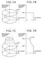
- FIG. 7A is a conceptual diagram showing a general cylindrical HSV color space whereas FIG. 7B is a model diagram showing a relation between a saturation (S) and a brightness/lightness value (V) in the cylindrical HSV color space;
- FIG. 7C is a conceptual diagram showing an enlarged cylindrical HSV color space in a fourth embodiment of the present invention whereas FIG. 7D is a model diagram showing a relation between the saturation (S) and the brightness/lightness value (V) in the enlarged cylindrical HSV color space;
- FIGS. 8A and 8B are each a model diagram showing a relation between the saturation (S) and the brightness/lightness value (V) in a cylindrical HSV color space enlarged by adding a white color to serve as a fourth color in a fourth embodiment of the present invention
- FIG. 9 is a diagram showing an existing HSV color space prior to addition of a white color to serve as a fourth color in the fourth embodiment, an HSV color space enlarged by adding a white color to serve as a fourth color in the fourth embodiment and a typical relation between the saturation (S) and brightness/lightness value (V) of a sub-pixel input signal;
- FIG. 10 is a diagram showing an existing HSV color space prior to addition of a white color to serve as a fourth color in the fourth embodiment, an HSV color space enlarged by adding a white color to serve as a fourth color in the fourth embodiment and a typical relation between the saturation (S) and brightness/lightness value (V) of a sub-pixel output signal completing an extension process;
- FIG. 11 is a model diagram showing sub-pixel input-signal values and sub-pixel output-signal values in an extension process of a method for driving an image display apparatus according to the fourth embodiment and a method for driving an image display apparatus assembly including the image display apparatus;
- FIG. 12 is a conceptual diagram showing an image display panel and a planar light-source apparatus which compose an image display apparatus assembly according to a fifth embodiment of the present invention.
- FIG. 13 is a diagram showing a planar light-source apparatus control circuit of the planar light-source apparatus employed in the image display apparatus assembly according to the fifth embodiment
- FIG. 14 is a model diagram showing locations and an array of elements such as planar light-source units in the planar light-source apparatus employed in the image display apparatus assembly according to the fifth embodiment;
- FIGS. 15A and 15B are each a conceptual diagram to be referred to in explanation of a state of increasing and decreasing a light-source luminance Y 2 of a planar light-source unit in accordance with control executed by a planar light-source apparatus driving circuit so that the planar light-source unit produces a second prescribed value Y 2 of the display luminance on the assumption that a control signal corresponding to a signal maximum value X max ⁇ (s, t) in the display area unit has been supplied to the sub-pixel;
- FIG. 16 is a diagram showing an equivalent circuit of an image display apparatus according to a sixth embodiment of the present invention.
- FIG. 17 is a conceptual diagram showing an image display panel employed in the image display apparatus according to the sixth embodiment.
- FIG. 18 is a model diagram showing locations of pixels and locations of pixel groups on an image display panel according to an eighth embodiment of the present invention.
- FIG. 19 is a model diagram showing other locations of pixels and other locations of pixel groups on the image display panel according to the eighth embodiment.
- FIG. 20 is a conceptual diagram of a planar light-source apparatus of an edge-light type (or a side-light type).
- the signal processing section receives the following sub-pixel input signals:
- a first sub-pixel input signal provided with a first sub-pixel input-signal value x 1 ⁇ (p1, q) ;
- a third sub-pixel input signal provided with a third sub-pixel input-signal value X 3 ⁇ (p1, q) .
- the signal processing section receives the following sub-pixel input signals:
- a first sub-pixel input signal provided with a first sub-pixel input-signal value x 1 ⁇ (p2, q) ;
- a third sub-pixel input signal provided with a third sub-pixel input-signal value X 3 ⁇ (p2, q) .
- the signal processing section With regard to the first pixel pertaining to the (p, q)th pixel group, the signal processing section generates the following sub-pixel output signals:
- a first sub-pixel output signal provided with a first sub-pixel output-signal value X 1 ⁇ (p1, q) and used for determining the display gradation of a first sub-pixel of the first pixel;
- a second sub-pixel output signal provided with a second sub-pixel output-signal value X 2 ⁇ (p1, q) and used for determining the display gradation of a second sub-pixel of the first pixel;
- a third sub-pixel output signal provided with a third sub-pixel output-signal value X 3 ⁇ (p1, q) and used for determining the display gradation of a third sub-pixel of the first pixel.
- the signal processing section With regard to the second pixel pertaining to the (p, q)th pixel group, the signal processing section generates the following sub-pixel output signals:
- a first sub-pixel output signal provided with a first sub-pixel output-signal value X 1 ⁇ (p2, q) and used for determining the display gradation of a first sub-pixel of the second pixel;
- a second sub-pixel output signal provided with a second sub-pixel output-signal value X 2 ⁇ (p2, q) and used for determining the display gradation of a second sub-pixel of the second pixel;
- a third sub-pixel output signal provided with a third sub-pixel output-signal value X 3 ⁇ (p2, q) and used for determining the display gradation of a third sub-pixel of the second pixel.
- the signal processing section With regard to a fourth sub-pixel pertaining to the (p, q)th pixel group, the signal processing section generates a fourth sub-pixel output signal provided with a fourth sub-pixel output-signal value X 4 ⁇ (p, q) and used for determining the display gradation of the fourth sub-pixel.
- notation p is a positive integer satisfying a relation 1 ⁇ p ⁇ P
- notation q is a positive integer satisfying a relation 1 ⁇ q ⁇ Q
- notation p 1 is a positive integer satisfying a relation 1 ⁇ p 1 ⁇ P
- notation q 1 is a positive integer satisfying a relation 1 ⁇ q 1 ⁇ Q
- notation P 2 is a positive integer satisfying a relation 1 ⁇ p 2 ⁇ P
- notation q 2 is a positive integer satisfying a relation 1 ⁇ q 2 ⁇ Q
- notation P is a positive integer representing the number of pixel groups laid out in the first direction
- notation Q is a positive integer representing the number of pixel groups laid out in the second direction.
- the signal processing section receives the same sub-pixel input signals and generates the same sub-pixel output signals as the signal processing section does in accordance with the method for driving the image display apparatus according to the first mode of the present invention or in accordance with the method for driving the image display apparatus assembly including the image display apparatus.
- the signal processing apparatus does not generate the third sub-pixel output signal for the third sub-pixel included in the second pixel pertaining to the (p, q)th pixel group.
- the signal processing section finds a fourth sub-pixel output signal on the basis of a first signal value found from a first sub-pixel input signal, a second sub-pixel input signal and a third sub-pixel input signal which are received for respectively the first, second and third sub-pixels pertaining to the first pixel included in every specific one of the pixel groups and on the basis of a second signal value found from a first sub-pixel input signal, a second sub-pixel input signal and a third sub-pixel input signal which are received for respectively the first, second and third sub-pixels pertaining to the second pixel included in the specific pixel group, outputting the fourth sub-pixel output signal to an image display panel driving circuit.
- the version is also referred to as the (1-A)th mode of the present invention for the sake of convenience.
- the version of the configuration according to the second mode is also referred to as the (2-A)th mode of the present invention for the sake of convenience.
- first sub-pixel output signals for respectively the first sub-pixels pertaining to respectively the first and second pixels included in the specific pixel group on the basis of the first sub-pixel mixed input signal and on the basis of the first sub-pixel input signals received for respectively the first sub-pixels pertaining to respectively the first and second pixels included in the specific pixel group;
- the fourth sub-pixel output signal outputs the fourth sub-pixel output signal, the first sub-pixel output signals for respectively the first sub-pixels pertaining to respectively the first and second pixels included in the specific pixel group, the second sub-pixel output signals for respectively the second sub-pixels pertaining to respectively the first and second pixels included in the specific pixel group and the third sub-pixel output signals for respectively the third sub-pixels pertaining to respectively the first and second pixels included in the specific pixel group.
- this other version is also referred to as the (1-B)th mode of the present invention for the sake of convenience.
- the method for driving the image display apparatus according to the second mode of the present invention can also be provided with another version similar to the other version described above.
- the signal processing section finds third sub-pixel output signals for respectively the third sub-pixels pertaining to respectively the first and second pixels included in the specific pixel group on the basis of the third sub-pixel mixed input signal and on the basis of the third sub-pixel input signals received for respectively the third sub-pixels pertaining to respectively the first and second pixels included in the specific pixel group.
- the signal processing section finds only a third sub-pixel output signal for the third sub-pixel pertaining to the first pixel included in the specific pixel group on the basis of the third sub-pixel mixed input signal.
- the other version of the method for driving the image display apparatus according to the second mode of the present invention is also referred to as the (2-B)th mode of the present invention for the sake of convenience.
- the signal processing section finds a third sub-pixel output signal on the basis of third sub-pixel input signals received for respectively the third sub-pixels pertaining to respectively the first and second pixels included in the specific pixel group, outputting the third sub-pixel output signal to an image display panel driving circuit.
- the second mode of the present invention includes this further version, the (2-A)th mode and the (2-B)th mode.
- (P ⁇ Q) pixel groups are laid out to form a 2-dimensional matrix in which P pixel groups are laid out in a first direction to form an array and Q such arrays are laid out in a second direction;
- each of the pixel groups includes a first pixel and a second pixel adjacent to the first pixel in the second direction;
- This configuration is also referred to as the (2a)th mode of the present invention for the sake of convenience.
- (P ⁇ Q) pixel groups are laid out to form a 2-dimensional matrix in which P pixel groups are laid out in a first direction to form an array and Q such arrays are laid out in a second direction;
- each of the pixel groups includes a first pixel and a second pixel adjacent to the first pixel in the second direction;
- This configuration is also referred to as the (2b)th mode of the present invention for the sake of convenience.
- operations to drive an image display apparatus adopting the method for driving the image display apparatus according to the second mode, which includes the further version explained earlier, the (2-A)th mode and the (2-B)th mode, and to drive an image display apparatus assembly employing the image display apparatus and a planar light-source apparatus for radiating illumination light to the rear face of the image display apparatus can be carried out on the basis of the method for driving the image display apparatus according to the second mode which includes the further version explained earlier, the (2-A)th mode and the (2-B)th mode.
- an image display apparatus based on the configuration according to the (2a)th mode and an image display apparatus assembly employing the image display apparatus based on the configuration according to the (2a)th mode and a planar light-source apparatus for radiating illumination light to the rear face of the image display apparatus.
- this configuration provided in accordance with the (1-A)th mode is also referred to as a (1-A-1)th mode whereas the configuration provided in accordance with the (2-A)th mode is also referred to as a (2-A-1)th mode.
- the first minimum value Min (p, q) ⁇ 1 is the smallest among the sub-pixel input-signal values x 1 ⁇ (p1, q) , x 2 ⁇ (p1, q) and x 3 ⁇ (p1, q)
- the second minimum value Min (p, q) ⁇ 2 is the smallest value among the sub-pixel input-signal values x 1 ⁇ (p2, q) , x 2 ⁇ (p2, q) and X 3 ⁇ (p2, q) .
- the first signal value SG (p, q) ⁇ 1 and the second signal value SG (p, q) ⁇ 2 can be expressed by equations given below. In the equations given below, each of notations c 11 and c 12 denotes a constant.
- the image display apparatus and/or the image display apparatus assembly employing the image display apparatus are prototyped and, typically, an image observer evaluates the image displayed by the image display apparatus and/or the image display apparatus assembly.
- the image observer properly determines a value to be used as the fourth sub-pixel output-signal value X 4 ⁇ (p, q) or an equation to be used to express the fourth sub-pixel output-signal value X 4 ⁇ (p, q) .
- Equations for expressing the first signal value SG (p, q) ⁇ 1 and the second signal value SG (p, q) ⁇ 2 are given as follows.
- SG (p,q) ⁇ 1 c 11 [Min (p,q) ⁇ 1 ]
- SG (p,q) ⁇ 2 c 11 [Min (p,q) ⁇ 2 ] or
- SG (p,q) ⁇ 1 c 12 [Min (p,q) ⁇ 1 ] 2
- SG (p,q) ⁇ 2 c 12 [Min (p,q) ⁇ 2 ] 2
- the first signal value SG (p, q) ⁇ 1 and the second signal value SG (p, q) ⁇ 2 are expressed by equations given below.
- each of notations c 13 , c 14 , c 15 and c 16 denotes a constant.
- SG (p,q) ⁇ 1 c 13 [Max (p,q) ⁇ 1 ] 1/2
- SG (p,q) ⁇ 2 c 13 [Max (p,q) ⁇ 2 ] 1/2 or
- SG (p,q) ⁇ 1 c 14 ⁇ [Min (p,q) ⁇ 1 /Max (p,q) ⁇ 1 ] or (2 n ⁇ 1) ⁇
- SG (p,q) ⁇ 2 c 14 ⁇ [Min (p,q) ⁇ 2 /Max (p,q) ⁇ 2 ] or (2 n ⁇ 1) ⁇
- the first signal value SG (p, q) ⁇ 1 and the second signal value SG (p, q) ⁇ 2 are expressed by equations given below.
- SG (p,q) ⁇ 1 c 15 ( ⁇ (2 n ⁇ 1) ⁇ Min (p,q) ⁇ 1 /[Max (p,q) ⁇ 1 ⁇ Min (p,q) ⁇ 1 ] ⁇ or (2 n ⁇ 1))
- SG (p,q) ⁇ 2 c 15 ( ⁇ (2 n ⁇ 1) ⁇ Min (p,q) ⁇ 2 /[Max (p,q) ⁇ 2 ⁇ Min (p,q) ⁇ 2 ⁇ or (2 n ⁇ 1))
- the first signal value SG (p, q) ⁇ 1 and the second signal value SG (p, q) ⁇ 2 are expressed by equations given below.
- SG (p,q) ⁇ 1 The smaller one of c 16 ⁇ [Max (p,q) ⁇ 1 ] 1/2 and c 16 ⁇ Min (p,q) ⁇ 1
- SG (p,q) ⁇ 2 The smaller one of c 16 ⁇ [Max (p,q) ⁇ 2 ] 1/2 and c 16 ⁇ Min (p,q) ⁇ 2
- the first signal value SG (p, q) ⁇ 1 is determined on the basis of a saturation S (p, q) ⁇ 1 in an HSV color space, a brightness/lightness value V (p, q) ⁇ 1 in the HSV color space and a constant ⁇ which is dependent on the image display apparatus.
- the second signal value SG (p, q) ⁇ 2 is determined on the basis of a saturation S (p, q) ⁇ 2 in the HSV color space, a brightness/lightness value V (p, q) ⁇ 2 in the HSV color space and the constant ⁇ .
- this configuration for the (1-A)th mode is also referred to as a (1-A-2)th mode whereas this configuration for the (2-A)th mode is also referred to as a (2-A-2)th mode.
- Max (p, q) ⁇ 1 denotes the largest value among the three sub-pixel input-signal values x 1 ⁇ (p1, q) , X 2 ⁇ (p1, q) and X 3 ⁇ (p1, q) ;
- Min (p, q) ⁇ 1 denotes the smallest value among the three sub-pixel input-signal values x 1 ⁇ (p1, q) , x 2 ⁇ (p1, q) and x 3 ⁇ (p1, q) ;
- Max (p, q) ⁇ 2 denotes the largest value among the three sub-pixel input-signal values x 1 ⁇ (p2, q) , x 2 ⁇ (p2, q) and x 3 ⁇ (p2, q) ;
- Min (p, q) ⁇ 2 denotes the smallest value among the three sub-pixel input-signal values x 1 ⁇ (p2, q) , x 2 ⁇ (p2, q) and x 3 ⁇ (p2, q) .
- the saturation S can have a value in the range 0 to 1 whereas the brightness/lightness value V is a value in the range 0 to (2 n ⁇ 1) where notation n is a positive integer representing the number of gradation bits.
- notation H denotes a color phase (or a hue) which indicates the type of the color
- notation S denotes a saturation (or a chromaticity) which indicates the vividness of the color
- notation V denotes a brightness/lightness value which indicates the brightness of the color.
- a first sub-pixel output-signal value X 1 ⁇ (p1, q) is found on the basis of at least the first sub-pixel input-signal value x 1 ⁇ (p1, q) , the first maximum value Max (p, q) ⁇ 1 , the first minimum value Min (p, q) ⁇ 1 and the first signal value SG (p, q) ⁇ 1 .
- a second sub-pixel output-signal value X 2 ⁇ (p1, q) is found on the basis of at least the second sub-pixel input-signal value X 2 ⁇ (p1, q) , the first maximum value Max (p, q) ⁇ 1 , the first minimum value Min (p, q) ⁇ 1 and the first signal value SG (p, q) ⁇ 1 .
- a third sub-pixel output-signal value X 3 ⁇ (p1, q) is found on the basis of at least the third sub-pixel input-signal value x 3 ⁇ (p1, q) , the first maximum value Max (p, q) ⁇ 1 , the first minimum value Min (p, q) ⁇ 1 and the first signal value SG (p, q) ⁇ 1 .
- a first sub-pixel output-signal value X 1 ⁇ (p2, q) is found on the basis of at least the first sub-pixel input-signal value x 1 ⁇ (p2, q) , the second maximum value Max (p, q) ⁇ 2, the second minimum value Min (p, q) ⁇ 2 and the second signal value SG (p, q) ⁇ 2 .
- a second sub-pixel output-signal value X 2 ⁇ (p2, q) is found on the basis of at least the second sub-pixel input-signal value x 2 ⁇ (p2, q) , the second maximum value Max (p, q) ⁇ 2 , the second minimum value Min (p, q) ⁇ 2 and the second signal value SG (p, q) ⁇ 2 .
- a third sub-pixel output-signal value X 3 ⁇ (p2, q) is found on the basis of at least the third sub-pixel input-signal value x 3 ⁇ (p2, q) , the second maximum value Max (p, q) ⁇ 2 , the second minimum value Min (p, q) ⁇ 2 and the second signal value SG (p, q) ⁇ 2 .
- a first sub-pixel output-signal value X 1 ⁇ (p1, q) is found on the basis of at least the first sub-pixel input-signal value x 1 ⁇ (p1, q) , the first maximum value Max (p, q) ⁇ 1 , the first minimum value Min (p, q) ⁇ 1 and the first signal value SG (p, q) ⁇ 1 .
- a second sub-pixel output-signal value X 2 ⁇ (p1, q) is found on the basis of at least the second sub-pixel input-signal value x 2 ⁇ (p1, q) , the first maximum value Max (p, q) ⁇ 1 , the first minimum value Min (p, q) ⁇ 1 and the first signal value SG (p, q) ⁇ 1 .
- a first sub-pixel output-signal value X 1 ⁇ (p2, q) is found on the basis of at least the first sub-pixel input-signal value x 1 ⁇ (p2, q) , the second maximum value Max (p, q) ⁇ 2 , the second minimum value Min (p, q) ⁇ 2 and the second signal value SG (p, q) ⁇ 2 .
- a second sub-pixel output-signal value X 2 ⁇ (p2, q) is found on the basis of at least the second sub-pixel input-signal value x 2 ⁇ (p2, q), the second maximum value Max (p, q) ⁇ 2 , the second minimum value Min (p, q) ⁇ 2 and the second signal value SG (p, q) ⁇ 2 .
- each of the above configurations is also referred to as a first configuration for the sake of convenience.
- notation Max (p, q) ⁇ 1 denotes the largest value among the sub-pixel input-signal values x 1 ⁇ (p1, q) , x 2 ⁇ (p1, q) and x 3 ⁇ (p1, q)
- notation Max (p, q) ⁇ 2 denotes the largest value among the sub-pixel input-signal values x 1 ⁇ (p2, q) , x 2 ⁇ (p2, q) and x 3 ⁇ (p2, q) .
- the first sub-pixel output-signal value X 1 ⁇ (p1, q) is found on the basis of at least the first sub-pixel input-signal value x 1 ⁇ (p1, q) , the first maximum value Max (p, q) ⁇ 1 , the first minimum value Min (p, q) ⁇ 1 and the first signal value SG (p, q) ⁇ 1 .
- the first sub-pixel output-signal value X 1 ⁇ (p1, q) can also be found on the basis of [x 1 ⁇ (p1, q) , Max (p q) ⁇ 1 , Min (p, q) ⁇ 1 , SG (p, q) ⁇ 1 ] or on the basis of [x 1 ⁇ (p1, q) , x 1 ⁇ (p2, q) , Max (p, q) ⁇ 1 , Min (p, q) ⁇ 1 , SG (p, q) ⁇ 1 ].
- the second sub-pixel output-signal value X 2 ⁇ (p1, q) is found on the basis of at least the second sub-pixel input-signal value x 2 ⁇ (p1, q) the first maximum value Max (p, q) ⁇ 1 , the first minimum value Min (p, q) ⁇ 1 and the first signal value SG (p, q) ⁇ 1 .
- the second sub-pixel output-signal value X 2 ⁇ (p1, q) can also be found on the basis of [x 2 ⁇ (p1, q) , Max (p, q) ⁇ 1 , Min (p, q) ⁇ 1 , SG (p, q) ⁇ 1 ] or on the basis of [x 2 ⁇ (p1, q) , x 2 ⁇ (p2,q) , Max (p, q) ⁇ 1 , Min (p, q) ⁇ 1 , SG (p, q) ⁇ 1 ].
- the third sub-pixel output-signal value X 3 ⁇ (p1, q) is found on the basis of at least the third sub-pixel input-signal value x 3 ⁇ (p1, q) , the first maximum value Max (p, q) ⁇ 1 , the first minimum value Min (p, q) ⁇ 1 and the first signal value SG (p, q) ⁇ 1 .
- the third sub-pixel output-signal value X 3 ⁇ (p1, q) can also be found on the basis of [x 3 ⁇ (p1, q) , Max (p, q) ⁇ 1 , Min (p, q) ⁇ 1 , SG (p, q) ⁇ 1 ] or on the basis of [x 3 ⁇ (p1, q) , x 3 ⁇ (p2, q) , Max (p q) ⁇ 1 , Min (p, q) ⁇ 1 , SG (p, q) ⁇ 1 ].
- the first sub-pixel output-signal value X 1 ⁇ (p2, q) , the second sub-pixel output-signal value X 2 ⁇ (p2, q) and the third sub-pixel output-signal value X 3 ⁇ (p2, q) can be found in the same way as the first sub-pixel output-signal value X 1 ⁇ (p1, q) , the second sub-pixel output-signal value X 2 ⁇ (p1, q) and the third sub-pixel output-signal value X 3 ⁇ (p1, q) respectively.
- each of notations C 1 and C 2 denotes a constant and the fourth sub-pixel output-signal value X 4 ⁇ (p, q) satisfies a relation X 4 ⁇ (p, q) ⁇ (2 n ⁇ 1).
- the fourth sub-pixel output-signal value X 4 ⁇ (p, q) is set at (2 n ⁇ 1).
- one of Eqs. (1-A), (1-B) and (1-C) can be selected in accordance with the value of the first signal value SG (p, q) ⁇ 1 , in accordance with the value of the second signal value SG (p, q) ⁇ 2 or in accordance with the values of both the first signal value SG (p, q) ⁇ 1 and the second signal value SG (p, q) ⁇ 2 . That is to say, in every pixel group, one of Eqs. (1-A), (1-B) and (1-C) can be determined to serve as a common equation shared by all pixel groups for finding the fourth sub-pixel output-signal value X 4 ⁇ (p, q) or one of Eqs. (1-A), (1-B) and (1-C) can be selected for every pixel group.
- a maximum brightness/lightness value V max (S) expressed as a function of variable saturation S to serve as the maximum of a brightness/lightness value V in an HSV color space enlarged by adding the fourth color is stored in the signal processing section.
- the signal processing section carries out the following processes of:
- each of the configuration described for the (1-A-2)th mode and the configuration described for the (2-A-2)th mode is also referred to as a second configuration for the sake of convenience.
- the first signal value SG (p, q) ⁇ 1 is determined on the basis of the first minimum value Min (p, q) ⁇ 1 and the extension coefficient ⁇ 0 whereas the second signal value SG (p, q) ⁇ 2 is determined on the basis of the second minimum value Min (p, q) ⁇ 2 and the extension coefficient ⁇ 0 .
- the first signal value SG (p, q) ⁇ 1 and the second signal value SG (p, q) ⁇ 2 can be expressed by equations given below. In the equations given below, each of notations c 21 and c 22 denotes a constant.
- the image display apparatus and/or the image display apparatus assembly employing the image display apparatus are prototyped and, typically, an image observer evaluates the image displayed by the image display apparatus and/or the image display apparatus assembly.
- the image observer properly determines a value to be used as the fourth sub-pixel output-signal value X 4 ⁇ (p, q) or an equation to be used to express the fourth sub-pixel output-signal value X 4 ⁇ (p, q) .
- the first signal value SG (p, q) ⁇ 1 and the second signal value SG (p, q) ⁇ 2 are expressed by other equations given below.
- each of notations c 23 , c 24 , c 25 and c 26 denotes a constant.
- the first signal value SG (p, q) ⁇ 1 and the second signal value SG (p, q) ⁇ 2 are expressed by equations given as follows.
- SG (p,q) ⁇ 1 c 25 ( ⁇ 0 ⁇ (2 n ⁇ 1) ⁇ Min (p,q) ⁇ 1 /[Max (p,q) ⁇ 1 ⁇ Min (p,q) ⁇ 1 ] ⁇ or ⁇ 0 ⁇ (2 n ⁇ 1))
- SG (p,q) ⁇ 2 c 25 ( ⁇ 0 ⁇ (2 n ⁇ 1) ⁇ Min (p,q) ⁇ 2 /[Max (p,q) ⁇ 2 ⁇ Min (p,q) ⁇ 2 ] ⁇ or ⁇ 0 ⁇ (2 n ⁇ 1))
- the first signal value SG (p, q) ⁇ 1 and the second signal value SG (p, q) ⁇ 2 are expressed by equations given as follows.
- SG (p,q) ⁇ 1 The product of ⁇ 0 and the smaller one of c 26 ⁇ [Max (p,q) ⁇ 1 ] 1/2 and c 26 ⁇ Min (p,q) ⁇ 1
- SG (p,q) ⁇ 2 The product of ⁇ 0 and the smaller one of c 26 ⁇ [Max (p,q) ⁇ 2 ] 1/2 and c 26 ⁇ Min (p,q) ⁇ 2
- the second sub-pixel output-signal value X 2 ⁇ (p1, q) is found on the basis of at least the second sub-pixel input-signal value x 2 ⁇ (p1, q) , the extension coefficient ⁇ 0 and the first signal value SG (p, q) ⁇ 1 .
- the second sub-pixel output-signal value X 2 ⁇ (p1, q) can also be found on the basis of [x 2 ⁇ (p1, q) , ⁇ 0 , SG (p, q) ⁇ 1 ] or on the basis of [x 2 ⁇ (p1, q) , x 2 ⁇ (p2, q) , ⁇ 0 , SG (p, q) ⁇ 1 ].
- the third sub-pixel output-signal value X 3 ⁇ (p1, q) is found on the basis of at least the third sub-pixel input-signal value x 3 ⁇ (p1, q) , the extension coefficient ⁇ 0 and the first signal value SG (p, q) ⁇ 1 .
- the third sub-pixel output-signal value X 3 ⁇ (p1, q) can also be found on the basis of [x 3 ⁇ (p1, q) , ⁇ 0 , SG (p, q) ⁇ 1 ] or on the basis of [x 3 ⁇ (p1, q) , x 3 ⁇ (p2, q) , ⁇ 0 , SG (p, q) ⁇ 1 ].
- the first sub-pixel output-signal value X 1 ⁇ (p2, q) , the second sub-pixel output-signal value X 2 ⁇ (p2, q) and the third sub-pixel output-signal value X 3 ⁇ (p2, q) can be found in the same way as the first sub-pixel output-signal value X 1 ⁇ (p1, q) , the second sub-pixel output-signal value X 2 ⁇ (p1, q) and the third sub-pixel output-signal value X 3 ⁇ (p1, q) respectively.
- each of notations C 1 and C 2 denotes a constant and the fourth sub-pixel output-signal value X 4 ⁇ (p, q) satisfies a relation X 4 ⁇ (p, q) ⁇ (2 n ⁇ 1).
- the fourth sub-pixel output-signal value X 4 ⁇ (p, q) is set at (2 n ⁇ 1).
- one of Eqs. (2-A), (2-B) and (2-C) can be selected in accordance with the value of the first signal value SG (p, q) ⁇ 1 , in accordance with the value of the second signal value SG (p, q) ⁇ 2 or in accordance with the values of both the first signal value SG (p, q) ⁇ 1 and the second signal value SG (p, q) ⁇ 2 . That is to say, in every pixel group, one of Eqs. (2-A), (2-B) and (2-C) can be determined to serve as a common equation used in all pixel groups for finding the fourth sub-pixel output-signal value X 4 ⁇ (p, q) or one of Eqs. (2-A), (2-B) and (2-C) can be selected for every pixel group.
- the number of pixels composing every pixel group can be set at 3 or an integer greater than 3 (that is, p 0 ⁇ 3).
- the row direction of the 2-dimensional matrix cited before is taken as the first direction whereas the column direction of the matrix is taken as the second direction.
- Q denote a positive integer representing the number of pixel groups arranged in the second direction.
- the first pixel on the q′th column of the 2-dimensional matrix is placed at a location adjacent to the location of the first pixel on the (q′+1)th column of the matrix whereas the fourth sub-pixel on the q′th column is placed at a location not adjacent to the location of the fourth sub-pixel on the (q′+1)th column where notation q′ denotes an integer satisfying the relations 1 ⁇ q′ ⁇ (Q ⁇ 1)
- the image display apparatus assembly provided by the embodiments of the present invention as an assembly including desirable implementations and desirable configurations as described above, it is desirable to provide a scheme in which the luminance of illumination light radiated by the planar light-source apparatus to the rear face of the image display apparatus employed in the image display apparatus assembly is reduced on the basis of the extension coefficient ⁇ 0 .
- a maximum brightness/lightness value V max (S) expressed as a function of variable saturation S to serve as the maximum of a brightness/lightness value V in an HSV color space enlarged by adding the fourth color is stored in the signal processing section.
- the signal processing section carries out the following processes of:
- the present invention increases not only the luminance of light emitted by the white-color display sub-pixel, but also the luminance of light emitted by each of the red-color display sub-pixel, the green-color display sub-pixel and the blue-color display sub-pixel.
- the present invention is capable of avoiding the problem of the generation of the color dullness with a high degree of reliability.
- the luminance of a displayed image can be increased with the implementation and configuration.
- the present invention is optimum for displaying an image such as a static image, an advertisement image or an image displayed in a wait state in a cellular phone.
- the luminance of illumination light generated by the planar light-source apparatus can be reduced on the basis of the extension coefficient ⁇ 0 .
- the power consumption of the planar light-source apparatus can be decreased as well.
- the signal processing section is capable of finding the sub-pixel output-signal values X 1 ⁇ (p1, q) , X 2 ⁇ (p1, q) , X 3 ⁇ (p1, q) , X 1 ⁇ (p2, q) , X 2 ⁇ (p2, q) and X 3 ⁇ (p2, q) on the basis of the extension coefficient ⁇ 0 and the constant ⁇ .
- the signal processing section is capable of finding the sub-pixel output-signal values X 1 ⁇ (p1, q) , X 2 ⁇ (p1, q) , X 3 ⁇ (p1, q) , X 1 ⁇ (p2, q) , X 2 ⁇ (p2, q) and X 3 ⁇ (p2, q) in accordance with the following equations.
- reference notation BN 1-3 denotes the luminance of light emitted by a pixel serving as a set of first, second and third sub-pixels for a case in which it is assumed that a signal having a value corresponding to the maximum signal value of a first sub-pixel output signal is received for the first sub-pixel, a signal having a value corresponding to the maximum signal value of a second sub-pixel output signal is received for the second sub-pixel and a signal having a value corresponding to the maximum signal value of a third sub-pixel output signal is received for the third sub-pixel.
- reference notation BN 4 denotes the luminance of light emitted by a fourth sub-pixel for a case in which it is assumed that a signal having a value corresponding to the maximum signal value of a fourth sub-pixel output signal is received for the fourth sub-pixel.
- the constant ⁇ has a value peculiar to the image display panel, the image display apparatus and the image display apparatus assembly and is, thus, determined uniquely in accordance with the image display panel, the image display apparatus and the image display apparatus assembly.
- extension coefficient ⁇ 0 is set at a value ⁇ min smallest among values found for a plurality of pixels as the values of V max (S)/V(S)[ ⁇ (S)].
- ⁇ min is taken as the extension coefficient ⁇ 0 .
- the extension coefficient ⁇ 0 is found on the basis of at least one value of V max (S)/V(S)[ ⁇ (S)] found for a plurality of pixels.
- the extension coefficient ⁇ 0 can also be found on the basis of one value such as the smallest value ⁇ min or, as a further alternative, a plurality of relatively small values of ⁇ (S) are sequentially found, starting with the smallest value ⁇ min , and an average ⁇ ave of the relatively small values of ⁇ (S) starting with the smallest value ⁇ min is taken as the extension coefficient ⁇ 0 .
- the fourth color is by no means limited to the white color. That is to say, the fourth color can be a color other than the white color.
- the fourth color can also be the yellow, cyan or magenta color.
- an image display apparatus is a color liquid-crystal display apparatus
- a configuration which further includes a first color filter placed between the first sub-pixel and the image observer to serve as a filter for passing light of the first elementary color, a second color filter placed between the second sub-pixel and the image observer to serve as a filter for passing light of the second elementary color and a third color filter placed between the third sub-pixel and the image observer to serve as a filter for passing light of the third elementary color.
- At least one of the ratios P 0 /P′ and Q/Q′ must be positive integers each equal to or greater than 2. It is to be noted that concrete examples of the ratios P 0 /P′ and Q/Q′ are 2, 4, 8, 16 and so on which are each an nth power of 2 where notation n is a positive integer.
- a light emitting device can be used as each light source composing the planar light-source apparatus.
- an LED Light Emitting Diode
- the light emitting diode serving as a light emitting device occupies only a small space so that a plurality of light emitting devices can be arranged with ease.
- a typical example of the light emitting diode serving as a light emitting device is a white-light emitting diode.
- the white-light emitting diode is a light emitting diode which radiates illumination light of the white color.
- the white-light emitting diode is obtained by combining an ultraviolet-light emitting diode or a blue-light emitting diode with a light emitting particle.
- Typical examples of the light emitting particle are a red-light emitting fluorescent particle, a green-light emitting fluorescent particle and a blue-light emitting fluorescent particle.
- Typical materials for making the red-light emitting fluorescent particle are Y 2 O 3 : Eu, YVO 4 :Eu, Y (P, V) O 4 :Eu, 3.5 MgO.0.5 MgF 2 .Ge 2 :Mn, CaSiO 3 :Pb, Mn, Mg 6 AsO 11 :Mn, (Sr, Mg) 3 (PO 4 ) 3 :Sn, La 2 O 2 S:Eu, Y 2 O 2 S:Eu, (ME:Eu) S, (M:Sm) x (Si, Al) 12 (O, N) 16 , ME 2 Si 5 N 8 :Eu, (Ca:Eu) SiN 2 and (Ca:Eu) AlSiN 3 .
- Symbol ME in (ME:Eu) S means an atom of at least one type selected from groups of Ca, Sr and Ba.
- Symbol ME used in the material names following (ME:Eu) S means the same as that in (ME:Eu) S.
- symbol M in (M:Sm) x (Si, Al) 12 (O, N) 16 means an atom of at least one type selected from groups of Li, Mg and Ca.
- Symbol M in the material names following (M:Sm) x (Si, Al) 12 (O, N) 16 means the same as that in (M:Sm) x (Si, Al) 12 (O, N) 16 .
- typical materials for making the green-light emitting fluorescent particle are LaPO 4 :Ce, Tb, BaMgAl 10 O 17 :Eu, Mn, Zn 2 SiO 4 :Mn, MgAl 11 O 19 :Ce, Tb, Y 2 SiO 5 :Ce, Tb, MgAl 11 O 19 :CE, Tb and Mn.
- Typical materials for making the green-light emitting fluorescent particle also include (Me:Eu) Ga 2 S 4 , (M:RE) x (Si, Al) 12 (O, N) 16 , (M:Tb) x (Si, Al) 12 (O, N) 16 and (M:Yb) x (Si, Al) 12 (O, N) 16 .
- RE in (M:RE) x (Si, Al) 12 (O, N) 16 means Tb and Yb.
- typical materials for making the blue-light emitting fluorescent particle are BaMgAl 10 O 17 :Eu, BaMg 2 Al 16 O 27 :Eu, Sr 2 P 2 O 7 :Eu, Sr 5 (PO 4 ) 3 Cl:Eu, (Sr, Ca, Ba, Mg) 5 (PO 4 ) 3 Cl:Eu, CaWO 4 , and CaWO 4 :Pb.
- the light emitting particle is by no means limited to the fluorescent particle.
- the light emitting particle can be a light emitting particle having a quantum well structure such as a 2-dimensional quantum well structure, a 1-dimensional quantum well structure (or a quantum fine line) or a 0-dimensional quantum well structure (or a quantum dot).
- the light emitting particle having a quantum well structure typically makes use of a quantum effect by localizing a wave function of carriers in order to convert the carriers into light with a high degree of efficiency in a silicon-family material of an indirect transition type in the same way as a direct transition type.
- the light emitting particle can be a light emitting particle applying this technology.
- the light source of the planar light-source apparatus can be configured as a combination of a red-light emitting device for emitting light of the red color, a green-light emitting device for emitting light of the green color and a blue-light emitting element for emitting light of the blue color.
- a typical example of the light of the red color is light having a main light emission waveform of 640 nm
- a typical example of the light of the green color is light having a main light emission waveform of 530 nm
- a typical example of the light of the blue color is light having a main light emission waveform of 450 nm.
- a typical example of the red-light emitting device is a light emitting diode
- a typical example of the green-light emitting device is a light emitting diode of the GaN family
- a typical example of the blue-light emitting device is a light emitting diode of the GaN family.
- the light source may also include light emitting devices for emitting light of the fourth color, the fifth color and so on which are other than the red, green and blue colors.
- the LED may have the so-called face-up structure or a flip-chip structure. That is to say, the light emitting diode is configured to have a substrate and a light emitting layer created on the substrate.
- the substrate and the light emitting layer may form a structure in which light is radiated from the light emitting layer to the external world.
- the substrate and the light emitting layer may form a substrate in which light is radiated from the light emitting layer to the external world by way of the substrate.
- the light emitting diode has a laminated structure typically including a substrate, a first chemical compound semiconductor layer created on the substrate to serve as a layer of a first conduction type such as the n-conduction type, an active layer created on the first chemical compound semiconductor layer and a second chemical compound semiconductor layer created on the active layer to serve as a layer of a second conduction type such as the p-conduction type.
- the light emitting diode has a first electrode electrically connected to the first chemical compound semiconductor layer and a second electrode electrically connected to the second chemical compound semiconductor layer.
- Each of the layers composing the light emitting diode can be made from a generally known chemical compound semiconductor material which is selected on the basis of the wavelength of light to be emitted by the light emitting diode.
- the planar light-source apparatus also referred to as a backlight can have one of two types. That is to say, the planar light-source apparatus can be a planar light-source apparatus of a right-below type disclosed in documents such as Japanese Patent Laid-Open No. Sho 63-187120 and Japanese Patent Laid-open No. 2002-277870 or a planar light-source apparatus of an edge-light type (or a side-light type) disclosed in documents such as Japanese Patent Laid-open No. 2002-131552.
- the light emitting devices each described previously to serve as a light source can be laid out to form an array in a case.
- the arrangement of the light emitting devices is by no means limited to such a configuration.
- the array of these light emitting devices is composed of a plurality of sets each including a red-color light emitting device, a green-color light emitting device and a blue-color light emitting device.
- the set is a group of light emitting devices employed in an image display panel.
- the groups each including light emitting devices compose an image display apparatus.
- a plurality of light emitting device groups are laid out continuously in the horizontal direction of the display screen of the image display panel to form a continuous array of groups each including light emitting devices.
- a plurality of such arrays of groups each including light emitting devices are laid out in the vertical direction of the display screen of the image display panel to form a 2-dimensional matrix.
- a light emitting device group is composed of one red-color light emitting device, one green-color light emitting device and one blue-color light emitting device.
- a light emitting device group may be composed of one red-color light emitting device, two green-color light emitting devices and one blue-color light emitting device.
- a light emitting device group may be composed of two red-color light emitting devices, two green-color light emitting devices and one blue-color light emitting device. That is to say, a light emitting device group is one of a plurality of combinations each composed of red-color light emitting devices, green-color light emitting devices and blue-color light emitting devices.
- the light emitting device can be provided with a light fetching lens like one described on page 128 of Nikkei Electronics, No. 889, Dec. 20, 2004.
- each of the planar light-source units can be implemented as one aforementioned group of light emitting devices or at least two such groups each including light emitting devices.
- each planar light-source unit can be implemented as one white-color light emitting diode or at least two white-color light emitting diodes.
- a separation wall can be provided between every two adjacent planar light-source units.
- the separation wall can be made from a nontransparent material which does not pass on light radiated by a light emitting device of the planar light-source apparatus.
- a material are the acryl family resin, the polycarbonate resin and the ABS resin.
- the separation wall can also be made from a material which passes on light radiated by a light emitting device of the planar light-source apparatus.
- such a material are the polymethacrylic methyl acid resin (PMMA), the polycarbonate resin (PC), the polyarylate resin (PAR), the polyethylene terephthalate resin (PET) and glass.
- a light diffusion/reflection function or a mirror-surface reflection function can be provided on the surface of the partition wall.
- unevenness is created on the surface of the partition wall by adoption of a sand blast technique or by pasting a film having unevenness on the surface thereof to the surface of the separation wall to serve as a light diffusion film.
- a light reflection film is pasted to the surface of the partition wall or a light reflection layer is created on the surface of the partition wall by carrying out a coating process for example.
- the planar light-source apparatus of the right-below type can be configured to have a light diffusion plate, an optical function sheet group and a light reflection sheet.
- the optical function sheet group typically includes a light diffusion sheet, a prism sheet and a light polarization conversion sheet.
- a commonly known material can be used for making each of the light diffusion plate, the light diffusion sheet, the prism sheet, the light polarization conversion sheet and the light reflection sheet.
- the optical function sheet group may include a plurality of sheets which are separated from each other by a gap or stacked on each other to form a laminated structure.
- the light diffusion sheet, the prism sheet and the light polarization conversion sheet can be stacked on each other to form a laminated structure.
- the light diffusion plate and the optical function sheet group are provided between the planar light-source apparatus and the image display panel.
- a light guiding plate is provided to face the image display panel.
- a concrete example of the image display panel is the image display panel employed in a liquid-crystal display apparatus.
- light emitting devices are provided on a side face of the light guiding plate.
- the side face of the light guiding plate is referred to as a first side face.
- the light guiding plate has a bottom face serving as a first face, a top face serving as a second face, the first side face cited above, a second side face, a third side face facing the first side face and a fourth side face facing the second side face.
- a typical example of a more concrete whole shape of the light guiding plate is a top-cut square conic shape resembling a wedge.
- the two mutually facing side faces of the top-cut square conic shape correspond to the first and second faces respectively whereas the bottom face of the top-cut square conic shape corresponds to the first side face.
- the second face of the light guiding plate can be made smooth like a mirror surface or provided with blast engraving surface having a light diffusion effect so as to create a surface with infinitesimal unevenness portions.
- the bottom face (or the first face) of the light guiding plate is desirable to provide the bottom face (or the first face) of the light guiding plate with protrusions and/or dents. That is to say, it is desirable to provide the first face of the light guiding plate with protrusions, dents or unevenness portions including protrusions and dents. If the first face of the light guiding plate is provided with unevenness portions including protrusions and dents, a protrusion and a dent can be placed at contiguous locations or noncontiguous locations. It is possible to provide a configuration in which the protrusions and/or the dents provided on the first face of the light guiding plate are aligned in a stretching direction which forms an angle determined in advance in conjunction with the direction of illumination light incident to the light guiding plate.
- the cross-sectional shape of contiguous protrusions or contiguous dents for a case in which the light guiding plate is cut over a virtual plane vertical to the first face in the direction of illumination light incident to the light guiding plate is typically the shape of a triangle, the shape of any quadrangle such as a square, a rectangle or a trapezoid, the shape of any polygon or a shape enclosed by a smooth curve.
- Examples of the shape enclosed by a smooth curve are a circle, an eclipse, a paraboloid, a hyperboloid and a catenary.
- the predetermined angle formed by the direction of illumination light incident to the light guiding plate in conjunction with the stretching direction of the protrusions and/or the dents provided on the first face of the light guiding plate has a value in the range 60 to 120 degrees. That is to say, if the direction of illumination light incident to the light guiding plate corresponds to the angle of 0 degrees, the stretching direction corresponds to an angle in the range 60 to 120 degrees.
- every protrusion and/or every dent which are provided on the first face of the light guiding plate can be configured to serve respectively as every protrusion and/or every dent which are laid out non-contiguously in a stretching direction forming an angle determined in advance in conjunction with the direction of illumination light incident to the light guiding plate.
- the shape of noncontiguous protrusions and noncontiguous dents can be the shape of a pyramid, the shape of a circular cone, the shape of a cylinder, the shape of a polygonal column such as a triangular column or a rectangular column or any of a variety of cubical shapes enclosed by a smooth curved surface.
- Typical examples of a cubical shape enclosed by a smooth curved surface are a portion of a sphere, a portion of a spheroid, a portion of a cubic paraboloid and a portion of a cubic hyperboloid.
- the light guiding plate may include protrusions and dents. These protrusions and dents are formed on the peripheral edges of the first face of the light guiding plate.
- illumination light radiated by a light source to the light guiding plate collides with either of a protrusion and a dent which are created on the first face of the light guiding plate and is dispersed.
- the height, depth, pitch and shape of every protrusion and/or every dent can be fixed or changed in accordance with the distance from the light source. If the height, depth, pitch and shape of every protrusion and/or every dent are changed in accordance with the distance from the light source, for example, the pitch of every protrusion and the pitch of every dent can be made smaller as the distance from the light source increases.
- the pitch of every protrusion or the pitch of every dent means a pitch extended in the direction of illumination light incident to the light guiding plate.
- a planar light-source apparatus provided with a light guiding plate
- a light reflection member facing the first face of the light guiding plate.
- an image display panel is placed to face the second face of the light guiding plate.
- the liquid-crystal display apparatus is placed to face the second face of the light guiding plate.
- Light emitted by a light source reaches the light guiding plate from the first side face which is typically the bottom face of the top-cut square conic shape. Then, the light collides with a protrusion or a dent and is dispersed. Subsequently, the light is radiated from the first face and reflected by the light reflection member to again arrive at the first face.
- the light is radiated from the second face to the image display panel.
- a light diffusion sheet or a prism sheet can be placed at a location between the second face of the light guiding plate and the image display panel.
- the illumination light radiated by the light source can be led directly or indirectly to the light guiding plate. If the illumination light radiated by the light source is led indirectly to the light guiding plate, an optical fiber is typically used for leading the light to the light guiding plate.
- the material for making the light guiding plate includes glass and plastic materials such as the polymethacrylic methyl acid resin (PMMA), the polycarbonate resin (PC), the acryl family resin, the amorphous polypropylene family resin and the styrene family resin including the AS resin.
- PMMA polymethacrylic methyl acid resin
- PC polycarbonate resin
- acryl family resin the acryl family resin
- amorphous polypropylene family resin the amorphous polypropylene family resin
- styrene family resin including the AS resin.
- the method for driving the planar light-source apparatus and the condition for driving the apparatus are not prescribed in particular.
- the light sources can be controlled collectively. That is to say, for example, a plurality of light emitting devices are driven at the same time.
- the light emitting devices are driven in units each including a plurality of light emitting devices.
- This driving method is referred to as a group driving technique.
- the planar light-source apparatus is composed of a plurality of planar light-source units whereas the display area of the image display panel is divided into the same plurality of virtual display area units.
- the planar light-source apparatus is composed of (S ⁇ T) planar light-source units whereas the display area of the image display panel is divided into (S ⁇ T) virtual display area units each associated with one of the (S ⁇ T) planar light-source units.
- the light emission state of each of the (S ⁇ T) planar light-source units is driven individually.
- a driving circuit for driving the planar light-source apparatus is referred to as a planar light-source apparatus driving circuit which typically includes an LED (Light Emitting Device) driving circuit, a processing circuit and a storage device (to serve as a memory).
- a driving circuit for driving the image display panel is referred to as an image display panel driving circuit which is composed of commonly known circuits. It is to be noted that a temperature control circuit may be employed in the planar light-source apparatus driving circuit.
- the control of the display luminance and the light-source luminance is executed for each image display frame.
- the display luminance is the luminance of illumination light radiated from a display area unit whereas the light-source luminance is the luminance of illumination light emitted by a planar light-source unit.
- the driving circuits described above receive a frame frequency also referred to as a frame rate and a frame time which is expressed in terms of seconds.
- the frame frequency is the number of images transmitted per second whereas the frame time is the reciprocal of the frame frequency.
- a transmission-type liquid-crystal display apparatus typically includes a front panel, a rear panel and a liquid-crystal material sandwiched by the front and rear panels.
- the front panel employs first transparent electrodes whereas the rear panel employs second transparent electrodes.
- the front panel typically has a first substrate, the aforementioned first transparent electrodes each also referred to as a common electrode and a polarization film.
- the first substrate is typically a glass substrate or a silicon substrate.
- Each of the first transparent electrodes which are provided on the inner face of the first substrate is typically an ITO device.
- the polarization film is provided on the outer face of the first substrate.
- a color liquid-crystal display apparatus of the transmission type color filters covered by an overcoat layer made of acryl resin or epoxy resin are provided on the inner face of the first substrate.
- the front panel has a configuration in which the first transparent electrode is created on the overcoat layer. It is to be noted that an orientation film is created on the first transparent electrode.
- the rear panel typically has a second substrate, switching devices, the aforementioned second transparent electrodes each also referred to as a pixel electrode and a polarization film.
- the second substrate is typically a glass substrate or a silicon substrate.
- the switching devices are provided on the inner face of the second substrate.
- Each of the second transparent electrodes which are each controlled by one of the switching devices to a conductive or a non-conductive state is typically an ITO device.
- the polarization film is provided on the outer face of the second substrate. On the entire face including the second transparent electrodes, an orientation film is created.
- a variety of members composing the liquid-crystal display apparatus including the transmission-type image display apparatus can be selected from commonly known members.
- a variety of liquid-crystal materials for making the liquid-crystal display apparatus including the transmission-type image display apparatus can also be selected from commonly known liquid-crystal materials.
- the switching device are a 3-terminal device and a 2-terminal device.
- Typical examples of the 3-terminal device include a MOS-type FET (Field Effect Transistor) and a TFT (Thin Film Transistor) which are transistors created on a single-crystal silicon semiconductor substrate.
- typical examples of the 2-terminal device are a MIM device, a varistor device and a diode.
- notation (P 0 , Q) denotes a pixel count (P 0 ⁇ Q) representing the number of pixels laid out to form a 2-dimensional matrix on the image display panel 30 .
- P 0 denotes the number of pixels laid out in the first direction to form a row
- Q denotes the number of such rows laid out in the second direction to form the 2-dimensional matrix.
- Actual numerical values of the pixel count (P 0 , Q) are VGA (640, 480), S-VGA (800, 600), XGA (1,024, 768), APRC (1,152, 900), S-XGA (1,280, 1,024), U-XGA (1,600, 1,200), HD-TV (1,920, 1,080), Q-XGA (2,048, 1,536), (1,920, 1,035), (720, 480) and (1,280, 960) which each represent an image display resolution.
- numerical values of the pixel count (P 0 , Q) are by no means limited to these typical examples.
- Typical relations between the values of the pixel count (P 0 , Q) and the values (S, T) are shown in Table 1 given below even though relations between the values of the pixel count (P 0 , Q) and the values (S, T) are by no means limited to those shown in the table.
- the number of pixels composing one display area unit is in the range 20 ⁇ 20 to 320 ⁇ 240. It is desirable to set the number of pixels composing one display area unit in the range 50 ⁇ 50 to 200 ⁇ 200. The number of pixels composing one display area unit can be fixed or changed from unit to unit.
- (S ⁇ T) is the number of virtual display area units each associated with one of the (S ⁇ T) planar light-source units.
- the image display apparatus can typically be a color image display apparatus of either a direct-view type or a projection type.
- the image display apparatus can be a direct-view type or a projection type color image display apparatus adopting the field sequential system. It is to be noted that the number of light emitting devices composing the image display apparatus is determined on the basis of specifications required of the apparatus. In addition, on the basis of the specifications required of the image display apparatus, the apparatus can be configured to further include light bulbs.
- the image display apparatus is by no means limited to a color liquid-crystal display apparatus.
- Other typical examples of the image display apparatus are an organic electro luminescence display apparatus (or an organic EL display apparatus), an inorganic electro luminescence display apparatus (or an inorganic EL display apparatus), a cold cathode field electron emission display apparatus (FED), a surface transmission type electron emission display apparatus (SED), a plasma display apparatus (PDP), a diffraction lattice-light conversion apparatus employing diffraction lattice-light conversion devices (GLV), a digital micro-mirror device (DMD) and a CRT.
- the color image display apparatus is also by no means limited to a transmission-type liquid-crystal display apparatus.
- the color image display apparatus can also be a reflection-type liquid-crystal display apparatus or a semi-transmission-type liquid-crystal display apparatus.
- a first embodiment implements an image display panel provided by the present invention, a method for driving an image display apparatus employing the image display panel, an image display apparatus assembly employing the image display apparatus and a method for driving an image display apparatus assembly.
- the first embodiment implements a configuration according to the (1-A)th mode, a configuration according the (1-A-1)th mode and the first configuration mentioned previously.
- the image display apparatus 10 employs an image display panel 30 and a signal processing section 20 .
- the image display apparatus assembly according to the first embodiment employs the image display apparatus 10 and a planar light-source apparatus 50 for radiating illumination light to the rear face of the image display apparatus 10 .
- the planar light-source apparatus 50 is a section for radiating illumination light to the rear face of the image display panel 30 employed in the image display apparatus 10 .
- reference notation R denotes a first sub-pixel serving as a first light emitting device for emitting light of the first elementary color such as the red color
- reference notation G denotes a second sub-pixel serving as a second light emitting device for emitting light of the second elementary color such as the green color
- reference notation B denotes a third sub-pixel serving as a third light emitting device for emitting light of the third elementary color such as the blue color
- reference notation W denotes a fourth sub-pixel serving as a fourth light emitting device for emitting light of the white color.
- a pixel Px includes a first sub-pixel R, a second sub-pixel G and a third sub-pixel B. A plurality of such pixels Px are laid out in a first direction and a second direction to form a 2-dimensional matrix.
- a pixel group PG has at least a first pixel Px 1 and a second pixel Px 2 which are adjacent to each other in the first direction. That is to say, a first pixel Px 1 and a second pixel Px 2 are the aforementioned pixels Px composing a pixel group PG.
- a pixel group PG has a first pixel Px 1 and a second pixel Px 2 which are adjacent to each other in the first direction.
- p 0 denote the number of pixels Px composing a pixel group PG.
- a fourth sub-pixel W is placed between the first pixel Px 1 and the second pixel Px 2 in every pixel group PG.
- the fourth sub-pixel W is a sub-pixel for emitting light of the white color as described above.
- FIG. 5 is properly given as a diagram showing interconnections among the first sub-pixels R each emitting light of the red color, the second sub-pixels G each emitting light of the green color, the third sub-pixels B each emitting light of the blue color and the fourth sub-pixels W each emitting light of the white color.
- the layout shown in the diagram of FIG. 5 as the layout of the first sub-pixels R, the second sub-pixels G, the third sub-pixels B and the fourth sub-pixels W will be referred later in description of a third embodiment.
- reference notation P denote a positive integer representing the number of pixel groups PG laid out in the first direction to form a row
- the horizontal direction is taken as the first direction whereas the vertical direction is taken as the second direction.
- the first pixel Px 1 on the q′th column is placed at a location adjacent to the location of the first pixel Px 1 on the (q′+1)th column whereas the fourth sub-pixel W on the q′th column is placed at a location not adjacent to the location of the fourth sub-pixel W on the (q′+1)th column where notation q′ denotes an integer which satisfies the relations 1 ⁇ q′ ⁇ (Q ⁇ 1). That is to say, in the second direction, the second pixels Px 2 and the fourth sub-pixels W are provided alternately.
- a first sub-pixel R, a second sub-pixel G and a third sub-pixel B which form a first pixel Px 1 are put in a box enclosed by a solid line whereas a first sub-pixel R, a second sub-pixel G and a third sub-pixel B which form a second pixel Px 2 are put in a box enclosed by a dashed line.
- a first sub-pixel R, a second sub-pixel G and a third sub-pixel B which form a second pixel Px 2 are put in a box enclosed by a dashed line.
- a first sub-pixel R, a second sub-pixel G and a third sub-pixel B which form a first pixel Px 1 are put in a box enclosed by a solid line whereas a first sub-pixel R, a second sub-pixel G and a third sub-pixel B which form a second pixel Px 2 are put in a box enclosed by a dashed line.
- the second pixels Px 2 and the fourth sub-pixels W are provided alternately.
- the image display apparatus according to the first embodiment is a color liquid-crystal display apparatus of the transmission type.
- the image display panel 30 employed in the image display apparatus according to the first embodiment is a color liquid-crystal display apparatus.
- each the fourth sub-pixels is not provided with a color filter.
- the fourth sub-pixels can be provided with a transparent resin layer for preventing a large quantity of unevenness to be generated in the fourth sub-pixels due to the absence of the color filters for the fourth sub-pixels.
- the signal processing section 20 generates a first sub-pixel output signal, a second sub-pixel output signal and a third sub-pixel output signal for respectively the first sub-pixel R, the second sub-pixel G and the third sub-pixel B which pertain to the first pixel Px 1 included in each of the pixel groups PG on the basis of respectively a first sub-pixel input signal received for the first sub-pixel R, a second sub-pixel input signal received for the second sub-pixel G and a third sub-pixel input signal received for the third sub-pixel B.
- the signal processing section 20 also generates a first sub-pixel output signal, a second sub-pixel output signal and a third sub-pixel output signal for respectively the first sub-pixel R, the second sub-pixel G and the third sub-pixel B which pertain to the second pixel Px 2 included in each of the pixel groups PG on the basis of respectively a first sub-pixel input signal received for the first sub-pixel R, a second sub-pixel input signal received for respectively the second sub-pixel G and a third sub-pixel input signal received for the third sub-pixel B.
- the signal processing section 20 also generates a fourth sub-pixel output signal on the basis of the first sub-pixel input signal, the second sub-pixel input signal and the third sub-pixel input signal which are received for the first pixel Px 1 included in each of the pixel groups PG and on the basis of the first sub-pixel input signal, the second sub-pixel input signal and the third sub-pixel input signal which are received for the second pixel Px 2 included in the pixel group PG.
- the signal processing section 20 supplies the sub-pixel output signals to an image display panel driving circuit 40 for driving the image display panel 30 which is actually a color liquid-crystal display panel and supplies control signals to a planar light-source apparatus control circuit 60 for driving the planar light-source apparatus 50 .
- the image display panel driving circuit 40 employs a signal outputting circuit 41 and a scan circuit 42 . It is to be noted that the scan circuit 42 controls switching devices in order to put the switching devices in turned-on and turned-off states. Each of the switching devices is typically a TFT for controlling the operation (that is, the optical transmittance) of a sub-pixel employed in the image display panel 30 .
- the signal outputting circuit 41 holds video signals to be sequentially output to the image display panel 30 .
- the signal outputting circuit 41 is electrically connected to the image display panel 30 by lines DTL whereas the scan circuit 42 is electrically connected to the image display panel 30 by lines SCL.
- the number of display gradation bits is 8.
- the value of the display gradation is in the range 0 to 255.
- the maximum value of the display gradation is expressed by an expression (2 n ⁇ 1) in some cases.
- the signal processing section 20 receives the following sub-pixel input signals:
- a first sub-pixel input signal provided with a first sub-pixel input-signal value x 1 ⁇ (p1, q) ;
- a third sub-pixel input signal provided with a third sub-pixel input-signal value x 3 ⁇ (p1, q) .
- the signal processing section 20 receives the following sub-pixel input signals:
- a first sub-pixel input signal provided with a first sub-pixel input-signal value x 1 ⁇ (p2, q) ;
- a third sub-pixel input signal provided with a third sub-pixel input-signal value x 3 ⁇ (p2, q) .
- the signal processing section 20 With regard to the first pixel Px (p, q) ⁇ 1 pertaining to the (p, q)th pixel group PG (p, q) , the signal processing section 20 generates the following sub-pixel output signals:
- a first sub-pixel output signal provided with a first sub-pixel output-signal value X 1 ⁇ (p1, q) and used for determining the display gradation of the first sub-pixel
- a second sub-pixel output signal provided with a second sub-pixel output-signal value X 2 ⁇ (p1, q) and used for determining the display gradation of the second sub-pixel G;
- a third sub-pixel output signal provided with a third sub-pixel output-signal value X 3 ⁇ (p1, q) and used for determining the display gradation of the third sub-pixel B.
- the signal processing section 20 generates the following sub-pixel output signals:
- a first sub-pixel output signal provided with a first sub-pixel output-signal value X 1 ⁇ (p2, q) and used for determining the display gradation of the first sub-pixel R;
- a second sub-pixel output signal provided with a second sub-pixel output-signal value X 2 ⁇ (p2, q) and used for determining the display gradation of the second sub-pixel G;
- a third sub-pixel output signal provided with a third sub-pixel output-signal value X 3 ⁇ (p2, q) and used for determining the display gradation of the third sub-pixel B.
- the signal processing section 20 generates a fourth sub-pixel output signal provided with a fourth sub-pixel output-signal value X 4 ⁇ (p, q) and used for determining the display gradation of the fourth sub-pixel W.
- the signal processing section 20 finds the fourth sub-pixel output signal cited above on the basis of the first sub-pixel input signal, the second sub-pixel input signal and the third sub-pixel input signal which are received for the first pixel Px 1 pertaining to the pixel group PG and on the basis of the first sub-pixel input signal, the second sub-pixel input signal and the third sub-pixel input signal which are received for the second pixel Px 2 pertaining to the pixel group PG and supplies the fourth sub-pixel output signal to the image display panel driving circuit 40 .
- the signal processing section 20 finds the fourth sub-pixel output signal on the basis of a first signal value SG (p, q) ⁇ 1 found from the first sub-pixel input signal, the second sub-pixel input signal and the third sub-pixel input signal which are received for the first pixel Px 1 pertaining to the pixel group PG and on the basis of a second signal value SG (p, q) ⁇ 2 found from the first sub-pixel input signal, the second sub-pixel input signal and the third sub-pixel input signal which are received for the second pixel Px 2 pertaining to the pixel group PG and supplies the fourth sub-pixel output signal to the image display panel driving circuit 40 .
- the first embodiment also implements a configuration according to the (1-A-1)th mode as described above. That is to say, in the case of the first embodiment, the first signal value SG (p, q) ⁇ 1 is determined on the basis of a first minimum value Min (p, q) ⁇ 1 whereas the second signal value SG (p, q) ⁇ 2 is determined on the basis of a second minimum value Min (p, q) ⁇ 2 .
- the first minimum value Min (p, q) ⁇ 1 cited above is the value smallest among the three sub-pixel input-signal values x 1 ⁇ (p1, q) , x 2 ⁇ (p1, q) and x 3 ⁇ (p1, q)
- the second minimum value Min (p, q) ⁇ 2 mentioned above is the value smallest among the three sub-pixel input-signal values x 1 ⁇ (p2,q) , x 2 ⁇ (p2,q) and x 3 ⁇ (p2,q) .
- a first maximum value Max (p, q) ⁇ 1 is the value largest among the three sub-pixel input-signal values x 1 ⁇ (p1, q) , x 2 ⁇ (p1, q) and X 3 ⁇ (p1, q)
- a second maximum value Max (p, q) ⁇ 2 is the value largest among the three sub-pixel input-signal values x 1 ⁇ (p2, q) , x 2 ⁇ (p2, q) and x 3 ⁇ (p2, q) .
- the first signal value SG (p, q) ⁇ 1 is determined in accordance with Eq. (11-A) given below whereas the second signal value SG (p, q) ⁇ 2 is determined in accordance with Eq. (11-B) given below even though techniques for finding the first signal value SG (p, q) ⁇ 1 and the second signal value SG (p, q) ⁇ 2 are by no means limited to these equations.
- SG (p,q) ⁇ 1 Min (p,q) ⁇ 1 (11-A)
- SG (p,q) ⁇ 2 Min (p,q) ⁇ 2 (11-B)
- the first embodiment also implements the first configuration described above. That is to say, in the case of the first embodiment, the signal processing section 20 finds:
- the first sub-pixel output-signal value X 1 ⁇ (p1, q) on the basis of at least the first sub-pixel input-signal value x 1 ⁇ (p1, q) , the first maximum value Max (p, q) ⁇ 1 , the first minimum value Min (p, q) ⁇ 1 and the first signal value SG (p, q) ⁇ 1 ;
- the second sub-pixel output-signal value X 2 ⁇ (p, q) on the basis of at least the second sub-pixel input-signal value X 2 ⁇ (p1, q) , the first maximum value Max (p, q) ⁇ 1 , the first minimum value Min (p, q) ⁇ 1 and the first signal value SG (p, q) ⁇ 1 ;
- the third sub-pixel output-signal value X 3 ⁇ (p1, q) on the basis of at least the third sub-pixel input-signal value X 3 ⁇ (p1, q) , the first maximum value Max (p, q) ⁇ 1 , the first minimum value Min (p, q) ⁇ 1 and the first signal value SG (p, q) ⁇ 1 ;
- the first sub-pixel output-signal value X 1 ⁇ (p2, q) on the basis of at least the first sub-pixel input-signal value x 1 ⁇ (p2, q) , the second maximum value Max (p, q) ⁇ 2 , the second minimum value Min (p, q) ⁇ 2 and the second signal value SG (p, q) ⁇ 2 ;
- the second sub-pixel output-signal value X 2 ⁇ (p2, q) on the basis of at least the second sub-pixel input-signal value x 2 ⁇ (p2, q) , the second maximum value Max (p, q) ⁇ 2 , the second minimum value Min (p, q) ⁇ 2 and the second signal value SG (p, q) ⁇ 2 ;
- the third sub-pixel output-signal value X 3 ⁇ (p2, q) on the basis of at least the third sub-pixel input-signal value x 3 ⁇ (p2, q) , the second maximum value Max (p, q) ⁇ 2 , the second minimum value Min (p, q) ⁇ 2 and the second signal value SG (p, q) ⁇ 2 .
- the signal processing section 20 finds:
- the first sub-pixel output-signal value X 1 ⁇ (p1, q) on the basis of [x 1 ⁇ (p1, q) , Max (p, q) ⁇ 1 , Min (p, q) ⁇ 1 , SG (p, q) ⁇ 1 , ⁇ ];
- the second sub-pixel output-signal value X 2 ⁇ (p1, q) on the basis of [x 2 ⁇ (p1, q) , Max (p, q) ⁇ 1 , Min (p, q) ⁇ 1 , SG (p, q) ⁇ 1 , ⁇ ];
- the third sub-pixel output-signal value X 3 ⁇ (p1, q) on the basis of [x 3 ⁇ (p1, q) , Max (p, q) ⁇ 1 , Min (p, q) ⁇ 1 , SG (p, q) ⁇ 1 , ⁇ ];
- the first sub-pixel output-signal value X 1 ⁇ (p2, q) on the basis of [x 1 ⁇ (p2, q) , Max (p, q) ⁇ 2 , Min (p, q) ⁇ 2 , SG (p, q) ⁇ 2 , ⁇ ];
- the third sub-pixel output-signal value X 3 ⁇ (p2, q) on the basis of [x 3 ⁇ (p2, q) , Max (p, q) ⁇ 2 , Min (p, q) ⁇ 2 , SG (p, q) ⁇ 2 , ⁇ ];
- the signal processing section 20 receives sub-pixel input-signal values typically satisfying a relation (12-A) given below and, with regard to the second pixel Px (p, q) ⁇ 2 pertaining to the pixel group PG (p, q) , the signal processing section 20 receives sub-pixel input-signal values typically satisfying a relation (12-B) given as follows: x 3 ⁇ (p1,q) ⁇ x 1 ⁇ (p1,q) ⁇ x 2 ⁇ (p1,q) (12-A) x 2 ⁇ (p2,q) ⁇ x 3 ⁇ (p2,q) ⁇ x 1 ⁇ (p2,q) (12-B)
- the signal processing section 20 determines the first signal value SG (p, q) ⁇ 1 on the basis of the first minimum value Min (p, q) ⁇ 1 in accordance with Eq. (14-A) given below and the second signal value SG (p, q) ⁇ 2 on the basis of the second minimum value Min (p, q) ⁇ 2 in accordance with Eq. (14-B) given as follows:
- the signal processing section 20 finds the fourth sub-pixel output-signal value X 4 ⁇ (p, q) in accordance with Eq. (15) given as follows:
- each of the first signal value SG (p, q) ⁇ 1 and the second signal value SG (p, q) ⁇ 2 is multiplied by the constant ⁇ in order to make the fourth sub-pixel brighter than the other sub-pixels by ⁇ times as will be described later.
- x 1 ⁇ (p1,q) /Max (p,q) ⁇ 1 ( X 1 ⁇ (p1,q) + ⁇ SG (p,q) ⁇ 1 )/(Max (p,q) ⁇ 1 + ⁇ SG (p,q) ⁇ 1 )
- (16-A) x 2 ⁇ (p1,q) /Max (p,q) ⁇ 1 ( X 2 ⁇ (p1,q) + ⁇ SG (p,q) ⁇ 1 )/(Max (p,q) ⁇ 1 + ⁇ SG (p,q) ⁇ 1 )
- (16-B) x 3 ⁇ (p1,q) /Max (p,q) ⁇ 1 ( X 3 ⁇ (p1,q) + ⁇ SG (p,q) ⁇ 1 )/(Max (p,q) ⁇ 1 + ⁇ SG (p,q) ⁇ 1 )
- (16-C) x 1 ⁇ (p2,q) /Max (p,q) ⁇ 2 ( X 1 ⁇ (p2,q) + ⁇ SG (p,q) ⁇ 2 )/(Max (p,
- reference notation BN 1-3 denotes the luminance of light emitted by a pixel serving as a set of first, second and third sub-pixels for a case in which it is assumed that a first sub-pixel input signal having a value corresponding to the maximum signal value of a first sub-pixel output signal is received for the first sub-pixel, a second sub-pixel input signal having a value corresponding to the maximum signal value of a second sub-pixel output signal is received for the second sub-pixel and a third sub-pixel input signal having a value corresponding to the maximum signal value of a third sub-pixel output signal is received for the third sub-pixel.
- reference notation BN 4 denotes the luminance of light emitted by a fourth sub-pixel for a case in which it is assumed that a fourth sub-pixel input signal having a value corresponding to the maximum signal value of a fourth sub-pixel output signal is received for the fourth sub-pixel.
- the constant ⁇ has a value peculiar to the image display panel 30 , the image display apparatus employing the image display panel 30 and the image display apparatus assembly including the image display apparatus and is, thus, determined uniquely in accordance with the image display panel 30 , the image display apparatus and the image display apparatus assembly.
- reference notation BN 1-3 denotes the luminance of the white color for a case in which it is assumed that a first sub-pixel input signal having a value x 1 ⁇ (p, q) corresponding to the maximum display gradation of a first sub-pixel is received for the first sub-pixel, a second sub-pixel input signal having a value x 2 ⁇ (p, q) corresponding to the maximum display gradation of a second sub-pixel is received for the second sub-pixel and a third sub-pixel input signal having a value x 3 ⁇ (p, q) corresponding to the maximum display gradation of a third sub-pixel is received for the third sub-pixel.
- reference notation BN 4 denotes the luminance of light emitted by a fourth sub-pixel for a case in which it is assumed that a fourth sub-pixel input signal having a value corresponding to the maximum display gradation of 255 set for a fourth sub-pixel is received for the fourth sub-pixel.
- Eqs. (17-A) to (17-F) which are derived from Eqs. (16-A) to (16-F) respectively.
- X 1 ⁇ (p1,q) ⁇ x 1 ⁇ (p1,q) ⁇ (Max (p,q) ⁇ 1 + ⁇ SG (p,q) ⁇ 1 ) ⁇ /Max (p,q) ⁇ 1 ⁇ SG (p,q) ⁇ 1 (17-A)
- X 2 ⁇ (p1,q) ⁇ x 2 ⁇ (p1,q) ⁇ (Max (p,q) ⁇ 1 + ⁇ SG (p,q) ⁇ 1 ) ⁇ /Max (p,q) ⁇ 1 ⁇ SG (p,q) ⁇ 1 (17-B)
- X 3 ⁇ (p1,q) ⁇ x 3 ⁇ (p1,q) ⁇ (Max (p,q) ⁇ 1 + ⁇ SG (p,q) ⁇ 1 ) ⁇ /Max (p,q) ⁇ 1 ⁇ SG (p,q) ⁇ 1 (17-C)
- X 1 ⁇ (p2,q) ⁇ x 1 ⁇ (p1,q)
- Notation [1] shown in a diagram of FIG. 6 represents the values of sub-pixel input signals received for a pixel serving as a set which includes the first, second and third sub-pixels.
- Notation [2] represents a state obtained as a result of subtracting the first signal value SG (p, q) ⁇ 1 from the values of the sub-pixel input signals received for the pixel serving as a set which includes the first, second and third sub-pixels.
- Notation [3] represents sub-pixel output-signal values computed in accordance with Eqs. (17-A), (17-B) and (17-C) as the values of the sub-pixel output signals which are supplied to the pixel serving as a set including the first, second and third sub-pixels.
- the vertical axis of the diagram of FIG. 6 represents the luminance.
- the luminance BN 1-3 of the pixel serving as a set including the first, second and third sub-pixels is (2 n ⁇ 1).
- the luminance BN 1-3 of the pixel including the additional fourth sub-pixel is (BN 1-3 +BN 4 ) which is expressed as ( ⁇ +1) ⁇ (2 n ⁇ 1).
- extension processing to find the sub-pixel output-signal values X 1 ⁇ (p1, q) , X 2 ⁇ (p1, q) , X 3 ⁇ (p1, q) , X 1 ⁇ (p2, q) , X 2 ⁇ (p2, q) , X 3 ⁇ (p2, q) and X 4 ⁇ (p, q) of the sub-pixel output signals for the (p, q)th pixel group PG (p, q) .
- processes to be described below are carried out to sustain ratios among the luminance of the first elementary color displayed by the first and fourth sub-pixels, the luminance of the second elementary color displayed by the second and fourth sub-pixels and the luminance of the third elementary color displayed by the third and fourth sub-pixels in every entire pixel group PG which includes the first pixel Px 1 and the second pixel Px 2 .
- the processes are carried out to keep (or sustain) also the color hues.
- the processes are carried out also to sustain (or hold) gradation-luminance characteristics, that is, gamma and ⁇ characteristics.
- the signal processing section 20 finds the first signal value SG (p, q) ⁇ 1 and the second signal value SG (p, q) ⁇ 2 for every pixel group PG (p, q) on the basis of the values of sub-pixel input signals received for the pixel group PG (p, q) in accordance with respectively Eqs. (11-A) and (11-B) shown below.
- the signal processing section 20 carries out this process for all (P ⁇ Q) pixel groups PG (p, q) .
- the signal processing section 20 finds the fourth sub-pixel output-signal value X 4 ⁇ (p, q) in accordance with Eq. (1-A) shown below.
- the signal processing section 20 finds the sub-pixel output-signal values X 1 ⁇ (p1, q) , X 2 ⁇ (p1, q) , X 3 ⁇ (p1, q) , X 1 ⁇ (p2, q) , X 2 ⁇ (p2, q) and X 3 ⁇ (p2, q) in accordance with Eqs. (17-A) to (17-F) respectively on the basis of the first signal value SG (p, q) ⁇ 1 and the second signal value SG (p, q) ⁇ 2 which have been found for every pixel group PG (p, q) .
- the signal processing section 20 carries out this process for all (P ⁇ Q) pixel groups PG (p, q) .
- the signal processing section 20 supplies the sub-pixel output-signal values found in this way to the sub-pixels by way of the image display panel driving circuit 40 .
- the ratios among sub-pixel output-signal values for the first pixel Px 1 pertaining to a pixel group PG are defined as follows: X 1 ⁇ (p1,q) :X 2 ⁇ (p1,q) :X 3 ⁇ (p1,q) .
- the ratios among sub-pixel output-signal values for the second pixel Px 2 pertaining to a pixel group PG are defined as follows: X 1 ⁇ (p2,q) :X 2 ⁇ (p2,q) :X 3 ⁇ (p2,q) .
- the ratios among sub-pixel input-signal values for the first pixel Px 1 pertaining to a pixel group PG are defined as follows: x 1 ⁇ (p1,q) :x 2 ⁇ (p1,q) :x 3 ⁇ (p1,q) .
- the ratios among sub-pixel input-signal values for the second pixel Px 2 pertaining to a pixel group PG are defined as follows: x 1 ⁇ (p2,q) :x 2 ⁇ (p2,q) :x 3 ⁇ (p2,q) .
- the ratios among sub-pixel output-signal values for the first pixel Px 1 are a little bit different from the ratios among sub-pixel input-signal values for the first pixel Px 1 whereas the ratios among sub-pixel output-signal values for the second pixel Px 2 are a little bit different from the ratios among sub-pixel input-signal values for the second pixel Px 2 .
- the color hue for a sub-pixel input signal varies a little bit from pixel to pixel. If an entire pixel group PG is observed, however, the color hue does not vary from pixel group to pixel group. In processes explained in the following description, this phenomenon occurs similarly.
- a control coefficient ⁇ 0 for controlling the luminance of illumination light radiated by the planar light-source apparatus 50 is found in accordance with Eq. (18) given below.
- X max denotes the largest value among the values of the sub-pixel output signals generated for all (P ⁇ Q) pixel groups PG (p, q) .
- ⁇ 0 X max /(2 n ⁇ 1) (18)
- each of the sub-pixel output-signal values X 1 ⁇ (p1, q) , X 2 ⁇ (p1, q) , X 3 ⁇ (p1, q) , X 1 ⁇ (p2, q) , X 2 ⁇ (p2, q) and X 3 ⁇ (p2, q) for the (p, q)th pixel group PG is extended by ⁇ 0 times.
- the luminance of illumination light radiated by the planar light-source apparatus 50 needs to be reduced by (1/ ⁇ 0 ) times. As a result, the power consumption of the planar light-source apparatus 50 can be decreased.
- the signal processing section 20 finds the value of the fourth sub-pixel output signal on the basis of the first signal value SG (p, q) ⁇ 1 found from the values of the first, second and third sub-pixel input signals received for the first pixel Px 1 pertaining to the pixel group PG and on the basis of the second signal value SG (p, q) ⁇ 2 found from the values of the first, second and third sub-pixel input signals received for the second pixel Px 2 pertaining to the pixel group PG, supplying the fourth sub-pixel output signal to the image display panel driving circuit 40 .
- the signal processing section 20 finds the value of the fourth sub-pixel output signal on the basis of the values of sub-pixel input signals received for the first pixel Px 1 and the second pixel Px 2 which are adjacent to each other.
- the sub-pixel output signal for the fourth sub-pixel can be optimized.
- one fourth sub-pixel is provided for each pixel group PG having at least a first pixel Px 1 and a second pixel Px 2 , the area of the aperture of every sub-pixel can be further prevented from decreasing. As a result, the luminance can be raised with a high degree of reliability and the quality of the displayed image can be improved.
- the first-direction length of a sub-pixel in the first embodiment is increased by 14%.
- Eq. (1-A) the difference between the first minimum value Min (p, q) ⁇ 1 of the first pixel Px (p, q) ⁇ 1 and the second minimum value Min (p, q) ⁇ 2 of the second pixel Px (p, q) ⁇ 2 is large, the use of Eq. (1-A) may result in a case in which the luminance of light emitted by the fourth sub-pixel does not increase to a desired level.
- X 4 ⁇ (p,q) C 1 ⁇ SG (p,q) ⁇ 1 +C 2 ⁇ SG (p,q) ⁇ 2 (1-B)
- each of notations C 1 and C 2 denotes a constant used as a weight.
- the fourth sub-pixel output-signal value X 4 ⁇ (p, q) satisfies the relation X 4 ⁇ (p, q) ⁇ (2 n ⁇ 1).
- the constants C 1 and C 2 each used as a weight may be changed in accordance with the first signal value SG (p, q) ⁇ 1 and the second signal value SG (p, q) ⁇ 2 .
- the image display apparatus and/or the image display apparatus assembly employing the image display apparatus are prototyped and, typically, an image observer evaluates the image displayed by the image display apparatus and/or the image display apparatus assembly. Finally, the image observer properly determines an equation to be used to express the fourth sub-pixel output-signal value X 4 ⁇ (p, q) .
- the sub-pixel output-signal values X 1 ⁇ (p1, q) , X 2 ⁇ (p1, q) , X 3 ⁇ (p1, q) , X 1 ⁇ (p2, q) , X 2 ⁇ (p2, q) and X 3 ⁇ (p2, q) can be found as the values of the following expressions respectively: [ x 1 ⁇ (p1,q) ,x 1 ⁇ (p2,q) ,Max (p,q) ⁇ 1 ,Min (p,q) ⁇ 1 ,SG (p,q) ⁇ 1 , ⁇ ]; [ x 2 ⁇ (p1,q) ,x 2 ⁇ (p2,q) ,Max (p,q) ⁇ 1 ,Min (p,q) ⁇ 1 ,SG (p,q) ⁇ 1 , ⁇ ]; [ x 3 ⁇ (p1,q) ,x 3 ⁇ (p2,q) ,Max (p,q) ⁇ 1 ,Min (p,q) ⁇ 1 ,SG (p,q) ⁇ 1 , ⁇
- the sub-pixel output-signal values X 1 ⁇ (p1, q) , X 2 ⁇ (p1, q) , X 3 ⁇ (p1, q) , X 1 ⁇ (p2, q) , X 2 ⁇ (p2, q) and X 3 ⁇ (p2, q) are found in accordance with respectively Eqs. (19-A) to (19-F) given below in place of aforementioned Eqs. (17-A) to (17-F) respectively. It is to be noted that, in Eqs.
- each of notations C 111 , C 112 , C 121 , C 122 , C 131 , C 132 , C 211 , C 212 , C 221 , C 222 , C 231 and C 232 denotes a constant.
- X 1 ⁇ (p1,q) ⁇ ( C 111 ⁇ x 1 ⁇ (p1,q) +C 112 ⁇ x 1 ⁇ (p2,q) ) ⁇ (Max (p,q) ⁇ 1 + ⁇ SG (p,q) ⁇ 1 ) ⁇ /Max (p,q) ⁇ 1 ⁇ SG (p,q) ⁇ 1 (19-A)
- X 2 ⁇ (p1,q) ⁇ ( C 121 ⁇ x 2 ⁇ (p1,q) +C 122 ⁇ x 2 ⁇ (p2,q) ) ⁇ (Max (p,q) ⁇ 1 + ⁇ SG (p,q) ⁇ 1 ) ⁇ /Max (p,q) ⁇ 1 ⁇ SG (p,q) ⁇ 1 (19-B)
- X 3 ⁇ (p1,q) ⁇ ( C 131 ⁇ x 3 ⁇ (p1,q) +C 132 ⁇ x 3 ⁇ (p2,q) ) ⁇ (Max (p,q) ⁇ 1 + ⁇ SG (p,q) ⁇ 1 ) ⁇ /Max (p,q) ⁇ 1 ⁇ SG (p,
- a second embodiment is obtained as a modified version of the first embodiment.
- the second embodiment is obtained as a modified version of the array consisting of the first pixel Px 1 , the second pixel Px 2 and the fourth sub-pixel W. That is to say, in the case of the second embodiment, as shown in a model diagram of FIG.
- an image display panel according to the second embodiment a method for driving an image display apparatus employing the image display panel and a method for driving an image display apparatus assembly including the image display apparatus are identical with respectively the image display panel according to the first embodiment, the method for driving the image display apparatus employing the image display panel and the method for driving the image display apparatus assembly including the image display apparatus.
- a third embodiment is also obtained as a modified version of the first embodiment.
- the third embodiment is obtained as a modified version of the array consisting of the first pixel Px 1 , the second pixel Px 2 and the fourth sub-pixel W. That is to say, in the case of the third embodiment, as shown in a model diagram of FIG.
- an image display panel according to the third embodiment a method for driving an image display apparatus employing the image display panel and a method for driving an image display apparatus assembly including the image display apparatus are identical with respectively the image display panel according to the first embodiment, the method for driving the image display apparatus employing the image display panel and the method for driving the image display apparatus assembly including the image display apparatus.
- a fourth embodiment is also obtained as a modified version of the first embodiment.
- the fourth embodiment implements the configuration according to the (1-A-2)th mode and the second configuration, which have been described earlier.
- An image display apparatus 10 according to the fourth embodiment also employs an image display panel 30 and a signal processing section 20 .
- An image display apparatus assembly according to the fourth embodiment has the image display apparatus 10 and a planar light-source apparatus 50 for radiating illumination light to the rear face of the image display panel 30 employed in the image display apparatus 10 .
- the image display panel 30 , the signal processing section 20 and the planar light-source apparatus 50 which are employed in the image display apparatus 10 according to the fourth embodiment, can be made identical with respectively the image display panel 30 , the signal processing section 20 and the planar light-source apparatus 50 , which are employed in the image display apparatus 10 according to the first embodiment.
- detailed description of the image display panel 30 , the signal processing section 20 and the planar light-source apparatus 50 which are employed in the image display apparatus 10 according to the fourth embodiment, is omitted in order to avoid duplications of explanations.
- the signal processing section 20 employed in the image display apparatus 10 according to the fourth embodiment carries out the following processes of:
- the fourth embodiment implements the configuration according to the (1-A-2)th mode. That is to say, in the case of the fourth embodiment, the signal processing section 20 determines the first signal value SG (p, q) ⁇ 1 on the basis of the saturation S (p, q) ⁇ 1 and the brightness/lightness value V (p, q) ⁇ 1 in the HSV color space as well as on the basis of the constant ⁇ which is dependent on the image display apparatus 10 . In addition, the signal processing section 20 also determines the second signal value SG (p, q) ⁇ 2 on the basis of the saturation S (p, q) ⁇ 2 and the brightness/lightness value V (p, q) ⁇ 2 in the HSV color space as well as on the basis of the constant ⁇ .
- the fourth embodiment implements the second configuration as described above. That is to say, a maximum brightness/lightness value V max (S) expressed as a function of variable saturation S to serve as the maximum of a brightness/lightness value V in an HSV color space enlarged by adding the fourth color is stored in the signal processing section 20 .
- the signal processing section 20 carries out the following processes of:
- the signal processing section 20 finds the first signal value SG (p, q) ⁇ 1 on the basis of at least the sub-pixel input-signal values x 1 ⁇ (p1, q) , x 2 ⁇ (p1, q) and x 3 ⁇ (p1, q) .
- the signal processing section 20 finds the second signal value SG (p, q) ⁇ 2 on the basis of at least the sub-pixel input-signal values x 1 ⁇ (p2, q) , x 2 ⁇ (p2, q) and x 3(p2, q) .
- the signal processing section 20 determines the first signal value SG (p, q) ⁇ 1 on the basis of the first minimum value Min (p, q) ⁇ 1 and the extension coefficient ⁇ 0 .
- the signal processing section 20 determines the second signal value SG (p, q) ⁇ 2 on the basis of the second minimum value Min (p, q) ⁇ 2 and the extension coefficient ⁇ 0 .
- the signal processing section 20 determines the first signal value SG (p, q) ⁇ 1 and the second signal value SG (p, q) ⁇ 2 in accordance with respectively Eqs. (42-A) and (42-B) which are given below.
- the first signal value SG (p, q) ⁇ 1 is obtained as a result of dividing the product of the first minimum value Min (p, q) ⁇ 1 and the extension coefficient ⁇ 0 by the constant ⁇ .
- the second signal value SG (p, q) ⁇ 2 is obtained as a result of dividing the product of the second minimum value Min (p, q) ⁇ 2 and the extension coefficient ⁇ 0 by the constant ⁇ .
- the signal processing section 20 finds the first sub-pixel output-signal value X 1 ⁇ (p1, q) on the basis of at least the first sub-pixel input-signal value x 1 ⁇ (p1, q) , the extension coefficient ⁇ 0 and the first signal value SG (p, q) ⁇ 1 .
- the signal processing section 20 finds the first sub-pixel output-signal value X 1 ⁇ (p1, q) on the basis of: [ x 1 ⁇ (p1,q) , ⁇ 0 ,SG (p,q) ⁇ 1 , ⁇ ].
- the signal processing section 20 finds the second sub-pixel output-signal value X 2 ⁇ (p1, q) on the basis of at least the second sub-pixel input-signal value x 2 ⁇ (p1, q) , the extension coefficient ⁇ 0 and the first signal value SG (p, q) ⁇ 1 .
- the signal processing section 20 finds the second sub-pixel output-signal value X 2 ⁇ (p1, q) on the basis of: [ x 2 ⁇ (p1,q) , ⁇ 0 ,SG (p,q) ⁇ 1 , ⁇ ].
- the signal processing section 20 finds the third sub-pixel output-signal value X 3 ⁇ (p1, q) on the basis of at least the third sub-pixel input-signal value x 3 ⁇ (p1, q) , the extension coefficient ⁇ 0 and the first signal value SG (p, q) ⁇ 1 .
- the signal processing section 20 finds the third sub-pixel output-signal value X 3 ⁇ (p1, q) on the basis of: [ x 3 ⁇ (p1,q) , ⁇ 0 ,SG (p,q) ⁇ 1 , ⁇ ].
- the signal processing section 20 finds the first sub-pixel output-signal value X 1 ⁇ (p2, q) on the basis of at least the first sub-pixel input-signal value x 1 ⁇ (p2, q) , the extension coefficient ⁇ 0 and the second signal value SG (p, q) ⁇ 2 .
- the signal processing section 20 finds the first sub-pixel output-signal value X 1 ⁇ (p2, q) on the basis of: [ x 1 ⁇ (p2,q) , ⁇ 0 ,SG (p,q) ⁇ 2 , ⁇ ].
- the signal processing section 20 finds the second sub-pixel output-signal value X 2 ⁇ (p2, q) on the basis of at least the second sub-pixel input-signal value x 2 ⁇ (p2, q) , the extension coefficient ⁇ 0 and the second signal value SG (p, q) ⁇ 2 .
- the signal processing section 20 finds the second sub-pixel output-signal value X 2 ⁇ (p2, q) on the basis of: [ x 2 ⁇ (p2,q) , ⁇ 0 ,SG (p,q) ⁇ 2 , ⁇ ].
- the signal processing section 20 finds the third sub-pixel output-signal value X 3 ⁇ (p2, q) on the basis of at least the third sub-pixel input-signal value x 3 ⁇ (p2, q) , the extension coefficient ⁇ 0 and the second signal value SG (p, q) ⁇ 2 .
- the signal processing section 20 finds the third sub-pixel output-signal value X 3 ⁇ (p2, q) on the basis of: [ x 3 ⁇ (p2,q) , ⁇ 0 ,SG (p,q) ⁇ 2 , ⁇ ].
- the signal processing section 20 is capable of finding the sub-pixel output-signal values X 1 ⁇ (p1, q) , X 2 ⁇ (p1, q) , X 3 ⁇ (p1, q) , X 1 ⁇ (p2, q) , X 2 ⁇ (p2, q) and X 3 ⁇ (p2, q) on the basis of the extension coefficient ⁇ 0 and the constant ⁇ .
- the signal processing section is capable of finding the sub-pixel output-signal values X 1 ⁇ (p1, q) , X 2 ⁇ (p1, q) , X 3 ⁇ (p1, q) , X 1 ⁇ (p2, q) , X 2 ⁇ (p2, q) and X 3 ⁇ (p2, q) in accordance with the following equations respectively.
- the extension coefficient ⁇ 0 used in the above equation is determined for every image display frame.
- the luminance of illumination light radiated by the planar light-source apparatus 50 is reduced in accordance with the extension coefficient ⁇ 0 .
- a maximum brightness/lightness value V max (S) expressed as a function of variable saturation S to serve as the maximum of a brightness/lightness value V in an HSV color space enlarged by adding the white color serving as the fourth color is stored in the signal processing section 20 . That is to say, by adding the fourth color which is the white color, the dynamic range of the brightness/lightness value V in the HSV color space is widened.
- the saturation S (p, q) and the brightness/lightness value V (p, q) in a cylindrical HSV color space are found for the first pixel Px (p, q) ⁇ 1 pertaining to the (p, q)th pixel group PG (p, q) on the basis of the first-pixel first sub-pixel input-signal value x 1 ⁇ (p, q) , the second-pixel second sub-pixel input-signal value x 2 ⁇ (p q) and the third-pixel third sub-pixel input-signal value x 3 ⁇ (p, q) , which are received for the first pixel Px (p, q) ⁇ 1 , in accordance with Eqs. (41-1) and (41-2) respectively as described above.
- the saturation S (p, q) and the brightness/lightness value V (p, q) in the cylindrical HSV color space are found for the second pixel Px (p, q) ⁇ 2 pertaining to the (p, q)th pixel group PG (p, q) on the basis of the first-pixel first sub-pixel input-signal value x 1 ⁇ (p, q) , the second-pixel second sub-pixel input-signal value x 2 ⁇ (p, q) and the third-pixel third sub-pixel input-signal value x 3 ⁇ (p, q) , which are received for the second pixel Px (p, q) ⁇ 2 , in accordance with Eqs. (41-3) and (41-4) respectively as described above.
- notation MAX — 1 denotes the value of the expression (2 n ⁇ 1) representing the brightness/lightness value V
- MAX — 2 denotes the value of the expression (2 n ⁇ 1) ⁇ ( ⁇ +1) representing the brightness/lightness value V.
- the saturation S can have a value in the range 0 to 1 whereas the brightness/lightness value V is in the range 0 to (2 n ⁇ 1).
- FIG. 7C is a conceptual diagram showing a cylindrical HSV color space enlarged by addition of the white color serving as the fourth color in the fourth embodiment whereas FIG. 7D is a model diagram showing a relation between the saturation (S) and the brightness/lightness value (V). No color filter is provided for the fourth sub-pixel W for displaying the white color.
- the maximum brightness/lightness value V max (S) is obtained as described above.
- the maximum brightness/lightness value V max (S) expressed as a function of variable saturation S in the enlarged HSV color space to serve as the maximum of a brightness/lightness value V is stored in a kind of lookup table in the signal processing section 20 .
- processes to be described below are carried out in the same way as the first embodiment to sustain ratios among the luminance of the first elementary color displayed by the first and fourth sub-pixels, the luminance of the second elementary color displayed by the second and fourth sub-pixels and the luminance of the third elementary color displayed by the third and fourth sub-pixels in every entire pixel group PG which consists of a first pixel Px 1 and a second pixel Px 2 .
- the processes are carried out to keep (or sustain) also the color hues.
- the processes are carried out also to sustain (or hold) gradation-luminance characteristics, that is, gamma and ⁇ characteristics.
- the signal processing section 20 finds the saturation S and the brightness/lightness value V(S) for every pixel group PG (p, q) on the basis of the values of sub-pixel input signals received for sub-pixels pertaining to a plurality of pixels.
- the saturation S (p, q) ⁇ 1 and the brightness/lightness value V (p, q) ⁇ 1 are found for the first pixel Px (p, q) ⁇ 1 pertaining to the (p, q)th pixel group PG (p, q) on the basis of the first-pixel first sub-pixel input-signal value x 1 ⁇ (p1, q) , the second-pixel second sub-pixel input-signal value x 2 ⁇ (p1, q) and the third-pixel third sub-pixel input-signal value x 3 ⁇ (p1, q) , which are received for the first pixel Px (p, q) ⁇ 1 , in accordance with Eqs. (41-1) and (41-2) respectively as described above.
- the saturation S (p, q) ⁇ 2 and the brightness/lightness value V (p, q) ⁇ 2 are found for the second pixel Px (p, q) ⁇ 2 pertaining to the (p, q)th pixel group PG (p, q) on the basis of the first-pixel first sub-pixel input-signal value x 1 ⁇ (p2, q) , the second-pixel second sub-pixel input-signal value x 2 ⁇ (p2, q) and the third-pixel third sub-pixel input-signal value x 3 ⁇ (p2, q) , which are received for the second pixel Px (p, q) ⁇ 2 , in accordance with Eqs. (41-3) and (41-4) respectively as described above.
- the signal processing section 20 finds (P ⁇ Q) sets each consisting of (S (p, q) ⁇ 1 , S (p, q) ⁇ 2 , V (p, q) ⁇ 1 , V (p, q) ⁇ 2 ).
- the signal processing section 20 finds the extension coefficient ⁇ 0 n the basis of at least one of ratios V max (S)/V(S) found for the pixels groups PG (p, q) .
- FIG. 8A is given as a conceptual diagram showing a cylindrical HSV color space enlarged by addition of the white color serving as the fourth color in the fourth embodiment whereas FIG. 8B is given as a model diagram showing a relation between the saturation (S) and the brightness/lightness value (V).
- reference notation S min denotes the value of the saturation S that gives the smallest extension coefficient ⁇ min
- reference notation V min denotes the value of the brightness/lightness value V(S) at the saturation S min
- Reference notation V max (S min ) denotes the maximum brightness/lightness value V max (S) at the saturation S min .
- each of black circles indicates the brightness/lightness value V(S) whereas each of white circles indicates the value of V (s) ⁇ 0 .
- Each of white triangular marks indicates the maximum brightness/lightness value V max (S) at a saturation S.
- the signal processing section 20 finds the fourth sub-pixel output-signal value X 4 ⁇ (p, q) for the (p, q)th pixel group PG (p, q) on the basis of at least the sub-pixel input-signal values x 1 ⁇ (p1, q) , x 2 ⁇ (p1, q) , x 3 ⁇ (p1, q) , x 1 ⁇ (p2, q) , x 2 ⁇ (p2, q) and x 3 ⁇ (p2, q) .
- the signal processing section 20 finds the fourth sub-pixel output-signal value X 4 ⁇ (p, q) for each of the (P ⁇ Q) pixel groups PG (p, q) .
- the signal processing section 20 determines the sub-pixel output-signal values X 1 ⁇ (p1, q) , X 2 ⁇ (p1, q) , X 3 ⁇ (p1, q) , X 1 ⁇ (p2, q) , X 2 ⁇ (p2, q) and X 3 ⁇ (p2, q) on the basis of the ratios of an upper limit V max in the color space to the sub-pixel input-signal values x 1 ⁇ (p1, q) , x 2 ⁇ (p1, q) , x 3 ⁇ (p1, q) , x 1 ⁇ (p2, q) , x 2 ⁇ (p2, q) and x 3 ⁇ (p2, q) respectively. That is to say, for the (p, q)th pixel group PG (p, q) , the signal processing section 20 finds:
- the first sub-pixel output-signal value X 1 ⁇ (p1, q) on the basis of the first sub-pixel input-signal value x 1 ⁇ (p1, q) , the extension coefficient ⁇ 0 and the first signal value SG (p, q) ⁇ 1 ;
- the second sub-pixel output-signal value X 2 ⁇ (p1, q) on the basis of the second sub-pixel input-signal value x 2 ⁇ (p1, q) , the extension coefficient ⁇ 0 and the first signal value SG (p, q) ⁇ 1 ;
- the third sub-pixel output-signal value X 3 ⁇ (p1, q) on the basis of the third sub-pixel input-signal value x 3 ⁇ (p1, q) , the extension coefficient ⁇ 0 and the first signal value SG (p, q) ⁇ 1 ;
- the first sub-pixel output-signal value X 1 ⁇ (p2, q) on the basis of the first sub-pixel input-signal value x 1 ⁇ (p2, q) , the extension coefficient ⁇ 0 and the second signal value SG (p, q) ⁇ 2 ;
- the third sub-pixel output-signal value X 3 ⁇ (p2, q) on the basis of the third sub-pixel input-signal value x 3 ⁇ (p2, q) , the extension coefficient ⁇ 0 and the second signal value SG (p, q) ⁇ 2 .
- processes 420 and 430 can be carried out at the same time. As an alternative, process 420 is carried out after the execution of process 430 has been completed.
- the signal processing section 20 finds the sub-pixel output-signal values X 1 ⁇ (p1, q) , X 2 ⁇ (p1, q) , X 3 ⁇ (p1, q) , X 1 ⁇ (p2, q) , X 2 ⁇ (p2, q) and X 3 ⁇ (p2, q) for the (p, q)th pixel group PG (p, q) on the basis of Eqs.
- FIG. 9 is a diagram showing an existing HSV color space prior to addition of a white color to serve as a fourth color in the fourth embodiment, an HSV color space enlarged by adding a white color to serve as a fourth color in the fourth embodiment and a typical relation between the saturation (S) and brightness/lightness value (V) of a sub-pixel input signal.
- FIG. 10 is a diagram showing an existing HSV color space prior to addition of a white color to serve as a fourth color in the fourth embodiment, an HSV color space enlarged by adding a white color to serve as a fourth color in the fourth embodiment and a typical relation between the saturation (S) and brightness/lightness value (V) of a sub-pixel output signal completing an extension process.
- the saturation (S) represented by the horizontal axis in each of the diagrams of FIGS. 9 and 10 has a value in the range 0 to 255 even though the saturation (S) naturally has a value in the range 0 to 1. That is to say, the value of the saturation (S) represented by the horizontal axis in the diagrams of FIGS. 9 and 10 is multiplied by 255.
- the extension coefficient ⁇ 0 By extending the first minimum value Min (p, q) ⁇ 1 and the second minimum value Min (p, q) ⁇ 2 through multiplication of the first minimum value Min (p, q) ⁇ 1 and the second minimum value Min (p, q) ⁇ 2 by the extension coefficient ⁇ 0 in this way, not only is the luminance of the white-color display sub-pixel serving as the fourth sub-pixel increased, but the luminance of light emitted by each of the red-color display sub-pixel serving as the first sub-pixel, the green-color display sub-pixel serving as the second sub-pixel and the blue-color display sub-pixel serving as the third sub-pixel is also raised as well as indicated by respectively Eqs. (3-A) to (3-F) given above.
- the sub-pixel input-signal values x 1 ⁇ (p, q) , x 2 ⁇ (p, q) and x 3 ⁇ (p, q) are 240, 255 and 160 respectively.
- the first signal value SG (p, q) ⁇ 1 or the fourth sub-pixel output-signal value X 4 ⁇ (p, q) found for the fourth sub-pixel is 156.
- the sub-pixel output-signal value of a sub-pixel with a smallest sub-pixel input-signal value is 0.
- the sub-pixel with a smallest sub-pixel input-signal value is the third sub-pixel. Accordingly, the display of the third sub-pixel is replaced by the fourth sub-pixel.
- the first sub-pixel output-signal value X 1 ⁇ (p, q) for the first sub-pixel, the second sub-pixel output-signal value X 2 ⁇ (p, q) for the second sub-pixel and the third sub-pixel output-signal value X 3 ⁇ (p, q) for the third sub-pixel are smaller than the naturally desired values.
- the sub-pixel output-signal values X 1 ⁇ (p1, q) , X 2 ⁇ (p1, q) , X 3 ⁇ (p1, q) , X 1 ⁇ (p2, q) , X 2 ⁇ (p2, q) , X 3 ⁇ (p2, q) and X 4 ⁇ (p, q) for the (p, q)th pixel group PG (p, q) are extended by making use of the extension coefficient ⁇ 0 as a multiplication factor.
- FIG. 11 is a model diagram showing sub-pixel input-signal values and sub-pixel output-signal values in the extension process.
- notation [1] indicates sub-pixel input-signal values for a pixel consisting of a first sub-pixel, a second sub-pixel and a third sub-pixel for which ⁇ min has been found.
- Notation [2] indicates a state of carrying out the extension process.
- the extension process is carried out by multiplying the sub-pixel input-signal values indicated by notation [1] by the extension coefficient ⁇ 0 .
- Notation [3] indicates a state which exists after carrying out the extension process.
- notation [3] indicates the sub-pixel output-signal values X 1 ⁇ (p1, q) , X 2 ⁇ (p1, q) , X 3 ⁇ (p1, q) and X 4 ⁇ (p1, q) which are obtained as a result of the extension process.
- a maximum implementable luminance is obtained for the second sub-pixel.
- each of notations C 1 and C 2 denotes a constant used as a weight.
- the fourth sub-pixel output-signal value X 4 ⁇ (p, q) satisfies the relation X 4 ⁇ (p, q) ⁇ (2 n ⁇ 1).
- the sub-pixel output-signal values X 1 ⁇ (p1, q) , X 2 ⁇ (p1, q) , X 3 ⁇ (p1, q) , X 1 ⁇ (p2, q) , X 2 ⁇ (p2, q) and X 3 ⁇ (p2, q) can be found as the values of the following expressions respectively in the same way as the first embodiment: [x 1 ⁇ (p1,q) , x 1 ⁇ (p2,q) , ⁇ 0 , SG (p,q) ⁇ 1 , ⁇ ]; [x 2 ⁇ (p1,q) , x 2 ⁇ (p2,q) , ⁇ 0 , SG (p,q) ⁇ 1 , ⁇ ]; [x 3 ⁇ (p1,q) , x 3 ⁇ (p2,q) , ⁇ 0 , SG (p,q) ⁇ 1 , ⁇ ]; [x 1 ⁇ (p1,q) , x 1 ⁇
- a fifth embodiment is obtained as a modified version of the fourth embodiment.
- the existing planar light-source apparatus of the right-below type can be used as the planar light-source apparatus.
- a planar light-source apparatus 150 of a distributed driving method to be described later is used.
- the distributed driving method is also referred to as a division driving method.
- the extension process itself is identical with the extension process of the fourth embodiment.
- the display area 131 of the image display panel 130 composing the color liquid-crystal display apparatus is divided into (S ⁇ T) virtual display area units 132 as shown in a conceptual diagram of FIG. 12 .
- the planar light-source apparatus 150 of a division driving method has (S ⁇ T) planar light-source units 152 which are each associated with one of the (S ⁇ T) virtual display area units 132 .
- the light emission state of each of the (S ⁇ T) planar light-source units 152 is controlled individually.
- the display area 131 of the image display panel 130 serving as a color image liquid-crystal display panel has (P 0 ⁇ Q) pixels laid out to form a 2-dimensional matrix which consists of P 0 columns and Q rows. That is to say, P 0 pixels are arranged in the first direction (that is, the horizontal direction) to form a row and such Q rows are laid out in the second direction (that is, the vertical direction) to form the 2-dimensional matrix.
- the display area 131 of the image display panel 130 composing the color liquid-crystal display apparatus is divided into (S ⁇ T) virtual display area units 132 . Since the product S ⁇ T representing the number of virtual display area units 132 is smaller than the product (P 0 ⁇ Q) representing the number of pixels, each of the (S ⁇ T) virtual display area units 132 has a configuration which includes a plurality of pixels.
- the image display resolution conforms to the HD-TV specifications.
- a pixel count representing the number of pixels laid out to form a 2-dimensional matrix is represented by notation (P 0 , Q).
- the number of pixels laid out to form a 2-dimensional matrix is (1920, 1080).
- the display area 131 of the image display panel 130 composing the color liquid-crystal display apparatus is divided into (S ⁇ T) virtual display area units 132 .
- S ⁇ T virtual display area units 132 .
- the display area 131 is shown as a large dashed-line block whereas each of the (S ⁇ T) virtual display area units 132 is shown as a small dotted-line block in the large dashed-line block.
- the virtual display area unit count (S, T) is (19, 12).
- the number of virtual display area units 132 that is, the number of planar light-source units 152 , is made smaller than (19, 12).
- each of the (S ⁇ T) virtual display area units 132 has a configuration which includes a plurality of pixels.
- each of the (S ⁇ T) virtual display area units 132 has a configuration which includes about 10,000 pixels.
- the image display panel 130 is driven on a line-after-line basis.
- the image display panel 130 has scan electrodes each extended in the first direction to form a row of the matrix cited above and data electrodes each extended in the second direction to form a column of the matrix in which the scan and data electrodes cross each other at pixels each located at an intersection corresponding to an element of the matrix.
- the scan circuit 42 employed in the image display panel driving circuit 40 shown in the conceptual diagram of FIG. 12 supplies a scan signal to a specific one of the scan electrodes in order to select the specific scan electrode and scan pixels connected to the selected scan electrode.
- An image of 1 screen is displayed on the basis of data signals already supplied from the signal outputting circuit 41 also employed in the image display panel driving circuit 40 to the pixels by way of the data electrodes as sub-pixel output signals.
- the planar light-source apparatus 150 of the right-below type has (S ⁇ T) planar light-source units 152 which are each associated with one of the (S ⁇ T) virtual display area units 132 . That is to say, a planar light-source unit 152 radiates illumination light to the rear face of a virtual display area unit 132 associated with the planar light-source unit 152 . Light sources each employed in a planar light-source unit 152 is controlled individually. It is to be noted that, in actuality, the planar light-source apparatus 150 is placed right below the image display panel 130 . In the conceptual diagram of FIG. 12 , however, the image display panel 130 and the planar light-source apparatus 150 are shown separately.
- the display area 131 composed of pixels laid out to form a 2-dimensional matrix to serve as the display area 131 of the image display panel 130 composing the color liquid-crystal display apparatus is divided into (S ⁇ T) virtual display area units 132 .
- the virtual display area unit count (S, T) is (19, 12) as described above. This state of division is expressed in terms of rows and columns as follows.
- the (S ⁇ T) virtual display area units 132 can be said to be laid out on the display area 131 to form a matrix consisting of (T rows) ⁇ (S columns).
- each virtual display area unit 132 is composed to include M 0 ⁇ N 0 pixels.
- the pixel count (M 0 , N 0 ) is about 10,000 as described above.
- the layout of the M 0 ⁇ N 0 pixels in a virtual display area unit 132 can be expressed in terms of rows and columns as follows. The pixels can be said to be laid out on the virtual display area unit 132 to form a matrix consisting of N 0 rows ⁇ M 0 columns.
- FIG. 14 is a model diagram showing locations of elements such as the planar light-source units 152 and an array of the elements in the planar light-source apparatus 150 employed in the image display apparatus assembly according to the fifth embodiment.
- a light source included in each of the planar light-source units 152 is a light emitting diode 153 driven on the basis of a PWM (Pulse Width Modulation) control technique.
- the luminance of illumination light radiated by the planar light-source unit 152 is controlled to increase or decrease by respectively increasing or decreasing the duty ratio of the pulse modulation control of the light emitting diode 153 included in the planar light-source unit 152 .
- the illumination light emitted by the light emitting diode 153 is radiated to penetrate a light diffusion plate and propagate to the rear face of the image display panel 130 by way of an optical functional sheet group not shown in the diagrams of FIGS. 13 and 14 .
- the optical functional sheet group includes a light diffusion sheet, a prism sheet and a polarization conversion sheet.
- a photodiode 67 employed in a planar light-source apparatus driving circuit 160 to be described below by referring to the diagram of FIG. 13 is provided for a planar light-source unit 152 to serve as an optical sensor.
- the photodiode 67 is used for measuring the luminance and chromaticity of illumination light emitted by the light emitting diode 153 employed in the planar light-source unit 152 for which the photodiode 67 is provided.
- the planar light-source apparatus driving circuit 160 for driving the planar light-source unit 152 on the basis of a planar light-source apparatus control signal received from the signal processing section 20 as a driving signal controls the light emitting diodes 153 of the planar light-source unit 152 in order to put the light emitting diodes 153 in turned-on and turned-off states by adoption of a PWM (Pulse Width Modulation) control technique.
- PWM Pulse Width Modulation
- the planar light-source apparatus driving circuit 160 employs elements including a processing circuit 61 , a storage device 62 to serve as a memory, an LED driving circuit 63 , a photodiode control circuit 64 , FETs each serving as a switching device 65 and a light emitting diode driving power supply 66 serving as a constant-current source in addition to the photodiodes 67 cited above.
- a processing circuit 61 a storage device 62 to serve as a memory
- an LED driving circuit 63 a photodiode control circuit 64
- FETs each serving as a switching device 65
- a light emitting diode driving power supply 66 serving as a constant-current source in addition to the photodiodes 67 cited above.
- Commonly known circuits and/or devices can be used as these elements composing the planar light-source apparatus driving circuit 160 .
- the light emission state of the light emitting diode 153 for a current image display frame is measured by the photodiode 67 which then outputs a signal representing a result of the measurement to the photodiode control circuit 64 .
- the photodiode control circuit 64 and the processing circuit 61 convert the measurement result signal into data for example representing the luminance and chromaticity of illumination light emitted by the light emitting diode 153 , supplying the data to the LED driving circuit 63 .
- the LED driving circuit 63 then controls the switching device 65 in order to adjust the light emission state of the light emitting diode 153 for the next image display frame in a feedback control mechanism.
- a resistor r for detection of a current flowing through the light emitting diode 153 is connected in series with the light emitting diode 153 .
- the current flowing through the current detection resistor r is converted into a voltage appearing between the two ends of the resistor r, that is, a voltage drop along the resistor r.
- the LED driving circuit 63 also controls the operation of the light emitting diode driving power supply 66 so that the voltage drop between the two ends of the current detection resistor r is sustained at a constant magnitude determined in advance. In the diagram of FIG. 13 , only one light emitting diode driving power supply 66 serving as a constant-current source is shown.
- a light emitting diode driving power supply 66 is provided for every light emitting diode 153 . It is to be noted that, in the diagram of FIG. 13 , only 3 light emitting diodes 153 are shown whereas, in the diagram of FIG. 14 , only one light emitting diode 153 is included in one planar light-source unit 152 . In actuality, however, the number of light emitting diodes 153 included in one planar light-source unit 152 is by no means limited to one.
- every pixel is configured as a set of four sub-pixels, i.e., first, second, third and fourth sub-pixels.
- the luminance of light emitted by each of the sub-pixels is controlled by adoption of an 8-bit control technique.
- the control of the luminance of light emitted by every sub-pixel is referred to as gradation control for setting the luminance at one of 2 8 levels, i.e., levels of 0 to 255.
- a PWM (Pulse Width Modulation) sub-pixel output signal for controlling the light emission time of every light emitting diode 153 employed in the planar light-source unit 152 is also controlled to a value PS at one of 2 8 levels, i.e., the levels of 0 to 255.
- the method for controlling the luminance of light emitted by each of the sub-pixels is by no means limited to the 8-bit control technique.
- the luminance of light emitted by each of the sub-pixels can also be controlled by adoption of a 10-bit control technique.
- the luminance of light emitted by each of the sub-pixels is controlled to a value at one of 2 10 levels, i.e., levels of 0 to 1,023 whereas a PWM (Pulse Width Modulation) sub-pixel output signal for controlling the light emission time of every light emitting diode 153 employed in the planar light-source unit 152 is also controlled to a value PS at one of 2 10 levels, i.e., the levels of 0 to 1,023.
- a value at the levels of 0 to 1,023 is represented by a 10-bit expression which is 4 times the 8-bit expression representing a value at the levels of 0 to 255 for the 8-bit control technique.
- Quantities related to the optical transmittance Lt (also referred to as the aperture ratio) of a sub-pixel, the display luminance y of light radiated by a display-area portion corresponding to the sub-pixel and the light-source luminance Y of illumination light emitted by the planar light-source unit 152 are shown in diagrams of FIG. 15A as well as 15 B and defined as follows.
- a light-source luminance Y 1 is the highest value of the light-source luminance Y.
- the light-source luminance Y 1 is also referred to as a light-source luminance first prescribed value in some cases.
- An optical transmittance Lt 1 is the maximum value of the optical transmittance Lt (also referred to as the aperture ratio Lt) of a sub-pixel in a virtual display area unit 132 .
- the optical transmittance Lt 1 is also referred to as an optical-transmittance first prescribed value in some cases.
- An optical transmittance Lt 2 is the optical transmittance (also referred to as the aperture ratio) which is exhibited by a sub-pixel when it is assumed that a control signal corresponding to a signal maximum value X max ⁇ (s, t) in the display area unit 132 has been supplied to the sub-pixel.
- the signal maximum value X max ⁇ (s, t) is the largest value among values of sub-pixel output signals generated by the signal processing section 20 and supplied to the image display panel driving circuit 40 to serve as signals for driving all sub-pixels composing the virtual display area unit 132 .
- the optical transmittance Lt 2 is also referred to as an optical-transmittance second prescribed value in some cases. It is to be noted that the following relations are satisfied: 0 ⁇ Lt 2 ⁇ Lt 1 .
- a display luminance y 2 is a display luminance obtained on the assumption that the light-source luminance is the light-source luminance first prescribed value Y 1 and the optical transmittance (also referred to as the aperture ratio) of the sub-pixel is the optical-transmittance second prescribed value Lt 2 .
- the display luminance y 2 is also referred to as a display luminance second prescribed value in some cases.
- a light-source luminance Y 2 is a light-source luminance to be exhibited by the planar light-source unit 152 in order to set the luminance of light emitted by a sub-pixel at the display luminance second prescribed value y 2 when it is assumed that a control signal corresponding to the signal maximum value X max ⁇ (s, t) in the display area unit 132 has been supplied to the sub-pixel and the optical transmittance (also referred to as the aperture ratio) of the sub-pixel has been corrected to the optical-transmittance first prescribed value Lt 1 .
- a correction process may be carried out on the light-source luminance Y 2 as a process considering the effect of the light-source luminance of illumination light radiated by the planar light-source unit 152 on the light-source luminance of illumination light radiated by another planar light-source unit 152 .
- the light-source luminance Y 2 is also referred to as a light-source luminance second prescribed value in some cases.
- the planar light-source apparatus driving circuit 160 controls the luminance of light emitted by the light emitting diode 153 (or the light emitting device) employed in the planar light-source unit 152 associated with the virtual display area unit 132 so that the luminance (the display luminance second prescribed value y 2 at the optical-transmittance first prescribed value Lt 1 ) of a sub-pixel is obtained during the distributed driving operation (or the division driving operation) of the planar light-source apparatus when it is assumed that a control signal corresponding to the signal maximum value X max ⁇ (s, t) in the display area unit 132 has been supplied to the sub-pixel.
- the light-source luminance second prescribed value Y 2 is controlled so that the display luminance second prescribed value y 2 is obtained, for example, when the optical transmittance (also referred to as the aperture ratio) of the sub-pixel is set at the optical-transmittance first prescribed value Lt 1 .
- the light-source luminance second prescribed value Y 2 is decreased so that the display luminance second prescribed value y 2 is obtained. That is to say, for example, the light-source luminance second prescribed value Y 2 of the planar light-source unit 152 is controlled for every image display frame so that Eq. (A) given below is satisfied. It is to be noted that the relation Y 2 ⁇ Y 1 is satisfied.
- 15A and 15B are each a conceptual diagram showing a state of control to increase and decrease the light-source luminance second prescribed value Y 2 of the planar light-source unit 152 .
- Y 2 ⁇ Lt 1 Y 1 ⁇ Lt 2 (A)
- the signal processing section 20 supplies the sub-pixel output-signal values X 1 ⁇ (p1, q) , X 2 ⁇ (p1, q) , X 3 ⁇ (p1, q) , X 1 ⁇ (p2, q) , X 2 ⁇ (p2, q) , X 3 ⁇ (p2, q) and X 4 ⁇ (p, q) to the image display panel driving circuit 40 .
- Each of the sub-pixel output-signal values X 1 ⁇ (p1, q) , X 2 ⁇ (p1, q) , X 3 ⁇ (p1, q) , X 1 ⁇ (p2, q) , X 2 ⁇ (p2, q) , X 3 ⁇ (p2, q) and X 4 ⁇ (p, q) is a signal for controlling the optical transmittance (also referred to as the aperture ratio) Lt of each of the sub-pixels.
- the image display panel driving circuit 40 generates control signals from the sub-pixel output-signal values X 1 ⁇ (p1, q) , X 2 ⁇ (p1, q) , X 3 ⁇ (p1, q) , X 1 ⁇ (p2, q) , X 2 ⁇ (p2, q) , X 3 ⁇ (p2, q) and X 4 ⁇ (p, q) and supplies the control signals to each of the sub-pixels.
- a switching device employed in each of the sub-pixels is driven in order to apply a voltage determined in advance to first and second transparent electrodes composing a liquid-crystal cell so as to control the optical transmittance (also referred to as the aperture ratio) Lt of each of the sub-pixels.
- the first and second transparent electrodes are shown in none of the figures.
- the larger the magnitude of the control signal the higher the optical transmittance (also referred to as the aperture ratio) Lt of a sub-pixel and, thus, the higher the value of the luminance (that is, the display luminance y) of light radiated by a display area portion corresponding to the sub-pixel. That is to say, the image created as a result of transmission of light through the sub-pixels is bright.
- the image is normally a kind of dot aggregation.
- the control of the display luminance y and the light-source luminance second prescribed value Y 2 is executed for every image display frame in the image display of the image display panel 130 , every display area unit and every planar light-source unit.
- the operations carried out by the image display panel 130 and the planar light-source apparatus 150 for every sub-pixel in an image display frame are synchronized with each other.
- the driving circuits described above receive a frame frequency also referred to as a frame rate and a frame time which is expressed in terms of seconds.
- the frame frequency is the number of images transmitted per second whereas the frame time is the reciprocal of the frame frequency.
- the extension process of extending a sub-pixel input signal in order to produce a sub-pixel output signal is carried out on all pixels on the basis of the extension coefficient ⁇ 0 .
- the extension coefficient ⁇ 0 is found for each of the (S ⁇ T) display area units 132 , and the extension process of extending a sub-pixel input signal in order to produce a sub-pixel output signal is carried out on each individual one of the (S ⁇ T) display area units 132 on the basis of the extension coefficient ⁇ 0 found for the individual virtual display area unit 132 .
- the extension coefficient ⁇ 0 found for which is ⁇ 0 ⁇ (s, t) the luminance of illumination light radiated by the light source is 1/ ⁇ 0 ⁇ (s, t) .
- the planar light-source apparatus driving circuit 160 controls the luminance of illumination light radiated by the light source included in the planar light-source unit 152 associated with the virtual display area unit 132 in order to set the luminance of light emitted by a sub-pixel at the display luminance second prescribed value y 2 for the optical-transmittance first prescribed value Lt 1 when it is assumed that a control signal corresponding to the signal maximum value X max ⁇ (s, t) in the display area unit 132 has been supplied to the sub-pixel.
- the signal maximum value X max ⁇ (s, t) is the largest value among the values X 1 ⁇ (s, t) , X 2 ⁇ (s, t) , X 3 ⁇ (s, t) and X 4 ⁇ (s, t) of the sub-pixel output signals generated by the signal processing section 20 and supplied to the image display panel driving circuit 40 to serve as signals for driving all sub-pixels composing every virtual display area unit 132 .
- the light-source luminance second prescribed value Y 2 is controlled so that the display luminance second prescribed value y 2 is obtained, for example, when the optical transmittance (also referred to as the aperture ratio) of the sub-pixel is set at the optical-transmittance first prescribed value Lt 1 .
- the light-source luminance second prescribed value Y 2 is decreased so that the display luminance second prescribed value y 2 is obtained. That is to say, for example, the light-source luminance second prescribed value Y 2 of the planar light-source unit 152 is controlled for every image display frame so that Eq. (A) given before is satisfied.
- Luminance values (or the values of the light-source luminance second prescribed value Y 2 ) demanded of the (S ⁇ T) other planar liquid-crystal units 152 based on the condition expressed by Eq. (A) are represented by a matrix [L P ⁇ Q ].
- the luminance of illumination light radiated by the specific planar light-source unit 152 is found.
- the luminance of illumination light radiated by a driven planar light-source unit 152 with other planar light-source units 152 not driven is found in advance for each of the (S ⁇ T) other planar liquid-crystal units 152 .
- the luminance values found in this way are expressed by a matrix [L′ P ⁇ Q ].
- correction coefficients are represented by a matrix [ ⁇ P ⁇ Q ].
- a relation among these matrixes can be represented by Eq. (B-1) given below.
- the matrix [L′ P ⁇ Q ] can be found from Eq. (B-1). That is to say, the matrix [L′ P ⁇ Q ] can be found by carrying out an inverse matrix calculation process.
- the matrix [L′ P ⁇ Q ] can be found in accordance with Eq. (B-2) given above.
- the light emitting diode 153 employed in the planar light-source unit 152 to serve as a light source is controlled so that luminance values expressed by the matrix [L′ P ⁇ Q ] are obtained.
- the operations and the processing are carried out by making use of information stored as a data table in the storage device 62 which is employed in the planar light-source apparatus driving circuit 160 to serve as a memory. It is to be noted that, by controlling the light emitting diode 153 , no element of the matrix [L′ P ⁇ Q ] can have a negative value.
- the solution to Eq. (B-2) is not always a precise solution. That is to say, the solution to Eq. (B-2) is an approximate solution in some cases.
- the matrix [L′ P ⁇ Q ] of luminance values which are obtained on the assumption that the planar light-source units are driven individually, is found on the basis of the matrix [L P ⁇ Q ] of luminance values computed by the planar light-source apparatus driving circuit 160 in accordance with Eq. (A) and on the basis of the matrix [ ⁇ P ⁇ Q ] representing correction values. Then, the luminance values represented by the matrix [L′ P ⁇ Q ] are converted into integers in the range 0 to 255 on the basis of a conversion table which has been stored in the storage device 62 . The integers are the values of a PWM (Pulse Width Modulation) sub-pixel output signal.
- PWM Pulse Width Modulation
- a signal corresponding to the on time t ON of the light emitting diode 153 employed in the planar light-source unit 152 is supplied to the LED driving circuit 63 so that the switching device 65 is put in a turned-on state for the on time t ON based on the magnitude of a signal received from the LED driving circuit 63 to serve as a signal corresponding to the on time t ON .
- an LED driving current flows to the light emitting diode 153 from the light emitting diode driving power supply 66 .
- the light emitting diode 153 emits light for the on time t ON in 1 image display frame. By doing so, the light emitted by the light emitting diode 153 illuminates the virtual display area unit 132 at an illumination level determined in advance.
- planar light-source apparatus 150 adopting the distributed driving method which is also referred to as the division driving method can also be employed in the first to third embodiments.
- a sixth embodiment is also obtained as a modified version of the fourth embodiment.
- the sixth embodiment implements an image display apparatus which is explained as follows.
- the image display apparatus according to the sixth embodiment employs an image display panel created as a 2-dimensional matrix of light emitting device units UN each having a first light emitting device corresponding to a first sub-pixel for emitting a red color, a second light emitting device corresponding to a second sub-pixel for emitting a green color, a third light emitting device corresponding to a third sub-pixel for emitting a blue color and a fourth light emitting device corresponding to a fourth sub-pixel for emitting a white color.
- the image display panel employed in the image display apparatus according to the sixth embodiment is for example an image display panel having a configuration and a structure which are described below. It is to be noted that the number of aforementioned light emitting device units UN can be determined on the basis of specifications demanded of the image display apparatus.
- the image display panel employed in the image display apparatus according to the sixth embodiment is an image display panel of a passive matrix type or an active matrix type.
- the image display panel employed in the image display apparatus according to the sixth embodiment is a color image display panel of a direct-view type.
- a color image display panel of a direct-view type is an image display panel which is capable of displaying a directly viewable color image by controlling the light emission and no-light emission states of each of the first, second, third and fourth light emitting devices.
- the image display panel employed in the image display apparatus according to the sixth embodiment can also be designed as an image display panel of a passive matrix type or an active matrix type but the image display panel serves as a color image display panel of a projection type.
- a color image display panel of a projection type is an image display panel which is capable of displaying a color image projected on a projection screen by controlling the light emission and no-light emission states of each of the first, second, third and fourth light emitting devices.
- reference notation B denotes a third sub-pixel serving as a third light emitting device 210 for emitting light of the blue color
- reference notation W denotes a fourth sub-pixel serving as a fourth light emitting device 210 for emitting light of the white color.
- a specific electrode of each of the sub-pixels R, G, B and W each serving as a light emitting device 210 is connected to a driver 233 .
- the specific electrode connected to the driver 233 can be the p-side or n-side electrode of the sub-pixel.
- the driver 233 is connected to a column driver 231 and a row driver 232 .
- Another electrode of each of the sub-pixels R, G, B and W each serving as a light emitting device 210 is connected to the ground. If the specific electrode connected to the driver 233 is the p-side electrode of the sub-pixel, the other electrode connected to the ground is the n-side electrode of the sub-pixel. If the specific electrode connected to the driver 233 is the n-side electrode of the sub-pixel, on the other hand, the other electrode connected to the ground is the p-side electrode of the sub-pixel.
- a light emitting device 210 is selected by the driver 233 for example in accordance with a signal received from the row driver 232 .
- the column driver 231 Prior to the execution of this control, the column driver 231 has supplied a luminance signal for driving the light emitting device 210 to the driver 233 .
- the driver 233 selects a first sub-pixel serving as a first light emitting device R for emitting light of the red color, a second sub-pixel serving as a second light emitting device G for emitting light of the green color, a third sub-pixel serving as a third light emitting device B for emitting light of the blue color or a fourth sub-pixel serving as a fourth light emitting device W for emitting light of the white color.
- the driver 233 controls the light emission and no-light emission states of the first sub-pixel serving as a first light emitting device R for emitting light of the red color, the second sub-pixel serving as a second light emitting device G for emitting light of the green color, the third sub-pixel serving as a third light emitting device B for emitting light of the blue color and the fourth sub-pixel serving as a fourth light emitting device W for emitting light of the white color.
- the driver 233 drives the first sub-pixel serving as a first light emitting device R for emitting light of the red color, the second sub-pixel serving as a second light emitting device G for emitting light of the green color, the third sub-pixel serving as a third light emitting device B for emitting light of the blue color and the fourth sub-pixel serving as a fourth light emitting device W for emitting light of the white color to emit light at the same time.
- the image observer directly views the image displayed on the apparatus.
- the image observer views the image, which is displayed on the screen of a projector by way of a projection lens.
- FIG. 17 is given to serve as a conceptual diagram showing an image display panel employed in the image display apparatus according to the sixth embodiment.
- the image observer directly views the image displayed on the apparatus.
- the image observer views the image, which is displayed on the screen of a projector by way of a projection lens 203 .
- the image display panel is shown in the diagram of FIG. 17 as a light emitting device panel 200 .
- the light emitting device panel 200 includes a support body 211 , a light emitting device 210 , an X-direction line 212 , a Y-direction line 213 , a transparent base material 214 and a micro-lens 215 .
- the support body 211 is a printed circuit board.
- the light emitting device 210 is attached to the support body 211 .
- the X-direction line 212 is created on the support body 211 , electrically connected to a specific one of the electrodes of the light emitting device 210 and electrically connected to the column driver 231 or the row driver 232 .
- the Y-direction line 213 is electrically connected to the one of the electrodes of the light emitting device 210 and electrically connected to the row driver 232 or the column driver 231 . If the specific electrode of the light emitting device 210 is the p-side electrode of the light emitting device 210 , the other electrode of the light emitting device 210 is the n-side electrode of the light emitting device 210 . If the specific electrode of the light emitting device 210 is the n-side electrode of the light emitting device 210 , on the other hand, the other electrode of the light emitting device 210 is the p-side electrode of the light emitting device 210 .
- the transparent base material 214 is a base material for covering the light emitting device 210 .
- the micro-lens 215 is provided on the transparent base material 214 .
- the configuration of the light emitting device panel 200 is by no means limited to this configuration.
- the extension process explained earlier in the description of the fourth embodiment can be carried out in order to generate a sub-pixel output signal for controlling the light emission state of each of the first light emitting device serving as the first sub pixel, the second light emitting device serving as the second sub pixel, the third light emitting device serving as the third sub pixel and the fourth light emitting device serving as the fourth sub pixel. Then, by driving the image display apparatus on the basis of the values of the sub-pixel output signals obtained as a result of the extension process, the luminance of light radiated by the image display apparatus as a whole can be increased by ⁇ 0 times.
- the power consumption of the image display apparatus as a whole can be reduced without deteriorating the quality of the displayed image.
- the process explained earlier in the description of the first or fifth embodiment can be carried out in order to generate a sub-pixel output signal for controlling the light emission state of each of the first light emitting device serving as the first sub pixel, the second light emitting device serving as the second sub pixel, the third light emitting device serving as the third sub pixel and the fourth light emitting device serving as the fourth sub pixel.
- the image display apparatus explained in the description of the sixth embodiment can be employed in the first, second, third and fifth embodiments.
- a seventh embodiment is also obtained as a modified version of the first embodiment.
- the seventh embodiment implements a configuration according to the (1-B)th mode.
- the signal processing section 20 finds:
- the signal processing section 20 finds the first sub-pixel mixed input-signal value x 1 ⁇ (p, q) ⁇ mix , the second sub-pixel mixed input-signal value x 2 ⁇ (p, q) ⁇ mix and the third sub-pixel mixed input-signal value x 3 ⁇ (p, q) ⁇ mix in accordance with Eqs.
- x 1 ⁇ (p,q) ⁇ mix ( x 1 ⁇ (p1,q) +x 1 ⁇ (p2,q) ) (71-A)
- x 2 ⁇ (p,q) ⁇ mix ( x 2 ⁇ (p1,q) +x 2 ⁇ (p2,q) ) (71-B)
- x 3 ⁇ (p,q) ⁇ mix ( x 3 ⁇ (p1,q) +x 3 ⁇ (p2,q) ) (71-C)
- the signal processing section 20 finds a fourth sub-pixel output-signal value X 4 ⁇ (p, q) on the basis of the first sub-pixel mixed input-signal value x 1 ⁇ (p, q) ⁇ mix , the second sub-pixel mixed input-signal value x 2 ⁇ (p, q) ⁇ mix and the third sub-pixel mixed input-signal value x 3 ⁇ (p, q) ⁇ mix .
- Min′ (p, q) denotes a value smallest among the values of the following three signals: the first sub-pixel mixed input-signal value x 1 ⁇ (p, q) ⁇ mix , the second sub-pixel mixed input-signal value x 2 ⁇ (p, q) ⁇ mix and the third sub-pixel mixed input-signal value x 3 ⁇ (p, q) ⁇ mix .
- notation Max′ (p, q) used in subsequent descriptions denotes a value largest among the values of the following three signals: the first sub-pixel mixed input-signal value x 1 ⁇ (p, q) ⁇ mix , the second sub-pixel mixed input-signal value x 2 ⁇ (p, q) ⁇ mix and the third sub-pixel mixed input-signal value x 3 ⁇ (p, q) ⁇ mix .
- the signal processing section 20 also finds:
- the signal processing section 20 outputs the fourth sub-pixel output-signal value X 4 ⁇ (p, q) computed for the (p, q)th pixel group PG, the first sub-pixel output-signal value X 1 ⁇ (p1, q) , the second sub-pixel output-signal value X 2 ⁇ (p1, q) and the third sub-pixel output-signal value X 3 ⁇ (p1, q) , which have been computed for the first pixel Px 1 pertaining to the (p, q)th pixel group PG as well as the first sub-pixel output-signal value X 1 ⁇ (p2, q) , the second sub-pixel output-signal value X 2 ⁇ (p2, q) and the third sub-pixel output-signal value X 3 ⁇ (p2, q) , which have been computed for the second pixel Px 2 pertaining to the (p, q)th pixel group PG.
- the following description explains how to find the fourth sub-pixel output-signal value X 4 ⁇ (p, q) for the (p, q)th pixel group PG as well as the first sub-pixel output-signal value X 1 ⁇ (p1, q) , the second sub-pixel output-signal value X 2 ⁇ (p1, q) , the third sub-pixel output-signal value X 3 ⁇ (p1, q) , the first sub-pixel output-signal value X 1 ⁇ (p2, q) , the second sub-pixel output-signal value X 2 ⁇ (p2, q) and the third sub-pixel output-signal value X 3 ⁇ (p2, q) .
- the signal processing section 20 finds the fourth sub-pixel output-signal value X 4 ⁇ (p, q) for every pixel group PG (p, q) on the basis of the values of sub-pixel input signals received for the pixel group PG (p, q) in accordance with Eqs. (71-A) to (71-C) and (72).
- the signal processing section 20 finds a first sub-pixel mixed output-signal value X 1 ⁇ (p, q) ⁇ mix , a second sub-pixel mixed output-signal value X 2 ⁇ (p, q) ⁇ mix and a third sub-pixel mixed output-signal value X 3 ⁇ (p, q) ⁇ mix from the fourth sub-pixel output-signal value X 4 ⁇ (p, q) found for every pixel group PG (p, q) and a maximum value Max′ (p, q) on the basis of Eqs. (73-A) to (73-C) respectively.
- the signal processing section 20 finds the first sub-pixel output-signal value X 1 ⁇ (p1, q) , the second sub-pixel output-signal value X 2 ⁇ (p1, q) , the third sub-pixel output-signal value X 3 ⁇ (p1, q) , the first sub-pixel output-signal value X 1 ⁇ (p2, q) , the second sub-pixel output-signal value X 2 ⁇ (p2, q) and the third sub-pixel output-signal value X 3 ⁇ (p2, q) from the first sub-pixel mixed output-signal value X 1 ⁇ (p, q) ⁇ mix , the second sub-pixel mixed output-signal value X 2 ⁇ (p, q) ⁇ mix and the third sub-pixel mixed output-signal value X 3 ⁇ (p, q) ⁇ mix on the basis of Eqs.
- the following description explains how to find the first sub-pixel output-signal value X 1 ⁇ (p1, q) , the second sub-pixel output-signal value X 2 ⁇ (p1, q) and the third sub-pixel output-signal value X 3 ⁇ (p1, q) , the first sub-pixel output-signal value X 1 ⁇ (p2, q) , the second sub-pixel output-signal value X 2 ⁇ (p2, q) , the third sub-pixel output-signal value X 3 ⁇ (p2, q) and the fourth sub-pixel output-signal value X 4 ⁇ (p, q) for the (p, q)th pixel group PG (p, q) in accordance with the fourth embodiment.
- the signal processing section 20 finds the saturation S and the brightness/lightness value V(S) for every pixel group PG (p, q) on the basis of the values of sub-pixel input signals received for a plurality of pixels pertaining to the pixel group PG (p, q) .
- the signal processing section 20 finds the saturation S for each pixel group PG (p, q) and the brightness/lightness V(S) as a function of saturation S on the basis of the first sub-pixel input-signal value x 1 ⁇ (p1, q) , the second sub-pixel input-signal values x 2 ⁇ (p1, q) and the third sub-pixel input-signal values x 3 ⁇ (p1, q) which are received for the first pixel Px 1 pertaining to the pixel group PG (p, q) as well as on the basis of the first sub-pixel input-signal value x 1 ⁇ (p2, q) , the second sub-pixel input-signal values x 2 ⁇ (p2, q) and the third sub-pixel input-signal values x 3 ⁇ (p2, q) which are received for the second pixel Px 2 pertaining to the pixel group PG (p, q) in accordance with Eqs.
- the signal processing section 20 finds an extension coefficient ⁇ 0 on the basis of at least one of ratios V max (S)/V(S) found in process 700 -B for a plurality of pixels PG (p, q) .
- the signal processing section 20 finds a fourth sub-pixel output-signal value X 4 ⁇ (p, q) for the (p, q)th pixel group PG (p, q) on the basis of at least the sub-pixel input-signal values x 1 ⁇ (p1, q) , x 1 ⁇ (p2, q) , x 2 ⁇ (p1, q) , x 2 ⁇ (p2, q) , x 3 ⁇ (p1, q) and x 3 ⁇ (p2, q) .
- the signal processing section 20 finds a fourth sub-pixel output-signal value X 4 ⁇ (p, q) in accordance with Eqs. (71-A) to (71-C) and (72′) which are given earlier.
- the signal processing section 20 determines the first sub-pixel output-signal value X 1 ⁇ (p1, q) , the second sub-pixel output-signal value X 2 ⁇ (p1, q) , the third sub-pixel output-signal value X 3 ⁇ (p1, q) , the first sub-pixel output-signal value X 1 ⁇ (p2, q) , the second sub-pixel output-signal value X 2 ⁇ (p2, q) and the third sub-pixel output-signal value X 3 ⁇ (p2, q) on the basis of the ratios of an upper limit V max in the color space to the sub-pixel input-signal values x 1 ⁇ (p1, q) , x 2 ⁇ (p1, q) , x 3 ⁇ (p1, q) , x 1 ⁇ (p2, q) , x 2 ⁇ (p2, q) and x 3 ⁇ (p2, q) respectively.
- the signal processing section 20 determines the first sub-pixel output-signal value X 1 ⁇ (p1, q) , the second sub-pixel output-signal value X 2 ⁇ (p1, q) , the third sub-pixel output-signal value X 3 ⁇ (p1, q) , the first sub-pixel output-signal value X 1 ⁇ (p2, q) , the second sub-pixel output-signal value X 2 ⁇ (p2, q) and the third sub-pixel output-signal value X 3 ⁇ (p2, q) on the basis of respectively Eqs. (74-A) to (74-F) given earlier.
- the first sub-pixel mixed output-signal value X 1 ⁇ (p, q) ⁇ mix , the second sub-pixel mixed output-signal value X 2 ⁇ (p, q) ⁇ mix and the third sub-pixel mixed output-signal value X 3 ⁇ (p, q) ⁇ mix which are used in Eqs. (74-A) to (74-F) can be found in accordance with respectively Eqs. (3-A′) to (3-C′) given below.
- X 1 ⁇ (p,q) ⁇ mix ⁇ 0 ⁇ x 1 ⁇ (p,q) ⁇ mix ⁇ X 4 ⁇ (p,q) (3-A′)
- X 2 ⁇ (p,q) ⁇ mix ⁇ 0 ⁇ x 2 ⁇ (p,q) ⁇ mix ⁇ X 4 ⁇ (p,q) (3-B′)
- X 3 ⁇ (p,q) ⁇ mix ⁇ 0 ⁇ x 3 ⁇ (p,q) ⁇ mix ⁇ X 4 ⁇ (p,q) (3-C′)
- the first sub-pixel output-signal value X 1 ⁇ (p1, q) , the second sub-pixel output-signal value X 2 ⁇ (p1, q) , the third sub-pixel output-signal value X 3 ⁇ (p1, q) , the first sub-pixel output-signal value X 1 ⁇ (p2, q) , the second sub-pixel output-signal value X 2 ⁇ (p2, q) , the third sub-pixel output-signal value X 3 ⁇ (p2, q) and the fourth third sub-pixel output-signal value X 4 ⁇ (p, q) which are computed for the (p, q)th pixel group PG (p, q) are extended by ⁇ 0 times in the same way as the fourth embodiment.
- the luminance of illumination light radiated by the planar light-source apparatus 50 needs to be reduced by (1/ ⁇ 0 ) times. Accordingly, the power consumption of the planar light-source apparatus 50 can be decreased.
- a variety of processes carried out in execution of the method for driving the image display apparatus according to the seventh embodiment and the method for driving the image display apparatus assembly employing the image display apparatus can be made the same as a variety of processes carried out in execution of the method for driving the image display apparatus according to the first or fourth embodiment and their modified versions and the method for driving the image display apparatus assembly employing the image display apparatus.
- a variety of processes carried out in execution of the method for driving the image display apparatus according to the fifth embodiment and the method for driving the image display apparatus assembly employing the image display apparatus can be applied to the processes carried out in execution of the method for driving the image display apparatus according to the seventh embodiment and the method for driving the image display apparatus assembly employing the image display apparatus according to the seventh embodiment.
- the image display apparatus employing the image display panel and the image display apparatus assembly including the image display apparatus can have the same configurations as respectively the configurations of the image display panel according to any one of the first to sixth embodiments, the image display apparatus employing the image display panel according to any one of the first to sixth embodiments and the image display apparatus assembly including the image display apparatus employing the image display panel according to any one of the first to sixth embodiments.
- the image display apparatus 10 according to the seventh embodiment also employs an image display panel 30 and a signal processing section 20 .
- the image display apparatus assembly according to the seventh embodiment also employs the image display apparatus 10 and a planar light-source apparatus 50 for radiating illumination light to the rear face of the image display panel 30 employed in the image display apparatus 10 .
- the image display panel 30 , the signal processing section 20 and the planar light-source apparatus 50 which are employed in the seventh embodiment can have the same configurations as respectively the configurations of the image display panel 30 , the signal processing section 20 and the planar light-source apparatus 50 which are employed in any one of the first to sixth embodiments. For this reason, detailed description of the configurations of the image display panel 30 , the signal processing section 20 and the planar light-source apparatus 50 which are employed in the seventh embodiment is omitted in order to avoid duplications of explanations.
- the sub-pixel output signals are found on the basis of sub-pixel mixed input signals.
- a value computed in accordance with Eq. (75-1) as the value of S (p, q) is equal to or smaller than a value computed in accordance with Eq. (41-1) as the value of S (p, q) ⁇ 1 and a value computed in accordance with Eq. (41-3) as the value of S (p, q) ⁇ 2 .
- the extension coefficient ⁇ 0 has an even larger value which further increases the luminance.
- the signal processing and the signal processing circuit can be made simpler.
- Eqs. (76-A), (76-B) and (76-C) given below can be used in place of respectively Eqs. (71-A), (71-B) and (71-C) which are given earlier.
- each notations C 711 , C 712 , C 721 , C 722 , C 731 and C 732 denotes a coefficient used as a weight.
- x 1 ⁇ (p,q) ⁇ mix ( C 711 ⁇ x 1 ⁇ (p1,q) +C 712 ⁇ x 1 ⁇ (p2,q) )
- x 2 ⁇ (p,q) ⁇ mix ( C 721 ⁇ x 2 ⁇ (p1,q) +C 722 ⁇ x 2 ⁇ (p2,q) )
- x 3 ⁇ (p,q) ⁇ mix ( C 731 ⁇ x 3 ⁇ (p1,q) +C 732 ⁇ x 3 ⁇ (p2,q) ) (76-C)
- An eighth embodiment implements a method for driving an image display apparatus according to the second mode of the present invention. To put it more concretely, the eighth embodiment implements a configuration according to the (2-A)th mode, a configuration according to the (2-A-1)th mode and the first configuration described earlier.
- An image display apparatus also employs an image display panel and a signal processing section.
- the image display panel has a plurality of pixel groups PG laid out to form a 2-dimensional matrix.
- Each of the pixel groups PG has a first pixel Px 1 and a second pixel Px 2 .
- the first pixel Px 1 includes a first sub-pixel R for displaying a first elementary color such as the red color, a second sub-pixel G for displaying a second elementary color such as the green color and a third sub-pixel B for displaying a third elementary color such as the blue color.
- the second pixel Px 2 includes a first sub-pixel R for displaying the first elementary color, a second sub-pixel G for displaying the second elementary color and a fourth sub-pixel W for displaying a fourth color such as the white color.
- the signal processing section For each of the pixel groups PG, the signal processing section generates a first sub-pixel output signal, a second sub-pixel output signal and a third sub-pixel output signal for the first pixel Px 1 of the pixel group PG on the basis of respectively a first sub-pixel input signal, a second sub-pixel input signal and a third sub-pixel input signal which are received for the first pixel Px 1 .
- the signal processing section also generates a first sub-pixel output signal and a second sub-pixel output signal for the second pixel Px 2 of the pixel group PG on the basis of respectively a first sub-pixel input signal and a second sub-pixel input signal which are received for the second pixel Px 2 .
- the third sub-pixel is used as a sub-pixel for displaying the blue color. This is because the luminosity factor of the blue color is about 1 ⁇ 6 times that of the green color so that the number of third sub-pixels each used for displaying the blue color in a pixel group PG can be reduced to half without raising a big problem.
- the image display apparatus according to the eighth embodiment and the image display apparatus assembly employing the image display apparatus can have configurations identical with the configurations of the image display apparatus according to any one of the first to sixth embodiments and the image display apparatus assembly employing the image display apparatus according to any one of the first to sixth embodiments. That is to say, the image display apparatus 10 according to the eighth embodiment also employs an image display panel 30 and a signal processing section 20 .
- the image display apparatus assembly according to the eighth embodiment also employs the image display apparatus 10 and a planar light-source apparatus 50 for radiating illumination light to the rear face of the image display panel 30 employed in the image display apparatus 10 .
- the signal processing section 20 and the planar light-source apparatus 50 which are employed in the eighth embodiment can have the same configurations as respectively the configurations of the signal processing section 20 and the planar light-source apparatus 50 which are employed in any one of the first to sixth embodiments.
- the configurations of the ninth and the tenth embodiments to be described later are also identical with the configurations of any one of the first to sixth embodiments.
- the signal processing section 20 also generates a fourth sub-pixel output signal for the pixel group PG on the basis of a first sub-pixel input signal, a second sub-pixel input signal and a third sub-pixel input signal which are received for the first pixel Px 1 of the pixel group PG as well as on the basis of a first sub-pixel input signal, a second sub-pixel input signal and a third sub-pixel input signal which are received for the second pixel Px 2 of the pixel group PG.
- the signal processing section 20 also generates a third sub-pixel output signal for the pixel group PG on the basis of a third sub-pixel input signal received for the first pixel Px 1 of the pixel group PG and a third sub-pixel input signal received for the second pixel Px 2 of the pixel group PG.
- first pixels Px 1 and second pixels Px 2 are laid out as follows.
- P pixel groups PG are laid out in the first direction to form a row and Q such rows each including P pixel groups PG are laid out in the second direction to form a 2-dimensional matrix including (P ⁇ Q) pixel groups PG.
- pixel groups PG each having a first pixel Px 1 and a second pixel Px 2 are laid out to form the 2-dimensional matrix shown in a diagram of FIG. 18 .
- FIG. 18 In a diagram of FIG.
- each first pixel Px 1 includes of sub-pixels R, G and B enclosed in a solid-line block whereas each second pixel Px 2 includes of sub-pixels R, G and W enclosed in a dashed-line block.
- the first pixel Px 1 and the second pixel Px 2 are provided at adjacent locations separated from each other in the second direction as shown in the diagram of FIG. 18 .
- any specific pixel group PG is separated away from an adjacent pixel group PG in the first direction in such a way that the first pixel Px 1 pertaining to the specific pixel group PG and the first pixel Px 1 pertaining to the adjacent pixel group PG are provided at adjacent locations adjacent to each other whereas the second pixel Px 2 pertaining to the specific pixel group PG and the second pixel Px 2 pertaining to the adjacent pixel group PG are provided at adjacent locations adjacent to each other.
- This configuration is referred to as a configuration according to a (2a)th mode of the present invention.
- a configuration shown in a diagram of FIG. 19 is an alternative configuration which is referred to as a configuration according to a (2b)th mode of the present invention. Also in this configuration, P pixel groups PG are laid out in the first direction to form a row and Q such rows each including P pixel groups PG are laid out in the second direction to form a 2-dimensional matrix including (P ⁇ Q) pixel groups PG. As a result, pixel groups PG each including a first pixel Px 1 and a second pixel Px 2 are laid out to form the 2-dimensional matrix.
- Each first pixel Px 1 includes of sub-pixels R, G and B enclosed in a solid-line block whereas each second pixel Px 2 includes of sub-pixels R, G and W enclosed in a dashed-line block.
- the first pixel Px 1 and the second pixel Px 2 are provided at adjacent locations separated from each other in the second direction.
- any specific pixel group PG is separated away from an adjacent pixel group PG in the first direction in such a way that the first pixel Px 1 pertaining to the specific pixel group PG and the second pixel Px 2 pertaining to the adjacent pixel group PG are provided at adjacent locations adjacent to each other whereas the second pixel Px 2 pertaining to the specific pixel group PG and the first pixel Px 1 pertaining to the adjacent pixel group PG are provided at adjacent locations adjacent to each other.
- the signal processing section 20 receives:
- a first sub-pixel input signal provided with a value x 1 ⁇ (p1, q) ;
- a third sub-pixel input signal provided with a value x 3 ⁇ (p1, q) .
- the signal processing section 20 receives:
- a first sub-pixel input signal provided with a value x 1 ⁇ (p2, q) ;
- a third sub-pixel input signal provided with a value x 3 ⁇ (p2, q) .
- the signal processing section 20 For the first pixel Px (p, q) ⁇ 1 pertaining to the (p, q)th pixel group PG (p, q) , the signal processing section 20 generates:
- a first sub-pixel output signal provided with a value X 1 ⁇ (p1, q) and used for determining the display gradation of the first sub-pixel R pertaining to the first pixel Px (p, q) ⁇ 1 ;
- a second sub-pixel output signal provided with a value X 2 ⁇ (p1, q) and used for determining the display gradation of the second sub-pixel G pertaining to the first pixel Px (p, q) ⁇ 1 ;
- a third sub-pixel output signal provided with a value X 3 ⁇ (p1, q) and used for determining the display gradation of the third sub-pixel B pertaining to the first pixel Px (p, q) ⁇ 1 .
- the signal processing section 20 For the second pixel Px (p, q) ⁇ 2 pertaining to the (p, q)th pixel group PG (p, q) , the signal processing section 20 generates:
- a first sub-pixel output signal provided with a value X 1 ⁇ (p2, q) and used for determining the display gradation of the first sub-pixel R pertaining to the second pixel Px (p, q) ⁇ 2 ;
- a second sub-pixel output signal provided with a value X 2 ⁇ (p2, q) and used for determining the display gradation of the second sub-pixel G pertaining to the second pixel Px (p, q) ⁇ 2 ;
- a fourth sub-pixel output signal provided with a value X 4 ⁇ (p, q) and used for determining the display gradation of the fourth sub-pixel W pertaining to the second pixel Px (p, q) ⁇ 2 .
- the eighth embodiment implements the configuration according to the (2-A)th mode.
- the signal processing section 20 finds a fourth sub-pixel output-signal value X 4 ⁇ (p, q) on the basis of a first signal value SG (p, q) ⁇ 1 found from the values of a first sub-pixel input signal, a second sub-pixel input signal and a third sub-pixel input signal which are received for the first pixel Px 1 pertaining to the pixel group PG as well as on the basis of a second signal value SG (p, q) ⁇ 2 found from the values of a first sub-pixel input signal, a second sub-pixel input signal and a third sub-pixel input signal which are received for the second pixel Px 2 pertaining to the pixel group PG, supplying the fourth sub-pixel output-signal value X 4 ⁇ (p, q) to the image display panel driving circuit 40 .
- the eighth embodiment implements the configuration according to the (2-A-1)th mode in which the first signal value SG (p, q) ⁇ 1 is determined on the basis of the first minimum value Min (p, q) ⁇ 1 whereas the second signal value SG (p, q) ⁇ 2 is determined on the basis of the second minimum value Min (p, q) ⁇ 2 .
- the first signal value SG (p, q) ⁇ 1 is determined in accordance with Eq. (81-A) given below
- the second signal value SG (p, q) ⁇ 2 is determined in accordance with Eq. (81-B) also given below.
- the fourth sub-pixel output-signal value X 4 ⁇ (p, q) is found as the average of the first signal value SG (p, q) ⁇ 1 and the second signal value SG (p, q) ⁇ 2 in accordance with Eq. (1-A) which can be rewritten into Eq. (81-C) as follows.
- the eighth embodiment also implements the first configuration described previously. To put it more concretely, in the case of the eighth embodiment, the signal processing section 20 finds:
- a second sub-pixel output-signal value X 2 ⁇ (p2, q) on the basis of at least the second sub-pixel input-signal value x 2 ⁇ (p2, q) , the second maximum value Max (p, q) ⁇ 2 , the second minimum value Min (p, q) ⁇ 2 and the second signal value SG (p, q) ⁇ 2 .
- the signal processing section 20 finds:
- a first sub-pixel output-signal value X 1 ⁇ (p1, q) on the basis of [x 1 ⁇ (p1, q) , Max (p, q) ⁇ 1 , Min (p, q) ⁇ 1 , SG (p, q) ⁇ 1 , ⁇ ];
- the third sub-pixel output-signal value X 3 ⁇ (p1, q) can be found as a quotient found in accordance with Eq. (84) given as follows.
- X 3 ⁇ (p1,q) ⁇ x′ 3 ⁇ (p,q) ⁇ (Max (p,q) ⁇ 1 + ⁇ SG (p,q) ⁇ 1 ) ⁇ /Max (p,q) ⁇ 1 ⁇ SG (p,q) ⁇ 1 (84)
- extension processing to find the sub-pixel output-signal values X 1 ⁇ (p1, q) , X 2 ⁇ (p1, q) , X 3 ⁇ (p1, q) , X 1 ⁇ (p2, q) , X 2 ⁇ (p2, q) and X 4 ⁇ (p, q) for the (p, q)th pixel group PG (p, q) .
- processes to be described below are carried out to sustain ratios among the luminance of the first elementary color displayed by the first and fourth sub-pixels, the luminance of the second elementary color displayed by the second and fourth sub-pixels and the luminance of the third elementary color displayed by the third and fourth sub-pixels in every entire pixel group PG which includes the first pixel Px 1 and the second pixel Px 2 .
- the processes are carried out to keep (or sustain) also the color hues.
- the processes are carried out also to sustain (or hold) gradation-luminance characteristics, that is, gamma and ⁇ characteristics.
- the signal processing section 20 finds the first signal value SG (p, q) ⁇ 1 and the second signal value SG (p, q) ⁇ 2 for every pixel group PG (p, q) on the basis of the values of sub-pixel input signals received for the pixel group PG (p, q) in accordance with respectively Eqs. (81-A) and (81-B).
- the signal processing section 20 carries out this process for all the (P ⁇ Q) pixel groups PG (p, q) .
- the signal processing section 20 finds the fourth sub-pixel output-signal value X 4 ⁇ (p, q) in accordance with Eq. (81-C).
- the signal processing section 20 finds the sub-pixel output-signal values X 1 ⁇ (p1, q) , X 2 ⁇ (p1, q) , X 1 ⁇ (p2, q) and X 2 ⁇ (p2, q) in accordance with Eqs. (83-A) to (83-D) respectively on the basis of the first signal value SG (p, q) ⁇ 1 and the second signal value SG (p, q) ⁇ 2 which have been found for every pixel group PG (p, q) .
- the signal processing section 20 carries out this operation for all the (P ⁇ Q) pixel groups PG (p, q) .
- the signal processing section 20 finds the third sub-pixel output-signal value X 3 ⁇ (p1, q) on the basis of Eq. (84). Subsequently, the signal processing section 20 supplies the sub-pixel output-signal values found in this way to the sub-pixels by way of the image display panel driving circuit 40 .
- the ratios among sub-pixel output-signal values for the first pixel Px 1 pertaining to a pixel group PG are defined as follows: X 1 ⁇ (p1,q) :X 2 ⁇ (p,q) :X 3 ⁇ (p1,q) .
- the ratio of the first sub-pixel output-signal value to the second sub-pixel output-signal value for the second pixel Px 2 pertaining to a pixel group PG is defined as follows: X 1 ⁇ (p2,q) :X 2 ⁇ (p2,q) .
- the ratios among sub-pixel input-signal values for the first pixel Px 1 pertaining to a pixel group PG are defined as follows: x 1 ⁇ (p1,q) :x 2 ⁇ (p1,q) :x 3 ⁇ (p1,q) .
- the ratio of the first sub-pixel input-signal value to the second sub-pixel input-signal value for the second pixel Px 2 pertaining to a pixel group PG is defined as follows: x 1 ⁇ (p2,q) :x 2 ⁇ (p2,q) .
- the ratios among sub-pixel output-signal values for the first pixel Px 1 are a little bit different from the ratios among sub-pixel input-signal values for the first pixel Px 1 whereas the ratio of the first sub-pixel output-signal value to the second sub-pixel output-signal value for the second pixel Px 2 is a little bit different from the ratio of the first sub-pixel input-signal value to the second sub-pixel input-signal value for the second pixel Px 2 .
- the color hue for a sub-pixel input signal varies a little bit from pixel to pixel. If an entire pixel group PG is observed, however, the color hue does not vary from pixel group to pixel group. This phenomenon occurs similarly in processes explained in the following description.
- a control coefficient ⁇ 0 for controlling the luminance of illumination light radiated by the planar light-source apparatus 50 is found in accordance with Eq. (18).
- each of the sub-pixel output-signal values X 1 ⁇ (p1, q) , X 2 ⁇ (p1, q) , X 3 ⁇ (p1, q) , X 1 ⁇ (p2, q) and X 2 ⁇ (p2, q) for the (p, q)th pixel group PG is extended by ⁇ 0 times. Therefore, in order to set the luminance of a displayed image at the same level as the luminance of an image displayed without extending each of the sub-pixel output-signal values, the luminance of illumination light radiated by the planar light-source apparatus 50 needs to be reduced by (1/ ⁇ 0 ) times. As a result, the power consumption of the planar light-source apparatus 50 can be decreased.
- the signal processing section 20 finds the value X 4 ⁇ (p, q) of the fourth sub-pixel output signal on the basis of the first signal value SG (p, q) ⁇ 1 found from the first, second and third sub-pixel input signals received for the first pixel Px 1 pertaining to the pixel group PG and on the basis of the second signal value SG (p, q) ⁇ 2 found from the first, second and third sub-pixel input signals received for the second pixel Px 2 pertaining to the pixel group PG, supplying the fourth sub-pixel output signal to the image display panel driving circuit 40 .
- the signal processing section 20 finds the value X 4 ⁇ (p, q) of the fourth sub-pixel output signal on the basis of sub-pixel input signals received for the first pixel Px 1 and the second pixel Px 2 which are adjacent to each other.
- the sub-pixel output signal for the fourth sub-pixel can be optimized.
- one third sub-pixel and one fourth sub-pixel are provided for each pixel group PG having at least a first pixel Px 1 and a second pixel Px 2 , the area of the aperture of every sub-pixel can be further prevented from decreasing. As a result, the luminance can be raised with a high degree of reliability and the quality of the displayed image can be improved.
- each of notations C 1 and C 2 denotes a constant used as a weight.
- the fourth sub-pixel output-signal value X 4 ⁇ (p, q) satisfies the relation X 4 ⁇ (p, q) ⁇ (2 n ⁇ 1).
- the constants C 1 and C 2 each used as a weight may be changed in accordance with the first signal value SG (p, q) ⁇ 1 and the second signal value SG (p, q) ⁇ 2 .
- the image display apparatus and/or the image display apparatus assembly employing the image display apparatus are prototyped and, typically, an image observer evaluates the image displayed by the image display apparatus and/or the image display apparatus assembly. Finally, the image observer properly determines an equation to be used to express the fourth sub-pixel output-signal value X 4 ⁇ (p, q) .
- the sub-pixel output-signal values X 1 ⁇ (p1, q) , X 2 ⁇ (p1, q) , X 1 ⁇ (p2, q) and X 2 ⁇ (p2, q) can be found as the values of the following expressions respectively: [ x 1 ⁇ (p1,q) ,x 1 ⁇ (p2,q) ,Max (p,q) ⁇ 1 ,Min (p,q) ⁇ 1 ,SG (p,q) ⁇ 1 , ⁇ ]; [ x 2 ⁇ (p1,q) ,x 2 ⁇ (p2,q) ,Max (p,q) ⁇ 1 ,Min (p,q) ⁇ 1 ,SG (p,q) ⁇ 1 , ⁇ ]; [ x 1 ⁇ (p2,q) ,x 1 ⁇ (p1,q) ,Max (p,q) ⁇ 2 ,Min (p,q) ⁇ 2 ,SG (p,q) ⁇ 2 , ⁇ ];and [ x 2 ⁇ (p2,q) ,x 2 ⁇
- each of notations C 111 , C 112 , C 121 , C 122 , C 211 , C 212 , C 221 and C 222 denotes a constant.
- X 1 ⁇ (p1,q) ⁇ ( C 111 ⁇ x 1 ⁇ (p1,q) +C 112 ⁇ x 1 ⁇ (p2,q) ) ⁇ (Max (p,q) ⁇ 1 + ⁇ SG (p,q) ⁇ 1 ) ⁇ /Max (p,q) ⁇ 1 ⁇ SG (p,q) ⁇ 1 (85-A)
- X 2 ⁇ (p1,q) ⁇ ( C 121 ⁇ x 2 ⁇ (p1,q) +C 122 ⁇ x 2 ⁇ (p2,q) ) ⁇ (Max (p,q) ⁇ 1 + ⁇ SG (p,q) ⁇ 1 ) ⁇ /Max (p,q) ⁇ 1 ⁇ SG (p,q) ⁇ 1 (85-B)
- X 1 ⁇ (p2,q) ⁇ ( C 211 ⁇ x 1 ⁇ (p1,q) +C 212 ⁇ x 1 ⁇ (p2,q) ) ⁇ (Max (p,q) ⁇ 2 + ⁇ SG (p,q) ⁇ 2 ) ⁇ /Max (p,q) ⁇ 2 ⁇ SG (
- a ninth embodiment is a modified version of the eighth embodiment.
- the ninth embodiment implements a configuration according to the (2-A-2) mode and the second configuration described earlier.
- the signal processing section 20 employed in the image display apparatus 10 according to the ninth embodiment carries out the following processes of:
- the ninth embodiment implements a configuration according to the (2-A-2) mode. That is to say, the ninth embodiment determines the saturation S (p, q) ⁇ 1 of the HSV color space in accordance with Eq. (41-1), the brightness/lightness value V (p, q) ⁇ 1 in accordance with Eq. (41-2) as well as the first signal value SG (p, q) ⁇ 1 on the basis of the saturation S (p, q) ⁇ 1 , the brightness/lightness value V (p, q) ⁇ 1 and the constant ⁇ . In addition, the ninth embodiment determines the saturation S (p, q) ⁇ 2 of the HSV color space in accordance with Eq.
- the brightness/lightness value V (p, q) ⁇ 2 in accordance with Eq. (41-4) as well as the first signal value SG (p, q) ⁇ 2 on the basis of the saturation S (p, q) ⁇ 2 , the brightness/lightness value V (p, q) ⁇ 2 and the constant ⁇ .
- the constant ⁇ is a constant dependent on the image display apparatus.
- the ninth embodiment also implements the second configuration explained earlier.
- a maximum brightness/lightness value V max (S) expressed as a function of variable saturation S to serve as the maximum of a brightness/lightness value V in an HSV color space enlarged by adding the fourth color is stored in the signal processing section 20 .
- the signal processing section 20 carries out the following processes of:
- the signal processing section 20 finds the first signal value SG (p, q) ⁇ 1 on the basis of at least the sub-pixel input-signal values x 1 ⁇ (p1, q) , x 2 ⁇ (p1, q) and x 3 ⁇ (p1, q) and finds the second signal value SG (p, q) ⁇ 2 on the basis of at least the sub-pixel input-signal values x 1 ⁇ (p2, q) , x 2 ⁇ (p2, q) and x 3 ⁇ (p2, q) .
- the signal processing section 20 finds the first signal value SG (p, q) ⁇ 1 on the basis of the first minimum value Min (p, q) ⁇ 1 as well as the extension coefficient ⁇ 0 and finds the second signal value SG (p, q) ⁇ 2 on the basis of the second minimum value Min (p, q) ⁇ 2 as well as the extension coefficient ⁇ 0 .
- the signal processing section 20 finds the first sub-pixel output-signal value X 1 ⁇ (p1, q) on the basis of at least the first sub-pixel input-signal value x 1 ⁇ (p1, q) , the extension coefficient ⁇ 0 and the first signal value SG (p, q) ⁇ 1 .
- the signal processing section 20 finds the first sub-pixel output-signal value X 1 ⁇ (p1, q) on the basis of: [ x 1 ⁇ (p1,q) , ⁇ 0 ,SG (p,q) ⁇ 1 , ⁇ ].
- the signal processing section 20 finds the second sub-pixel output-signal value X 2 ⁇ (p1, q) on the basis of at least the second sub-pixel input-signal value x 2 ⁇ (p1, q) , the extension coefficient ⁇ 0 and the first signal value SG (p, q) ⁇ 1 .
- the signal processing section 20 finds the second sub-pixel output-signal value X 2 ⁇ (p1, q) on the basis of: [ x 2 ⁇ (p1,q) , ⁇ 0 ,SG (p,q) ⁇ 1 , ⁇ ].
- the signal processing section 20 finds the first sub-pixel output-signal value X 1 ⁇ (p2, q) on the basis of at least the first sub-pixel input-signal value x 1 ⁇ (p2, q) , the extension coefficient ⁇ 0 and the second signal value SG (p, q) ⁇ 2 .
- the signal processing section 20 finds the first sub-pixel output-signal value X 1 ⁇ (p2, q) on the basis of: [ x 1 ⁇ (p2,q) , ⁇ 0 ,SG (p,q) ⁇ 2 , ⁇ ].
- the signal processing section 20 finds the second sub-pixel output-signal value X 2 ⁇ (p2, q) on the basis of at least the second sub-pixel input-signal value x 2 ⁇ (p2, q) , the extension coefficient ⁇ 0 and the second signal value SG (p, q) ⁇ 2 .
- the signal processing section 20 finds the second sub-pixel output-signal value X 2 ⁇ (p2, q) on the basis of: [ x 2 ⁇ (p2,q) , ⁇ 0 ,SG (p,q) ⁇ 2 , ⁇ ].
- the signal processing section 20 is capable of finding the sub-pixel output-signal values X 1 ⁇ (p1, q) , X 2 ⁇ (p1, q) , X 1 ⁇ (p2, q) , and X 2 ⁇ (p2, q) on the basis of the extension coefficient ⁇ 0 and the constant ⁇ . To put it more concretely, the signal processing section is capable of finding the sub-pixel output-signal values X 1 ⁇ (p1, q) , X 2 ⁇ (p1, q) , X 1 ⁇ (p2, q) and X 2 ⁇ (p2, q) in accordance with the following equations respectively.
- X 1 ⁇ (p1,q) ⁇ 0 ⁇ x 1 ⁇ (p1,q) ⁇ SG (p,q) ⁇ 1 (3-A)
- X 2 ⁇ (p1,q) ⁇ 0 ⁇ x 2 ⁇ (p1,q) ⁇ SG (p,q) ⁇ 1 (3-B)
- X 1 ⁇ (p2,q) ⁇ 0 ⁇ x 1 ⁇ (p2,q) ⁇ SG (p,q) ⁇ 2 (3-D)
- X 2 ⁇ (p2,q) ⁇ 0 ⁇ x 2 ⁇ (p2,q) ⁇ SG (p,q) ⁇ 2 (3-E)
- the signal processing section 20 finds the third sub-pixel output-signal value X 3 ⁇ (p1, q) on the basis of the sub-pixel input-signal values x 3 ⁇ (p1, q) and x 3 ⁇ (p2, q) , the extension coefficient ⁇ 0 as well as the first signal value SG (p, q) ⁇ 1 .
- the signal processing section 20 finds the third sub-pixel output-signal value X 3 ⁇ (p1, q) on the basis of [x 3 ⁇ (p1, q) , x 3 ⁇ (p2, q) , ⁇ 0 , SG (p, q) ⁇ 1 , ⁇ ].
- the signal processing section 20 finds the third sub-pixel output-signal value X 3 ⁇ (p1, q) in accordance with Eq. (91) given below.
- the signal processing section 20 finds the fourth sub-pixel output-signal value X 4 ⁇ (p, q) as an average value which is computed from a sum of the first signal value SG (p, q) ⁇ 1 and the second signal value SG (p, q) ⁇ 2 in accordance with Eq. (2-A) which is rewritten into Eq. (92) as shown below.
- the extension coefficient ⁇ 0 used in the above equation is determined for every image display frame.
- the luminance of illumination light radiated by the planar light-source apparatus 50 is reduced in accordance with the extension coefficient ⁇ 0 .
- a maximum brightness/lightness value V max (S) expressed as a function of variable saturation S to serve as the maximum of a brightness/lightness value V in an HSV color space enlarged by adding the white color serving as the fourth color is stored in the signal processing section 20 . That is to say, by adding the fourth color which is the white color, the dynamic range of the brightness/lightness value V in the HSV color space is widened.
- extension processing to find the sub-pixel output-signal values X 1 ⁇ (p1, q) , X 2 ⁇ (p1, q) , X 3 ⁇ (p1, q) , X 1 ⁇ (p2, q) and X 2 ⁇ (p2, q) of the sub-pixel output signals for the (p, q)th pixel group PG (p, q) .
- processes to be described below are carried out in the same way as the first embodiment to sustain ratios among the luminance of the first elementary color displayed by the first and fourth sub-pixels, the luminance of the second elementary color displayed by the second and fourth sub-pixels and the luminance of the third elementary color displayed by the third and fourth sub-pixels in every entire pixel group PG which includes of the first pixel Px 1 and the second pixel Px 2 .
- the processes are carried out to keep (or sustain) also the color hues.
- the processes are carried out also to sustain (or hold) gradation-luminance characteristics, that is, gamma and ⁇ characteristics.
- the signal processing section 20 finds the saturation S and the brightness/lightness value V(S) for every pixel group PG (p, q) on the basis of the values of sub-pixel input signals received for sub-pixels pertaining to a plurality of pixels.
- the saturation S (p, q) ⁇ 1 and the brightness/lightness value V (p, q) ⁇ 1 are found for the first pixel Px (p, q) ⁇ 1 pertaining to the (p, q)th pixel group PG (p, q) on the basis of the first-pixel first sub-pixel input-signal value x 1 ⁇ (p1, q) , the second-pixel second sub-pixel input-signal value x 2 ⁇ (p1, q) and the third-pixel third sub-pixel input-signal value x 3 ⁇ (p1, q) , which are received for the first pixel Px (p, q) ⁇ 1 , in accordance with Eqs. (41-1) and (41-2) respectively as described above.
- the saturation S (p, q) ⁇ 2 and the brightness/lightness value V (p, q) ⁇ 2 are found for the second pixel Px (p, q) ⁇ 2 pertaining to the (p, q)th pixel group PG (p, q) on the basis of the first-pixel first sub-pixel input-signal value x 1 ⁇ (p2, q) , the second-pixel second sub-pixel input-signal value x 2 ⁇ (p2, q) and the third-pixel third sub-pixel input-signal value x 3 ⁇ (p2, q) , which are received for the second pixel Px (p, q) ⁇ 2 , in accordance with Eqs. (41-3) and (41-4) respectively as described above.
- the signal processing section 20 finds (P ⁇ Q) sets each including (S (p, q) ⁇ 1 , S (p, q) ⁇ 2 , V (p, q) ⁇ 1 , V (p, q) ⁇ 2 ).
- the signal processing section 20 finds the extension coefficient ⁇ 0 on the basis of at least one of ratios V max (S)/V(S) found for a plurality of pixel groups PG (p, q) .
- the signal processing section 20 finds the fourth sub-pixel output-signal value X 4 ⁇ (p, q) for the (p, q)th pixel group PG (p, q) on the basis of at least the sub-pixel input-signal values x 1 ⁇ (p1, q) , x 2 ⁇ (p1, q) , x 3 ⁇ (p1, q) , x 1 ⁇ (p2, q) , x 2 ⁇ (p2, q) and x 3 ⁇ (p2, q) .
- the signal processing section 20 determines the fourth sub-pixel output-signal value X 4 ⁇ (p, q) on the basis of the first minimum value Min (p, q) ⁇ 1 , the second minimum value Min (p, q) ⁇ 2 , the extension coefficient ⁇ 0 and the constant ⁇ . To put it even more concretely, in the case of the ninth embodiment, the signal processing section 20 determines the fourth sub-pixel output-signal value X 4 ⁇ (p, q) in accordance with Eq. (2-A) which is rewritten into Eq. (92) as described earlier.
- the signal processing section 20 finds the fourth sub-pixel output-signal value X 4 ⁇ (p, q) for each of the (P ⁇ Q) pixel groups PG (p, q) .
- the signal processing section 20 determines the sub-pixel output-signal values X 1 ⁇ (p1, q) , X 2 ⁇ (p1, q) , X 3 ⁇ (p1, q) , X 1 ⁇ (p2, q) and X 2 ⁇ (p2, q) on the basis of the ratios of an upper limit V max in the color space to the sub-pixel input-signal values x 1 ⁇ (p1, q) , x 2 ⁇ (p1, q) , x 3 ⁇ (p1, q) , x 1 ⁇ (p2, q) , x 2 ⁇ (p2, q) and x 3 ⁇ (p2, q) respectively. That is to say, for the (p, q)th pixel group PG (p, q) , the signal processing section 20 finds:
- the first sub-pixel output-signal value X 1 ⁇ (p1, q) on the basis of the first sub-pixel input-signal value x 1 ⁇ (p1, q) , the extension coefficient ⁇ 0 and the first signal value SG (p, q) ⁇ 1 ;
- the second sub-pixel output-signal value X 2 ⁇ (p1, q) on the basis of the second sub-pixel input-signal value x 2 ⁇ (p1, q) , the extension coefficient ⁇ 0 and the first signal value SG (p, q) ⁇ 1 ;
- the third sub-pixel output-signal value X 3 ⁇ (p1, q) on the basis of the third sub-pixel input-signal value x 3 ⁇ (p1, q) , the third sub-pixel input-signal value x 3 ⁇ (p2, q) , the extension coefficient ⁇ 0 and the first signal value SG (p, q) ⁇ 1 ;
- the second sub-pixel output-signal value X 2 ⁇ (p2, q) on the basis of the second sub-pixel input-signal value x 2 ⁇ (p2, q) , the extension coefficient ⁇ 0 and the second signal value SG (p, q) ⁇ 2 .
- processes 920 and 930 can be carried out at the same time. As an alternative, process 920 is carried out after the execution of process 930 has been completed.
- the signal processing section 20 finds the sub-pixel output-signal values X 1 ⁇ (p1, q) , X 2 ⁇ (p1, q) , X 1 ⁇ (p2, q) , X 2 ⁇ (p2, q) and X 3 ⁇ (p1, q) for the (p, q)th pixel group PG (p, q) on the basis of respectively Eqs.
- the first minimum value Min (p, q) ⁇ 1 and the second minimum value Min (p, q) ⁇ 2 are extended by multiplying the first minimum value Min (p, q) ⁇ 1 and the second minimum value Min (p, q) ⁇ 2 by the extension coefficient ⁇ 0 .
- the luminance of light emitted by the white-color display sub-pixel serving as the fourth sub-pixel is increased, but the luminance of light emitted by each of the red-color display sub-pixel serving as the first sub-pixel, the green-color display sub-pixel serving as the second sub-pixel and the blue-color display sub-pixel serving as the third sub-pixel is also raised as well as indicated by respectively Eqs.
- each of the sub-pixel output-signal values X 1 ⁇ (p1, q) , X 2 ⁇ (p1, q) , X 3 ⁇ (p1, q) , X 1 ⁇ (p2, q) , X 2 ⁇ (p2, q) and X 4 ⁇ (p, q) found for the (p, q) th pixel group PG is extended by ⁇ 0 times.
- the luminance of illumination light radiated by the planar light-source apparatus 50 needs to be reduced by (1/ ⁇ 0) times. As a result, the power consumption of the planar light-source apparatus 50 can be decreased.
- each of notations C 1 and C 2 denotes a constant.
- the sub-pixel output-signal values X 1 ⁇ (p1, q) , X 2 ⁇ (p1, q) , X 1 ⁇ (p2, q) and X 2 ⁇ (p2, q) can be found as the values of the following expressions respectively in basically the same way as the fourth embodiment: [ x 1 ⁇ (p1,q) ,x 1 ⁇ (p2,q) , ⁇ 0 ,SG (p,q) ⁇ 1 , ⁇ ]; [ x 2 ⁇ (p1,q) ,x 2 ⁇ (p2,q) , ⁇ 0 ,SG (p,q) ⁇ 1 , ⁇ ]; [ x 1 ⁇ (p1,q) ,x 1 ⁇ (p2,q) , ⁇ 0 ,SG (p,q) ⁇ 2 , ⁇ ];and [ x 2 ⁇ (p1,q) ,x 2 ⁇ (p2,q) , ⁇ 0 ,SG (p,q) ⁇ 2 , ⁇ ].
- a tenth embodiment is a modified version of the eighth or ninth embodiment.
- the tenth embodiment implements a configuration according to the (2-B)th mode.
- the signal processing section 20 finds:
- the signal processing section 20 finds the first sub-pixel mixed input-signal value x 1 ⁇ (p, q) ⁇ mix , the second sub-pixel mixed input-signal value x 2 ⁇ (p, q) ⁇ mix and the third sub-pixel mixed input-signal value x 3 ⁇ (p, q) ⁇ mix in accordance with respectively Eqs. (71-A), (71-B) and (71-C) given previously.
- the signal processing section 20 finds a fourth sub-pixel output-signal X 4 ⁇ (p, q) on the basis of the first sub-pixel mixed input-signal value x 1 ⁇ (p, q) ⁇ mix , the second sub-pixel mixed input-signal value x 2 ⁇ (p, q) ⁇ mix and the third sub-pixel mixed input-signal value x 3 ⁇ (p, q) ⁇ mix .
- the signal processing section 20 finds the first minimum value Min′ (p, q) and uses the first minimum value Min′ (p, q) as the fourth sub-pixel output-signal X 4 ⁇ (p, q) in accordance with Eq. (72) given earlier.
- Eq. (72) given earlier is used in order to find the fourth sub-pixel output-signal X 4 ⁇ (p, q) if the same processing as the first embodiment is carried out, but an equation equivalent to Eq. (72′) given earlier is used in order to find the fourth sub-pixel output-signal X 4 ⁇ (p, q) if the same processing as the fourth embodiment is carried out.
- the signal processing section 20 finds:
- the signal processing section 20 finds a third sub-pixel output-signal value X 3 ⁇ (p1, q) for the first pixel Px 1 on the basis of the third sub-pixel mixed input-signal value x 3 ⁇ (p, q) ⁇ mix .
- the signal processing section 20 outputs the fourth sub-pixel output-signal value X 4 ⁇ (p, q) to the image display panel driving circuit 40 .
- the signal processing section 20 also outputs the first sub-pixel output-signal value X 1 ⁇ (p1, q) , the second sub-pixel output-signal value X 2 ⁇ (p1, q) and the third sub-pixel output-signal value X 3 ⁇ (p1, q) for the first pixel Px 1 as well as the first sub-pixel output-signal value X 1 ⁇ (p2, q) and the second sub-pixel output-signal value X 2 ⁇ (p2, q) for the second pixel Px 2 to the image display panel driving circuit 40 .
- the following description explains how to find the fourth sub-pixel output-signal value X 4 ⁇ (p, q) , the first sub-pixel output-signal value X 1 ⁇ (p1, q) , the second sub-pixel output-signal value X 2 ⁇ (p1, q) , the third sub-pixel output-signal value X 3 ⁇ (p1, q) the first sub-pixel output-signal value X 1 ⁇ (p2, q) and the second sub-pixel output-signal value X 2 ⁇ (p2, q) which are values for the (p, q)th pixel group PG (p, q) , in accordance with the eighth embodiment.
- the signal processing section 20 finds the fourth sub-pixel output-signal value X 4 ⁇ (p, q) on the basis of the values of the sub-pixel input signals received for the pixel group PG (p, q) in accordance with Eq. (72) given previously.
- the signal processing section 20 finds the sub-pixel output-signal values X 1 ⁇ (p, q) ⁇ mix , X 2 ⁇ (p, q) ⁇ mix , X 3 ⁇ (p, q) ⁇ mix , X 1 ⁇ (1, q) , X 1 ⁇ (p2, q) , X 2 ⁇ (p1, q) and X 2 ⁇ (p2, q) from the fourth sub-pixel output-signal value X 4 ⁇ (p, q) and the maximum value Max (p, q) , which have been found for a pixel group PG (p, q) , in accordance with Eqs. (73-A) to (73-C) and (74-A) to (74-D) respectively.
- the following description explains how to find the first sub-pixel output-signal value X 1 ⁇ (p1, q) , the second sub-pixel output-signal value X 2 ⁇ (p1, q) and the third sub-pixel output-signal value X 3 ⁇ (p1, q) , the first sub-pixel output-signal value X 1 ⁇ (p2, q) , the second sub-pixel output-signal value X 2 ⁇ (p2, q) and the fourth sub-pixel output-signal value X 4 ⁇ (p, q) for the (p, q)th pixel group PG (p, q) in accordance with the ninth embodiment.
- the signal processing section 20 finds the saturation S for each pixel group PG (p, q) and the brightness/lightness V(S) as a function of saturation S on the basis of the values of sub-pixel input signals received for a plurality of pixels pertaining to the pixel group PG (p, q) .
- the signal processing section 20 finds the saturation S (p, q) and the brightness/lightness V (p, q) for each pixel group PG (p, q) on the basis of the first sub-pixel input-signal value x 1 ⁇ (p1, q) , the second sub-pixel input-signal values x 2 ⁇ (p1, q) and the third sub-pixel input-signal values x 3 ⁇ (p1, q) which are received for the first pixel Px 1 pertaining to the pixel group PG (p, q) as well as on the basis of the first sub-pixel input-signal value x 1 ⁇ (p2, q) , the second sub-pixel input-signal values x 2 ⁇ (p2, q) and the third sub-pixel input-signal values x 3 ⁇ (p2, q) which are received for the second pixel Px 2 pertaining to the pixel group PG (p, q) in accordance with Eqs. (71-A) to (71-C
- the signal processing section 20 finds an extension coefficient ⁇ 0 on the basis of at least one of ratios V max (S)/V(S) found by carrying out process 1000 -B for the pixel groups PG (p, q) .
- the signal processing section 20 finds the fourth sub-pixel output-signal value X 4 ⁇ (p, q) for the (p, q)th pixel group PG (p, q) on the basis of at least the sub-pixel input-signal values x 1 ⁇ (p1, q) , x 2 ⁇ (p, q) , x 3 ⁇ (p1, q) , x 1 ⁇ (p2, q) , x 2 ⁇ (p2, q) and x 3 ⁇ (p2, q) .
- the signal processing section 20 determines the fourth sub-pixel output-signal value X 4 ⁇ (p, q) in accordance with Eqs. (71-A) to (71-C) and Eq. (72′).
- the signal processing section 20 determines the sub-pixel output-signal values X 1 ⁇ (p1, q) , X 2 ⁇ (p1, q) , X 1 ⁇ (p2, q) and X 2 ⁇ (p2, q) on the basis of the ratios of an upper limit V max in the color space to the sub-pixel input-signal values x 1 ⁇ (p1, q) , x 2 ⁇ (p1, q) , x 1 ⁇ (p2, q) and x 2 ⁇ (p2, q) respectively.
- the signal processing section 20 determines the sub-pixel output-signal values X 1(p1, q) , X 2 ⁇ (p1, q) , X 1 ⁇ (p2, q) , X 2 ⁇ (p2, q) and X 3 ⁇ (p1, q) for the (p, q)th pixel group PG (p, q) in accordance with Eqs. (3-A′) to (3-C′), (74-A) to (74-D) and (101-1) which have been given earlier.
- each of the sub-pixel output-signal values X 1 ⁇ (p1, q) , X 2 ⁇ (p1, q) , X 3 ⁇ (p1, q) , X 1 ⁇ (p2, q) , X 2 ⁇ (p2, q) and X 4 ⁇ (p, q) for the (p, q)th pixel group PG is extended by ⁇ 0 times.
- the luminance of illumination light radiated by the planar light-source apparatus 50 needs to be reduced by (1/ ⁇ 0 ) times. As a result, the power consumption of the planar light-source apparatus 50 can be decreased.
- the image display apparatus employing the image display panel and the image display apparatus assembly including the image display apparatus can have the same configurations as respectively the configurations of the image display panel according to any one of the first to sixth embodiments, the image display apparatus employing the image display panel according to any one of the first to sixth embodiments and the image display apparatus assembly including the image display apparatus employing the image display panel according to any one of the first to sixth embodiments.
- the image display apparatus 10 also employs an image display panel 30 and a signal processing section 20 .
- the image display apparatus assembly according to the tenth embodiment also employs the image display apparatus 10 and a planar light-source apparatus 50 for radiating illumination light to the rear face of the image display panel 30 employed in the image display apparatus 10 .
- the image display panel 30 , the signal processing section 20 and the planar light-source apparatus 50 which are employed in the tenth embodiment can have the same configurations as respectively the configurations of the image display panel 30 , the signal processing section 20 and the planar light-source apparatus 50 which are employed in any one of the first to sixth embodiments. For this reason, detailed description of the configurations of the image display panel 30 , the signal processing section 20 and the planar light-source apparatus 50 which are employed in the tenth embodiment is omitted in order to avoid duplications of explanations.
- the present invention has been exemplified by describing preferred embodiments. However, implementations of the present invention are by no means limited to the preferred embodiments.
- the configurations/structures of the color liquid-crystal display apparatus assemblies according to the embodiments, the color liquid-crystal display apparatus employed in the color liquid-crystal display apparatus assemblies, the planar light-source apparatus employed in the color liquid-crystal display apparatus assemblies, the planar light-source units employed in the planar light-source apparatus and the driving circuits are typical.
- members employed in the embodiments and materials for making the members are also typical as well. That is to say, the configurations, the structures, the members and the materials can be properly changed if necessary.
- the number of pixels (or sets each composed of a first sub-pixel, a second sub-pixel and a third sub-pixel) for which the saturation S and the brightness/lightness values V are found is (P 0 ⁇ Q). That is to say, for each of all the (P 0 ⁇ Q) pixels (or sets each composed of a first sub-pixel, a second sub-pixel and a third sub-pixel), the saturation S and the brightness/lightness values V are found.
- the number of pixels (or sets each composed of a first sub-pixel, a second sub-pixel and a third sub-pixel) for which the saturation S and the brightness/lightness values V are found is by no means limited to (P 0 ⁇ Q).
- the saturation S and the brightness/lightness values V are found for every four or eight pixels (or sets each composed of a first sub-pixel, a second sub-pixel and a third sub-pixel).
- the extension coefficient ⁇ 0 is found on the basis of at least the first sub-pixel input signal, the second sub-pixel input signal and the third sub-pixel input signal.
- the extension coefficient ⁇ 0 can also be found on the basis of one of the first sub-pixel input signal, the second sub-pixel input signal and the third sub-pixel input signal (or one of the first sub-pixel input signal, the second sub-pixel input signal and the third sub-pixel input signal which are received for a set composed of a first sub-pixel, a second sub-pixel and a third sub-pixel or, more generally, one of the first input signal, the second input signal and the third input signal).
- the value of an input signal used for finding the extension coefficient ⁇ 0 is the second sub-pixel input-signal value x 2 ⁇ (p, q) for the green color. Then, on the basis of the extension coefficient ⁇ 0 , in the same way as the embodiments, the fourth sub-pixel output-signal value X 4 ⁇ (p, q) as well as the first sub-pixel output-signal value X 1 ⁇ (p, q) , the second sub-pixel output-signal value X 2 ⁇ (p, q) and the third sub-pixel output-signal value X 3 ⁇ (p, q) are found.
- the saturation S (p, q) ⁇ 1 expressed by Eq. (41-1), the brightness/lightness value V (p, q) ⁇ 1 expressed by Eq. (41-2), the saturation S (p, q) ⁇ 2 expressed by Eq. (41-3) and the brightness/lightness value V (p, q) ⁇ 2 expressed by Eq. (41-4) are not used. Instead, the value of 1 is used as a substitute for the saturation S (p, q) ⁇ 1 expressed by Eq. (41-1) and the saturation S (p, q) ⁇ 2 expressed by Eq. (41-3). That is to say, each of the first minimum value Min (p, q) ⁇ 1 used in Eq. (41-1) and the second minimum value Min (p, q) ⁇ 2 used in Eq. (41-3) is set at 0.
- the extension coefficient ⁇ 0 can also be found on the basis of two different types of input signals selected from the first sub-pixel input signal, the second sub-pixel input signal and the third sub-pixel input signal (or two input signals selected from the first sub-pixel input signal, the second sub-pixel input signal and the third sub-pixel input signal which are received for a set composed of a first sub-pixel, a second sub-pixel and a third sub-pixel or, more generally, two input signals selected from the first input signal, the second input signal and the third input signal).
- the values of two different types of input signals used for finding the extension coefficient ⁇ 0 are the first sub-pixel input-signal values x 1 ⁇ (p1, q) and x 1 ⁇ (p2, q) for the red color as well as the second sub-pixel input-signal values x 2(p1, q) and x 2 ⁇ (p2, q) for the green color.
- the fourth sub-pixel output-signal value X 4 ⁇ (p, q) as well as the first sub-pixel output-signal value X 1 ⁇ (p, q) , the second sub-pixel output-signal value X 2 ⁇ (p, q) and the third sub-pixel output-signal value X 3 ⁇ (p, q) are found.
- an extension process can also be carried out.
- a gradation collapse phenomenon becomes striking with ease.
- an input signal having a particular hue such as the phase of the yellow color
- the extension coefficient ⁇ 0 can also be set at a value greater than the minimum value.
- FIG. 20 is a conceptual diagram showing a planar light-source apparatus of an edge-light type (or a side-light type).
- a light guiding plate 510 made of typically polycarbonate resin employs a first face 511 , a second face 513 , a first side face 514 , a second side face 515 , a third side face 516 and a fourth side face.
- the first face 511 serves as the bottom face.
- the second face 513 serving as the top face which faces the first face 511 .
- the third side face 516 faces the first side face 514 whereas the fourth side face faces the second side face 515 .
- a typical example of a more concrete whole shape of the light guiding plate is a top-cut square conic shape resembling a wedge.
- the two mutually facing side faces of the top-cut square conic shape correspond to the first and second faces 511 and 513 respectively whereas the bottom face of the top-cut square conic shape corresponds to the first side face 514 .
- the cross-sectional shape of the contiguous protrusions (or contiguous dents) in the unevenness portion 512 for a case in which the light guiding plate 510 is cut over a virtual plane perpendicular to the first face 511 in the direction of illumination light having the first color incident to the light guiding plate 510 is typically the shape of a triangle. That is to say, the shape of the unevenness portion 512 provided on the lower surface of the first face 511 is the shape of a prism.
- the second face 513 of the light guiding plate 510 can be a smooth face. That is to say, the second face 513 of the light guiding plate 510 can be a mirror face or the second face 513 of the light guiding plate 510 can be provided with blast engraving having a light diffusion effect so as to create a surface with an infinitesimal unevenness surface.
- the planar light-source apparatus provided with the light guiding plate 510 , it is desirable to provide a light reflection member 520 facing the first face 511 of the light guiding plate 510 .
- an image display panel such as a color liquid-crystal display panel is placed to face the second face 513 of the light guiding plate 510 .
- a light diffusion sheet 531 and a prism sheet 532 are placed between this image display panel and the second face 513 of the light guiding plate 510 .
- Light having the first elementary color is radiated by a light source 500 to the light guiding plate 510 by way of the first side face 514 , which is typically a face corresponding to the bottom of the top-cut square conic shape, collides with the unevenness portion 512 of the first face 511 and is dispersed.
- the dispersed light leaves the first face 511 and is reflected by a light reflection member 520 .
- the light reflected by the light reflection member 520 again arrives at the first face 511 and is radiated from the second face 513 .
- the light radiated from the second face 513 passes through the light diffusion sheet 531 and the prism sheet 532 , illuminating the rear face of the image display panel employed in the first embodiment.
- a fluorescent lamp or a semiconductor laser for radiating light of the blue color as the first-color light can also be used in place of the light emitting diode.
- the wavelength ⁇ 1 of the first-color light radiated by the fluorescent lamp or the semiconductor laser as light corresponding to light of the blue color serving as the first color is typically 450 nm.
- a green-color light emitting particle corresponding to a second-color light emitting particle excited by the fluorescent lamp or the semiconductor laser can typically be a green-color light emitting fluorescent particle made of SrGa 2 S 4 :Eu whereas a red-color light emitting particle corresponding to a third-color light emitting particle excited by the fluorescent lamp or the semiconductor laser can typically be a red-color light emitting fluorescent particle made of CaS:Eu.
- the wavelength ⁇ 1 of the first-color light radiated by the semiconductor laser as light corresponding to light of the blue color serving as the first color is typically 457 nm.
- a green-color light emitting particle corresponding to a second-color light emitting particle excited by the semiconductor laser can typically be a green-color light emitting fluorescent particle made of SrGa 2 S 4 :Eu whereas a red-color light emitting particle corresponding to a third-color light emitting particle excited by the semiconductor laser can typically be a red-color light emitting fluorescent particle made of CaS:Eu.
- a CCFL Cold Cathode Fluorescent Lamp
- an HCFL Heated Cathode Fluorescent Lamp
- an EEFL Extra Electrode Fluorescent Lamp
Landscapes
- Engineering & Computer Science (AREA)
- Physics & Mathematics (AREA)
- Computer Hardware Design (AREA)
- General Physics & Mathematics (AREA)
- Theoretical Computer Science (AREA)
- Chemical & Material Sciences (AREA)
- Crystallography & Structural Chemistry (AREA)
- Control Of Indicators Other Than Cathode Ray Tubes (AREA)
- Liquid Crystal (AREA)
- Liquid Crystal Display Device Control (AREA)
Applications Claiming Priority (4)
| Application Number | Priority Date | Filing Date | Title |
|---|---|---|---|
| JP2008-170796 | 2008-06-30 | ||
| JP2008170796 | 2008-06-30 | ||
| JP2009-103854 | 2009-04-22 | ||
| JP2009103854A JP5377057B2 (ja) | 2008-06-30 | 2009-04-22 | 画像表示装置の駆動方法、並びに、画像表示装置組立体及びその駆動方法 |
Publications (2)
| Publication Number | Publication Date |
|---|---|
| US20090322802A1 US20090322802A1 (en) | 2009-12-31 |
| US8624943B2 true US8624943B2 (en) | 2014-01-07 |
Family
ID=41446850
Family Applications (1)
| Application Number | Title | Priority Date | Filing Date |
|---|---|---|---|
| US12/486,149 Active 2032-01-13 US8624943B2 (en) | 2008-06-30 | 2009-06-17 | Image display panel, image display apparatus driving method, image display apparatus assembly, and driving method of the same |
Country Status (4)
| Country | Link |
|---|---|
| US (1) | US8624943B2 (ja) |
| JP (1) | JP5377057B2 (ja) |
| KR (1) | KR101646062B1 (ja) |
| TW (1) | TWI410952B (ja) |
Cited By (5)
| Publication number | Priority date | Publication date | Assignee | Title |
|---|---|---|---|---|
| US9520094B2 (en) | 2013-10-22 | 2016-12-13 | Japan Display Inc. | Display device, electronic apparatus, and method for driving display device |
| US9558700B2 (en) | 2014-05-16 | 2017-01-31 | Japan Display Inc. | Display device having cyclically-arrayed sub-pixels |
| US9583049B2 (en) | 2013-10-22 | 2017-02-28 | Japan Display Inc. | Display device, electronic apparatus, and method for driving display device |
| US10068541B2 (en) | 2015-03-05 | 2018-09-04 | Japan Display Inc. | Display device |
| US10268089B2 (en) | 2014-05-30 | 2019-04-23 | Japan Display Inc. | Display device and method |
Families Citing this family (44)
| Publication number | Priority date | Publication date | Assignee | Title |
|---|---|---|---|---|
| JP4536072B2 (ja) * | 2004-12-16 | 2010-09-01 | 富士通セミコンダクター株式会社 | 撮像装置 |
| US8788977B2 (en) | 2008-11-20 | 2014-07-22 | Amazon Technologies, Inc. | Movement recognition as input mechanism |
| JP5612323B2 (ja) * | 2010-01-28 | 2014-10-22 | 株式会社ジャパンディスプレイ | 画像表示装置の駆動方法 |
| JP5371813B2 (ja) * | 2010-01-28 | 2013-12-18 | 株式会社ジャパンディスプレイ | 画像表示装置の駆動方法及び画像表示装置組立体の駆動方法 |
| JP5619429B2 (ja) * | 2010-01-28 | 2014-11-05 | 株式会社ジャパンディスプレイ | 画像表示装置の駆動方法及び画像表示装置組立体の駆動方法 |
| TW201142807A (en) | 2010-05-20 | 2011-12-01 | Chunghwa Picture Tubes Ltd | RGBW display system and method for displaying images thereof |
| JP5404546B2 (ja) | 2010-07-16 | 2014-02-05 | 株式会社ジャパンディスプレイ | 画像表示装置の駆動方法 |
| JP5481323B2 (ja) * | 2010-09-01 | 2014-04-23 | 株式会社ジャパンディスプレイ | 画像表示装置の駆動方法 |
| WO2012053404A1 (ja) * | 2010-10-19 | 2012-04-26 | シャープ株式会社 | 表示装置 |
| KR101782054B1 (ko) | 2011-02-14 | 2017-09-26 | 엘지디스플레이 주식회사 | 액정 표시장치와 이의 구동방법 |
| JPWO2012124003A1 (ja) | 2011-03-16 | 2014-07-17 | パナソニック株式会社 | 表示装置および表示方法 |
| US9123272B1 (en) | 2011-05-13 | 2015-09-01 | Amazon Technologies, Inc. | Realistic image lighting and shading |
| JP5635463B2 (ja) | 2011-07-29 | 2014-12-03 | 株式会社ジャパンディスプレイ | 画像表示装置の駆動方法 |
| JP5770073B2 (ja) | 2011-11-25 | 2015-08-26 | 株式会社ジャパンディスプレイ | 表示装置及び電子機器 |
| US9285895B1 (en) | 2012-03-28 | 2016-03-15 | Amazon Technologies, Inc. | Integrated near field sensor for display devices |
| JP2014139647A (ja) * | 2012-12-19 | 2014-07-31 | Japan Display Inc | 表示装置、表示装置の駆動方法及び電子機器 |
| JP6154305B2 (ja) * | 2013-01-23 | 2017-06-28 | 株式会社ジャパンディスプレイ | 表示装置及び電子機器 |
| KR102047731B1 (ko) * | 2013-09-30 | 2019-11-25 | 엘지디스플레이 주식회사 | 유기발광다이오드 표시장치 |
| JP2015102566A (ja) * | 2013-11-21 | 2015-06-04 | 株式会社ジャパンディスプレイ | 表示素子 |
| CN103779388B (zh) * | 2014-01-17 | 2016-04-06 | 京东方科技集团股份有限公司 | 一种有机电致发光显示器件、其驱动方法及显示装置 |
| JP6223210B2 (ja) * | 2014-01-30 | 2017-11-01 | 株式会社ジャパンディスプレイ | 表示装置 |
| JP2015194747A (ja) | 2014-03-27 | 2015-11-05 | 株式会社ジャパンディスプレイ | 表示装置及び表示装置の駆動方法 |
| JP2015210388A (ja) * | 2014-04-25 | 2015-11-24 | 株式会社ジャパンディスプレイ | 表示装置 |
| JP2015230343A (ja) | 2014-06-03 | 2015-12-21 | 株式会社ジャパンディスプレイ | 表示装置 |
| KR101934088B1 (ko) | 2014-07-31 | 2019-01-03 | 삼성디스플레이 주식회사 | 표시 장치 및 그 구동 방법 |
| JP2016050987A (ja) | 2014-08-29 | 2016-04-11 | 株式会社ジャパンディスプレイ | 液晶表示装置 |
| JP5965443B2 (ja) * | 2014-09-04 | 2016-08-03 | 株式会社ジャパンディスプレイ | 画像表示装置の駆動方法 |
| JP2016057493A (ja) | 2014-09-10 | 2016-04-21 | 株式会社ジャパンディスプレイ | 液晶表示装置の駆動方法 |
| JP6389714B2 (ja) * | 2014-09-16 | 2018-09-12 | 株式会社ジャパンディスプレイ | 画像表示装置、電子機器及び画像表示装置の駆動方法 |
| US9741293B2 (en) | 2014-09-29 | 2017-08-22 | Japan Display Inc. | Display device with optical separation and respective liquid crystal panels |
| US20160098962A1 (en) * | 2014-10-07 | 2016-04-07 | Innolux Corporation | Display device and driving method thereof |
| JP6399933B2 (ja) * | 2015-01-06 | 2018-10-03 | 株式会社ジャパンディスプレイ | 表示装置及び表示装置の駆動方法 |
| US10089938B2 (en) | 2015-06-03 | 2018-10-02 | Japan Display Inc. | Display device with sidelight illumination and luminance correction |
| US9818804B2 (en) * | 2015-09-18 | 2017-11-14 | Universal Display Corporation | Hybrid display |
| US10263050B2 (en) * | 2015-09-18 | 2019-04-16 | Universal Display Corporation | Hybrid display |
| TWI570678B (zh) * | 2016-01-19 | 2017-02-11 | 友達光電股份有限公司 | 顯示器 |
| JP2017181983A (ja) | 2016-03-31 | 2017-10-05 | 株式会社ジャパンディスプレイ | 表示装置 |
| JP2017198729A (ja) * | 2016-04-25 | 2017-11-02 | 株式会社ジャパンディスプレイ | 表示装置 |
| JP6289550B2 (ja) * | 2016-07-01 | 2018-03-07 | 株式会社ジャパンディスプレイ | 画像表示装置の駆動方法 |
| TWI608463B (zh) * | 2017-04-19 | 2017-12-11 | 中原大學 | 自動選擇式背光控制系統及其方法 |
| CN106991983B (zh) * | 2017-05-10 | 2018-08-31 | 惠科股份有限公司 | 显示面板的驱动方法及显示装置 |
| JP6606205B2 (ja) * | 2018-02-05 | 2019-11-13 | 株式会社ジャパンディスプレイ | 画像表示装置の駆動方法 |
| JP6788088B2 (ja) * | 2019-10-16 | 2020-11-18 | 株式会社ジャパンディスプレイ | 画像表示装置の駆動方法 |
| US11386835B2 (en) * | 2020-04-07 | 2022-07-12 | Rockwell Collins, Inc. | Pixel control architecture for micro-LED micro-display with reduced transistor count |
Citations (7)
| Publication number | Priority date | Publication date | Assignee | Title |
|---|---|---|---|---|
| JPH04130395A (ja) | 1990-09-21 | 1992-05-01 | Koji Takahashi | 表示装置 |
| JP2001147666A (ja) | 1999-11-12 | 2001-05-29 | Koninkl Philips Electronics Nv | 液晶表示装置 |
| US20040046725A1 (en) * | 2002-09-11 | 2004-03-11 | Lee Baek-Woon | Four color liquid crystal display and driving device and method thereof |
| WO2004086128A1 (en) | 2003-03-24 | 2004-10-07 | Samsung Electronics Co., Ltd. | Four color liquid crystal display |
| US20070159492A1 (en) * | 2006-01-11 | 2007-07-12 | Wintek Corporation | Image processing method and pixel arrangement used in the same |
| WO2007088656A1 (ja) | 2006-02-02 | 2007-08-09 | Sharp Kabushiki Kaisha | 表示装置 |
| US20080150863A1 (en) * | 2006-12-21 | 2008-06-26 | Takashi Morisue | Transmissive-type liquid crystal display device |
Family Cites Families (3)
| Publication number | Priority date | Publication date | Assignee | Title |
|---|---|---|---|---|
| JP4724892B2 (ja) * | 1998-09-28 | 2011-07-13 | 大日本印刷株式会社 | カラーフィルタ |
| JP2001296523A (ja) * | 2000-04-17 | 2001-10-26 | Sony Corp | 反射型液晶ディスプレイ |
| JP4438790B2 (ja) * | 2006-11-17 | 2010-03-24 | ソニー株式会社 | 画素回路および表示装置、並びに画素回路の製造方法 |
-
2009
- 2009-04-22 JP JP2009103854A patent/JP5377057B2/ja active Active
- 2009-06-17 US US12/486,149 patent/US8624943B2/en active Active
- 2009-06-23 TW TW098121073A patent/TWI410952B/zh active
- 2009-06-30 KR KR1020090059493A patent/KR101646062B1/ko active Active
Patent Citations (7)
| Publication number | Priority date | Publication date | Assignee | Title |
|---|---|---|---|---|
| JPH04130395A (ja) | 1990-09-21 | 1992-05-01 | Koji Takahashi | 表示装置 |
| JP2001147666A (ja) | 1999-11-12 | 2001-05-29 | Koninkl Philips Electronics Nv | 液晶表示装置 |
| US20040046725A1 (en) * | 2002-09-11 | 2004-03-11 | Lee Baek-Woon | Four color liquid crystal display and driving device and method thereof |
| WO2004086128A1 (en) | 2003-03-24 | 2004-10-07 | Samsung Electronics Co., Ltd. | Four color liquid crystal display |
| US20070159492A1 (en) * | 2006-01-11 | 2007-07-12 | Wintek Corporation | Image processing method and pixel arrangement used in the same |
| WO2007088656A1 (ja) | 2006-02-02 | 2007-08-09 | Sharp Kabushiki Kaisha | 表示装置 |
| US20080150863A1 (en) * | 2006-12-21 | 2008-06-26 | Takashi Morisue | Transmissive-type liquid crystal display device |
Cited By (8)
| Publication number | Priority date | Publication date | Assignee | Title |
|---|---|---|---|---|
| US9520094B2 (en) | 2013-10-22 | 2016-12-13 | Japan Display Inc. | Display device, electronic apparatus, and method for driving display device |
| US9583049B2 (en) | 2013-10-22 | 2017-02-28 | Japan Display Inc. | Display device, electronic apparatus, and method for driving display device |
| US9830866B2 (en) | 2013-10-22 | 2017-11-28 | Japan Display Inc. | Display device, electronic apparatus, and method for driving display device |
| US9558700B2 (en) | 2014-05-16 | 2017-01-31 | Japan Display Inc. | Display device having cyclically-arrayed sub-pixels |
| US9835909B2 (en) | 2014-05-16 | 2017-12-05 | Japan Display Inc. | Display device having cyclically-arrayed sub-pixels |
| US10268089B2 (en) | 2014-05-30 | 2019-04-23 | Japan Display Inc. | Display device and method |
| US10802354B2 (en) | 2014-05-30 | 2020-10-13 | Japan Display Inc. | Display device and method |
| US10068541B2 (en) | 2015-03-05 | 2018-09-04 | Japan Display Inc. | Display device |
Also Published As
| Publication number | Publication date |
|---|---|
| JP2010033014A (ja) | 2010-02-12 |
| US20090322802A1 (en) | 2009-12-31 |
| JP5377057B2 (ja) | 2013-12-25 |
| KR101646062B1 (ko) | 2016-08-12 |
| TWI410952B (zh) | 2013-10-01 |
| TW201007689A (en) | 2010-02-16 |
| KR20100003260A (ko) | 2010-01-07 |
Similar Documents
| Publication | Publication Date | Title |
|---|---|---|
| US8624943B2 (en) | Image display panel, image display apparatus driving method, image display apparatus assembly, and driving method of the same | |
| US8194094B2 (en) | Image display apparatus and driving method thereof, and image display apparatus assembly and driving method thereof | |
| US10854154B2 (en) | Driving method for image display apparatus | |
| US9024982B2 (en) | Driving method of image display device | |
| CN101620844B (zh) | 图像显示面板、图像显示装置的驱动方法、图像显示装置组件及其驱动方法 | |
| US9001163B2 (en) | Method of driving image display device | |
| TWI455101B (zh) | 影像顯示裝置之驅動方法及影像顯示裝置組合之驅動方法 | |
| US9666114B2 (en) | Driving method for image display apparatus and driving method for image display apparatus assembly | |
| JP6606205B2 (ja) | 画像表示装置の駆動方法 | |
| JP6788088B2 (ja) | 画像表示装置の駆動方法 | |
| JP5965443B2 (ja) | 画像表示装置の駆動方法 |
Legal Events
| Date | Code | Title | Description |
|---|---|---|---|
| AS | Assignment |
Owner name: SONY CORPORATION, JAPAN Free format text: ASSIGNMENT OF ASSIGNORS INTEREST;ASSIGNORS:NOGUCHI, KOJI;IIJIMA, YUKIKO;SAKAIGAWA, AKIRA;AND OTHERS;REEL/FRAME:022837/0629;SIGNING DATES FROM 20090604 TO 20090612 Owner name: SONY CORPORATION, JAPAN Free format text: ASSIGNMENT OF ASSIGNORS INTEREST;ASSIGNORS:NOGUCHI, KOJI;IIJIMA, YUKIKO;SAKAIGAWA, AKIRA;AND OTHERS;SIGNING DATES FROM 20090604 TO 20090612;REEL/FRAME:022837/0629 |
|
| AS | Assignment |
Owner name: JAPAN DISPLAY WEST INC., JAPAN Free format text: ASSIGNMENT OF ASSIGNORS INTEREST;ASSIGNOR:SONY CORPORATION;REEL/FRAME:030202/0413 Effective date: 20130325 |
|
| FEPP | Fee payment procedure |
Free format text: PAYOR NUMBER ASSIGNED (ORIGINAL EVENT CODE: ASPN); ENTITY STATUS OF PATENT OWNER: LARGE ENTITY |
|
| STCF | Information on status: patent grant |
Free format text: PATENTED CASE |
|
| FPAY | Fee payment |
Year of fee payment: 4 |
|
| MAFP | Maintenance fee payment |
Free format text: PAYMENT OF MAINTENANCE FEE, 8TH YEAR, LARGE ENTITY (ORIGINAL EVENT CODE: M1552); ENTITY STATUS OF PATENT OWNER: LARGE ENTITY Year of fee payment: 8 |
|
| MAFP | Maintenance fee payment |
Free format text: PAYMENT OF MAINTENANCE FEE, 12TH YEAR, LARGE ENTITY (ORIGINAL EVENT CODE: M1553); ENTITY STATUS OF PATENT OWNER: LARGE ENTITY Year of fee payment: 12 |
|
| AS | Assignment |
Owner name: JAPAN DISPLAY INC., JAPAN Free format text: MERGER AND CHANGE OF NAME;ASSIGNORS:JAPAN DISPLAY EAST INC.;JAPAN DISPLAY WEST INC.;REEL/FRAME:071935/0063 Effective date: 20250625 |
|
| AS | Assignment |
Owner name: MAGNOLIA WHITE CORPORATION, JAPAN Free format text: ASSIGNMENT OF ASSIGNORS INTEREST;ASSIGNOR:JAPAN DISPLAY INC.;REEL/FRAME:072398/0001 Effective date: 20250625 Owner name: MAGNOLIA WHITE CORPORATION, JAPAN Free format text: ASSIGNMENT OF ASSIGNOR'S INTEREST;ASSIGNOR:JAPAN DISPLAY INC.;REEL/FRAME:072398/0001 Effective date: 20250625 |