US8569833B2 - LDMOS device structure and manufacturing method of the same - Google Patents
LDMOS device structure and manufacturing method of the same Download PDFInfo
- Publication number
- US8569833B2 US8569833B2 US13/271,120 US201113271120A US8569833B2 US 8569833 B2 US8569833 B2 US 8569833B2 US 201113271120 A US201113271120 A US 201113271120A US 8569833 B2 US8569833 B2 US 8569833B2
- Authority
- US
- United States
- Prior art keywords
- isolation
- mos transistor
- transistor cell
- region
- ldmos device
- Prior art date
- Legal status (The legal status is an assumption and is not a legal conclusion. Google has not performed a legal analysis and makes no representation as to the accuracy of the status listed.)
- Active
Links
- 238000004519 manufacturing process Methods 0.000 title abstract description 17
- 238000002955 isolation Methods 0.000 claims abstract description 53
- VYPSYNLAJGMNEJ-UHFFFAOYSA-N Silicium dioxide Chemical compound O=[Si]=O VYPSYNLAJGMNEJ-UHFFFAOYSA-N 0.000 claims abstract description 24
- 239000000377 silicon dioxide Substances 0.000 claims abstract description 12
- 239000000758 substrate Substances 0.000 claims description 12
- 235000012239 silicon dioxide Nutrition 0.000 claims description 4
- 238000000034 method Methods 0.000 abstract description 16
- 229910052681 coesite Inorganic materials 0.000 abstract description 8
- 229910052906 cristobalite Inorganic materials 0.000 abstract description 8
- 229910052682 stishovite Inorganic materials 0.000 abstract description 8
- 229910052905 tridymite Inorganic materials 0.000 abstract description 8
- 230000003071 parasitic effect Effects 0.000 abstract description 7
- 229910052710 silicon Inorganic materials 0.000 abstract description 4
- 239000010703 silicon Substances 0.000 abstract description 4
- 230000000779 depleting effect Effects 0.000 abstract description 3
- 238000001459 lithography Methods 0.000 abstract description 3
- 238000005530 etching Methods 0.000 abstract 1
- 230000003647 oxidation Effects 0.000 description 10
- 238000007254 oxidation reaction Methods 0.000 description 10
- 238000010586 diagram Methods 0.000 description 3
- 238000001312 dry etching Methods 0.000 description 2
- 238000000407 epitaxy Methods 0.000 description 2
- 238000002513 implantation Methods 0.000 description 2
- 239000007788 liquid Substances 0.000 description 2
- 229920002120 photoresistant polymer Polymers 0.000 description 2
- 239000004065 semiconductor Substances 0.000 description 2
- 239000000126 substance Substances 0.000 description 2
Images


Classifications
-
- H—ELECTRICITY
- H10—SEMICONDUCTOR DEVICES; ELECTRIC SOLID-STATE DEVICES NOT OTHERWISE PROVIDED FOR
- H10D—INORGANIC ELECTRIC SEMICONDUCTOR DEVICES
- H10D30/00—Field-effect transistors [FET]
- H10D30/60—Insulated-gate field-effect transistors [IGFET]
- H10D30/601—Insulated-gate field-effect transistors [IGFET] having lightly-doped drain or source extensions, e.g. LDD IGFETs or DDD IGFETs
- H10D30/603—Insulated-gate field-effect transistors [IGFET] having lightly-doped drain or source extensions, e.g. LDD IGFETs or DDD IGFETs having asymmetry in the channel direction, e.g. lateral high-voltage MISFETs having drain offset region or extended drain IGFETs [EDMOS]
-
- H—ELECTRICITY
- H01—ELECTRIC ELEMENTS
- H01L—SEMICONDUCTOR DEVICES NOT COVERED BY CLASS H10
- H01L21/00—Processes or apparatus adapted for the manufacture or treatment of semiconductor or solid state devices or of parts thereof
- H01L21/70—Manufacture or treatment of devices consisting of a plurality of solid state components formed in or on a common substrate or of parts thereof; Manufacture of integrated circuit devices or of parts thereof
- H01L21/71—Manufacture of specific parts of devices defined in group H01L21/70
- H01L21/76—Making of isolation regions between components
- H01L21/762—Dielectric regions, e.g. EPIC dielectric isolation, LOCOS; Trench refilling techniques, SOI technology, use of channel stoppers
- H01L21/76224—Dielectric regions, e.g. EPIC dielectric isolation, LOCOS; Trench refilling techniques, SOI technology, use of channel stoppers using trench refilling with dielectric materials
- H01L21/76232—Dielectric regions, e.g. EPIC dielectric isolation, LOCOS; Trench refilling techniques, SOI technology, use of channel stoppers using trench refilling with dielectric materials of trenches having a shape other than rectangular or V-shape, e.g. rounded corners, oblique or rounded trench walls
-
- H—ELECTRICITY
- H10—SEMICONDUCTOR DEVICES; ELECTRIC SOLID-STATE DEVICES NOT OTHERWISE PROVIDED FOR
- H10D—INORGANIC ELECTRIC SEMICONDUCTOR DEVICES
- H10D30/00—Field-effect transistors [FET]
- H10D30/01—Manufacture or treatment
- H10D30/021—Manufacture or treatment of FETs having insulated gates [IGFET]
- H10D30/0221—Manufacture or treatment of FETs having insulated gates [IGFET] having asymmetry in the channel direction, e.g. lateral high-voltage MISFETs having drain offset region or extended-drain MOSFETs [EDMOS]
Definitions
- the present invention relates to a semiconductor device structure, especially to an LDMOS device structure.
- the present invention also relates to a manufacturing method of a semiconductor device structure, especially to a manufacturing method of LDMOS device structure.
- LDMOS is one of the most commonly used devices in the RF process. Based on LDMOS, an RFLDMOS with low-cost, high-performance, and high-integration can be formed and applied in high-frequency communication field and other application fields requiring high speed.
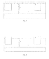
- FIG. 1 shows the structure of a common RFLDMOS. How to reduce the parasitic capacitance in an insulating region to increase the response frequency of the device becomes a major technical difficulty. A common practice to reduce the parasitic capacitance in the insulating region is to greatly increase the thickness of a field oxide film. For the RFLDMOS typically used in 2.4 GHz or higher, the thickness of its oxide film is more than 1 ⁇ m.
- the field oxidation can't be formed by STI process and is usually formed by LOCOS process, which will bring a large unevenness on the substrate after the field oxidation is completed and greatly limit the subsequent process, therefore, the production of small-size devices can't be realized.
- the thickness of the field oxidation is usually more than 1 ⁇ m, typically 2-3 ⁇ m.
- the field oxidation is 0.5 ⁇ m higher than the substrate surface, and for a 0.5 ⁇ m gate, its lithography process window is 0.8 ⁇ 1 ⁇ m.
- the substrate has a large unevenness, making the critical dimension of the device difficult to control and leading to a low yield product and a high production cost of the RFLDMOS. Moreover, based on this structure, the production of a gate below 0.5 ⁇ m is almost impossible. Furthermore, as the field oxidation is usually formed through thermal oxidation, air gaps cannot be formed in isolation regions to further reduce the capacitance, therefore the processing property is also limited.
- An objective of the present invention is to provide an LDMOS device structure and its manufacturing method which can reduce parasitic capacitance, surface unevenness and difficulty of subsequent process and realize the production of small-size gate devices.
- the present invention provides an LDMOS device structure, comprising a MOS transistor cell, wherein an isolation region is formed on each outer side of both a source region and a drain region of the MOS transistor cell; each isolation region formed of silicon dioxide comprises a plurality of isolation trenches and isolates the MOS transistor cell from its surroundings; a height of the isolation region is smaller than or equal to that of the gate of the MOS transistor cell.
- the present invention also provides a manufacturing method of LDMOS device structure, comprising the following steps:
- step 1 forming an isolation layer on a substrate by epitaxy, and then forming a connecting layer connecting to the substrate in the isolation layer by implantation;
- step 2 growing SiO 2 as a hard mask on the isolation layer and then forming a plurality of isolation trenches by dry etching the isolation layer and hard mask;
- step 3 forming isolation regions of SiO 2 , by depleting silicon between the isolation trenches through high temperature drive-in;
- step 4 removing the SiO 2 outside the isolation regions by chemical liquid, and then forming a source, a drain and a gate.
- the present invention can reduce parasitic capacitance, surface unevenness and difficulty of subsequent process and realize the production of small-size gate devices.
- FIG. 1 is a schematic diagram showing the structure of an existing LDMOS device
- FIG. 2 is a schematic diagram showing the structure of an LDMOS device according to the present invention.
- FIG. 3 to FIG. 8 are schematic diagrams showing the steps of the manufacturing method of LDMOS device structure according to the present invention.
- 1 refers to a substrate
- 2 refers to an epitaxial layer
- 3 refers to a connecting layer
- 4 refers to isolation regions
- 5 refers to a source region
- 6 refers to a drain region
- 7 refers to gate oxide
- 8 refers to a gate
- 9 refers to isolation trenches
- 10 refers to silicon dioxide
- 11 refers to a hard mask
- 12 refers to photoresist.
- the present invention discloses an LDMOS device structure.
- the structure includes a MOS transistor cell, wherein an isolation region 4 is formed on each outer side of both a source region 5 and a drain region 6 of the MOS transistor cell; each isolation region 4 formed of silicon dioxide comprises a plurality of isolation trenches 9 and isolates the MOS transistor cell from its surroundings; the height of the isolation region 4 is smaller than or equal to that of a gate 8 of the MOS transistor cell.
- the isolation trenches 9 are deep trenches.
- the present invention also provides a manufacturing method of the LDMOS device structure as shown in FIG. 3 to FIG. 8 , comprising the following steps:
- step 1 as shown in FIG. 3 , forming an isolation layer 2 on a substrate 1 by epitaxy for isolating the device and the substrate 1 , and then forming a connecting layer 3 in the isolation layer 2 by implantation for connecting the device and the substrate 1 ;
- step 2 as shown in FIG. 4 and FIG. 5 , growing SiO 2 as a hard mask 11 and forming a pattern of isolation regions 4 by lithography in a photoresist 12 on the hard mask, and then forming a plurality of isolation trenches 9 by dry etching the isolation layer 2 and hard mask 11 ;
- step 3 as shown in FIG. 6 , forming isolation regions of SiO 2 by depleting silicon between the deep trenches 9 through high temperature drive-in;
- step 4 as shown in FIG. 7 and FIG. 8 , removing SiO 2 10 outside the isolation regions by chemical liquid, and then carrying out subsequent processing to form a source, a drain and a gate.
- the present invention depletes the silicon between the trenches by carrying out high temperature oxidation to a plurality of deep and small-size isolation trenches to form isolation regions with large areas to isolate the RFLDMOS, by which, an isolation structure with a thicker oxide layer can be produced and the isolation with low parasitic capacitances is realized; the height difference between the isolation regions and the active region is greatly reduced to decrease the difficulty of subsequent process, therefore the production of small-size gate devices is realized.
Landscapes
- Engineering & Computer Science (AREA)
- Physics & Mathematics (AREA)
- Condensed Matter Physics & Semiconductors (AREA)
- General Physics & Mathematics (AREA)
- Manufacturing & Machinery (AREA)
- Computer Hardware Design (AREA)
- Microelectronics & Electronic Packaging (AREA)
- Power Engineering (AREA)
- Element Separation (AREA)
- Insulated Gate Type Field-Effect Transistor (AREA)
- Thin Film Transistor (AREA)
Abstract
Description
Claims (4)
Applications Claiming Priority (3)
| Application Number | Priority Date | Filing Date | Title |
|---|---|---|---|
| CN2010105055939A CN102446968A (en) | 2010-10-13 | 2010-10-13 | LDMOS device structure and its fabrication method |
| CN201010505593 | 2010-10-13 | ||
| CN201010505593.9 | 2010-10-13 |
Publications (2)
| Publication Number | Publication Date |
|---|---|
| US20120091524A1 US20120091524A1 (en) | 2012-04-19 |
| US8569833B2 true US8569833B2 (en) | 2013-10-29 |
Family
ID=45933401
Family Applications (1)
| Application Number | Title | Priority Date | Filing Date |
|---|---|---|---|
| US13/271,120 Active US8569833B2 (en) | 2010-10-13 | 2011-10-11 | LDMOS device structure and manufacturing method of the same |
Country Status (2)
| Country | Link |
|---|---|
| US (1) | US8569833B2 (en) |
| CN (1) | CN102446968A (en) |
Families Citing this family (2)
| Publication number | Priority date | Publication date | Assignee | Title |
|---|---|---|---|---|
| US9224858B1 (en) | 2014-07-29 | 2015-12-29 | Globalfoundries Inc. | Lateral double-diffused metal oxide semiconductor field effect transistor (LDMOSFET) with a below source isolation region and a method of forming the LDMOSFET |
| CN108933078B (en) * | 2017-05-25 | 2020-11-03 | 中芯国际集成电路制造(上海)有限公司 | Doping region and forming method and structure of IGBT device |
Citations (3)
| Publication number | Priority date | Publication date | Assignee | Title |
|---|---|---|---|---|
| US5874768A (en) * | 1994-06-15 | 1999-02-23 | Nippondenso Co., Ltd. | Semiconductor device having a high breakdown voltage |
| US20100019311A1 (en) * | 2008-07-22 | 2010-01-28 | Kabushiki Kaisha Toshiba | Semiconductor memory device and manufacturing method thereof |
| US20100203703A1 (en) * | 2005-05-10 | 2010-08-12 | Armin Tilke | Deep Trench Isolation Structures and Methods of Formation Thereof |
-
2010
- 2010-10-13 CN CN2010105055939A patent/CN102446968A/en active Pending
-
2011
- 2011-10-11 US US13/271,120 patent/US8569833B2/en active Active
Patent Citations (3)
| Publication number | Priority date | Publication date | Assignee | Title |
|---|---|---|---|---|
| US5874768A (en) * | 1994-06-15 | 1999-02-23 | Nippondenso Co., Ltd. | Semiconductor device having a high breakdown voltage |
| US20100203703A1 (en) * | 2005-05-10 | 2010-08-12 | Armin Tilke | Deep Trench Isolation Structures and Methods of Formation Thereof |
| US20100019311A1 (en) * | 2008-07-22 | 2010-01-28 | Kabushiki Kaisha Toshiba | Semiconductor memory device and manufacturing method thereof |
Also Published As
| Publication number | Publication date |
|---|---|
| CN102446968A (en) | 2012-05-09 |
| US20120091524A1 (en) | 2012-04-19 |
Similar Documents
| Publication | Publication Date | Title |
|---|---|---|
| US8563370B2 (en) | Method for fabricating surrounding-gate silicon nanowire transistor with air sidewalls | |
| CN105990374B (en) | Integrated circuit and method for making transistors | |
| US9312258B2 (en) | Strained silicon structure | |
| TW200636873A (en) | Semiconductor fabrication process including recessed source/drain regions in an SOI wafer | |
| US9356014B2 (en) | High-voltage metal-insulator-semiconductor field effect transistor structures | |
| US8569833B2 (en) | LDMOS device structure and manufacturing method of the same | |
| CN102903639A (en) | MOS (Metal Oxide Semiconductor) transistor, substrate provided with stress layers and formation method of substrate provided with stress layer | |
| US20150255353A1 (en) | Forming source/drain regions with single reticle and resulting device | |
| CN105336703B (en) | A kind of production method of semiconductor devices | |
| CN103208452A (en) | Metal oxide semiconductor (MOS) transistor and manufacture method thereof | |
| CN103545257A (en) | How to make a CMOS transistor | |
| CN103943678B (en) | A kind of semiconductor devices and its manufacture method | |
| US8722483B2 (en) | Method for manufacturing double-layer polysilicon gate | |
| CN105552126A (en) | Finned-type field effect transistor and fabrication method thereof | |
| CN103151311B (en) | A kind of manufacture method of semiconductor devices | |
| CN103377940A (en) | P-type transmission grid electrode transistor for SRAM and manufacture method thereof | |
| CN102376646B (en) | Method for improving surface morphology of dual-stress nitride | |
| US10186524B2 (en) | Fully depleted silicon-on-insulator (FDSOI) transistor device and self-aligned active area in FDSOI bulk exposed regions | |
| US8669616B2 (en) | Method for forming N-shaped bottom stress liner | |
| US9059202B2 (en) | Metal-oxide-semiconductor (MOS) device and method for fabricating the same | |
| CN110556341B (en) | Method for manufacturing semiconductor device | |
| CN111370313B (en) | NMOS device preparation method | |
| CN102487017A (en) | Manufacturing method of strain CMOS device | |
| CN104319256A (en) | Isolation structure of narrow active region and manufacturing method thereof | |
| CN103531468B (en) | A kind of MOS transistor and preparation method thereof |
Legal Events
| Date | Code | Title | Description |
|---|---|---|---|
| AS | Assignment |
Owner name: SHANGHAI HUA HONG NEC ELECTRONICS CO., LTD., CHINA Free format text: ASSIGNMENT OF ASSIGNORS INTEREST;ASSIGNORS:ZHANG, SHUAI;WANG, HAIJUN;REEL/FRAME:027045/0626 Effective date: 20110729 |
|
| STCF | Information on status: patent grant |
Free format text: PATENTED CASE |
|
| AS | Assignment |
Owner name: SHANGHAI HUAHONG GRACE SEMICONDUCTOR MANUFACTURING Free format text: MERGER;ASSIGNOR:SHANGHAI HUA HONG NEC ELECTRONICS CO., LTD.;REEL/FRAME:032885/0047 Effective date: 20130124 |
|
| FEPP | Fee payment procedure |
Free format text: PAYOR NUMBER ASSIGNED (ORIGINAL EVENT CODE: ASPN); ENTITY STATUS OF PATENT OWNER: LARGE ENTITY |
|
| FPAY | Fee payment |
Year of fee payment: 4 |
|
| MAFP | Maintenance fee payment |
Free format text: PAYMENT OF MAINTENANCE FEE, 8TH YEAR, LARGE ENTITY (ORIGINAL EVENT CODE: M1552); ENTITY STATUS OF PATENT OWNER: LARGE ENTITY Year of fee payment: 8 |
|
| MAFP | Maintenance fee payment |
Free format text: PAYMENT OF MAINTENANCE FEE, 12TH YEAR, LARGE ENTITY (ORIGINAL EVENT CODE: M1553); ENTITY STATUS OF PATENT OWNER: LARGE ENTITY Year of fee payment: 12 |