US8414355B2 - Substrate processing apparatus - Google Patents
Substrate processing apparatus Download PDFInfo
- Publication number
- US8414355B2 US8414355B2 US12/458,814 US45881409A US8414355B2 US 8414355 B2 US8414355 B2 US 8414355B2 US 45881409 A US45881409 A US 45881409A US 8414355 B2 US8414355 B2 US 8414355B2
- Authority
- US
- United States
- Prior art keywords
- substrate
- image
- polishing
- wafer
- periphery
- Prior art date
- Legal status (The legal status is an assumption and is not a legal conclusion. Google has not performed a legal analysis and makes no representation as to the accuracy of the status listed.)
- Active, expires
Links
- 239000000758 substrate Substances 0.000 title claims abstract description 153
- 238000012545 processing Methods 0.000 title claims abstract description 105
- 238000005498 polishing Methods 0.000 claims abstract description 241
- 238000003384 imaging method Methods 0.000 claims abstract description 125
- 230000007246 mechanism Effects 0.000 claims description 64
- 238000000034 method Methods 0.000 claims description 54
- 238000007689 inspection Methods 0.000 claims description 34
- 230000003287 optical effect Effects 0.000 claims description 23
- 238000003860 storage Methods 0.000 claims description 10
- 238000012805 post-processing Methods 0.000 claims description 7
- 235000012431 wafers Nutrition 0.000 description 279
- XLYOFNOQVPJJNP-UHFFFAOYSA-N water Substances O XLYOFNOQVPJJNP-UHFFFAOYSA-N 0.000 description 22
- 238000004140 cleaning Methods 0.000 description 16
- 238000007517 polishing process Methods 0.000 description 14
- 238000001035 drying Methods 0.000 description 13
- 230000008569 process Effects 0.000 description 13
- 210000000078 claw Anatomy 0.000 description 10
- 238000004891 communication Methods 0.000 description 9
- 238000011084 recovery Methods 0.000 description 8
- 238000010521 absorption reaction Methods 0.000 description 6
- 238000001514 detection method Methods 0.000 description 6
- 230000006870 function Effects 0.000 description 6
- 239000007788 liquid Substances 0.000 description 6
- 239000000463 material Substances 0.000 description 6
- 230000003746 surface roughness Effects 0.000 description 6
- XUIMIQQOPSSXEZ-UHFFFAOYSA-N Silicon Chemical compound [Si] XUIMIQQOPSSXEZ-UHFFFAOYSA-N 0.000 description 5
- 239000003086 colorant Substances 0.000 description 5
- 229910052710 silicon Inorganic materials 0.000 description 5
- 239000010703 silicon Substances 0.000 description 5
- 230000008859 change Effects 0.000 description 4
- 230000003028 elevating effect Effects 0.000 description 4
- 239000012530 fluid Substances 0.000 description 4
- 230000001965 increasing effect Effects 0.000 description 4
- 230000033001 locomotion Effects 0.000 description 4
- 238000005259 measurement Methods 0.000 description 4
- 230000010355 oscillation Effects 0.000 description 4
- 238000003672 processing method Methods 0.000 description 4
- 238000012546 transfer Methods 0.000 description 4
- 239000006061 abrasive grain Substances 0.000 description 3
- 238000010586 diagram Methods 0.000 description 3
- 238000011065 in-situ storage Methods 0.000 description 3
- VYPSYNLAJGMNEJ-UHFFFAOYSA-N Silicium dioxide Chemical compound O=[Si]=O VYPSYNLAJGMNEJ-UHFFFAOYSA-N 0.000 description 2
- 229910003460 diamond Inorganic materials 0.000 description 2
- 239000010432 diamond Substances 0.000 description 2
- 238000005530 etching Methods 0.000 description 2
- 239000011347 resin Substances 0.000 description 2
- 229920005989 resin Polymers 0.000 description 2
- 239000004065 semiconductor Substances 0.000 description 2
- 230000009471 action Effects 0.000 description 1
- 239000011248 coating agent Substances 0.000 description 1
- 238000000576 coating method Methods 0.000 description 1
- 229910052681 coesite Inorganic materials 0.000 description 1
- 238000011109 contamination Methods 0.000 description 1
- 238000001816 cooling Methods 0.000 description 1
- 229910052906 cristobalite Inorganic materials 0.000 description 1
- 230000004069 differentiation Effects 0.000 description 1
- 239000013013 elastic material Substances 0.000 description 1
- 239000004744 fabric Substances 0.000 description 1
- 229910021645 metal ion Inorganic materials 0.000 description 1
- 238000012986 modification Methods 0.000 description 1
- 230000004048 modification Effects 0.000 description 1
- 239000013307 optical fiber Substances 0.000 description 1
- 239000002245 particle Substances 0.000 description 1
- 230000002093 peripheral effect Effects 0.000 description 1
- 238000003825 pressing Methods 0.000 description 1
- 238000005201 scrubbing Methods 0.000 description 1
- 238000005389 semiconductor device fabrication Methods 0.000 description 1
- 239000000377 silicon dioxide Substances 0.000 description 1
- 229910052682 stishovite Inorganic materials 0.000 description 1
- 239000000126 substance Substances 0.000 description 1
- 229910052905 tridymite Inorganic materials 0.000 description 1
- 229910021642 ultra pure water Inorganic materials 0.000 description 1
- 239000012498 ultrapure water Substances 0.000 description 1
Images


Classifications
-
- B—PERFORMING OPERATIONS; TRANSPORTING
- B24—GRINDING; POLISHING
- B24B—MACHINES, DEVICES, OR PROCESSES FOR GRINDING OR POLISHING; DRESSING OR CONDITIONING OF ABRADING SURFACES; FEEDING OF GRINDING, POLISHING, OR LAPPING AGENTS
- B24B9/00—Machines or devices designed for grinding edges or bevels on work or for removing burrs; Accessories therefor
- B24B9/02—Machines or devices designed for grinding edges or bevels on work or for removing burrs; Accessories therefor characterised by a special design with respect to properties of materials specific to articles to be ground
- B24B9/06—Machines or devices designed for grinding edges or bevels on work or for removing burrs; Accessories therefor characterised by a special design with respect to properties of materials specific to articles to be ground of non-metallic inorganic material, e.g. stone, ceramics, porcelain
- B24B9/065—Machines or devices designed for grinding edges or bevels on work or for removing burrs; Accessories therefor characterised by a special design with respect to properties of materials specific to articles to be ground of non-metallic inorganic material, e.g. stone, ceramics, porcelain of thin, brittle parts, e.g. semiconductors, wafers
-
- B—PERFORMING OPERATIONS; TRANSPORTING
- B24—GRINDING; POLISHING
- B24B—MACHINES, DEVICES, OR PROCESSES FOR GRINDING OR POLISHING; DRESSING OR CONDITIONING OF ABRADING SURFACES; FEEDING OF GRINDING, POLISHING, OR LAPPING AGENTS
- B24B21/00—Machines or devices using grinding or polishing belts; Accessories therefor
- B24B21/004—Machines or devices using grinding or polishing belts; Accessories therefor using abrasive rolled strips
-
- B—PERFORMING OPERATIONS; TRANSPORTING
- B24—GRINDING; POLISHING
- B24B—MACHINES, DEVICES, OR PROCESSES FOR GRINDING OR POLISHING; DRESSING OR CONDITIONING OF ABRADING SURFACES; FEEDING OF GRINDING, POLISHING, OR LAPPING AGENTS
- B24B37/00—Lapping machines or devices; Accessories
- B24B37/005—Control means for lapping machines or devices
- B24B37/013—Devices or means for detecting lapping completion
-
- B—PERFORMING OPERATIONS; TRANSPORTING
- B24—GRINDING; POLISHING
- B24B—MACHINES, DEVICES, OR PROCESSES FOR GRINDING OR POLISHING; DRESSING OR CONDITIONING OF ABRADING SURFACES; FEEDING OF GRINDING, POLISHING, OR LAPPING AGENTS
- B24B49/00—Measuring or gauging equipment for controlling the feed movement of the grinding tool or work; Arrangements of indicating or measuring equipment, e.g. for indicating the start of the grinding operation
- B24B49/12—Measuring or gauging equipment for controlling the feed movement of the grinding tool or work; Arrangements of indicating or measuring equipment, e.g. for indicating the start of the grinding operation involving optical means
Definitions
- the present invention relates to a substrate processing apparatus having a polishing unit for polishing a periphery of a substrate, and more particularly to a substrate processing apparatus having a mechanism for inspecting a polished surface.
- polishing apparatus having multiple polishing modules arranged so as to surround a substrate.
- This type of polishing apparatus realizes a high throughput by operating the multiple polishing modules simultaneously to polish a periphery of the rotating substrate.
- the polishing apparatus has a module for detecting an end point of polishing of a substrate. Examples of such a polishing-end-point detection module include a so-called in-situ polishing-end-point detection module which is incorporated in the polishing apparatus.
- the polishing-end-point detection module of in-situ type is generally designed to monitor a film on the periphery of the substrate while the polishing modules are polishing the periphery of the substrate, and determine the polishing end point based on a time when the film is removed. Therefore, it is necessary to arrange the polishing-end-point detection module next to the polishing modules. However, since the plural polishing modules access the substrate during polishing of the substrate, there is no space for the polishing-end-point detection module to access the substrate. Moreover, in view of the fact that the high-throughput polishing apparatus polishes each substrate in several seconds, it becomes meaningless to detect the polishing end point during polishing.
- a polishing liquid typically pure water
- a polishing liquid which is supplied to the substrate during polishing, can hinder the polishing-end-point detecting operation of the polishing-end-point detection module.
- a polishing liquid typically pure water
- the transparent tape is brought into contact with the periphery of the substrate while advancing the transparent tape, and polishing of the periphery of the substrate is monitored from the back of the transparent tape.
- this solution requires a highly-transparent tape and thus entails an increased cost.
- the present invention has been made in view of the above drawbacks. It is therefore an object of the present invention to provide a substrate processing apparatus having a low-cost polished-state inspection unit suitable for use with a high-throughput polishing unit.
- One aspect of the present invention for achieving the above object is to provide a substrate processing apparatus including: a polishing unit configured to polish a periphery of a substrate; an imaging module configured to take an image of the periphery of the substrate polished by the polishing unit; and an image processing section configured to inspect a polished state of the substrate based on the image taken by the imaging module.
- the imaging module is configured to take the image of the periphery of the substrate when the polishing unit is not polishing the periphery of the substrate.
- the substrate processing apparatus further includes a polishing-condition determining section configured to determine a polishing condition in the polishing unit.
- An inspection result of the image processing section is transmitted to the polishing-condition determining section, and the polishing-condition determining section determines the polishing condition in the polishing unit based on the inspection result.
- the imaging module is configured to take the image of the periphery of the substrate from multiple directions.
- the imaging module includes a prism disposed adjacent to the periphery of the substrate and an imaging camera for taking the image of the periphery of the substrate through the prism.
- the imaging module includes plural imaging cameras.
- the image processing section is configured to inspect the polished state of the substrate based on a color of the image taken by the imaging module.
- the image processing section is configured to quantify the color of the image taken by the imaging module to express the image in a numerical value, and further configured to determine that an object has been removed from the periphery when the numerical value is larger than or smaller than a preset threshold.
- the substrate processing apparatus further includes a substrate holding rotary mechanism for rotating the substrate about its own central axis.
- the imaging module is disposed adjacent to the periphery of the substrate held by the substrate holding rotary mechanism, and the imaging module is configured to take the image of the periphery of the substrate while the substrate holding rotary mechanism rotates the substrate intermittently or continuously.
- the imaging module is configured to take a still image of the periphery of the substrate.
- the imaging module is configured to take an accumulated image of the periphery of the substrate.
- the imaging module has a line scan camera.
- the imaging module has multiple cameras with different fields of view.
- the substrate processing apparatus further includes a measuring unit configured to measure a predetermined physical quantity of the substrate polished by the polishing unit.
- the imaging module is incorporated in the measuring unit.
- the measuring unit has a substrate holding rotary mechanism for rotating the substrate about its own central axis, and the imaging module is disposed adjacent to the periphery of the substrate held by the substrate holding rotary mechanism.
- the substrate processing apparatus further includes at least one post-processing unit configured to perform a post-process on the substrate polished by the polishing unit.
- the imaging module is incorporated in the at least one post-processing unit.
- the at least one post-processing unit has a substrate holding rotary mechanism for rotating the substrate about its own central axis, and the imaging module is disposed adjacent to the periphery of the substrate held by the substrate holding rotary mechanism.
- the substrate processing apparatus further includes a storage device for storing an inspection result of the image processing section.
- the substrate processing apparatus further includes: a storage device for storing the image taken by the imaging module; and an image display device for displaying the image stored in the storage device.
- the storage device stores the image and information indicating a position where the image was taken, and the image display device is configured to display an image in a position requested.
- Another aspect of the present invention is to provide a substrate processing method including: polishing a periphery of a substrate; taking an image of the periphery of the substrate when the polishing of the periphery of the substrate is not performed; and inspecting a polished state of the substrate based on the image.
- the present invention as described above can provide a so-called in-line inspection unit which can inspect the polished-state of the substrate independently of the polishing process after the polishing process is completed or after the polishing process is stopped temporarily. Therefore, the inspection is not affected by a polishing liquid (e.g., pure water) and a transparent tape is not required.
- This polished-state inspection unit of in-line type can be installed outside of the polishing unit. This arrangement does not necessitate a change in structure of the polishing unit. Therefore, the structure of the high-throughput polishing unit can be used as it is.
- FIG. 1A and FIG. 1B are enlarged cross-sectional views each showing a periphery of a substrate, such as a semiconductor wafer;
- FIG. 2 is a schematic plan view showing a whole structure of a substrate processing apparatus according to an embodiment of the present invention
- FIG. 3A is a schematic perspective view showing a substrate holding rotary mechanism provided in a measuring unit
- FIG. 3B is a schematic plan view showing the substrate holding rotary mechanism
- FIG. 4A and FIG. 4B are views illustrating operations of the substrate holding rotary mechanism
- FIG. 5 is a schematic perspective view showing the measuring unit
- FIG. 6A is a schematic plan view of the measuring unit
- FIG. 6B is a view from a direction as indicated by arrow VI in FIG. 6A ;
- FIG. 7 is a schematic cross-sectional view showing a first polishing unit
- FIG. 8A through FIG. 8C are views illustrating motions of a bevel polishing head during polishing of a bevel portion
- FIG. 9 is a schematic view showing a polished-state inspection unit
- FIG. 10 is a schematic view illustrating optical paths of images
- FIG. 11 is a view showing an example of image-pickup positions of a wafer in a step-and-repeat method
- FIG. 12 is a flowchart showing operation sequence of the step-and-repeat method
- FIG. 13A and FIG. 13B are views each showing an example of image-pickup positions of a wafer in a scan method
- FIG. 14 is a flowchart showing operation sequence of the scan method
- FIG. 15 is a view illustrating five regions defined on the bevel portion of the wafer.
- FIG. 16 is a schematic view illustrating images of the periphery of the wafer taken by an imaging module
- FIG. 17 is a view showing a color chart and a brightness chart for use in setting of a target color
- FIG. 18 is a diagram illustrating a film-removal determining process in a case where a color of silicon is selected as the target color
- FIG. 19 is a diagram illustrating a film-removal determining process in a case where a color of a film to be removed is selected as the target color;
- FIG. 20A is a schematic view showing an image of the periphery of the wafer with a rough surface and showing the image that has been subjected to a differential processing;
- FIG. 20B is a histogram that numerically expresses the image shown in FIG. 20A ;
- FIG. 21A is a schematic view showing an image of the periphery of the wafer with a smooth surface and showing the image that has been subjected to a differential processing;
- FIG. 21B is a histogram that numerically expresses the image shown in FIG. 21A ;
- FIG. 22 is a view showing a modified example of the imaging module
- FIG. 23A is a schematic view showing another modified example of the imaging module.
- FIG. 23B is a schematic view showing a region taken by a second imaging module.
- FIG. 1A and FIG. 1B are enlarged cross-sectional views each showing a periphery of a substrate, such as a semiconductor wafer (which will be hereinafter referred to simply as “wafer”). More specifically, FIG. 1A shows a cross-sectional view of a so-called straight-type wafer W having a periphery whose cross section is constituted by straight lines, and FIG. 1B shows a so-called round-type wafer W having a periphery whose cross section is constituted by curved lines.
- a substrate such as a semiconductor wafer
- a bevel portion is an area B that is constituted by an upper slope (an upper bevel portion) P, a lower slope (a lower bevel portion) Q, and a side portion (an apex) R.
- a bevel portion is an area B that forms a circumferential surface of the wafer W and has a curved cross section.
- a near-edge portion is an area located radially inwardly of the bevel portion B of the wafer W and is indicated by flat portions E 1 and E 2 located radially outwardly of an area D where devices are formed.
- the periphery of the wafer means a region including the bevel portion B and the near-edge portions E 1 and E 2 .
- the upper near-edge portion E 1 is referred to as a top near-edge portion and the lower near-edge portion E 2 is referred to as a back near-edge portion.
- FIG. 2 is a schematic plan view showing a whole structure of a substrate processing apparatus according to an embodiment of the present invention.
- the substrate processing apparatus 1 shown in FIG. 2 includes a load-unload port 10 in which wafer supply-recovery devices 11 A and 11 B are installed, a measuring unit 30 for measuring a diameter of a wafer, and a first transfer robot 20 A for transporting a wafer mainly between the load-unload port 10 , the measuring unit 30 , and a secondary cleaning-drying unit 110 which will be discussed later.
- the substrate processing apparatus 1 further includes a first polishing unit 70 A and a second polishing unit 70 B for polishing the periphery of the wafer, a primary cleaning unit 100 for performing a primary cleaning process on the polished wafer, the secondary cleaning-drying unit 110 for performing a secondary cleaning process on the primarily-cleaned wafer and performing a drying process on the secondarily-cleaned wafer, and a second transfer robot 20 B for transporting the wafer mainly between the first and second polishing units 70 A and 70 B, the primary cleaning unit 100 , and the secondary cleaning-drying unit 110 .
- the substrate processing apparatus 1 further includes a polishing-condition determining section 120 for determining polishing conditions in the first and second polishing units 70 A and 70 B based on a measurement result of the wafer in the measuring unit 30 .
- the polishing-condition determining section 120 is part of a controller and is a calculator for calculating the polishing conditions based on the measurement result of the periphery of the wafer.
- Every unit of the substrate processing apparatus 1 is arranged in a housing 3 which is installed in a clean room 2 .
- An interior space of the clean room 2 and an interior space of the substrate processing apparatus 1 are partitioned by the housing 3 .
- a non-illustrated filter is provided on a top of the housing 3 , so that a clean air is introduced into the housing 3 to form downflow of the clean air therein and is expelled to the exterior of the housing 3 through an exhaust port (not shown in the drawing) provided on a bottom of the housing 3 .
- the air flow in the substrate processing apparatus 1 is controlled so as to be suited for the substrate processing.
- the units in the housing 3 are further housed in housings, respectively, so that air flow in each housing is controlled so as to be suited for the substrate processing.
- the load-unload port 10 is installed outwardly of a side wall 3 a that is located adjacent to the first transfer robot 20 A.
- the two wafer supply-recovery devices 11 A and 11 B are disposed in parallel.
- the wafer supply-recovery devices 11 A and 11 B are referred to as FOUP (Front Opening Unified Pod) configured to supply and recover a wafer (i.e., an object to be processed) to and from the substrate processing apparatus.
- FOUP Front Opening Unified Pod
- a wafer cassette (or wafer carrier) 12 A or 12 B which houses plural wafers therein, is placed onto the wafer supply-recovery device 11 A or 11 B, a lid of the wafer cassette 12 A or 12 B is opened automatically and a window (not shown) on the side wall 3 a is opened, so that the first transfer robot 20 A can remove a wafer from the wafer cassette 12 A or 12 B and transport the wafer into the substrate processing apparatus 1 .
- FIG. 3A is a schematic perspective view showing a substrate holding rotary mechanism provided in the measuring unit 30 which will be discussed later
- FIG. 3B is a schematic plan view showing the substrate holding rotary mechanism.
- the substrate holding rotary mechanism 61 is a device for holding and rotating the wafer W when the measuring unit 30 is performing its measuring operation.
- the substrate holding rotary mechanism 61 includes an upper chuck (or upper spin chuck) 62 with plural claws 62 a for holding the periphery of the wafer W and a lower chuck (or lower spin chuck) 63 with plural claws 63 a for holding the periphery of the wafer W similarly.
- the upper chuck 62 and the lower chuck 63 are arranged concentrically and are rotatable about a rotational shaft 64 .
- the claws 62 a and 63 a of the upper and lower chucks 62 and 63 are three or four claws arranged at predetermined intervals.
- the lower chuck 63 is movable vertically by a non-illustrated elevating mechanism.
- the substrate holding rotary mechanism 61 further includes a stepping motor as a rotating device for rotating the upper chuck 62 and the lower chuck 63 and a rotary encoder as a rotational position detector for detecting a rotational position or a rotational angle of the wafer W, as will be described later.
- the upper chuck 62 holds and rotates the wafer W when measuring the diameter of the wafer W.
- the claw 62 a can reach a measuring position of the periphery of the wafer W.
- the lower chuck 63 is elevated to hold the wafer W as shown in FIG. 4B , whereby the wafer W is separated from the upper chuck 62 .
- the upper chuck 62 is rotated through a predetermined angle, so that the claw 62 a can avoid overlapping the measuring position.
- the lower chuck 63 is lowered to allow the upper chuck 62 to hold the wafer W again. Because these operations can prevent the claws 62 a of the upper chuck 62 from overlapping the measuring position, the diameter of the wafer W can be measured over the periphery of the wafer W in its entirety.
- FIG. 5 is a schematic perspective view showing the measuring unit 30 .
- FIG. 6A is a schematic plan view of the measuring unit 30
- FIG. 6B is a view from a direction as indicated by arrow VI in FIG. 6A .
- the substrate holding rotary mechanism 61 is not depicted.
- This measuring unit 30 has a diameter-measuring device configured to measure a dimension (i.e., a diameter) of the wafer W and is provided for determining from the measured diameter an amount of material removed from the side portion of the wafer W by the polishing process.
- the measuring unit 30 includes the substrate holding rotary mechanism 61 and sensor devices (laser sensors) 31 and 31 each having a pair of a light emitter 32 and a light receiver 33 arranged at their predetermined positions above and below the periphery of the wafer W held by the substrate holding rotary mechanism 61 .
- the light emitter 32 is a device that emits laser light.
- the two sensor devices 31 and 31 are provided. These sensor devices 31 and 31 are arranged in symmetric positions on a center line of the wafer W held by the substrate holding rotary mechanism 61 .
- the sensor devices 31 and 31 are coupled to a data processor (not shown), which is configured to quantify amounts of the laser lights received by the light receivers 33 and 33 and process the quantified amounts of the laser lights.
- the light receivers 33 and 33 may be located above the wafer W and the light emitters 32 and 32 may be located below the wafer W.
- the light emitters 32 and 32 of the sensor devices 31 and 31 emit the laser lights 34 and 34 downwardly toward the periphery of the wafer W.
- the laser lights 34 and 34 are a liner light (or a sheet-shaped light) with a predetermined width.
- Each laser light 34 impinges upon the periphery of the wafer W along the radial direction thereof and part of the laser light 34 is interrupted by an upper surface of the periphery of the wafer W. Therefore, the other part of the laser light 34 , which is not interrupted by the wafer W and has traveled outwardly of the wafer W, is received by the light receiver 33 .
- the data processor quantifies or expresses numerically the amounts of the laser lights 34 and 34 received by the light receivers 33 and 33 to determine widths of the laser lights 34 and 34 that have traveled through the periphery of the wafer W, i.e., measure dimensions of D 1 and D 2 shown in FIG. 6B .
- a reference wafer (not shown) with a known diameter is prepared, and the dimensions of D 1 and D 2 with respect to the reference wafer are measured in advance by the measuring unit 30 .
- the diameter Dw of the wafer W (i.e., a wafer to be measured) can be determined from a difference between the dimensions D 1 and D 2 of the reference wafer and the dimensions D 1 and D 2 of the wafer W and the known diameter of the reference wafer.
- the diameter of the wafer W can be measured at different points on the periphery of the wafer W by changing the rotational position (i.e., orientation) of the wafer W by the upper chuck 62 and the lower chuck 63 of the substrate holding rotary mechanism 61 . With this operation, information (e.g., variation in an amount of material removed from the periphery of the wafer W), which is not available by single-point measurement, can be obtained. Further, the diameter of the wafer W can be measured continuously with the wafer W being rotated by the substrate holding rotary mechanism 61 . According to this measuring method, the measurement data of the diameter can be obtained as continuous data. Therefore, roundness of the wafer can be determined.
- FIG. 7 is a schematic cross-sectional view showing the first polishing unit. As shown in FIG. 7 , the first polishing unit 70 A has a housing 71 in which components of the polishing unit 70 A are housed.
- the first polishing unit 70 A includes a substrate holding rotary section 72 for holding a rear surface of the wafer W by a vacuum suction, a substrate-transferring mechanism 80 for performing centering and transferring of the wafer W, a bevel polishing section 83 for polishing the bevel portion of the wafer W, and a notch polishing section 90 for polishing a notch portion of the wafer W.
- the substrate holding rotary section 72 has, as shown in FIG. 7 , a substrate-holding table 73 having an upper surface with grooves 73 a for attracting the wafer W by the vacuum suction, and a support shaft 74 that supports the substrate-holding table 73 .
- a rotating device (i.e., a stage-rotating device) 75 is coupled to the support shaft 74 , so that the substrate-holding table 73 and the support shaft 74 are rotated in unison by the rotating device 75 .
- the grooves 73 a of the substrate-holding table 73 are in fluid communication with a communication passage 73 b formed in the substrate-holding table 73 , and the communication passage 73 b is in fluid communication with a communication passage 74 a formed in the support shaft 74 .
- the communication passage 74 a is coupled to a vacuum line 76 and a compressed-air supply line 77 .
- a non-illustrated elevating mechanism is coupled to the substrate-holding table 73 and the support shaft 74 . The substrate-holding table 73 is moved in the vertical direction by this elevating mechanism.
- An absorption pad 78 which is made of an elastic material (e.g., urethane-base material), is attached to the upper surface of the substrate-holding table 73 so as to cover the grooves 73 a .
- This absorption pad 78 has a number of through-holes (not shown) each having a small diameter. These through-holes are in fluid communication with the grooves 73 a of the substrate-holding table 73 . Therefore, when the fluid communication is established between the vacuum line 76 and the communication passage 74 a , the vacuum is developed in the through-holes of the absorption pad 78 , and the wafer W on the absorption pad 78 is attracted to an upper surface of the absorption pad 78 due to the vacuum suction.
- This absorption pad 78 has the function of producing the vacuum between the wafer W and the substrate-holding table 73 and the function of reducing an impact on the wafer W when the wafer W is placed onto the substrate-holding table 73 .
- the substrate-transferring mechanism 80 is located above the substrate holding rotary section 72 .
- the substrate-transferring mechanism 80 has a pair of arms 81 and 81 .
- Plural cylindrical members 82 each having a recessed surface corresponding to the bevel portion of the wafer W, are secured to the respective arms 81 and 81 .
- the arms 81 and 81 are movable toward and away from each other and can stop at a close position and an open position.
- the arms 81 and 81 hold the wafer W with the cylindrical members 82 at the close position and release the wafer W at the open position.
- centering of the wafer W is conducted.
- the substrate-holding table 73 is elevated by the elevating mechanism to receive the wafer W from the substrate-transferring mechanism 80 , and holds the wafer W thereon by the vacuum suction and is lowered to a polishing position.
- the bevel polishing section 83 includes a bevel polishing head 85 configured to press a polishing tape 84 against the bevel portion of the wafer W, and a polishing-tape feeding mechanism 88 .
- This polishing-tape feeding mechanism 88 includes a supply reel 88 a for supplying the polishing tape 84 to the bevel polishing head 85 and a recovery reel 88 b for recovering the polishing tape 84 from the bevel polishing head 85 .
- the bevel polishing head 85 has a pair of guide rollers 86 and 86 on which the polishing tape 84 rides so as to face the substrate-holding table 73 .
- the polishing tape 84 extends in tension between the guide rollers 86 and 86 , and the bevel polishing head 85 brings a polishing surface 84 a of the polishing tape 84 into contact with the bevel portion of the wafer W.
- a base 87 is provided at the back of the polishing tape 84 extending between the guide rollers 86 and 86 . This base 87 has a contact surface that is brought into contact with the polishing tape 84 .
- an elastic member may be attached to the contact surface of the base 87 .
- the bevel polishing head 85 is movable in the radial direction of the wafer W by a non-illustrated moving mechanism.
- the polishing surface 84 a of the polishing tape 84 is pressed against the bevel portion of the wafer W by a combination of an action of the base 87 that presses the polishing tape 84 from behind and the tension of the polishing tape 84 itself.
- the polishing tape 84 is a band-shaped member with a constant width and has a length of several tens of meters.
- the polishing tape 84 is wound on a cylindrical core 89 . This core 89 is attached to the supply reel 88 a .
- the polishing tape 84 extends between the pair of the guide rollers 86 and 86 of the bevel polishing head 85 with the polishing surface 84 a facing outward.
- One end of the polishing tape 84 is attached to the recovery reel 88 b .
- a non-illustrated rotating mechanism such as a motor, is coupled to the recovery reel 88 b , so that the polishing tape 84 is wound and recovered with a predetermined tension applied by the rotating mechanism.
- the polishing surface 84 a of the polishing tape 84 is manufactured by coating one surface of a tape base with a resin material containing abrasive grains dispersed therein and then solidifying the resin material.
- Diamond or SiC may be used as the abrasive grains.
- Type and grain size of the abrasive grains are selected according to the type of the wafer to be polished and a polishing degree required. For example, diamond with a grain size in a range of #4000 to #20000 or SiC with a grain size in a range of #4000 to #10000 can be used.
- a band-shaped polishing cloth having a polishing surface with no grains attached may be used.
- different types of polishing tapes may be set in the first polishing unit 70 A and the second polishing unit 70 B, respectively. In this case, different polishing processes can be performed.
- FIG. 8A through FIG. 8C are views illustrating motions of the bevel polishing head 85 during polishing of the bevel portion.
- the bevel polishing section 83 has an oscillation mechanism for causing the bevel polishing head 85 to oscillate vertically about a polishing point on the bevel portion of the wafer W, so that the polishing surface 84 a of the polishing tape 84 can contact the bevel portion with the polishing head 85 inclined vertically at a predetermined angle with respect to the wafer surface. Therefore, as shown in FIG. 8A , the upper slope of the bevel portion and the top near-edge portion can be polished by inclining the polishing head 85 upwardly at predetermined angles with respect to the wafer surface. Similarly, as shown in FIG.
- the side portion of the bevel portion can be polished by keeping the polishing head 85 horizontally, and as shown in FIG. 8C , the lower slope of the bevel portion and the back near-edge portion can be polished by inclining the polishing head 85 downwardly at predetermined angles with respect to the wafer surface. Further, the upper and lower slopes and the side portion of the bevel portion, and the boundaries thereof can be polished to have desired angles and shapes by fine adjustment of the tilt angle of the bevel polishing head 85 .
- the notch polishing section 90 includes a notch polishing head 92 configured to press a polishing tape 91 against the notch portion of the wafer W, and a polishing-tape feeding mechanism 94 .
- the notch polishing head 92 is movable in the radial direction of the wafer W by a non-illustrated moving mechanism.
- the polishing-tape feeding mechanism 94 includes a supply reel 94 a for supplying the polishing tape 91 to the notch polishing head 92 and a recovery reel 94 b for recovering the polishing tape 91 from the notch polishing head 92 .
- the notch polishing head 92 has a pair of guide rollers 93 and 93 on which the polishing tape 91 rides.
- the polishing tape 91 extends in tension between the guide rollers 93 and 93 , and the notch polishing head 92 brings a polishing surface 91 a of the polishing tape 91 into contact with the notch portion of the wafer W.
- the polishing tape 91 to be used in the notch polishing section 90 is made of the same material as the polishing tape 84 used in the bevel polishing section 83 .
- the polishing tape 91 has a width that corresponds to a shape of the notch portion of the wafer W.
- the width of the polishing tape 91 for use in the notch polishing section 90 is smaller than the width of the polishing tape 84 for use in the bevel polishing section 83 .
- the notch polishing section 90 has an oscillation mechanism (not shown in the drawing and not described in detail herein) for causing the notch polishing head 92 to oscillate vertically about a polishing point on the notch portion of the wafer W, so that the polishing surface 91 a of the polishing tape 91 can contact the notch portion with the notch polishing head 92 inclined at a predetermined angle with respect to the wafer surface during polishing. Therefore, the notch polishing head 92 can polish the notch portion along its surface shape, and can also polish the notch portion to desired angle and shape.
- the notch polishing section 90 further includes a notch detecting device (not shown) for detecting the notch portion of the wafer W.
- the first polishing unit 70 A has, as shown in FIG. 7 , polishing-water supply nozzles 95 and 96 for supplying water (i.e., polishing water), such as ultrapure water, onto the upper surface and the lower surface of the wafer W at positions near the polishing points. Further, the first polishing unit 70 A has a polishing-water supply nozzle 97 for supplying the polishing water onto the center of the upper surface of the wafer W. This polishing-water supply nozzle 97 is located above the substrate-holding table 73 .
- polishing water from the polishing-water supply nozzles 95 and 96 during polishing of the bevel portion and the notch portion can prevent polishing debris (i.e., particles produced by the polishing process) from adhering to the upper surface and the lower surface of the wafer W.
- the polishing water from the polishing-water supply nozzle 97 is supplied toward the center of the wafer W, and flows from the center to the periphery of the wafer W by the rotation of the wafer W. This flow of the polishing water serves to sweep away the polishing debris to the periphery of the wafer W.
- the lower polishing-water supply nozzle 96 supplies the polishing water onto an exposed portion of the lower surface of the wafer W that is located outwardly of the substrate-holding table 73 . By supplying the polishing water onto the exposed portion of the wafer W, the polishing water can flow toward the periphery of the wafer W by the rotation of the wafer W to thereby carry the polishing debris to the periphery of the wafer W.
- the polishing water supplied from the polishing-water supply nozzles 95 and 96 , not only has the function of preventing contamination of the upper and lower surfaces of the wafer W due to the polishing debris, but also has the cooling function of removing heat generated by friction during polishing of the wafer W. Therefore, heat of the polished portion of the wafer W can be removed by adjusting a temperature of the polishing water to be supplied. Consequently, a stable polishing operation can be performed.
- the wafer W to be polished, is carried into the housing 71 and transported to the substrate-transferring mechanism 80 .
- the arms 81 and 81 of the substrate-transferring mechanism 80 are closed to hold the wafer W, whereby centering of the wafer W is performed.
- the substrate-holding table 73 is elevated to the position of the substrate-transferring mechanism 80 , and attracts the wafer W, held by the arms 81 and 81 , by the vacuum suction.
- the arms 81 and 81 are opened to release the wafer W, whereby the wafer W is held on the upper surface of the substrate-holding table 73 .
- the substrate-holding table 73 holding the wafer W, is lowered to the polishing position as shown in FIG. 7 .
- the rotating device 75 is set in motion to rotate the wafer W together with the substrate-holding table 73 .
- the supply reel 88 a of the bevel polishing section 83 supplies the polishing tape 84 to the bevel polishing head 85 to set an unused polishing surface 84 a between the guide rollers 86 and 86 of the bevel polishing head 85 .
- the bevel polishing head 85 is moved toward the wafer W by the moving mechanism to bring the polishing surface 84 a of the polishing tape 84 into contact the bevel portion of the wafer W, thereby polishing the bevel portion.
- the oscillation mechanism of the bevel polishing section 83 is operated to cause the bevel polishing head 85 to oscillate vertically. With this motion, not only the bevel portion but also the near-edge portions of the wafer W can be polished.
- Polishing of the notch portion of the wafer W is performed as follows. First, the notch portion of the wafer W is detected by the notch detecting device, and the wafer W is rotated until the notch portion faces the notch polishing head 92 , whereby positioning of the notch portion is completed. After the positioning is terminated, the supply reel 94 a of the notch polishing section 90 supplies the polishing tape 91 to the notch polishing head 92 to set an unused polishing surface 91 a between the guide rollers 93 and 93 of the notch polishing head 92 .
- the notch polishing head 92 is moved toward the wafer W by the moving mechanism to bring the polishing surface 91 a of the polishing tape 91 into contact the notch portion of the wafer W, thereby polishing the notch portion.
- the oscillation mechanism of the notch polishing section 90 is operated to cause the polishing head 92 to oscillate vertically.
- the polishing-tape feeding mechanism 94 may move the polishing tape 91 back and forth slightly so as to bring the polishing tape 91 into sliding contact with the notch portion.
- the wafer W that has been polished by the first polishing unit 70 A and/or the second polishing unit 70 B, is then transported to the primary cleaning unit 100 , where the wafer W is cleaned.
- This primary cleaning unit 100 is configured to scrub the wafer W by bringing a pair of rotating roll-type cleaning tools (e.g., roll sponges) into contact with the upper surface and the lower surface of the wafer W while rotating the wafer W.
- a cleaning liquid e.g., pure water
- an etching liquid is supplied onto the upper surface and the lower surface of the wafer W to perform etching (i.e., chemical cleaning) on the upper surface and the lower surface of the wafer W, thereby removing residual metal ions.
- the wafer W that has been cleaned by the primary cleaning unit 100 , is then sent to the secondary cleaning-drying unit 110 .
- This secondary cleaning-drying unit 110 is a spin-drying unit having a cleaning function. More specifically, the secondary cleaning-drying unit 110 supplies a cleaning liquid (e.g., pure water) onto the upper surface of the wafer W while rotating the wafer W at a low speed. In this state, a rotating pencil-type cleaning tool is brought into contact with the upper surface of the wafer W to thereby scrub the wafer W. After the scrub-cleaning process, the wafer W is rotated at a high speed, whereby the wafer W is spin-dried.
- a cleaning liquid e.g., pure water
- the dried wafer W is then transported to the measuring unit 30 , where the diameter of the wafer W is measured.
- the measuring unit 30 has, in addition to the diameter-measuring mechanism, an imaging module for taking an image of the periphery of the wafer W.
- This imaging module is part of a polished-state inspection unit for inspecting a surface of the polished wafer.
- the polished-state inspection unit will be described in detail.
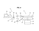
- FIG. 9 is a schematic view showing the polished-state inspection unit.
- This polished-state inspection unit is configured to determine whether or not a film (i.e., an object to be removed) has been removed from the periphery of the wafer by the polishing process based on an image taken by the imaging module.
- the polished-state inspection unit includes the above-mentioned imaging module 131 and an image processing section 132 for analyzing an image taken by the imaging module 131 .
- the imaging module 131 includes prisms 135 disposed so as to surround the periphery of the wafer W, an imaging camera 136 for taking an image of the periphery of the wafer W through the prisms 135 , and a focusing lens unit 137 disposed between the prisms 135 and the imaging camera 136 .
- a digital still camera having an image sensor e.g., CCD
- the imaging camera 136 and the image processing section 132 are coupled to each other, and the image, taken by the imaging camera 136 , is transmitted to the image processing section 132 .
- the wafer W is held by the above-described substrate holding rotary mechanism 61 .
- This substrate holding rotary mechanism 61 has a stepping motor 150 for rotating the wafer W about its own axis via the upper chuck 62 and the lower chuck 63 , and a rotary encoder (i.e., a position detector) 151 for detecting a rotational position or a rotational angle of the wafer W.
- a rotary encoder i.e., a position detector
- an absolute rotary encoder that detects an absolute position of the wafer W is used as the rotary encoder 151 .
- the imaging module 131 is movable by a non-illustrated drive mechanism toward and away from the wafer W held by the substrate holding rotary mechanism 61 .
- the focusing lens unit 137 includes a lens 140 arranged on an optical axis and an actuator (e.g., a linear motor) 141 for a focusing operation.
- the actuator 141 is configured to move the lens 140 along the optical axis.
- the image processing section 132 and the actuator 141 are electrically connected. Based on a command from the image processing section 132 , the actuator 141 moves the lens 140 such that the image is formed on the image sensor of the imaging camera 136 .
- a general-purpose personal computer can be used as the image processing section 132 .
- a half mirror 142 is provided between the prisms 135 and the lens 140 .
- Light is applied to the half mirror 142 from a light source (e.g., a white LED) 144 .
- a lens 145 is disposed between the light source 144 and the half mirror 142 . This lens 145 is provided for directing the light from the light source 144 to the periphery of the wafer W.
- the light from the light source 144 passes through the lens 145 and is reflected off the half mirror 142 to reach the periphery of the wafer W, whereby the periphery of the wafer W is brilliantly illuminated.
- the prisms 135 are arranged so as to face the upper portion and the lower portion of the periphery of the wafer W.
- Each of the prisms 135 has a property of adjusting an optical path length (or changing an optical path length). With use of the prisms 135 , the respective images of the upper portion, the middle portion, and the lower portion of the periphery of the wafer W can be formed on the image sensor simultaneously. “Chrovit” distributed by Chrovit Japan Inc. or TECHNICAL Inc. can be suitably used as the prisms 135 having such a property.
- FIG. 10 is a schematic view illustrating optical paths of the images.
- a plane A represents a surface of the image sensor of the imaging camera 136
- a plane B represents a plane that passes through a center of the lens 140
- a plane C represents the side portion (i.e., the apex) of the bevel portion of the wafer W
- planes D represent the upper slope and the lower slope of the bevel portion.
- the planes A, B, and C are parallel to each other.
- the plane A and the plane C are in a conjugate relationship by the lens 140 . Specifically, an image on the plane C forms an image on the plane A.
- Images on the planes D are once reflected in the prisms 135 and directed to the lens 140 .
- An optical path length d 1 from the plane C to the plane A and optical path lengths d 2 , d 3 from the plane D to the plane A through the prisms 135 are equal optically. This is because the optical path lengths d 2 , d 3 are adjusted (shortened) by the prisms 135 .
- the prisms 135 that are designed to equalize the optical path length d 1 and the optical path lengths d 2 , d 3 to each other are used in this embodiment.
- the image of the plane C and the images of the planes D are formed on the plane A (i.e., on the surface of the image sensor) by the lens 140 .
- An angle of the plane D is an angle of the bevel portion of the wafer and can vary depending on the type of wafer or the polished state (i.e., a degree of the polishing process). Consequently, the plane D and the plane A are not always parallel when the images are formed on the plane A, and the plane D in its entirety may not be focused on the plane A. In such a case, by increasing depth of focus of an optical system disposed between the plane D and the plane A, the image of the plane D can be formed on the plane A.
- One example of such a means for changing the depth of focus is to provide a diaphragm adjacent to the lens 140 . Specifically, in FIG. 10 , the diaphragm is disposed on the left side of the lens 140 . The depth of the focus can be increased by reducing an aperture of the diaphragm.
- the respective images of the upper portion, the middle portion, and the lower portion of the periphery of the wafer W are taken as images developed on the plane.
- the images of the upper portion and the lower portion of the periphery of the wafer W are taken by the imaging camera 136 through the prisms 135 .
- the image of the middle portion of the periphery of the wafer W is taken by the imaging camera 136 directly without the prisms 135 .
- the optical path length between the upper and lower portions of the periphery and the imaging camera 136 is equalized to the optical path length between the middle portion of the periphery and the imaging camera 136 by the prisms 135 .
- the imaging camera 136 can take the images of the peripheral portion of the wafer W from multiple directions simultaneously. In order to take better images, it is preferable to use the lens 140 of magnification such that the images are formed on the image sensor substantially in its entirety of the imaging camera 136 .
- the image-taking methods include a step-and-repeat method and a scan method.
- the step-and-repeat method is a method of taking still images of the periphery of the wafer W while rotating the wafer W intermittently
- the scan method is a method of taking accumulated images of the periphery of the wafer W while rotating the wafer W continuously.
- FIG. 11 is a view showing an example of image-pickup positions of the wafer in the step-and-repeat method
- FIG. 12 is a flowchart showing operation sequence of the step-and-repeat method. As shown in FIG. 11 , in this method, plural image-pickup positions on the periphery of the wafer W are predetermined.
- the image processing section 132 sends a command signal to the stepping motor 150 , so that the stepping motor 150 rotates the wafer W (step 1 ).
- the rotational position of the wafer W is measured by the rotary encoder 151 (step 2 ).
- the imaging camera 136 takes an image of the periphery of the wafer W (step 3 ).
- the captured image is transmitted to the image processing section 132 and stored in a memory (i.e., a storage device) of the image processing section 132 (step 4 ).
- the image processing section 132 processes the image according to an image processing method, which will be described later, to inspect the presence or absence of a residual film (step 5 ).
- the inspection result is stored in the memory of the image processing section 132 (step 6 ).
- Each image-pickup position is recorded (or registered) in the image processing section 132 in association with the rotational position or the rotational angle of the wafer W.
- the information indicating the position where the image was taken is transmitted from the rotary encoder 151 to the image processing section 132 , and this positional information is stored in the memory together with the corresponding image. Therefore, information of the residual film, such as a position and a size (an area) thereof, can be obtained from the image taken by the camera 136 .
- the information including the presence or absence of the residual film and the position of the residual film are stored as the inspection result in the memory.
- the above-described steps from the rotation of the wafer W (step 1 ) to the storage of the inspection result (step 6 ) are repeated until the inspection is conducted at all of the image-pickup positions.
- the image-pickup positions may be set only in part of the periphery of the wafer W, or may be set over the entire circumference of the wafer W. From the viewpoint of reliability of the inspection result, it is preferable to set the image-pickup positions over the entire circumference of the wafer W.
- FIGS. 13A and 13B are views each showing an example of image-pickup positions of the wafer in the scan method
- FIG. 14 is a flowchart showing operation sequence of the scan method.
- images of the periphery of the wafer W over its entire circumference are taken.
- the image processing section 132 sends a command signal to the stepping motor 150 , so that the stepping motor 150 rotates the wafer W (step 1 ).
- the rotational position of the wafer W is measured by the rotary encoder 151 (step 2 ).
- the imaging camera 136 starts taking the image of the periphery of the wafer W (step 3 ). While the wafer W is being rotated, the image sensor of the imaging camera 136 is exposed continuously.
- the imaging module 131 stops taking the image and moves away from the wafer W temporarily. After the craw 62 a of the upper chuck 62 has passed the prisms 135 , the imaging module 131 moves closer to the wafer W and starts taking the image of the periphery of the wafer W again.
- Such operations of taking the image and moving away from and toward the wafer W are repeated until the wafer W makes one revolution.
- the images, taken by the imaging camera 136 are sent to the image processing section 132 and stored in the memory of the image processing section 132 .
- the upper chuck 62 has four claws 62 a . Therefore, the imaging camera 136 repeats taking the image four times to thereby obtain images of four regions F 1 , F 2 , F 3 , and F 4 .
- the rotation of the wafer W is stopped and the imaging module 131 is moved to its idle position once.
- the lower chuck 63 is elevated to hold the wafer W, whereby the wafer W is transferred from the upper chuck 62 to the lower chuck 63 .
- the upper chuck 62 is rotated through 45 degrees and then the lower chuck 63 is lowered, whereby the wafer W is held by the upper chuck 62 at a different position (step 4 ).
- the imaging module 131 moves toward the wafer W and starts taking the image at the same time as the wafer W is rotated.
- the imaging module 131 repeats the operations of taking the images and moving away from the wafer in the same manner as described above until the wafer W makes one revolution (step 5 ). More specifically, as shown in FIG. 13B , the imaging camera 136 repeats taking the image four times to thereby obtain images of four regions F 5 , F 6 , F 7 , and F 8 which overlap the above-mentioned regions F 1 , F 2 , F 3 , and F 4 . In this manner, the images of the periphery of the wafer W in its entirety are obtained. The images obtained are transmitted to the image processing section 132 and stored in the memory of the image processing section 132 .
- the image processing section 132 processes the image according to the image processing method which will be described later, and inspects whether or not the film remains on the periphery of the wafer W (step 6 ).
- the inspection result is stored in the memory of the image processing section 132 (step 7 ).
- a line scan camera may be used as the imaging camera 136 .
- the line scan camera is a camera configured to capture linear images successively and arrange the captured images sequentially to create a wide image (or a horizontally-long image).
- the information indicating a position where each image was taken is transmitted from the rotary encoder 151 to the image processing section 132 , and this positional information is stored in the memory together with the corresponding image.
- Use of the line scan camera makes it possible to specify an accurate position and a size of the residual film.
- the step-and-repeat method and the scan method may be used in combination.
- high-speed inspection can be performed by the scan method and then more precise inspection can be performed by the step-and-repeat method.
- the above-described step-and-repeat method is used, or a combination of the scan method and the line scan camera is used.
- the image processing section 132 has an image display device which can display the images saved in the memory.
- the image display device may be provided independently of the image processing section 132 .
- each image is stored in the memory in association with the rotational position or rotational angle of the wafer W that indicates the position of the image. Therefore, an image in a desired position can be displayed on the image display device.
- the image processing section 132 judges that the film still remains at a certain position, the image processing section 132 can command the imaging module 131 to take an image at the same position again and can display the captured image on the image display device.
- the above-described polishing unit is used to perform five-stage polishing on five areas A 1 , A 2 , A 3 , A 4 , and A 5 which are separately defined in the bevel portion of the wafer W, as shown in FIG. 15 .
- the bevel polishing head 85 is inclined in a manner as shown in FIG. 8A through FIG. 8C to polish the areas A 1 , A 2 , A 3 , A 4 , and A 5 successively.
- the bevel portion is polished in this example, the near-edge portions can also be polished as well.
- the polished wafer W is cleaned by the primary cleaning unit 100 and further cleaned and dried by the secondary cleaning-drying unit 110 .
- the dried wafer W is transported to the measuring unit 30 , where the images of the periphery of the wafer W are captured by the imaging module 131 as described previously.
- FIG. 16 is a schematic view illustrating images of the periphery of the wafer taken by the imaging module.
- Reference numeral 200 A represents an image of the periphery of the wafer captured through the upper prism 135
- reference numeral 200 B represents an image of the periphery of the wafer captured directly without the prisms 135
- reference numeral 200 C represents an image of the periphery of the wafer captured through the lower prism 135 .
- images of the areas A 1 and A 2 located in the upper portion of the bevel portion are captured by the imaging camera 136 through the upper prism 135
- an image of the area A 3 located in the middle portion of the bevel portion is captured by the imaging camera 136 directly with no prism intervening between the wafer W and the camera 136
- images of the areas A 4 and A 5 located in the lower portion of the bevel portion are captured by the imaging camera 136 through the lower prism 135 .
- the imaging camera 136 can take the three images 200 A, 200 B, and 200 C simultaneously in one field of view, and an adjustment of focus can also be performed simultaneously.
- Specific regions to be monitored by the image processing section 132 are set in the areas A 1 , A 2 , A 3 , A 4 , and A 5 , respectively.
- these specific regions will be referred to as target regions T 1 , T 2 , T 3 , T 4 , and T 5 .
- the image processing section 132 monitors colors of these target regions T 1 , T 2 , T 3 , T 4 , and T 5 and determines whether or not the film has been removed based on change in the colors.
- the target regions T 1 , T 2 , T 3 , T 4 , and T 5 to be selected are regions which most suitably represent the polished-state of the areas A 1 , A 2 , A 3 , A 4 , and A 5 .
- Plural target regions may be set in one area.
- the image processing section 132 determines removal of the film based on the color of the target region.
- a predetermined target color is registered in advance in the image processing section 132 .
- the image processing section 132 determines that the film has been removed when the color of the target region matches the preset target color. More specifically, the image processing section 132 determines that the film has been removed when the number of pixels of the target color in the target region is larger than a predetermined threshold or smaller than a predetermined threshold.
- the target color can be selected from either a color of an exposed surface that appears as a result of polishing of the wafer (e.g., a color of silicon) or a color of an object to be removed (e.g., a color of SiO 2 or SiN).
- the color to be selected is not limited to a single color, and multiple colors can be selected.
- FIG. 17 is a view showing a color chart and a brightness chart for use in setting of the target color. As shown in FIG. 17 , the color chart has a horizontal axis representing hue and a vertical axis representing saturation.
- the brightness chart has a vertical axis representing a degree of brightness.
- the target color can be determined from color information (hue, saturation, brightness) specified by a scope S 1 located in the color chart and a scope S 2 located in the brightness chart.
- the color of silicon (typically white) is registered as the target color in the image processing section 132 (step 1 ).
- the color to be selected is not limited to a single color, and multiple colors can be selected.
- the target region is specified (step 2 ). Then, if the number N of pixels of the target color in the target region is larger than a predetermined threshold P, the image processing section 132 determines that the film has been removed by the polishing process. This is because, when the film is removed by the polishing process, the color of the underlying silicon appears on the exposed surface. On the other hand, if the number N of pixels of the target color in the target region is equal to or smaller than the predetermined threshold P, the image processing section 132 determines that the film remains on the wafer W (step 3 ).
- FIG. 19 is a diagram showing a film-removal determining process in a case where the color of the film to be removed is selected as the target color.
- the color of the film to be removed is registered as the target color in the image processing section 132 (step 1 ).
- the color to be selected is not limited to a single color, and multiple colors can be selected.
- the target region is specified (step 2 ).
- the image processing section 132 determines that the film has been removed by the polishing process. This is because, when the film is removed by the polishing process, the color of the film disappears.
- the image processing section 132 determines that the film remains on the wafer W (step 3 ).
- the inspection results are transmitted to the polishing-condition determining section 120 and used for determining the polishing conditions. For example, in the case where the image processing section 132 has determined that the film remains on the wafer, this inspection results is reflected on the polishing conditions (e.g., a polishing time and a force of pressing the polishing tape) for a subsequent wafer. Because the inspection results are obtained for the five areas A 1 , A 2 , A 3 , A 4 , and A 5 , the polishing conditions can be changed for these five areas in accordance with the inspection results. It is preferable to return the wafer, still having the residual film, to the polishing unit 70 A or 70 B and polish it again. In this case, the polishing time can be set to be shorter than the polishing time of the first polishing process.
- the polishing time can be set to be shorter than the polishing time of the first polishing process.
- the above-described example is directed to the method of inspecting the polished-state (i.e., the polished surface) based on the change in color of the image captured.
- a surface roughness of the periphery of the wafer can be detected from the image captured.
- a method of detecting the surface roughness of the periphery of the wafer will be described.
- the surface-roughness detecting method it is preferable to use the above-described step-and-repeat method or a combination of the scan method and the line scan camera.
- the image, taken by the imaging camera 136 , is sent to the image processing section 132 , where image processing is performed. Specifically, the target region (T 1 to T 5 ) is extracted from the image, and the extracted color image is converted into a black-and-white image. Next, in order to emphasize the surface roughness, the black-and-white image is subjected to differential processing by applying a differentiation filter. Then the resultant image is displayed on a histogram. This histogram has a horizontal axis representing a brightness and a vertical axis representing the number of pixels.
- FIG. 20A is a schematic view showing an image of the periphery of the wafer with a rough surface and showing the image that has been subjected to the differential processing.
- FIG. 20B is a histogram that numerically expresses the image shown in FIG. 20A .
- the surface roughness can be expressed as a numerical value on the histogram. Specifically, when the polished surface is rough, a lot of white areas appear in the image. As a result, the number of pixels of high brightness increases on the histogram.
- FIG. 21A is a schematic view showing an image of the periphery of the wafer with a smooth surface and showing the image that has been subjected to the differential processing.
- FIG. 21B is a histogram that numerically expresses the image shown in FIG. 21A .
- FIG. 21A when the polished surface of the wafer W is smooth, white areas indicating surface irregularities hardly appear on the image. As a result, the number of pixels of low brightness increases on the histogram.
- the image processing section 132 can determines that the surface of the periphery of the wafer W is smooth when the number of pixels of predetermined brightness is larger than a preset value (e.g., when the number of pixels of brightness in the range of 0 to 64 is larger than 1000), or smaller than a preset value (e.g., when the number of pixels of brightness of 64 or more is smaller than 10).
- a preset value e.g., when the number of pixels of brightness in the range of 0 to 64 is larger than 1000
- a preset value e.g., when the number of pixels of brightness of 64 or more is smaller than 10
- the imaging module 131 includes plural terminal image-pickup elements (e.g., objective lenses) 160 A, 160 B, and 160 C and imaging cameras 136 A, 136 B, and 136 C coupled to the terminal image-pickup elements 160 A, 160 B, and 160 C, respectively, via optical fibers.
- plural terminal image-pickup elements e.g., objective lenses
- imaging cameras 136 A, 136 B, and 136 C coupled to the terminal image-pickup elements 160 A, 160 B, and 160 C, respectively, via optical fibers.
- the terminal image-pickup element 160 A is located above the wafer W, the terminal image-pickup element 160 B is located laterally of the wafer W, and the terminal image-pickup element 160 C is located below the wafer W
- Illuminators 163 A, 163 B, 163 C, and 163 D are disposed next to the terminal image-pickup elements 160 A, 160 B, and 160 C.
- the terminal image-pickup elements 160 A to 160 C and the illuminators 163 A to 163 D are secured to a support member 165 .
- the imaging cameras 136 A, 136 B, and 136 C are coupled to the image processing section 132 .
- All the terminal image-pickup elements 160 A to 160 C and the illuminators 163 A to 163 D are arranged so as to face the periphery of the wafer W. More specifically, the terminal image-pickup element 160 A faces the upper portion of the periphery of the wafer W, the terminal image-pickup element 160 B faces the middle portion of the periphery of the wafer W, and the terminal image-pickup element 160 C faces the lower portion of the periphery of the wafer W.
- the images of the upper portion, the middle portion, and the lower portion of the periphery of the wafer W are taken by the imaging cameras 136 A to 136 C through the terminal image-pickup elements 160 A to 160 C.
- the images captured are transmitted to the image processing section 132 and are processed in accordance with the above-described method.
- FIG. 23A is a schematic view showing another modified example of the imaging module.
- a second imaging module 170 for taking an image of the rear surface of the wafer W is provided.
- This second imaging module 170 has a mirror 171 , instead of the above-described prisms 135 .
- the second imaging module 170 has a wider field of view (image-pickup coverage) than that of the first imaging module 131 .
- Other structures are identical to those of the first imaging module 131 .
- the mirror 171 is movable together with an imaging camera (see FIG. 9 ) of the second imaging module 170 in unison.
- the image of the rear surface of the wafer W is reflected off the mirror 171 to change its direction, and captured by the second imaging module 170 .
- the wafer W is held by the substrate holding rotary mechanism 61 .
- FIG. 23B is a schematic view showing a region to be photographed by the second imaging module 170 .
- the region to be photographed by the second imaging module 170 is a flat surface located radially inwardly of the bevel portion and including the back near-edge portion. A width of the region is about 6 mm.
- the second imaging module 170 moves in conjunction with the first imaging module 131 and takes the image at the same timing.
- the image captured by the second imaging module 170 is transmitted to the image processing section 132 and are processed in accordance with the above-described method.
- the imaging module 131 is incorporated in the measuring unit 30 in the above-described embodiment, the present invention is not limited to this arrangement.
- the imaging module 131 and the substrate holding rotary mechanism 61 may be provided as one unit independently of other units.
- the substrate holding rotary mechanism may be of attraction type that holds the rear surface of the wafer by an attraction force (e.g., a vacuum suction).
- the measuring unit to be incorporated in the substrate processing apparatus include a measuring unit for measuring other physical quantity, such as a shape or temperature of the wafer.
- the above-described imaging module 131 can be provided in such a measuring unit which measures a predetermined physical quantity of the wafer in a dry state. Further, the above-described imaging module 131 can also be provided in a post-processing unit for performing a post-process, such as a drying process, on the wafer.
- the imaging module 131 may be incorporated in the secondary cleaning-drying unit 110 , so that the polished state can be inspected after drying of the wafer W. Further, plural imaging cameras and plural terminal image-pickup elements may be provided separately in plural units (e.g., in the measuring unit 30 and the secondary cleaning-drying unit 110 ).
- the imaging module 131 inspect the wafer W after the wafer W is cleaned and dried
- the present invention is not limited to this manner.
- the imaging module 131 may be provided in the first polishing unit 70 A and/or the second polishing unit 70 B.
- the imaging module 131 when the bevel polishing head 85 is polishing the wafer W, the imaging module 131 is in a location away from the wafer W, and when the bevel polishing head 85 moves away from the wafer W, the imaging module 131 moves toward the wafer W and takes the image of the periphery of the wafer W. According to these operations, even if the multiple bevel polishing heads 85 are provided around the wafer W, the bevel polishing heads 85 and the imaging module 131 do not contact and the respective processes do not interfere with each other.
- the imaging module 131 of in-line type is configured to take the image of the wafer W when the polishing process is not being performed. For example, after polishing of the wafer W is completed, the imaging module 131 provided inside or outside the polishing unit may take the image of the periphery of the wafer W. Alternatively, the imaging module 131 provided in the polishing unit may take the image of the periphery of the wafer W when polishing of the wafer W is stopped temporarily, and after taking the image, polishing of the wafer W may be performed again.
Landscapes
- Engineering & Computer Science (AREA)
- Mechanical Engineering (AREA)
- Chemical & Material Sciences (AREA)
- Ceramic Engineering (AREA)
- Inorganic Chemistry (AREA)
- Constituent Portions Of Griding Lathes, Driving, Sensing And Control (AREA)
- Mechanical Treatment Of Semiconductor (AREA)
- Testing Or Measuring Of Semiconductors Or The Like (AREA)
Applications Claiming Priority (2)
| Application Number | Priority Date | Filing Date | Title |
|---|---|---|---|
| JP2008191882A JP5160993B2 (ja) | 2008-07-25 | 2008-07-25 | 基板処理装置 |
| JP2008-191882 | 2008-07-25 |
Publications (2)
| Publication Number | Publication Date |
|---|---|
| US20100022166A1 US20100022166A1 (en) | 2010-01-28 |
| US8414355B2 true US8414355B2 (en) | 2013-04-09 |
Family
ID=41569066
Family Applications (1)
| Application Number | Title | Priority Date | Filing Date |
|---|---|---|---|
| US12/458,814 Active 2032-01-11 US8414355B2 (en) | 2008-07-25 | 2009-07-23 | Substrate processing apparatus |
Country Status (2)
| Country | Link |
|---|---|
| US (1) | US8414355B2 (enExample) |
| JP (1) | JP5160993B2 (enExample) |
Cited By (1)
| Publication number | Priority date | Publication date | Assignee | Title |
|---|---|---|---|---|
| US20180277401A1 (en) * | 2017-03-27 | 2018-09-27 | Ebara Corporation | Substrate processing method and apparatus |
Families Citing this family (21)
| Publication number | Priority date | Publication date | Assignee | Title |
|---|---|---|---|---|
| JP5254575B2 (ja) * | 2007-07-11 | 2013-08-07 | 株式会社東芝 | 研磨装置および研磨方法 |
| KR101236472B1 (ko) * | 2007-10-15 | 2013-02-22 | 삼성전자주식회사 | 웨이퍼 베벨 영역 폴리싱 장치 및 그 장치에서의 연마종말점 검출 방법 |
| JP5393039B2 (ja) | 2008-03-06 | 2014-01-22 | 株式会社荏原製作所 | 研磨装置 |
| US20100105290A1 (en) * | 2008-10-24 | 2010-04-29 | Applied Materials, Inc. | Methods and apparatus for indicating a polishing tape end |
| FR2975940A1 (fr) * | 2011-05-31 | 2012-12-07 | Forest Line Capdenac | Procede de controle du jeu entre bandes deposees par une tete de drapage et sous-ensemble de tete de drapage a dispositif de controle embarque. |
| JP5976331B2 (ja) * | 2012-02-03 | 2016-08-23 | 株式会社ディスコ | 研削装置 |
| JP6140439B2 (ja) * | 2012-12-27 | 2017-05-31 | 株式会社荏原製作所 | 研磨装置、及び研磨方法 |
| JP6100002B2 (ja) * | 2013-02-01 | 2017-03-22 | 株式会社荏原製作所 | 基板裏面の研磨方法および基板処理装置 |
| JP6071611B2 (ja) * | 2013-02-13 | 2017-02-01 | Mipox株式会社 | オリエンテーションフラット等切り欠き部を有する、結晶材料から成るウエハの周縁を、研磨テープを使用して研磨することにより円形ウエハを製造する方法 |
| JP2014200888A (ja) * | 2013-04-05 | 2014-10-27 | ローム株式会社 | 吸引保持装置およびウエハ研磨装置 |
| JP6327329B1 (ja) * | 2016-12-20 | 2018-05-23 | 株式会社Sumco | シリコンウェーハの研磨方法およびシリコンウェーハの製造方法 |
| KR101868786B1 (ko) * | 2017-08-08 | 2018-06-19 | 김인수 | 휴대기기 글라스 성형용 금형의 제조장치 |
| JP7029914B2 (ja) * | 2017-09-25 | 2022-03-04 | 東京エレクトロン株式会社 | 基板処理装置 |
| JP6713015B2 (ja) * | 2018-04-13 | 2020-06-24 | 株式会社大気社 | 自動研磨システム |
| CN109604116B (zh) * | 2018-11-29 | 2021-04-09 | 安徽荣泽科技有限公司 | 一种全自动特种胶带涂布机 |
| JP7282461B2 (ja) * | 2019-04-16 | 2023-05-29 | 株式会社ディスコ | 検査装置、及び加工装置 |
| JP7350544B2 (ja) * | 2019-07-11 | 2023-09-26 | 株式会社荏原製作所 | 研磨装置および研磨方法 |
| CN111300161B (zh) * | 2020-02-26 | 2022-02-01 | 上海东竞自动化系统有限公司 | 表面划痕修复的方法和设备 |
| JP2024158608A (ja) * | 2023-04-28 | 2024-11-08 | 株式会社Screenホールディングス | 撮像装置、基板観察装置、基板処理装置および撮像方法 |
| JP2025083039A (ja) * | 2023-11-20 | 2025-05-30 | 株式会社荏原製作所 | 基板処理装置および基板処理方法 |
| TWI898454B (zh) * | 2024-02-29 | 2025-09-21 | 東台精機股份有限公司 | 晶圓研磨裝置及晶圓研磨方法 |
Citations (29)
| Publication number | Priority date | Publication date | Assignee | Title |
|---|---|---|---|---|
| US4319270A (en) * | 1979-01-12 | 1982-03-09 | Kobe Steel, Ltd. | Surface inspection system for hot radiant material |
| JPH07276229A (ja) | 1994-04-01 | 1995-10-24 | Nippon Steel Corp | 半導体ウエハエッジ部研磨装置 |
| US5604583A (en) * | 1995-03-20 | 1997-02-18 | Bausch & Lomb Incorporated | Computer vision inspection station |
| US5613894A (en) * | 1993-12-30 | 1997-03-25 | Delle Vedove Levigatrici Spa | Method to hone curved and shaped profiles and honing machine to carry out such method |
| US5738563A (en) * | 1995-03-07 | 1998-04-14 | Kao Corporation | Substrate chamfering machine |
| JPH11351850A (ja) | 1998-06-04 | 1999-12-24 | Sumitomo Osaka Cement Co Ltd | 端部傷検査方法およびその装置 |
| JP2999712B2 (ja) | 1996-03-29 | 2000-01-17 | 住友金属工業株式会社 | 端部欠陥検査方法とその装置 |
| JP2000114329A (ja) | 1998-09-29 | 2000-04-21 | Yuhi Denshi Kk | 基板端部の研削面の検査方法とその装置 |
| US6122063A (en) * | 1997-04-10 | 2000-09-19 | Fraunhofer-Gesellschaft Zur Forderung Der Angewandten Forschung E.V. | Measuring device and method for contactless determining of the 3-dimensional form of a peripheral groove in a spectacle frame |
| US6174222B1 (en) * | 1995-06-09 | 2001-01-16 | Hitachi, Ltd. | Process for fabrication of semiconductor device, semiconductor wafer for use in the process and process for the preparation of the wafer |
| US20010000502A1 (en) * | 1996-06-15 | 2001-04-26 | Stocker Mark Andrew | Grinding and polishing machines |
| JP2002208572A (ja) | 2001-01-09 | 2002-07-26 | Ebara Corp | 研磨装置 |
| US20030169916A1 (en) | 2002-02-19 | 2003-09-11 | Toshiba Ceramics Co., Ltd. | Wafer inspection apparatus |
| US20030190862A1 (en) * | 2002-03-21 | 2003-10-09 | Kyung-Su Chae | Apparatus and method for correcting grinding amount of liquid crystal display panel |
| US6749377B2 (en) * | 2001-04-20 | 2004-06-15 | Loh Optikmaschinen Ag | Process for edge-machining of optical lenses |
| US6813536B1 (en) * | 1998-02-05 | 2004-11-02 | Wernicke & Co. Gmbh | Method and device for computer numerical control of machining of spectacle lenses |
| US6840841B2 (en) | 2002-01-15 | 2005-01-11 | Speedfam Co., Ltd. | Wafer edge polishing system |
| US20050018280A1 (en) * | 1998-07-10 | 2005-01-27 | Richardson Timothy M. | Braced microscope |
| US6881130B1 (en) * | 1999-07-03 | 2005-04-19 | Unova U.K. Limited | Edge grinding |
| JP2005191179A (ja) | 2003-12-25 | 2005-07-14 | Trecenti Technologies Inc | 半導体装置の製造方法および研磨装置 |
| US6933234B2 (en) | 2001-11-26 | 2005-08-23 | Kabushiki Kaisha Toshiba | Method for manufacturing semiconductor device and polishing apparatus |
| WO2005081301A1 (en) | 2004-02-25 | 2005-09-01 | Ebara Corporation | Polishing apparatus and substrate processing apparatus |
| US7004821B2 (en) * | 2002-04-12 | 2006-02-28 | Essilor International (Compagnie Generale D'optique) | Process for bevelling an ohthalmic lens including a plotting stage without contact |
| US7066787B2 (en) | 2003-02-03 | 2006-06-27 | Ebara Corporation | Substrate processing apparatus |
| WO2006112530A1 (en) | 2005-04-19 | 2006-10-26 | Ebara Corporation | Substrate processing apparatus |
| JP2007155448A (ja) | 2005-12-02 | 2007-06-21 | Olympus Corp | 端面検査装置 |
| US20080274670A1 (en) | 2004-05-28 | 2008-11-06 | Ebara Corporation | Substrate Peripheral Portion Measuring Device, and Substrate Peripheral Portion Polishing Apparatus |
| US7528922B2 (en) * | 2002-12-17 | 2009-05-05 | Lg Display Co., Ltd. | Apparatus and method for measuring ground amounts of liquid crystal display panel |
| JP2009111079A (ja) | 2007-10-29 | 2009-05-21 | Toshiba Corp | 基板の周縁部の処理方法および装置 |
Family Cites Families (2)
| Publication number | Priority date | Publication date | Assignee | Title |
|---|---|---|---|---|
| JP2005217139A (ja) * | 2004-01-29 | 2005-08-11 | Dainippon Screen Mfg Co Ltd | 画像取得装置および画像取得方法 |
| JP4626982B2 (ja) * | 2005-02-10 | 2011-02-09 | セントラル硝子株式会社 | ガラス板の端面の欠陥検出装置および検出方法 |
-
2008
- 2008-07-25 JP JP2008191882A patent/JP5160993B2/ja active Active
-
2009
- 2009-07-23 US US12/458,814 patent/US8414355B2/en active Active
Patent Citations (32)
| Publication number | Priority date | Publication date | Assignee | Title |
|---|---|---|---|---|
| US4319270A (en) * | 1979-01-12 | 1982-03-09 | Kobe Steel, Ltd. | Surface inspection system for hot radiant material |
| US5613894A (en) * | 1993-12-30 | 1997-03-25 | Delle Vedove Levigatrici Spa | Method to hone curved and shaped profiles and honing machine to carry out such method |
| JPH07276229A (ja) | 1994-04-01 | 1995-10-24 | Nippon Steel Corp | 半導体ウエハエッジ部研磨装置 |
| US5738563A (en) * | 1995-03-07 | 1998-04-14 | Kao Corporation | Substrate chamfering machine |
| US5604583A (en) * | 1995-03-20 | 1997-02-18 | Bausch & Lomb Incorporated | Computer vision inspection station |
| US6174222B1 (en) * | 1995-06-09 | 2001-01-16 | Hitachi, Ltd. | Process for fabrication of semiconductor device, semiconductor wafer for use in the process and process for the preparation of the wafer |
| JP2999712B2 (ja) | 1996-03-29 | 2000-01-17 | 住友金属工業株式会社 | 端部欠陥検査方法とその装置 |
| US20010000502A1 (en) * | 1996-06-15 | 2001-04-26 | Stocker Mark Andrew | Grinding and polishing machines |
| US6122063A (en) * | 1997-04-10 | 2000-09-19 | Fraunhofer-Gesellschaft Zur Forderung Der Angewandten Forschung E.V. | Measuring device and method for contactless determining of the 3-dimensional form of a peripheral groove in a spectacle frame |
| US6813536B1 (en) * | 1998-02-05 | 2004-11-02 | Wernicke & Co. Gmbh | Method and device for computer numerical control of machining of spectacle lenses |
| JPH11351850A (ja) | 1998-06-04 | 1999-12-24 | Sumitomo Osaka Cement Co Ltd | 端部傷検査方法およびその装置 |
| US20050018280A1 (en) * | 1998-07-10 | 2005-01-27 | Richardson Timothy M. | Braced microscope |
| JP2000114329A (ja) | 1998-09-29 | 2000-04-21 | Yuhi Denshi Kk | 基板端部の研削面の検査方法とその装置 |
| US6881130B1 (en) * | 1999-07-03 | 2005-04-19 | Unova U.K. Limited | Edge grinding |
| JP2002208572A (ja) | 2001-01-09 | 2002-07-26 | Ebara Corp | 研磨装置 |
| US6749377B2 (en) * | 2001-04-20 | 2004-06-15 | Loh Optikmaschinen Ag | Process for edge-machining of optical lenses |
| US6933234B2 (en) | 2001-11-26 | 2005-08-23 | Kabushiki Kaisha Toshiba | Method for manufacturing semiconductor device and polishing apparatus |
| US6840841B2 (en) | 2002-01-15 | 2005-01-11 | Speedfam Co., Ltd. | Wafer edge polishing system |
| US20030169916A1 (en) | 2002-02-19 | 2003-09-11 | Toshiba Ceramics Co., Ltd. | Wafer inspection apparatus |
| US20030190862A1 (en) * | 2002-03-21 | 2003-10-09 | Kyung-Su Chae | Apparatus and method for correcting grinding amount of liquid crystal display panel |
| US7497762B2 (en) * | 2002-03-21 | 2009-03-03 | Lg Display Co., Ltd. | Apparatus and method for correcting grinding amount of liquid crystal display panel |
| US7004821B2 (en) * | 2002-04-12 | 2006-02-28 | Essilor International (Compagnie Generale D'optique) | Process for bevelling an ohthalmic lens including a plotting stage without contact |
| US7528922B2 (en) * | 2002-12-17 | 2009-05-05 | Lg Display Co., Ltd. | Apparatus and method for measuring ground amounts of liquid crystal display panel |
| US7066787B2 (en) | 2003-02-03 | 2006-06-27 | Ebara Corporation | Substrate processing apparatus |
| JP2005191179A (ja) | 2003-12-25 | 2005-07-14 | Trecenti Technologies Inc | 半導体装置の製造方法および研磨装置 |
| WO2005081301A1 (en) | 2004-02-25 | 2005-09-01 | Ebara Corporation | Polishing apparatus and substrate processing apparatus |
| US20090117828A1 (en) * | 2004-02-25 | 2009-05-07 | Akihisa Hongo | Polishing apparatus and substrate processing apparatus |
| US20080274670A1 (en) | 2004-05-28 | 2008-11-06 | Ebara Corporation | Substrate Peripheral Portion Measuring Device, and Substrate Peripheral Portion Polishing Apparatus |
| US20080200100A1 (en) | 2005-04-19 | 2008-08-21 | Ebara Corporation | Substrate Processing Apparatus |
| WO2006112530A1 (en) | 2005-04-19 | 2006-10-26 | Ebara Corporation | Substrate processing apparatus |
| JP2007155448A (ja) | 2005-12-02 | 2007-06-21 | Olympus Corp | 端面検査装置 |
| JP2009111079A (ja) | 2007-10-29 | 2009-05-21 | Toshiba Corp | 基板の周縁部の処理方法および装置 |
Non-Patent Citations (2)
| Title |
|---|
| Machine English translation of JP 2002-208572. |
| Machine English translation of JP 2007-155448. |
Cited By (2)
| Publication number | Priority date | Publication date | Assignee | Title |
|---|---|---|---|---|
| US20180277401A1 (en) * | 2017-03-27 | 2018-09-27 | Ebara Corporation | Substrate processing method and apparatus |
| US10811284B2 (en) * | 2017-03-27 | 2020-10-20 | Ebara Corporation | Substrate processing method and apparatus |
Also Published As
| Publication number | Publication date |
|---|---|
| JP5160993B2 (ja) | 2013-03-13 |
| JP2010034118A (ja) | 2010-02-12 |
| US20100022166A1 (en) | 2010-01-28 |
Similar Documents
| Publication | Publication Date | Title |
|---|---|---|
| US8414355B2 (en) | Substrate processing apparatus | |
| US9287158B2 (en) | Substrate processing apparatus | |
| KR101214507B1 (ko) | 기판 처리 장치, 기판 폴리싱 방법 및 기판 처리 방법 | |
| JP4772679B2 (ja) | 研磨装置及び基板処理装置 | |
| US5909276A (en) | Optical inspection module and method for detecting particles and defects on substrates in integrated process tools | |
| TW200303807A (en) | Polishing apparatus and method for detecting foreign matter on polishing surface | |
| US9570334B2 (en) | Method and system for positioning wafer in semiconductor manufacturing fabrication | |
| CN109427609B (zh) | 半导体晶片在线检验的系统及方法 | |
| US20130100441A1 (en) | Optical inspection apparatus and edge inspection device | |
| US20150017745A1 (en) | Polishing method and polishing apparatus | |
| KR20170113098A (ko) | 기판 처리 장치, 기판 처리 장치의 제어 방법, 및 기판 처리 시스템 | |
| JP6614978B2 (ja) | 研磨装置及び研磨方法 | |
| US8771038B2 (en) | Polishing apparatus | |
| KR102873657B1 (ko) | 기판 세정 시스템에서 두께를 모니터링하기 위한 이미징 | |
| CN115078402B (zh) | 一种用于检测硅片的系统 | |
| KR20070002257A (ko) | 웨이퍼 후면 결함 검출 장치 | |
| JP2001091474A (ja) | 欠陥検査システム | |
| JP2025030184A (ja) | 基板エッジ検出方法 | |
| WO2024252981A1 (ja) | 基板検査装置、基板検査方法及び記憶媒体 | |
| TW202518537A (zh) | 判斷具有用於在基板上形成平面化膜之平坦表面的壓迫構件之表面的裝置、平面化裝置及物品製造方法 |
Legal Events
| Date | Code | Title | Description |
|---|---|---|---|
| AS | Assignment |
Owner name: EBARA CORPORATION, JAPAN Free format text: ASSIGNMENT OF ASSIGNORS INTEREST;ASSIGNORS:KIMBA, TOSHIFUMI;KUSA, HIROAKI;REEL/FRAME:023031/0017 Effective date: 20090710 |
|
| STCF | Information on status: patent grant |
Free format text: PATENTED CASE |
|
| FPAY | Fee payment |
Year of fee payment: 4 |
|
| MAFP | Maintenance fee payment |
Free format text: PAYMENT OF MAINTENANCE FEE, 8TH YEAR, LARGE ENTITY (ORIGINAL EVENT CODE: M1552); ENTITY STATUS OF PATENT OWNER: LARGE ENTITY Year of fee payment: 8 |
|
| MAFP | Maintenance fee payment |
Free format text: PAYMENT OF MAINTENANCE FEE, 12TH YEAR, LARGE ENTITY (ORIGINAL EVENT CODE: M1553); ENTITY STATUS OF PATENT OWNER: LARGE ENTITY Year of fee payment: 12 |