US8324498B2 - Method of forming crystalline layer, and thin film solar cell and method of fabricating the solar cell adopting the method of forming crystalline layer - Google Patents
Method of forming crystalline layer, and thin film solar cell and method of fabricating the solar cell adopting the method of forming crystalline layer Download PDFInfo
- Publication number
- US8324498B2 US8324498B2 US12/270,588 US27058808A US8324498B2 US 8324498 B2 US8324498 B2 US 8324498B2 US 27058808 A US27058808 A US 27058808A US 8324498 B2 US8324498 B2 US 8324498B2
- Authority
- US
- United States
- Prior art keywords
- solar cell
- electrode
- support
- thin film
- photoelectric conversion
- Prior art date
- Legal status (The legal status is an assumption and is not a legal conclusion. Google has not performed a legal analysis and makes no representation as to the accuracy of the status listed.)
- Expired - Fee Related, expires
Links
- 239000010409 thin film Substances 0.000 title claims description 29
- 238000000034 method Methods 0.000 title abstract description 39
- 238000004519 manufacturing process Methods 0.000 title description 14
- 238000010438 heat treatment Methods 0.000 claims abstract description 120
- 239000000758 substrate Substances 0.000 claims abstract description 36
- 239000000463 material Substances 0.000 claims description 44
- 238000006243 chemical reaction Methods 0.000 claims description 26
- VYPSYNLAJGMNEJ-UHFFFAOYSA-N Silicium dioxide Chemical compound O=[Si]=O VYPSYNLAJGMNEJ-UHFFFAOYSA-N 0.000 claims description 8
- 229910052710 silicon Inorganic materials 0.000 claims description 8
- 229910052681 coesite Inorganic materials 0.000 claims description 4
- 150000001875 compounds Chemical class 0.000 claims description 4
- 229910052906 cristobalite Inorganic materials 0.000 claims description 4
- 239000000377 silicon dioxide Substances 0.000 claims description 4
- 229910052682 stishovite Inorganic materials 0.000 claims description 4
- 229910052905 tridymite Inorganic materials 0.000 claims description 4
- 229910052732 germanium Inorganic materials 0.000 claims description 3
- 239000004065 semiconductor Substances 0.000 description 75
- 229910021417 amorphous silicon Inorganic materials 0.000 description 14
- 238000002425 crystallisation Methods 0.000 description 10
- 230000008025 crystallization Effects 0.000 description 9
- 238000005229 chemical vapour deposition Methods 0.000 description 8
- XUIMIQQOPSSXEZ-UHFFFAOYSA-N Silicon Chemical compound [Si] XUIMIQQOPSSXEZ-UHFFFAOYSA-N 0.000 description 7
- 229910021420 polycrystalline silicon Inorganic materials 0.000 description 7
- 239000010703 silicon Substances 0.000 description 7
- 239000013078 crystal Substances 0.000 description 5
- 238000009826 distribution Methods 0.000 description 4
- 230000003287 optical effect Effects 0.000 description 4
- 238000010586 diagram Methods 0.000 description 3
- 238000005240 physical vapour deposition Methods 0.000 description 3
- 230000015556 catabolic process Effects 0.000 description 2
- 239000004020 conductor Substances 0.000 description 2
- 238000006731 degradation reaction Methods 0.000 description 2
- 238000000313 electron-beam-induced deposition Methods 0.000 description 2
- 238000005530 etching Methods 0.000 description 2
- GNPVGFCGXDBREM-UHFFFAOYSA-N germanium atom Chemical compound [Ge] GNPVGFCGXDBREM-UHFFFAOYSA-N 0.000 description 2
- 239000011521 glass Substances 0.000 description 2
- 230000035939 shock Effects 0.000 description 2
- 238000004544 sputter deposition Methods 0.000 description 2
- 238000003491 array Methods 0.000 description 1
- 238000004581 coalescence Methods 0.000 description 1
- 238000010960 commercial process Methods 0.000 description 1
- 238000001816 cooling Methods 0.000 description 1
- 239000011258 core-shell material Substances 0.000 description 1
- 239000002178 crystalline material Substances 0.000 description 1
- 230000003247 decreasing effect Effects 0.000 description 1
- 238000001312 dry etching Methods 0.000 description 1
- 230000020169 heat generation Effects 0.000 description 1
- AMGQUBHHOARCQH-UHFFFAOYSA-N indium;oxotin Chemical compound [In].[Sn]=O AMGQUBHHOARCQH-UHFFFAOYSA-N 0.000 description 1
- 238000005259 measurement Methods 0.000 description 1
- 239000000155 melt Substances 0.000 description 1
- 239000000203 mixture Substances 0.000 description 1
- 239000003607 modifier Substances 0.000 description 1
Images


Classifications
-
- H—ELECTRICITY
- H01—ELECTRIC ELEMENTS
- H01L—SEMICONDUCTOR DEVICES NOT COVERED BY CLASS H10
- H01L31/00—Semiconductor devices sensitive to infrared radiation, light, electromagnetic radiation of shorter wavelength or corpuscular radiation and specially adapted either for the conversion of the energy of such radiation into electrical energy or for the control of electrical energy by such radiation; Processes or apparatus specially adapted for the manufacture or treatment thereof or of parts thereof; Details thereof
- H01L31/04—Semiconductor devices sensitive to infrared radiation, light, electromagnetic radiation of shorter wavelength or corpuscular radiation and specially adapted either for the conversion of the energy of such radiation into electrical energy or for the control of electrical energy by such radiation; Processes or apparatus specially adapted for the manufacture or treatment thereof or of parts thereof; Details thereof adapted as photovoltaic [PV] conversion devices
- H01L31/042—PV modules or arrays of single PV cells
- H01L31/0445—PV modules or arrays of single PV cells including thin film solar cells, e.g. single thin film a-Si, CIS or CdTe solar cells
-
- H—ELECTRICITY
- H01—ELECTRIC ELEMENTS
- H01L—SEMICONDUCTOR DEVICES NOT COVERED BY CLASS H10
- H01L31/00—Semiconductor devices sensitive to infrared radiation, light, electromagnetic radiation of shorter wavelength or corpuscular radiation and specially adapted either for the conversion of the energy of such radiation into electrical energy or for the control of electrical energy by such radiation; Processes or apparatus specially adapted for the manufacture or treatment thereof or of parts thereof; Details thereof
- H01L31/18—Processes or apparatus specially adapted for the manufacture or treatment of these devices or of parts thereof
- H01L31/1804—Processes or apparatus specially adapted for the manufacture or treatment of these devices or of parts thereof comprising only elements of Group IV of the Periodic Table
-
- H—ELECTRICITY
- H01—ELECTRIC ELEMENTS
- H01L—SEMICONDUCTOR DEVICES NOT COVERED BY CLASS H10
- H01L31/00—Semiconductor devices sensitive to infrared radiation, light, electromagnetic radiation of shorter wavelength or corpuscular radiation and specially adapted either for the conversion of the energy of such radiation into electrical energy or for the control of electrical energy by such radiation; Processes or apparatus specially adapted for the manufacture or treatment thereof or of parts thereof; Details thereof
- H01L31/02—Details
- H01L31/0224—Electrodes
- H01L31/022408—Electrodes for devices characterised by at least one potential jump barrier or surface barrier
- H01L31/022425—Electrodes for devices characterised by at least one potential jump barrier or surface barrier for solar cells
-
- H—ELECTRICITY
- H01—ELECTRIC ELEMENTS
- H01L—SEMICONDUCTOR DEVICES NOT COVERED BY CLASS H10
- H01L31/00—Semiconductor devices sensitive to infrared radiation, light, electromagnetic radiation of shorter wavelength or corpuscular radiation and specially adapted either for the conversion of the energy of such radiation into electrical energy or for the control of electrical energy by such radiation; Processes or apparatus specially adapted for the manufacture or treatment thereof or of parts thereof; Details thereof
- H01L31/0248—Semiconductor devices sensitive to infrared radiation, light, electromagnetic radiation of shorter wavelength or corpuscular radiation and specially adapted either for the conversion of the energy of such radiation into electrical energy or for the control of electrical energy by such radiation; Processes or apparatus specially adapted for the manufacture or treatment thereof or of parts thereof; Details thereof characterised by their semiconductor bodies
- H01L31/0352—Semiconductor devices sensitive to infrared radiation, light, electromagnetic radiation of shorter wavelength or corpuscular radiation and specially adapted either for the conversion of the energy of such radiation into electrical energy or for the control of electrical energy by such radiation; Processes or apparatus specially adapted for the manufacture or treatment thereof or of parts thereof; Details thereof characterised by their semiconductor bodies characterised by their shape or by the shapes, relative sizes or disposition of the semiconductor regions
- H01L31/035272—Semiconductor devices sensitive to infrared radiation, light, electromagnetic radiation of shorter wavelength or corpuscular radiation and specially adapted either for the conversion of the energy of such radiation into electrical energy or for the control of electrical energy by such radiation; Processes or apparatus specially adapted for the manufacture or treatment thereof or of parts thereof; Details thereof characterised by their semiconductor bodies characterised by their shape or by the shapes, relative sizes or disposition of the semiconductor regions characterised by at least one potential jump barrier or surface barrier
- H01L31/035281—Shape of the body
-
- H—ELECTRICITY
- H01—ELECTRIC ELEMENTS
- H01L—SEMICONDUCTOR DEVICES NOT COVERED BY CLASS H10
- H01L31/00—Semiconductor devices sensitive to infrared radiation, light, electromagnetic radiation of shorter wavelength or corpuscular radiation and specially adapted either for the conversion of the energy of such radiation into electrical energy or for the control of electrical energy by such radiation; Processes or apparatus specially adapted for the manufacture or treatment thereof or of parts thereof; Details thereof
- H01L31/0248—Semiconductor devices sensitive to infrared radiation, light, electromagnetic radiation of shorter wavelength or corpuscular radiation and specially adapted either for the conversion of the energy of such radiation into electrical energy or for the control of electrical energy by such radiation; Processes or apparatus specially adapted for the manufacture or treatment thereof or of parts thereof; Details thereof characterised by their semiconductor bodies
- H01L31/036—Semiconductor devices sensitive to infrared radiation, light, electromagnetic radiation of shorter wavelength or corpuscular radiation and specially adapted either for the conversion of the energy of such radiation into electrical energy or for the control of electrical energy by such radiation; Processes or apparatus specially adapted for the manufacture or treatment thereof or of parts thereof; Details thereof characterised by their semiconductor bodies characterised by their crystalline structure or particular orientation of the crystalline planes
- H01L31/0368—Semiconductor devices sensitive to infrared radiation, light, electromagnetic radiation of shorter wavelength or corpuscular radiation and specially adapted either for the conversion of the energy of such radiation into electrical energy or for the control of electrical energy by such radiation; Processes or apparatus specially adapted for the manufacture or treatment thereof or of parts thereof; Details thereof characterised by their semiconductor bodies characterised by their crystalline structure or particular orientation of the crystalline planes including polycrystalline semiconductors
-
- H—ELECTRICITY
- H01—ELECTRIC ELEMENTS
- H01L—SEMICONDUCTOR DEVICES NOT COVERED BY CLASS H10
- H01L31/00—Semiconductor devices sensitive to infrared radiation, light, electromagnetic radiation of shorter wavelength or corpuscular radiation and specially adapted either for the conversion of the energy of such radiation into electrical energy or for the control of electrical energy by such radiation; Processes or apparatus specially adapted for the manufacture or treatment thereof or of parts thereof; Details thereof
- H01L31/0248—Semiconductor devices sensitive to infrared radiation, light, electromagnetic radiation of shorter wavelength or corpuscular radiation and specially adapted either for the conversion of the energy of such radiation into electrical energy or for the control of electrical energy by such radiation; Processes or apparatus specially adapted for the manufacture or treatment thereof or of parts thereof; Details thereof characterised by their semiconductor bodies
- H01L31/036—Semiconductor devices sensitive to infrared radiation, light, electromagnetic radiation of shorter wavelength or corpuscular radiation and specially adapted either for the conversion of the energy of such radiation into electrical energy or for the control of electrical energy by such radiation; Processes or apparatus specially adapted for the manufacture or treatment thereof or of parts thereof; Details thereof characterised by their semiconductor bodies characterised by their crystalline structure or particular orientation of the crystalline planes
- H01L31/0392—Semiconductor devices sensitive to infrared radiation, light, electromagnetic radiation of shorter wavelength or corpuscular radiation and specially adapted either for the conversion of the energy of such radiation into electrical energy or for the control of electrical energy by such radiation; Processes or apparatus specially adapted for the manufacture or treatment thereof or of parts thereof; Details thereof characterised by their semiconductor bodies characterised by their crystalline structure or particular orientation of the crystalline planes including thin films deposited on metallic or insulating substrates ; characterised by specific substrate materials or substrate features or by the presence of intermediate layers, e.g. barrier layers, on the substrate
-
- H—ELECTRICITY
- H01—ELECTRIC ELEMENTS
- H01L—SEMICONDUCTOR DEVICES NOT COVERED BY CLASS H10
- H01L31/00—Semiconductor devices sensitive to infrared radiation, light, electromagnetic radiation of shorter wavelength or corpuscular radiation and specially adapted either for the conversion of the energy of such radiation into electrical energy or for the control of electrical energy by such radiation; Processes or apparatus specially adapted for the manufacture or treatment thereof or of parts thereof; Details thereof
- H01L31/04—Semiconductor devices sensitive to infrared radiation, light, electromagnetic radiation of shorter wavelength or corpuscular radiation and specially adapted either for the conversion of the energy of such radiation into electrical energy or for the control of electrical energy by such radiation; Processes or apparatus specially adapted for the manufacture or treatment thereof or of parts thereof; Details thereof adapted as photovoltaic [PV] conversion devices
- H01L31/06—Semiconductor devices sensitive to infrared radiation, light, electromagnetic radiation of shorter wavelength or corpuscular radiation and specially adapted either for the conversion of the energy of such radiation into electrical energy or for the control of electrical energy by such radiation; Processes or apparatus specially adapted for the manufacture or treatment thereof or of parts thereof; Details thereof adapted as photovoltaic [PV] conversion devices characterised by potential barriers
- H01L31/068—Semiconductor devices sensitive to infrared radiation, light, electromagnetic radiation of shorter wavelength or corpuscular radiation and specially adapted either for the conversion of the energy of such radiation into electrical energy or for the control of electrical energy by such radiation; Processes or apparatus specially adapted for the manufacture or treatment thereof or of parts thereof; Details thereof adapted as photovoltaic [PV] conversion devices characterised by potential barriers the potential barriers being only of the PN homojunction type, e.g. bulk silicon PN homojunction solar cells or thin film polycrystalline silicon PN homojunction solar cells
-
- H—ELECTRICITY
- H01—ELECTRIC ELEMENTS
- H01L—SEMICONDUCTOR DEVICES NOT COVERED BY CLASS H10
- H01L31/00—Semiconductor devices sensitive to infrared radiation, light, electromagnetic radiation of shorter wavelength or corpuscular radiation and specially adapted either for the conversion of the energy of such radiation into electrical energy or for the control of electrical energy by such radiation; Processes or apparatus specially adapted for the manufacture or treatment thereof or of parts thereof; Details thereof
- H01L31/04—Semiconductor devices sensitive to infrared radiation, light, electromagnetic radiation of shorter wavelength or corpuscular radiation and specially adapted either for the conversion of the energy of such radiation into electrical energy or for the control of electrical energy by such radiation; Processes or apparatus specially adapted for the manufacture or treatment thereof or of parts thereof; Details thereof adapted as photovoltaic [PV] conversion devices
- H01L31/06—Semiconductor devices sensitive to infrared radiation, light, electromagnetic radiation of shorter wavelength or corpuscular radiation and specially adapted either for the conversion of the energy of such radiation into electrical energy or for the control of electrical energy by such radiation; Processes or apparatus specially adapted for the manufacture or treatment thereof or of parts thereof; Details thereof adapted as photovoltaic [PV] conversion devices characterised by potential barriers
- H01L31/072—Semiconductor devices sensitive to infrared radiation, light, electromagnetic radiation of shorter wavelength or corpuscular radiation and specially adapted either for the conversion of the energy of such radiation into electrical energy or for the control of electrical energy by such radiation; Processes or apparatus specially adapted for the manufacture or treatment thereof or of parts thereof; Details thereof adapted as photovoltaic [PV] conversion devices characterised by potential barriers the potential barriers being only of the PN heterojunction type
-
- H—ELECTRICITY
- H01—ELECTRIC ELEMENTS
- H01L—SEMICONDUCTOR DEVICES NOT COVERED BY CLASS H10
- H01L31/00—Semiconductor devices sensitive to infrared radiation, light, electromagnetic radiation of shorter wavelength or corpuscular radiation and specially adapted either for the conversion of the energy of such radiation into electrical energy or for the control of electrical energy by such radiation; Processes or apparatus specially adapted for the manufacture or treatment thereof or of parts thereof; Details thereof
- H01L31/04—Semiconductor devices sensitive to infrared radiation, light, electromagnetic radiation of shorter wavelength or corpuscular radiation and specially adapted either for the conversion of the energy of such radiation into electrical energy or for the control of electrical energy by such radiation; Processes or apparatus specially adapted for the manufacture or treatment thereof or of parts thereof; Details thereof adapted as photovoltaic [PV] conversion devices
- H01L31/06—Semiconductor devices sensitive to infrared radiation, light, electromagnetic radiation of shorter wavelength or corpuscular radiation and specially adapted either for the conversion of the energy of such radiation into electrical energy or for the control of electrical energy by such radiation; Processes or apparatus specially adapted for the manufacture or treatment thereof or of parts thereof; Details thereof adapted as photovoltaic [PV] conversion devices characterised by potential barriers
- H01L31/075—Semiconductor devices sensitive to infrared radiation, light, electromagnetic radiation of shorter wavelength or corpuscular radiation and specially adapted either for the conversion of the energy of such radiation into electrical energy or for the control of electrical energy by such radiation; Processes or apparatus specially adapted for the manufacture or treatment thereof or of parts thereof; Details thereof adapted as photovoltaic [PV] conversion devices characterised by potential barriers the potential barriers being only of the PIN type, e.g. amorphous silicon PIN solar cells
-
- H—ELECTRICITY
- H01—ELECTRIC ELEMENTS
- H01L—SEMICONDUCTOR DEVICES NOT COVERED BY CLASS H10
- H01L31/00—Semiconductor devices sensitive to infrared radiation, light, electromagnetic radiation of shorter wavelength or corpuscular radiation and specially adapted either for the conversion of the energy of such radiation into electrical energy or for the control of electrical energy by such radiation; Processes or apparatus specially adapted for the manufacture or treatment thereof or of parts thereof; Details thereof
- H01L31/18—Processes or apparatus specially adapted for the manufacture or treatment of these devices or of parts thereof
- H01L31/1828—Processes or apparatus specially adapted for the manufacture or treatment of these devices or of parts thereof the active layers comprising only AIIBVI compounds, e.g. CdS, ZnS, CdTe
- H01L31/1836—Processes or apparatus specially adapted for the manufacture or treatment of these devices or of parts thereof the active layers comprising only AIIBVI compounds, e.g. CdS, ZnS, CdTe comprising a growth substrate not being an AIIBVI compound
-
- H—ELECTRICITY
- H01—ELECTRIC ELEMENTS
- H01L—SEMICONDUCTOR DEVICES NOT COVERED BY CLASS H10
- H01L31/00—Semiconductor devices sensitive to infrared radiation, light, electromagnetic radiation of shorter wavelength or corpuscular radiation and specially adapted either for the conversion of the energy of such radiation into electrical energy or for the control of electrical energy by such radiation; Processes or apparatus specially adapted for the manufacture or treatment thereof or of parts thereof; Details thereof
- H01L31/18—Processes or apparatus specially adapted for the manufacture or treatment of these devices or of parts thereof
- H01L31/184—Processes or apparatus specially adapted for the manufacture or treatment of these devices or of parts thereof the active layers comprising only AIIIBV compounds, e.g. GaAs, InP
- H01L31/1852—Processes or apparatus specially adapted for the manufacture or treatment of these devices or of parts thereof the active layers comprising only AIIIBV compounds, e.g. GaAs, InP comprising a growth substrate not being an AIIIBV compound
-
- H—ELECTRICITY
- H01—ELECTRIC ELEMENTS
- H01L—SEMICONDUCTOR DEVICES NOT COVERED BY CLASS H10
- H01L31/00—Semiconductor devices sensitive to infrared radiation, light, electromagnetic radiation of shorter wavelength or corpuscular radiation and specially adapted either for the conversion of the energy of such radiation into electrical energy or for the control of electrical energy by such radiation; Processes or apparatus specially adapted for the manufacture or treatment thereof or of parts thereof; Details thereof
- H01L31/18—Processes or apparatus specially adapted for the manufacture or treatment of these devices or of parts thereof
- H01L31/186—Particular post-treatment for the devices, e.g. annealing, impurity gettering, short-circuit elimination, recrystallisation
- H01L31/1872—Recrystallisation
-
- Y—GENERAL TAGGING OF NEW TECHNOLOGICAL DEVELOPMENTS; GENERAL TAGGING OF CROSS-SECTIONAL TECHNOLOGIES SPANNING OVER SEVERAL SECTIONS OF THE IPC; TECHNICAL SUBJECTS COVERED BY FORMER USPC CROSS-REFERENCE ART COLLECTIONS [XRACs] AND DIGESTS
- Y02—TECHNOLOGIES OR APPLICATIONS FOR MITIGATION OR ADAPTATION AGAINST CLIMATE CHANGE
- Y02E—REDUCTION OF GREENHOUSE GAS [GHG] EMISSIONS, RELATED TO ENERGY GENERATION, TRANSMISSION OR DISTRIBUTION
- Y02E10/00—Energy generation through renewable energy sources
- Y02E10/50—Photovoltaic [PV] energy
- Y02E10/544—Solar cells from Group III-V materials
-
- Y—GENERAL TAGGING OF NEW TECHNOLOGICAL DEVELOPMENTS; GENERAL TAGGING OF CROSS-SECTIONAL TECHNOLOGIES SPANNING OVER SEVERAL SECTIONS OF THE IPC; TECHNICAL SUBJECTS COVERED BY FORMER USPC CROSS-REFERENCE ART COLLECTIONS [XRACs] AND DIGESTS
- Y02—TECHNOLOGIES OR APPLICATIONS FOR MITIGATION OR ADAPTATION AGAINST CLIMATE CHANGE
- Y02E—REDUCTION OF GREENHOUSE GAS [GHG] EMISSIONS, RELATED TO ENERGY GENERATION, TRANSMISSION OR DISTRIBUTION
- Y02E10/00—Energy generation through renewable energy sources
- Y02E10/50—Photovoltaic [PV] energy
- Y02E10/547—Monocrystalline silicon PV cells
-
- Y—GENERAL TAGGING OF NEW TECHNOLOGICAL DEVELOPMENTS; GENERAL TAGGING OF CROSS-SECTIONAL TECHNOLOGIES SPANNING OVER SEVERAL SECTIONS OF THE IPC; TECHNICAL SUBJECTS COVERED BY FORMER USPC CROSS-REFERENCE ART COLLECTIONS [XRACs] AND DIGESTS
- Y02—TECHNOLOGIES OR APPLICATIONS FOR MITIGATION OR ADAPTATION AGAINST CLIMATE CHANGE
- Y02E—REDUCTION OF GREENHOUSE GAS [GHG] EMISSIONS, RELATED TO ENERGY GENERATION, TRANSMISSION OR DISTRIBUTION
- Y02E10/00—Energy generation through renewable energy sources
- Y02E10/50—Photovoltaic [PV] energy
- Y02E10/548—Amorphous silicon PV cells
-
- Y—GENERAL TAGGING OF NEW TECHNOLOGICAL DEVELOPMENTS; GENERAL TAGGING OF CROSS-SECTIONAL TECHNOLOGIES SPANNING OVER SEVERAL SECTIONS OF THE IPC; TECHNICAL SUBJECTS COVERED BY FORMER USPC CROSS-REFERENCE ART COLLECTIONS [XRACs] AND DIGESTS
- Y02—TECHNOLOGIES OR APPLICATIONS FOR MITIGATION OR ADAPTATION AGAINST CLIMATE CHANGE
- Y02P—CLIMATE CHANGE MITIGATION TECHNOLOGIES IN THE PRODUCTION OR PROCESSING OF GOODS
- Y02P70/00—Climate change mitigation technologies in the production process for final industrial or consumer products
- Y02P70/50—Manufacturing or production processes characterised by the final manufactured product
Definitions
- This disclosure relates to a thin film solar cell, and a method of fabricating the thin film solar cell.
- a method to improve fabrication efficiency of thin film solar cells, and reduce fabrication costs, is desirable.
- polycrystalline silicon is preferred.
- the temperature of a thermal process is restricted by the thermal stability of any substrate materials. If the substrate comprises a material that has low thermal stability, for example, glass or plastic, the substrate cannot be thermally processed at an ultra-high temperature. Consequently, when a substrate of low thermal stability is used, crystallization of silicon is performed at a temperature that the substrate can sustain without substantial degradation, and as a result polycrystalline silicon of satisfactory quality cannot be obtained.
- the substrate still can be exposed to a locally high temperature, and thus the substrate may be damaged or may deform.
- the temperature for crystallizing the amorphous material is selected by the thermal process temperature, which is restricted by the thermal stability of the substrate that supports structural materials of the electronic device. Accordingly, limits on process temperatures limit improvements in the quality of a crystalline thin film.
- Exemplary embodiments relate to a method of crystallizing an amorphous layer, by which a high quality crystalline thin film can be obtained.
- Exemplary embodiments also relate to a high efficiency thin film solar cell, which is easily fabricated with low fabrication costs using an efficient crystallization of an amorphous layer, and a method of fabricating the thin film solar cell.
- a method of forming a crystalline layer includes: disposing a heating layer on a substrate, wherein the heating layer is separated from the substrate by a support structure; and forming a crystalline layer on the heating layer using heat generated from the heating layer.
- a method of fabricating a thin film solar cell including: disposing a first electrode for generating heat on a substrate, the first electrode being separated from the substrate by a support structure; disposing a first semiconductor layer on the first electrode, the first semiconductor layer comprising of an amorphous material; generating heat from the first electrode by applying a voltage to the first electrode; and crystallizing the first semiconductor layer by thermally processing the first semiconductor layer using the heat generated from the first electrode.
- the method may further include: forming a second semiconductor layer using a semiconductor material that is of a different type from that of the first semiconductor layer, between the forming of the first semiconductor layer and the generating of heat.
- the method may further include: forming a second semiconductor layer that is of a different type from that of the first semiconductor layer, after crystallizing the first semiconductor layer.
- the method may further include: forming an intrinsic semiconductor layer on the first semiconductor layer; and forming a second semiconductor layer that is of a different type from that of the first semiconductor layer on the intrinsic semiconductor layer, after crystallizing the first semiconductor layer.
- the first and second semiconductor layers and the intrinsic semiconductor layer may be silicon semiconductor layers.
- the first semiconductor layer may be n-semiconductor layer
- the second semiconductor layer may be p-semiconductor layer
- a thin film solar cell including: a substrate; a first electrode for electrically generating heat; a support structure supporting the first electrode so that the first electrode can be separated from the substrate; a photoelectric conversion layer disposed on the first electrode; and a second electrode disposed on the photoelectric conversion layer.
- the suspending structure may include suspending pillars formed on the substrate.
- the first electrode may be formed as a strip extending in a direction.
- a plurality of first electrodes that are formed as bands may be disposed as stripes in parallel with each other.
- the photoelectric conversion layer corresponding to the first electrode and the second electrode may be formed on the first electrode formed as the strip.
- the first electrode may include support plates extending in a direction crossing the first electrode, and the suspending structure may include a plurality of support pillars respectively supporting the support plates.
- the photoelectric conversion layer may have a PN junction structure or a PIN junction structure.
- FIG. 1A is a perspective view showing a schematic structure of a thin film solar cell according to an exemplary embodiment
- FIG. 1B is a cross-sectional view of the thin film solar cell shown in FIG. 1A ;
- FIG. 1C is an expanded cross-sectional view of a portion of the thin film solar cell of FIG. 1A ;
- FIG. 2A is a perspective view showing a structure for applying a voltage to a heating element in a crystallization process of a first semiconductor layer, according to an exemplary embodiment
- FIG. 2B is a perspective view showing a structure for applying a voltage to the heating element in a crystallization process, according to an exemplary embodiment
- FIG. 3A is a perspective view of a portion of a heating element, according to an exemplary embodiment
- FIG. 3B is a cross-sectional view of the heating element shown in FIG. 3A , taken along line A-A′;
- FIG. 3C is an optical photograph showing temperature distribution in the heating element shown in FIGS. 3A and 3B ;
- FIG. 4A is a perspective view of a portion of a heating element according to an exemplary embodiment
- FIG. 4B is a cross-sectional view of the heating element shown in FIG. 4A , taken along line B-B′;
- FIG. 4C is an optical photograph showing temperature distribution in the heating element shown in FIG. 4A ;
- FIG. 5A is a perspective view of a solar cell according to another exemplary embodiment
- FIG. 5B is a diagram showing a layout of a plurality of the first electrodes shown in FIG. 4B and a plurality of the second electrodes in the solar cell shown in FIG. 5A ;
- FIG. 5C is a cross-sectional view of the solar cell shown in FIG. 5A , taken along line C-C′;
- FIG. 5D is a cross-sectional view of the solar cell shown in FIG. 5A , taken along line D-D′;
- FIG. 5E is an expanded cross-sectional view of a portion of the solar cell shown in FIG. 5A , taken along line C-C′;
- FIG. 5F is an expanded view of a portion of the solar cell of FIG. 5A ;
- FIG. 5G is an expanded view of a portion of the solar cell of FIG. 5A ;
- FIGS. 6A through 6E are diagrams illustrating a process for fabricating a thin film solar cell having the first electrode as shown in FIG. 2A , according to an exemplary embodiment
- FIG. 7A is a longitudinal cross-sectional view of the solar cell shown in FIG. 6E , taken along line E-E′;
- FIG. 7B is a longitudinal cross-sectional view of a solar cell according to another exemplary embodiment.
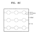
- FIGS. 8A through 8G are diagrams illustrating a method of fabricating a thin film solar cell having the first electrode 310 as shown in FIGS. 4A and 5A , according to another exemplary embodiment.
- first,” “second,” and the like, “primary,” “secondary,” and the like, as used herein do not denote any order, quantity, or importance, but rather are used to distinguish one element, region, component, layer, or section from another.
- the terms “front”, “back”, “bottom”, and/or “top” are used herein, unless otherwise noted, merely for convenience of description, and are not limited to any one position or spatial orientation.
- the endpoints of all ranges directed to the same component or property are inclusive of the endpoint and independently combinable, e.g., ranges of “up to about 25 wt. %, or, more specifically, about 5 wt. % to about 20 wt. %,” is inclusive of the endpoints and all intermediate values of the ranges of “about 5 wt. % to about 25 wt. %,” etc.
- the modifier “about” used in connection with a quantity is inclusive of the stated value and has the meaning dictated by the context (e.g., includes the degree of error associated with measurement of the particular quantity).
- FIG. 1A is a perspective view showing a schematic structure of a thin film solar cell according to an embodiment
- FIG. 1B is a cross-sectional view of the thin film solar cell of FIG. 1A
- FIG. 1C is an expanded cross-sectional view of a portion of the thin film solar cell of FIG. 1A .
- a pair of support pillars 11 which are disposed as support structures, are disposed on a substrate 10 with a selected distance therebetween, so as to support both lower ends of a unit solar cell structure 20 .
- the unit solar cell structure 20 includes a heating element 21 (hereinafter, also referred to as a first electrode, which functions as a lower electrode), a photoelectric conversion layer 22 disposed on the heating element 21 , and an upper electrode 23 (hereinafter, also referred to as a second electrode) disposed on the photoelectric conversion layer 22 . Both ends of the heating element 21 are disposed on the top surfaces of the support pillars 11 .
- the heating element 21 comprises W, Mo, SiC, or the like, or a combination comprising at least one of the foregoing materials, and functions as a lower electrode or a first electrode.
- the second electrode 23 comprises a transparent conductive material such as indium tin oxide (ITO) or a transparent conductive oxide (TCO).
- ITO indium tin oxide
- TCO transparent conductive oxide
- the photoelectric conversion layer 22 disposed between the heating element 21 and the second electrode 23 , includes a first semiconductor layer 22 a , which comprises an n-type or a p-type semiconductor material, and a second semiconductor layer 22 b , which comprises a p-type or an n-type semiconductor material.
- the first and second semiconductor layers 22 a and 22 b can comprise silicon (Si), germanium (Ge), a III-V compound, a II-VI compound, or the like, or a combination comprising at least one of the foregoing materials.
- the disclosed embodiments are not limited to the materials forming the photoelectric conversion layer 22 , or a stacked structure of the photoelectric conversion layer 22 .
- descriptions of commercially available processes and elements for the fabrication of solar cells are omitted in the descriptions of the embodiments for clarity.
- the silicon will be described as a representative semiconductor material.
- the first semiconductor layer 22 a which is disposed on heating element 21 , comprises a polycrystalline material
- the second semiconductor layer 22 b which is disposed on the first semiconductor layer 22 a
- an intrinsic semiconductor layer for example, an intrinsic semiconductor silicon layer
- the second semiconductor layer 22 b can comprise an amorphous material.
- FIG. 2A is a perspective view showing a structure for applying a voltage to heating element 21 , which is shown in FIG. 1A , in the crystallization process of the first semiconductor layer 22 a , according to another embodiment.
- heating element 21 includes a heating portion 21 a , and terminals 21 b on both ends of the heating portion 21 a .
- the terminals 21 b are disposed on the support pillars 11 .
- the heating portion 21 a when a voltage is applied through both of the terminals 21 b , the heating portion 21 a generates Joule heat.
- the Joule heat melts the first semiconductor layer 22 a , which is disposed on the heating portion 21 a in an amorphous state, and upon cooling the first semiconductor layer 22 a is crystallized.
- initial crystal nuclei are formed near to the support pillars 11 , where heat is absorbed by the substrate 10 .
- a crystalline layer may be grown on the heating element 21 directly using the heat generated from the heating element 21 .
- FIG. 2B shows a heating element 21 ′ according to another embodiment.
- the heating element 21 ′ includes two unit heating portions 21 a ′, which are substantially parallel with each other. End portions 21 c of the unit heating portions 21 a ′ are connected to each other and disposed on one of the support pillars 11 , and the other end portions 21 b ′ of the unit heating portions 21 a ′ are separated from each other and disposed on another of the support pillars 11 .
- the unit heating portions 21 a ′ when a voltage is applied to the end portions 21 b ′, the unit heating portions 21 a ′ generate heat that is absorbed through the support pillar 11 into the substrate 10 .
- FIG. 3A is a perspective view of a portion of heating element 210 according to another embodiment
- FIG. 3B is a cross-sectional view of the heating element 210 shown in FIG. 3A , taken along line A-A′ shown in FIG. 3A
- the heating element 210 has a support structure for preventing support pillars 110 from being thermally shocked or thermally damaged due to the heat generated from heating portions 211 of the heating element 210 .
- the heating element 210 includes the heating portions 211 extending in a selected direction, and extensions 212 extending from both sides of the heating portions 211 in direction different from the direction of the heating portions 211 .
- the extensions 212 can extend from both sides of the heating portions 211 in a direction that is at a right angle to the direction in which the heating portions 211 extend, and support plates 213 can be disposed under end portions of the extensions 212 .
- the support pillars 110 which can have a conical shape with a selected height and with a flat top surface, are disposed under each of the support plates 213 .
- FIG. 3C is an optical photograph showing the heat distribution in the heating element 210 shown in FIGS. 3A and 3B .
- the heating portions 211 that are arranged in a straight line are bright, and the extensions 212 are dark. Therefore, it can be observed that some of the heat is absorbed by the extensions 212 .
- FIG. 4A shows a perspective view of a portion of heating element 310 , in which support plates 313 are disposed between heating portions 311 , according to another embodiment
- FIG. 4B is a cross-sectional view of the heating element 310 of FIG. 4A , taken along line B-B′.
- the heating element 310 includes the heating portions 311 that have a high resistance and thin bar shapes, and support plates 313 that have a low resistance, disk shapes, and are configured between the heating portions 311 .
- a plurality of support pillars 110 which comprise a cone having a flat top surface, are located under the support plates 313 .
- FIG. 4C is an optical photograph showing the heat distribution in an exemplary embodiment of the heating element 310 , as shown in FIGS.
- FIG. 4C bright portions, the heating portions 311 , are observed between the support plates 313 , which are dark disks in FIG. 4C .
- the support plates 313 and the heating portions 311 are electrically arranged in a row, and the heating portions 311 have relatively high resistance, thus generate heat.
- the heating element is used as a heat source in a process of poly-crystallizing an amorphous semiconductor material, such as for example, amorphous silicon, during the processes of fabricating the solar cell, and is used as the first electrode in the lower portion of a completed solar cell, the completed solar cell having a PN junction diode or a PIN junction diode.
- the first electrode as the heat source, is separated from the substrate by a support structure, such as the support pillar, the thermal shock applied to the substrate from the heating element can be efficiently reduced. Therefore, the crystallization temperature, that is, the temperature established by the heat generated by the heating element, is not limited by the properties of the substrate material. Accordingly, using the above described heating element, the amorphous silicon can be melted at a temperature of 1000° C. or higher, and thus, a polycrystalline semiconductor layer of an excellent quality can be obtained.
- FIG. 5A is a schematic perspective view of a solar cell using a plurality of the heating elements 310 as the first electrodes in a lower portion of a solar cell.
- FIG. 5B schematically shows a layout of the first electrode 310 in the lower portion of the solar cell, and a second electrode 330 in an upper portion of the solar cell.
- FIGS. 5C and 5D are cross-sectional views showing the solar cell of FIG. 5A , taken along lines C-C′ and D-D′, respectively.
- FIG. 5E is an expanded cross-sectional view of a portion of the solar cell of FIG. 5A .
- FIG. 5F and FIG. 5G also show expanded views of portions of the solar cell depicted in FIG. 5A as is indicated in FIG. 5A .
- the plurality of first electrodes 310 are arranged in a striped configuration so as to be substantially parallel with each other.
- the plurality of second electrodes 330 comprise a grating-like structure, which includes disk portions 333 corresponding to the support plates 313 of the first electrodes 310 , and connecting portions 331 and 332 in four directions around the disk portions 333 to connect the disk portions 333 to each other, and the connecting portions 331 , which correspond to the heating portions 311 of the first electrodes 310 .
- a photoelectric conversion layer 320 having a PN or a PIN junction structure, is located between the overlapping portions of the first electrodes 310 and the second electrodes 330 .
- FIG. 5C shows a stacked structure of the solar cell in a first direction, that is, a length direction.
- FIG. 5E shows an expanded view of a portion of the stacked structure of the solar cell shown in FIG. 5C , which has a sandwich-type structure, including the first electrodes 310 , the photoelectric conversion layer 320 , and the second electrodes 330 .
- the sandwich-type structure is supported by the support pillars 110 of the first electrodes 310 so that the support pillars 110 are located under the sandwich-type structure.
- FIG. 5C shows a sandwich-type structure of the solar cell in a first direction, that is, a length direction.
- FIG. 5E shows an expanded view of a portion of the stacked structure of the solar cell shown in FIG. 5C , which has a sandwich-type structure, including the first electrodes 310 , the photoelectric conversion layer 320 , and the second electrodes 330 .
- the sandwich-type structure is supported by the support pillars 110 of the first electrodes
- the sandwich-type structure includes the first electrodes 310 , the photoelectric conversion layer 320 , and the second electrodes 330 , and is located on the support pillars 110 of the first electrodes 310 .
- the first electrodes 310 are located only on upper portions of the support pillars 110 , and thus, a bottom surface of the photoelectric conversion layer 320 is exposed in portions of the photoelectric conversion layer 320 , which are between the support pillars 110 .
- the above-described structure is a solar cell with a large capacity and a large area, wherein unit solar cells can be arranged in arrays.
- FIGS. 6A through 6E illustrate a process of fabricating a solar cell having a first electrode, such as first electrode 21 , which is shown in FIG. 2A , according to an embodiment.
- a sacrificial layer 11 ′ and a heating material layer 21 ′ which comprise a heating material, are disposed on the substrate 10 .
- the sacrificial layer 11 ′ comprises, for example, SiO 2 , and can be disposed using a chemical vapor deposition (CVD) method, for example.
- the heating material layer 21 ′ comprises a material such as W, Mo, SiC, or the like, or a combination comprising at least one of the foregoing materials, for example, and can be disposed using a physical vapor deposition (PVD) method, such as by sputtering, electron beam deposition, or the like, for example.
- PVD physical vapor deposition
- the heating material layer 21 ′ and the sacrificial layer 11 ′ are patterned to obtain the heating element 21 shown in FIG. 2A , and support pillars 11 , which support the heating element 21 .
- the heating material layer 21 ′ is patterned to obtain the heating element 21 , and then, the sacrificial layer 11 ′ under the heating element 21 is wet-etched using the heating element 21 as a mask to obtain the support pillars 11 from the remaining portions of the etched pattern.
- an amorphous semiconductor material for example, amorphous silicon (a-Si) 22 a ′, is disposed on the first electrode 21 using CVD.
- amorphous silicon layer is also disposed on a surface of the substrate 10 and on the heating element 21 .
- a voltage is applied to the heating element 21 for a selected time to generate Joule heat and to melt the a-Si 22 a ′ on the heating element 21 .
- the melted a-Si 22 a ′ starts to solidify when the heating element 21 stops generating heat, and then, a crystallization of the a-Si 22 a ′ occurs.
- crystal nuclei form around the support pillars 11 , which absorb heat, and thus, a crystal growth proceeds toward a center portion of the heating element 21 in a direction parallel to the heating element 21 .
- a polycrystalline semiconductor layer for example, a first semiconductor layer 22 a formed of polycrystalline silicon can be obtained.
- a coalescence boundary, on which the crystals growing from both ends of the heating element 21 are combined, can exist at the center portion of the heating element 21 .
- a material that is different from that of the first semiconductor layer 22 a is disposed to form a second semiconductor layer 22 b , and a transparent conductive material, for example, an ITO layer, is disposed on the second semiconductor layer 22 b to form a second electrode 23 .
- the fabrication of the desired solar cell is completed.
- the material for the second semiconductor layer 22 b , and the material for the second electrode 23 can be disposed on the substrate 10 , however, the materials disposed directly on the substrate are electrically separated from the first and second electrodes 21 and 23 and may have no function in the solar cell.
- the first electrode is used as the heat source for poly-crystallizing the semiconductor layer on the first electrode in the solar cell.
- the polycrystalline semiconductor for example, polycrystalline silicon, polycrystalline germanium, or the like, or a combination comprising at least one of the foregoing materials, can be fabricated by local heat generation by the first electrode. Accordingly, the polycrystalline semiconductor layer can be obtained without using an additional thermal processing apparatus or performing an additional process.
- the crystallization process is performed using a first electrode having a narrow configuration, which generates heat, the substrate is separated from the first electrode by the support structure, for example, the support pillars, and thus, the temperature of the substrate can be maintained at about room temperature.
- the heating element or the first electrodes according to the embodiments may be formed in various shapes, for example, a plate shape, a core-shell, a band-like shape, a rod-like shape, a wire-like shape, or a thread shape.
- the second semiconductor layer 22 b is disposed after performing the process shown in FIG. 6D .
- an n-type or a p-type semiconductor material layer and a p-type or an n-type first semiconductor material are sequentially disposed, and after that, the poly-crystallization process shown in FIG. 6D may be performed.
- the first semiconductor layer 22 a and the second semiconductor layer 22 b are thermally treated together. Therefore, in a case where a sufficient amount of heat is supplied to the first and second semiconductor layers 22 a and 22 b , both of the first and second semiconductor layers 22 a and 22 b may have a polycrystalline structure.
- the polycrystalline silicon and the amorphous silicon may mix in the second semiconductor layer 22 b , or the second semiconductor layer 22 b may have a micro-crystalline structure comprising small size crystals.
- an intrinsic semiconductor material layer may be disposed before disposing the second semiconductor layer 22 b . Then, a solar cell having a PIN junction structure can be obtained by disposing the intrinsic semiconductor material layer.
- FIG. 7A is a longitudinal cross-sectional view of the photoelectric conversion layer of FIG. 6E , taken along line E-E′.
- the edges of the stacked layers are not aligned with each other, and the surfaces of the stacked layers are rounded so that the entire surface of the stacked structure can be curved.
- the first and second semiconductor layers 22 a and 22 b disposed using CVD, are not only disposed on the top surface of the heating element 21 , but may be disposed on a side surface of the heating element 21 , to which a gas contacts. As shown in FIG.
- a source gas may contact all surfaces of the heating element 21 in the CVD process, and thus, the first and second semiconductor layers 22 a and 22 b may be disposed so as to completely surround the heating element 21 .
- the stacked structure on the heating element 21 may vary according to process conditions, and that disclosed is not limited to the stacked structure shown.
- FIGS. 8A through 8G illustrate a method of fabricating a solar cell having the first electrode 310 shown in FIGS. 4A and 5A , according to another embodiment.
- a sacrificial layer 110 ′ and a heating material layer 310 ′ are disposed on a substrate 10 .
- the sacrificial layer 110 ′ comprises, for example, SiO 2 , and can be disposed using by CVD.
- the heating material layer 310 ′ comprises a material such as W, Mo, or SiC, and can be disposed using PVD, for example, thus by sputtering or electron beam deposition, for example.
- the heating material layer 310 ′ is patterned using a dry-etching method using a mask, to form a plurality of heating elements 310 .
- Each heating element 310 includes heating portions 311 and support plates 313 , the support plates having a disk shape, and are configured between the heating portions 311 , in a substantially parallel configuration.
- each of the heating portions 311 between the support plates 313 correspond to a unit solar cell.
- an amorphous silicon layer 320 a ′ which is a n-type or a p-type semiconductor layer, covers the heating element 310 , and the sacrificial layer 110 ′ is disposed using CVD.
- electric current is supplied to each of the heating elements 310 so as to melt the a-Si, that is, the first semiconductor material, on the heating element 310 , and after that, the melted semiconductor material crystallizes to form the polycrystalline silicon.
- the polycrystalline silicon may be formed on the heating portions 311 , which have a high resistance value, and the a-Si may remain on the other portions of the heating elements 310 , where the first electrodes 311 are not formed.
- a p-type or an n-type amorphous silicon layer 320 b ′ is disposed on the p-type or n-type amorphous silicon layer 320 a ′, which is crystallized locally, using the CVD method.
- a transparent conductive layer such as the ITO layer is formed on the p-type or n-type silicon layer 320 b ′, and is patterned to form second electrodes 330 in a grating-like configuration.
- the second electrodes can have a grating-like shape and are shown in FIGS. 5A and 5B .
- the structure under the second electrodes 330 is etched by a wet-etchant using the grating-shaped second electrodes 330 as a mask.
- the sacrificial layer 110 ′ under the heating element 310 is also etched, and the sacrificial layer 110 ′ under the support plates 313 , having a relatively larger area than any other portions, are locally etched, for example, and may be undercut-etched.
- the sacrificial layer 110 ′ is removed, except for the support pillars 110 under the support plates 313 , by selecting the etching time appropriately.
- a diameter of each of the support plates 313 and a width of each of the heating portions 311 can be selected when designing the solar cell in consideration of the degree of etching so that the sacrificial layer 110 ′ remains only under the support plates 313 .
Landscapes
- Engineering & Computer Science (AREA)
- Power Engineering (AREA)
- Condensed Matter Physics & Semiconductors (AREA)
- Electromagnetism (AREA)
- General Physics & Mathematics (AREA)
- Computer Hardware Design (AREA)
- Physics & Mathematics (AREA)
- Microelectronics & Electronic Packaging (AREA)
- Manufacturing & Machinery (AREA)
- Chemical & Material Sciences (AREA)
- Crystallography & Structural Chemistry (AREA)
- Life Sciences & Earth Sciences (AREA)
- Sustainable Development (AREA)
- Sustainable Energy (AREA)
- Photovoltaic Devices (AREA)
- Recrystallisation Techniques (AREA)
Abstract
Description
Claims (9)
Applications Claiming Priority (2)
| Application Number | Priority Date | Filing Date | Title |
|---|---|---|---|
| KR1020080020584A KR20090095314A (en) | 2008-03-05 | 2008-03-05 | Crystallization method of amorphous layer and thin film solar cell and fabrication method of the cell adopting the crystallization method |
| KR10-2008-0020584 | 2008-03-05 |
Publications (2)
| Publication Number | Publication Date |
|---|---|
| US20090223557A1 US20090223557A1 (en) | 2009-09-10 |
| US8324498B2 true US8324498B2 (en) | 2012-12-04 |
Family
ID=41052355
Family Applications (1)
| Application Number | Title | Priority Date | Filing Date |
|---|---|---|---|
| US12/270,588 Expired - Fee Related US8324498B2 (en) | 2008-03-05 | 2008-11-13 | Method of forming crystalline layer, and thin film solar cell and method of fabricating the solar cell adopting the method of forming crystalline layer |
Country Status (2)
| Country | Link |
|---|---|
| US (1) | US8324498B2 (en) |
| KR (1) | KR20090095314A (en) |
Families Citing this family (13)
| Publication number | Priority date | Publication date | Assignee | Title |
|---|---|---|---|---|
| KR101338350B1 (en) * | 2007-07-16 | 2013-12-31 | 삼성전자주식회사 | Method for forming nanostructure or poly silicone using microheater, nanostructure or poly silicone formed by the method and electronic device using the same |
| KR101318292B1 (en) * | 2007-11-30 | 2013-10-18 | 삼성전자주식회사 | Microheater, microheater array, method for manufacturing the same and electronic device using the same |
| KR20090095314A (en) | 2008-03-05 | 2009-09-09 | 삼성전자주식회사 | Crystallization method of amorphous layer and thin film solar cell and fabrication method of the cell adopting the crystallization method |
| KR20090102031A (en) * | 2008-03-25 | 2009-09-30 | 삼성전자주식회사 | Micro-heater array, method for fabricating pn-junction using the same, and pn-junction device having micro-heater array and pn-junction |
| KR20090122083A (en) * | 2008-05-23 | 2009-11-26 | 삼성전자주식회사 | Microheater, microheater array, method for manufacturing the same and electronic device using the same |
| KR20090128006A (en) * | 2008-06-10 | 2009-12-15 | 삼성전자주식회사 | Micro-heaters, micro-heater arrays, method for manufacturing the same and method for forming patterns using the same |
| KR20100086799A (en) * | 2009-01-23 | 2010-08-02 | 삼성전자주식회사 | Micro-heaters and methods for manufacturing the same |
| KR20100086735A (en) * | 2009-01-23 | 2010-08-02 | 삼성전자주식회사 | Method for forming silicon film, method for forming pn junction and pn junction formed using the same |
| US9177761B2 (en) * | 2009-08-25 | 2015-11-03 | Semiconductor Energy Laboratory Co., Ltd. | Plasma CVD apparatus, method for forming microcrystalline semiconductor film and method for manufacturing semiconductor device |
| KR101722903B1 (en) * | 2009-08-25 | 2017-04-04 | 가부시키가이샤 한도오따이 에네루기 켄큐쇼 | Method of manufacturing photoelectric conversion device |
| FR2959870B1 (en) * | 2010-05-06 | 2012-05-18 | Commissariat Energie Atomique | PHOTOVOLTAIC CELL COMPRISING A ZONE SUSPENDED BY A CONDUCTIVE PATTERN AND METHOD OF MAKING THE SAME. |
| KR20110136180A (en) * | 2010-06-14 | 2011-12-21 | 삼성전자주식회사 | Method of forming electrode and method of manufacturing solar cell using the same |
| CN105097547A (en) * | 2015-06-01 | 2015-11-25 | 合肥京东方光电科技有限公司 | Polycrystalline silicon thin film transistor, manufacturing method thereof, array substrate and manufacturing method thereof |
Citations (22)
| Publication number | Priority date | Publication date | Assignee | Title |
|---|---|---|---|---|
| US4180414A (en) * | 1978-07-10 | 1979-12-25 | Optical Coating Laboratory, Inc. | Concentrator solar cell array module |
| US4254429A (en) * | 1978-07-08 | 1981-03-03 | Shunpei Yamazaki | Hetero junction semiconductor device |
| US4487989A (en) * | 1983-07-25 | 1984-12-11 | Atlantic Richfield Company | Contact for solar cell |
| US5034068A (en) | 1990-02-23 | 1991-07-23 | Spectrolab, Inc. | Photovoltaic cell having structurally supporting open conductive back electrode structure, and method of fabricating the cell |
| US5185042A (en) * | 1991-08-01 | 1993-02-09 | Trw Inc. | Generic solar cell array using a printed circuit substrate |
| JPH06204142A (en) | 1992-12-28 | 1994-07-22 | Tonen Corp | Manufacture of silicon crystal film by thermal cvd |
| JPH07106611A (en) | 1993-09-29 | 1995-04-21 | Tonen Corp | Fabrication of bsf solar cell |
| US5853497A (en) | 1996-12-12 | 1998-12-29 | Hughes Electronics Corporation | High efficiency multi-junction solar cells |
| JPH11150283A (en) | 1997-11-19 | 1999-06-02 | Tdk Corp | Manufacture of polycrystalline silicon thin film |
| JP2001068422A (en) | 1999-08-24 | 2001-03-16 | Junichi Hanna | Manufacture of semiconductor base material |
| US6232546B1 (en) * | 1997-07-30 | 2001-05-15 | The Charles Stark Draper Laboratory, Inc. | Microcavity apparatus and systems for maintaining a microcavity over a macroscale area |
| US20030075213A1 (en) | 2001-10-23 | 2003-04-24 | Chen Leon L.C. | Stationary photovoltaic array module design for solar electric power generation systems |
| US20040166681A1 (en) * | 2002-12-05 | 2004-08-26 | Iles Peter A. | High efficiency, monolithic multijunction solar cells containing lattice-mismatched materials and methods of forming same |
| US6896780B2 (en) | 2001-09-12 | 2005-05-24 | Electronics And Telecommunications Research Institute | Microelectrode, microelectrode array and method for manufacturing the microelectrode |
| US7217882B2 (en) | 2002-05-24 | 2007-05-15 | Cornell Research Foundation, Inc. | Broad spectrum solar cell |
| US7329361B2 (en) | 2003-10-29 | 2008-02-12 | International Business Machines Corporation | Method and apparatus for fabricating or altering microstructures using local chemical alterations |
| US20080245400A1 (en) | 2007-04-09 | 2008-10-09 | Amberwave Systems Corporation | Nitride-based multi-junction solar cell modules and methods for making the same |
| US20090020760A1 (en) | 2007-07-16 | 2009-01-22 | Samsung Electronics Co., Ltd. | Methods for forming materials using micro-heaters and electronic devices including such materials |
| US20090223557A1 (en) | 2008-03-05 | 2009-09-10 | Samsung Electronics Co., Ltd. | Method of forming crystalline layer, and thin film solar cell and method of fabricating the solar cell adopting the method of forming crystalline layer |
| US20090250112A1 (en) | 2008-04-07 | 2009-10-08 | Samsung Electronics Co., Ltd. | Solar cell and method for manufacturing the same |
| US20100187662A1 (en) | 2009-01-23 | 2010-07-29 | Samsung Electronics Co., Ltd. | Method for forming silicon film, method for forming pn junction and pn junction formed using the same |
| US20100302337A1 (en) | 2009-05-29 | 2010-12-02 | Xerox Corporation | Heating element incorporating an array of transistor micro-heaters for digital image marking |
Family Cites Families (7)
| Publication number | Priority date | Publication date | Assignee | Title |
|---|---|---|---|---|
| US245400A (en) * | 1881-08-09 | Steam-boiler | ||
| US250112A (en) * | 1881-11-29 | Snap-hook | ||
| US302337A (en) * | 1884-07-22 | jackson | ||
| US187662A (en) * | 1877-02-20 | Improvement in window-cornices | ||
| US75213A (en) * | 1868-03-03 | Improved carriage-wheel | ||
| US223557A (en) * | 1880-01-13 | houston | ||
| US20760A (en) * | 1858-06-29 | Improvement in apparatus for rectifying |
-
2008
- 2008-03-05 KR KR1020080020584A patent/KR20090095314A/en not_active Application Discontinuation
- 2008-11-13 US US12/270,588 patent/US8324498B2/en not_active Expired - Fee Related
Patent Citations (22)
| Publication number | Priority date | Publication date | Assignee | Title |
|---|---|---|---|---|
| US4254429A (en) * | 1978-07-08 | 1981-03-03 | Shunpei Yamazaki | Hetero junction semiconductor device |
| US4180414A (en) * | 1978-07-10 | 1979-12-25 | Optical Coating Laboratory, Inc. | Concentrator solar cell array module |
| US4487989A (en) * | 1983-07-25 | 1984-12-11 | Atlantic Richfield Company | Contact for solar cell |
| US5034068A (en) | 1990-02-23 | 1991-07-23 | Spectrolab, Inc. | Photovoltaic cell having structurally supporting open conductive back electrode structure, and method of fabricating the cell |
| US5185042A (en) * | 1991-08-01 | 1993-02-09 | Trw Inc. | Generic solar cell array using a printed circuit substrate |
| JPH06204142A (en) | 1992-12-28 | 1994-07-22 | Tonen Corp | Manufacture of silicon crystal film by thermal cvd |
| JPH07106611A (en) | 1993-09-29 | 1995-04-21 | Tonen Corp | Fabrication of bsf solar cell |
| US5853497A (en) | 1996-12-12 | 1998-12-29 | Hughes Electronics Corporation | High efficiency multi-junction solar cells |
| US6232546B1 (en) * | 1997-07-30 | 2001-05-15 | The Charles Stark Draper Laboratory, Inc. | Microcavity apparatus and systems for maintaining a microcavity over a macroscale area |
| JPH11150283A (en) | 1997-11-19 | 1999-06-02 | Tdk Corp | Manufacture of polycrystalline silicon thin film |
| JP2001068422A (en) | 1999-08-24 | 2001-03-16 | Junichi Hanna | Manufacture of semiconductor base material |
| US6896780B2 (en) | 2001-09-12 | 2005-05-24 | Electronics And Telecommunications Research Institute | Microelectrode, microelectrode array and method for manufacturing the microelectrode |
| US20030075213A1 (en) | 2001-10-23 | 2003-04-24 | Chen Leon L.C. | Stationary photovoltaic array module design for solar electric power generation systems |
| US7217882B2 (en) | 2002-05-24 | 2007-05-15 | Cornell Research Foundation, Inc. | Broad spectrum solar cell |
| US20040166681A1 (en) * | 2002-12-05 | 2004-08-26 | Iles Peter A. | High efficiency, monolithic multijunction solar cells containing lattice-mismatched materials and methods of forming same |
| US7329361B2 (en) | 2003-10-29 | 2008-02-12 | International Business Machines Corporation | Method and apparatus for fabricating or altering microstructures using local chemical alterations |
| US20080245400A1 (en) | 2007-04-09 | 2008-10-09 | Amberwave Systems Corporation | Nitride-based multi-junction solar cell modules and methods for making the same |
| US20090020760A1 (en) | 2007-07-16 | 2009-01-22 | Samsung Electronics Co., Ltd. | Methods for forming materials using micro-heaters and electronic devices including such materials |
| US20090223557A1 (en) | 2008-03-05 | 2009-09-10 | Samsung Electronics Co., Ltd. | Method of forming crystalline layer, and thin film solar cell and method of fabricating the solar cell adopting the method of forming crystalline layer |
| US20090250112A1 (en) | 2008-04-07 | 2009-10-08 | Samsung Electronics Co., Ltd. | Solar cell and method for manufacturing the same |
| US20100187662A1 (en) | 2009-01-23 | 2010-07-29 | Samsung Electronics Co., Ltd. | Method for forming silicon film, method for forming pn junction and pn junction formed using the same |
| US20100302337A1 (en) | 2009-05-29 | 2010-12-02 | Xerox Corporation | Heating element incorporating an array of transistor micro-heaters for digital image marking |
Non-Patent Citations (4)
| Title |
|---|
| U.S. Notice of Allowance dated Jul. 7, 2011, for cross-reference U.S. Appl. No. 12/232,711, 9 pages. |
| U.S. Office action dated Dec. 21, 2010, for cross-reference U.S. Appl. No. 12/232,711, 7 pages. |
| U.S. Office action dated Jul. 20, 2011, for cross-reference U.S. Appl. No. 12/320,924, 11 pages. |
| U.S. Office action dated Sep. 21, 2011, for cross-reference U.S. Appl. No. 12/458,665, 11 pages. |
Also Published As
| Publication number | Publication date |
|---|---|
| KR20090095314A (en) | 2009-09-09 |
| US20090223557A1 (en) | 2009-09-10 |
Similar Documents
| Publication | Publication Date | Title |
|---|---|---|
| US8324498B2 (en) | Method of forming crystalline layer, and thin film solar cell and method of fabricating the solar cell adopting the method of forming crystalline layer | |
| KR102665965B1 (en) | Solar cell and method for fabricating therefor | |
| US8258050B2 (en) | Method of making light trapping crystalline structures | |
| KR101636915B1 (en) | Semiconductor compound structure and method of manufacturing the same using graphene or carbon nanotubes, and seciconductor device including the semiconductor compound | |
| US8389388B2 (en) | Photonic device and method of making the same | |
| JP6086905B2 (en) | Solar cell and manufacturing method thereof | |
| JP2003298078A (en) | Photoelectromotive element | |
| TW201013950A (en) | Solar cell module and method for fabricating the same | |
| CN101005017B (en) | Method of forming a semiconductor thin film | |
| TW201017900A (en) | Solar cell and method for fabricating the same | |
| JP5591486B2 (en) | Silicon film formation method, pn junction formation method, and pn junction formed using the same | |
| KR20100070753A (en) | Manufacturing method of photovoltaic devices | |
| JP2004273887A (en) | Crystalline thin film semiconductor device and solar cell element | |
| US8003423B2 (en) | Method for manufacturing a poly-crystal silicon photovoltaic device using horizontal metal induced crystallization | |
| JP2010177655A (en) | Method for manufacturing back junction type solar cell | |
| US20090117683A1 (en) | Method of manufacturing single crystal substate and method of manufacturing solar cell using the same | |
| JP2013138128A (en) | Semiconductor device and manufacturing method of the same | |
| US8053854B2 (en) | Micro-heater arrays and pn-junction devices having micro-heater arrays, and methods for fabricating the same | |
| KR100847593B1 (en) | Solar cells and method for fabricating the same | |
| JP2008098464A (en) | Method of manufacturing semiconductor device | |
| TWI660075B (en) | Method for manufacturing polysilicon layer, heterojunction solar cell and manufacturing method thereof | |
| JP2004146517A (en) | Forming apparatus and forming method for crystal thin film semiconductor | |
| KR20140057715A (en) | Method of fabricating a nano pattern by using rapid thermal process to au thin layer | |
| KR101031881B1 (en) | fabricating method of a solar cell | |
| JPH02197177A (en) | Manufacture of semiconductor device |
Legal Events
| Date | Code | Title | Description |
|---|---|---|---|
| AS | Assignment |
Owner name: SAMSUNG ELECTRONICS CO., LTD., KOREA, REPUBLIC OF Free format text: ASSIGNMENT OF ASSIGNORS INTEREST;ASSIGNORS:PARK, YOUNGJUN;CHOI, JUNHEE;NAM, JUNGGYU;REEL/FRAME:021834/0550 Effective date: 20081104 |
|
| AS | Assignment |
Owner name: SAMSUNG ELECTRONICS CO., LTD., KOREA, REPUBLIC OF Free format text: ASSIGNMENT OF ASSIGNORS INTEREST;ASSIGNOR:SAMSUNG ELECTRONICS CO., LTD.;REEL/FRAME:026590/0975 Effective date: 20110711 Owner name: SAMSUNG SDI CO., LTD., KOREA, REPUBLIC OF Free format text: ASSIGNMENT OF ASSIGNORS INTEREST;ASSIGNOR:SAMSUNG ELECTRONICS CO., LTD.;REEL/FRAME:026590/0975 Effective date: 20110711 |
|
| FEPP | Fee payment procedure |
Free format text: PAYOR NUMBER ASSIGNED (ORIGINAL EVENT CODE: ASPN); ENTITY STATUS OF PATENT OWNER: LARGE ENTITY |
|
| REMI | Maintenance fee reminder mailed | ||
| LAPS | Lapse for failure to pay maintenance fees | ||
| STCH | Information on status: patent discontinuation |
Free format text: PATENT EXPIRED DUE TO NONPAYMENT OF MAINTENANCE FEES UNDER 37 CFR 1.362 |
|
| FP | Lapsed due to failure to pay maintenance fee |
Effective date: 20161204 |