US8248685B2 - Display particles for image display apparatus and image display apparatus loaded with the same - Google Patents
Display particles for image display apparatus and image display apparatus loaded with the same Download PDFInfo
- Publication number
- US8248685B2 US8248685B2 US12/814,556 US81455610A US8248685B2 US 8248685 B2 US8248685 B2 US 8248685B2 US 81455610 A US81455610 A US 81455610A US 8248685 B2 US8248685 B2 US 8248685B2
- Authority
- US
- United States
- Prior art keywords
- particles
- compound
- image display
- display
- display apparatus
- Prior art date
- Legal status (The legal status is an assumption and is not a legal conclusion. Google has not performed a legal analysis and makes no representation as to the accuracy of the status listed.)
- Expired - Fee Related, expires
Links
- 239000002245 particle Substances 0.000 title claims abstract description 294
- 229910044991 metal oxide Inorganic materials 0.000 claims abstract description 80
- 150000004706 metal oxides Chemical class 0.000 claims abstract description 80
- 150000001875 compounds Chemical class 0.000 claims abstract description 53
- 229920005989 resin Polymers 0.000 claims abstract description 52
- 239000011347 resin Substances 0.000 claims abstract description 52
- 229940126062 Compound A Drugs 0.000 claims abstract description 38
- NLDMNSXOCDLTTB-UHFFFAOYSA-N Heterophylliin A Natural products O1C2COC(=O)C3=CC(O)=C(O)C(O)=C3C3=C(O)C(O)=C(O)C=C3C(=O)OC2C(OC(=O)C=2C=C(O)C(O)=C(O)C=2)C(O)C1OC(=O)C1=CC(O)=C(O)C(O)=C1 NLDMNSXOCDLTTB-UHFFFAOYSA-N 0.000 claims abstract description 38
- -1 acryloyloxy group Chemical group 0.000 claims abstract description 21
- 239000003086 colorant Substances 0.000 claims abstract description 21
- 239000000463 material Substances 0.000 claims abstract description 21
- 125000000217 alkyl group Chemical group 0.000 claims abstract description 20
- 125000004432 carbon atom Chemical group C* 0.000 claims abstract description 19
- XUIMIQQOPSSXEZ-UHFFFAOYSA-N Silicon Chemical group [Si] XUIMIQQOPSSXEZ-UHFFFAOYSA-N 0.000 claims abstract description 17
- 229910052710 silicon Inorganic materials 0.000 claims abstract description 15
- RTAQQCXQSZGOHL-UHFFFAOYSA-N Titanium Chemical group [Ti] RTAQQCXQSZGOHL-UHFFFAOYSA-N 0.000 claims abstract description 13
- 238000006068 polycondensation reaction Methods 0.000 claims abstract description 12
- 229910052719 titanium Inorganic materials 0.000 claims abstract description 12
- 125000001997 phenyl group Chemical group [H]C1=C([H])C([H])=C(*)C([H])=C1[H] 0.000 claims abstract description 6
- 125000003700 epoxy group Chemical group 0.000 claims abstract description 5
- 239000010410 layer Substances 0.000 claims description 87
- 239000000758 substrate Substances 0.000 claims description 87
- 238000000034 method Methods 0.000 claims description 63
- BOTDANWDWHJENH-UHFFFAOYSA-N Tetraethyl orthosilicate Chemical compound CCO[Si](OCC)(OCC)OCC BOTDANWDWHJENH-UHFFFAOYSA-N 0.000 claims description 26
- 229910052751 metal Inorganic materials 0.000 claims description 25
- 239000002184 metal Substances 0.000 claims description 25
- 239000010419 fine particle Substances 0.000 claims description 21
- 239000000203 mixture Substances 0.000 claims description 21
- GWEVSGVZZGPLCZ-UHFFFAOYSA-N Titan oxide Chemical compound O=[Ti]=O GWEVSGVZZGPLCZ-UHFFFAOYSA-N 0.000 claims description 20
- 230000005684 electric field Effects 0.000 claims description 18
- YYLGKUPAFFKGRQ-UHFFFAOYSA-N dimethyldiethoxysilane Chemical compound CCO[Si](C)(C)OCC YYLGKUPAFFKGRQ-UHFFFAOYSA-N 0.000 claims description 14
- 239000012044 organic layer Substances 0.000 claims description 14
- 238000002156 mixing Methods 0.000 claims description 8
- 239000011164 primary particle Substances 0.000 claims description 7
- 239000006229 carbon black Substances 0.000 claims description 6
- 239000000843 powder Substances 0.000 claims description 6
- XGZNHFPFJRZBBT-UHFFFAOYSA-N ethanol;titanium Chemical compound [Ti].CCO.CCO.CCO.CCO XGZNHFPFJRZBBT-UHFFFAOYSA-N 0.000 claims description 5
- OGIDPMRJRNCKJF-UHFFFAOYSA-N titanium oxide Inorganic materials [Ti]=O OGIDPMRJRNCKJF-UHFFFAOYSA-N 0.000 claims description 5
- CPUDPFPXCZDNGI-UHFFFAOYSA-N triethoxy(methyl)silane Chemical compound CCO[Si](C)(OCC)OCC CPUDPFPXCZDNGI-UHFFFAOYSA-N 0.000 claims description 5
- MNFGEHQPOWJJBH-UHFFFAOYSA-N diethoxy-methyl-phenylsilane Chemical compound CCO[Si](C)(OCC)C1=CC=CC=C1 MNFGEHQPOWJJBH-UHFFFAOYSA-N 0.000 claims description 4
- ZEIWWVGGEOHESL-UHFFFAOYSA-N methanol;titanium Chemical compound [Ti].OC.OC.OC.OC ZEIWWVGGEOHESL-UHFFFAOYSA-N 0.000 claims description 3
- 239000000049 pigment Substances 0.000 claims description 3
- LFQCEHFDDXELDD-UHFFFAOYSA-N tetramethyl orthosilicate Chemical compound CO[Si](OC)(OC)OC LFQCEHFDDXELDD-UHFFFAOYSA-N 0.000 claims description 3
- DOYKFSOCSXVQAN-UHFFFAOYSA-N 3-[diethoxy(methyl)silyl]propyl 2-methylprop-2-enoate Chemical compound CCO[Si](C)(OCC)CCCOC(=O)C(C)=C DOYKFSOCSXVQAN-UHFFFAOYSA-N 0.000 claims description 2
- ITJHDXSUEINCDE-UHFFFAOYSA-N CCO[Ti](C)(OCC)OCC Chemical compound CCO[Ti](C)(OCC)OCC ITJHDXSUEINCDE-UHFFFAOYSA-N 0.000 claims description 2
- GUWTUQVATYZAIT-UHFFFAOYSA-N CO[Ti](C)(C)OC Chemical compound CO[Ti](C)(C)OC GUWTUQVATYZAIT-UHFFFAOYSA-N 0.000 claims description 2
- ZUEKXCXHTXJYAR-UHFFFAOYSA-N tetrapropan-2-yl silicate Chemical compound CC(C)O[Si](OC(C)C)(OC(C)C)OC(C)C ZUEKXCXHTXJYAR-UHFFFAOYSA-N 0.000 claims description 2
- 239000012463 white pigment Substances 0.000 claims description 2
- VYPSYNLAJGMNEJ-UHFFFAOYSA-N Silicium dioxide Chemical compound O=[Si]=O VYPSYNLAJGMNEJ-UHFFFAOYSA-N 0.000 description 68
- FFUAGWLWBBFQJT-UHFFFAOYSA-N hexamethyldisilazane Chemical compound C[Si](C)(C)N[Si](C)(C)C FFUAGWLWBBFQJT-UHFFFAOYSA-N 0.000 description 42
- 239000003795 chemical substances by application Substances 0.000 description 26
- 239000000377 silicon dioxide Substances 0.000 description 20
- 230000008569 process Effects 0.000 description 19
- 230000004888 barrier function Effects 0.000 description 12
- 239000000243 solution Substances 0.000 description 12
- 125000004429 atom Chemical group 0.000 description 11
- WYTZZXDRDKSJID-UHFFFAOYSA-N (3-aminopropyl)triethoxysilane Chemical compound CCO[Si](OCC)(OCC)CCCN WYTZZXDRDKSJID-UHFFFAOYSA-N 0.000 description 9
- 238000004519 manufacturing process Methods 0.000 description 9
- 239000000178 monomer Substances 0.000 description 9
- 239000006185 dispersion Substances 0.000 description 8
- 239000000047 product Substances 0.000 description 8
- 230000003252 repetitive effect Effects 0.000 description 8
- XLOMVQKBTHCTTD-UHFFFAOYSA-N Zinc monoxide Chemical compound [Zn]=O XLOMVQKBTHCTTD-UHFFFAOYSA-N 0.000 description 7
- 230000000052 comparative effect Effects 0.000 description 7
- 239000010408 film Substances 0.000 description 7
- 238000004381 surface treatment Methods 0.000 description 7
- 239000004925 Acrylic resin Substances 0.000 description 6
- 230000002093 peripheral effect Effects 0.000 description 6
- 229920000642 polymer Polymers 0.000 description 6
- LVTJOONKWUXEFR-FZRMHRINSA-N protoneodioscin Natural products O(C[C@@H](CC[C@]1(O)[C@H](C)[C@@H]2[C@]3(C)[C@H]([C@H]4[C@@H]([C@]5(C)C(=CC4)C[C@@H](O[C@@H]4[C@H](O[C@H]6[C@@H](O)[C@@H](O)[C@@H](O)[C@H](C)O6)[C@@H](O)[C@H](O[C@H]6[C@@H](O)[C@@H](O)[C@@H](O)[C@H](C)O6)[C@H](CO)O4)CC5)CC3)C[C@@H]2O1)C)[C@H]1[C@H](O)[C@H](O)[C@H](O)[C@@H](CO)O1 LVTJOONKWUXEFR-FZRMHRINSA-N 0.000 description 6
- 238000002834 transmittance Methods 0.000 description 6
- 239000000654 additive Substances 0.000 description 5
- 229910052782 aluminium Inorganic materials 0.000 description 5
- 230000015556 catabolic process Effects 0.000 description 5
- 238000006243 chemical reaction Methods 0.000 description 5
- 238000000576 coating method Methods 0.000 description 5
- 238000006731 degradation reaction Methods 0.000 description 5
- 150000002736 metal compounds Chemical class 0.000 description 5
- 239000012756 surface treatment agent Substances 0.000 description 5
- 125000000391 vinyl group Chemical group [H]C([*])=C([H])[H] 0.000 description 5
- 229920002554 vinyl polymer Polymers 0.000 description 5
- XLYOFNOQVPJJNP-UHFFFAOYSA-N water Substances O XLYOFNOQVPJJNP-UHFFFAOYSA-N 0.000 description 5
- 230000015572 biosynthetic process Effects 0.000 description 4
- 239000011248 coating agent Substances 0.000 description 4
- 239000004431 polycarbonate resin Substances 0.000 description 4
- 229920005668 polycarbonate resin Polymers 0.000 description 4
- 239000000523 sample Substances 0.000 description 4
- 238000000926 separation method Methods 0.000 description 4
- 150000003377 silicon compounds Chemical class 0.000 description 4
- 239000002904 solvent Substances 0.000 description 4
- 239000004094 surface-active agent Substances 0.000 description 4
- 239000012780 transparent material Substances 0.000 description 4
- 238000011144 upstream manufacturing Methods 0.000 description 4
- 235000014692 zinc oxide Nutrition 0.000 description 4
- 239000011787 zinc oxide Substances 0.000 description 4
- 229910000859 α-Fe Inorganic materials 0.000 description 4
- QTBSBXVTEAMEQO-UHFFFAOYSA-N Acetic acid Chemical compound CC(O)=O QTBSBXVTEAMEQO-UHFFFAOYSA-N 0.000 description 3
- 239000000853 adhesive Substances 0.000 description 3
- 230000001070 adhesive effect Effects 0.000 description 3
- XAGFODPZIPBFFR-UHFFFAOYSA-N aluminium Chemical compound [Al] XAGFODPZIPBFFR-UHFFFAOYSA-N 0.000 description 3
- 239000007822 coupling agent Substances 0.000 description 3
- 230000000694 effects Effects 0.000 description 3
- 125000001495 ethyl group Chemical group [H]C([H])([H])C([H])([H])* 0.000 description 3
- 239000011521 glass Substances 0.000 description 3
- 230000002209 hydrophobic effect Effects 0.000 description 3
- 125000000959 isobutyl group Chemical group [H]C([H])([H])C([H])(C([H])([H])[H])C([H])([H])* 0.000 description 3
- 125000001449 isopropyl group Chemical group [H]C([H])([H])C([H])(*)C([H])([H])[H] 0.000 description 3
- 125000002496 methyl group Chemical group [H]C([H])([H])* 0.000 description 3
- 239000011259 mixed solution Substances 0.000 description 3
- 125000004108 n-butyl group Chemical group [H]C([H])([H])C([H])([H])C([H])([H])C([H])([H])* 0.000 description 3
- 125000004123 n-propyl group Chemical group [H]C([H])([H])C([H])([H])C([H])([H])* 0.000 description 3
- 239000001301 oxygen Substances 0.000 description 3
- 229910052760 oxygen Inorganic materials 0.000 description 3
- 229920000767 polyaniline Polymers 0.000 description 3
- 125000002914 sec-butyl group Chemical group [H]C([H])([H])C([H])([H])C([H])(*)C([H])([H])[H] 0.000 description 3
- 238000003756 stirring Methods 0.000 description 3
- 239000000126 substance Substances 0.000 description 3
- 125000000999 tert-butyl group Chemical group [H]C([H])([H])C(*)(C([H])([H])[H])C([H])([H])[H] 0.000 description 3
- FWLHAQYOFMQTHQ-UHFFFAOYSA-N 2-N-[8-[[8-(4-aminoanilino)-10-phenylphenazin-10-ium-2-yl]amino]-10-phenylphenazin-10-ium-2-yl]-8-N,10-diphenylphenazin-10-ium-2,8-diamine hydroxy-oxido-dioxochromium Chemical compound O[Cr]([O-])(=O)=O.O[Cr]([O-])(=O)=O.O[Cr]([O-])(=O)=O.Nc1ccc(Nc2ccc3nc4ccc(Nc5ccc6nc7ccc(Nc8ccc9nc%10ccc(Nc%11ccccc%11)cc%10[n+](-c%10ccccc%10)c9c8)cc7[n+](-c7ccccc7)c6c5)cc4[n+](-c4ccccc4)c3c2)cc1 FWLHAQYOFMQTHQ-UHFFFAOYSA-N 0.000 description 2
- 229920000178 Acrylic resin Polymers 0.000 description 2
- VHUUQVKOLVNVRT-UHFFFAOYSA-N Ammonium hydroxide Chemical compound [NH4+].[OH-] VHUUQVKOLVNVRT-UHFFFAOYSA-N 0.000 description 2
- OKTJSMMVPCPJKN-UHFFFAOYSA-N Carbon Chemical compound [C] OKTJSMMVPCPJKN-UHFFFAOYSA-N 0.000 description 2
- XDTMQSROBMDMFD-UHFFFAOYSA-N Cyclohexane Chemical compound C1CCCCC1 XDTMQSROBMDMFD-UHFFFAOYSA-N 0.000 description 2
- YCKRFDGAMUMZLT-UHFFFAOYSA-N Fluorine atom Chemical compound [F] YCKRFDGAMUMZLT-UHFFFAOYSA-N 0.000 description 2
- UQSXHKLRYXJYBZ-UHFFFAOYSA-N Iron oxide Chemical compound [Fe]=O UQSXHKLRYXJYBZ-UHFFFAOYSA-N 0.000 description 2
- PXHVJJICTQNCMI-UHFFFAOYSA-N Nickel Chemical compound [Ni] PXHVJJICTQNCMI-UHFFFAOYSA-N 0.000 description 2
- WYURNTSHIVDZCO-UHFFFAOYSA-N Tetrahydrofuran Chemical compound C1CCOC1 WYURNTSHIVDZCO-UHFFFAOYSA-N 0.000 description 2
- 125000003545 alkoxy group Chemical group 0.000 description 2
- 235000011114 ammonium hydroxide Nutrition 0.000 description 2
- 239000012736 aqueous medium Substances 0.000 description 2
- 239000011230 binding agent Substances 0.000 description 2
- 230000008859 change Effects 0.000 description 2
- 238000005229 chemical vapour deposition Methods 0.000 description 2
- IJOOHPMOJXWVHK-UHFFFAOYSA-N chlorotrimethylsilane Chemical compound C[Si](C)(C)Cl IJOOHPMOJXWVHK-UHFFFAOYSA-N 0.000 description 2
- 238000009833 condensation Methods 0.000 description 2
- 230000005494 condensation Effects 0.000 description 2
- 229920001940 conductive polymer Polymers 0.000 description 2
- 239000000470 constituent Substances 0.000 description 2
- JHIVVAPYMSGYDF-UHFFFAOYSA-N cyclohexanone Chemical compound O=C1CCCCC1 JHIVVAPYMSGYDF-UHFFFAOYSA-N 0.000 description 2
- OIWOHHBRDFKZNC-UHFFFAOYSA-N cyclohexyl 2-methylprop-2-enoate Chemical compound CC(=C)C(=O)OC1CCCCC1 OIWOHHBRDFKZNC-UHFFFAOYSA-N 0.000 description 2
- JJQZDUKDJDQPMQ-UHFFFAOYSA-N dimethoxy(dimethyl)silane Chemical compound CO[Si](C)(C)OC JJQZDUKDJDQPMQ-UHFFFAOYSA-N 0.000 description 2
- KPUWHANPEXNPJT-UHFFFAOYSA-N disiloxane Chemical compound [SiH3]O[SiH3] KPUWHANPEXNPJT-UHFFFAOYSA-N 0.000 description 2
- 238000007580 dry-mixing Methods 0.000 description 2
- 239000003822 epoxy resin Substances 0.000 description 2
- RSIHJDGMBDPTIM-UHFFFAOYSA-N ethoxy(trimethyl)silane Chemical compound CCO[Si](C)(C)C RSIHJDGMBDPTIM-UHFFFAOYSA-N 0.000 description 2
- 238000001125 extrusion Methods 0.000 description 2
- 229910052731 fluorine Inorganic materials 0.000 description 2
- 239000011737 fluorine Substances 0.000 description 2
- 230000005484 gravity Effects 0.000 description 2
- 238000000227 grinding Methods 0.000 description 2
- AMGQUBHHOARCQH-UHFFFAOYSA-N indium;oxotin Chemical compound [In].[Sn]=O AMGQUBHHOARCQH-UHFFFAOYSA-N 0.000 description 2
- 239000006249 magnetic particle Substances 0.000 description 2
- NUJOXMJBOLGQSY-UHFFFAOYSA-N manganese dioxide Chemical compound O=[Mn]=O NUJOXMJBOLGQSY-UHFFFAOYSA-N 0.000 description 2
- 239000007769 metal material Substances 0.000 description 2
- INJVFBCDVXYHGQ-UHFFFAOYSA-N n'-(3-triethoxysilylpropyl)ethane-1,2-diamine Chemical compound CCO[Si](OCC)(OCC)CCCNCCN INJVFBCDVXYHGQ-UHFFFAOYSA-N 0.000 description 2
- 125000000962 organic group Chemical group 0.000 description 2
- 239000011368 organic material Substances 0.000 description 2
- 125000004430 oxygen atom Chemical group O* 0.000 description 2
- 229920003229 poly(methyl methacrylate) Polymers 0.000 description 2
- 229920000647 polyepoxide Polymers 0.000 description 2
- 229920001225 polyester resin Polymers 0.000 description 2
- 239000004645 polyester resin Substances 0.000 description 2
- 239000002861 polymer material Substances 0.000 description 2
- 230000000379 polymerizing effect Effects 0.000 description 2
- 239000004926 polymethyl methacrylate Substances 0.000 description 2
- 229920005990 polystyrene resin Polymers 0.000 description 2
- 239000002244 precipitate Substances 0.000 description 2
- 230000001603 reducing effect Effects 0.000 description 2
- 238000007493 shaping process Methods 0.000 description 2
- 238000003980 solgel method Methods 0.000 description 2
- SKRWFPLZQAAQSU-UHFFFAOYSA-N stibanylidynetin;hydrate Chemical compound O.[Sn].[Sb] SKRWFPLZQAAQSU-UHFFFAOYSA-N 0.000 description 2
- 229920005792 styrene-acrylic resin Polymers 0.000 description 2
- 230000002194 synthesizing effect Effects 0.000 description 2
- 239000010409 thin film Substances 0.000 description 2
- 150000003609 titanium compounds Chemical class 0.000 description 2
- 238000007740 vapor deposition Methods 0.000 description 2
- 230000000007 visual effect Effects 0.000 description 2
- YQJPWWLJDNCSCN-UHFFFAOYSA-N 1,3-diphenyltetramethyldisiloxane Chemical compound C=1C=CC=CC=1[Si](C)(C)O[Si](C)(C)C1=CC=CC=C1 YQJPWWLJDNCSCN-UHFFFAOYSA-N 0.000 description 1
- HXJZEGBVQCRLOD-UHFFFAOYSA-N 1-triethoxysilylpropan-2-amine Chemical compound CCO[Si](CC(C)N)(OCC)OCC HXJZEGBVQCRLOD-UHFFFAOYSA-N 0.000 description 1
- WGGNJZRNHUJNEM-UHFFFAOYSA-N 2,2,4,4,6,6-hexamethyl-1,3,5,2,4,6-triazatrisilinane Chemical compound C[Si]1(C)N[Si](C)(C)N[Si](C)(C)N1 WGGNJZRNHUJNEM-UHFFFAOYSA-N 0.000 description 1
- VZSRBBMJRBPUNF-UHFFFAOYSA-N 2-(2,3-dihydro-1H-inden-2-ylamino)-N-[3-oxo-3-(2,4,6,7-tetrahydrotriazolo[4,5-c]pyridin-5-yl)propyl]pyrimidine-5-carboxamide Chemical compound C1C(CC2=CC=CC=C12)NC1=NC=C(C=N1)C(=O)NCCC(N1CC2=C(CC1)NN=N2)=O VZSRBBMJRBPUNF-UHFFFAOYSA-N 0.000 description 1
- GSVMCEUQHZAFKG-UHFFFAOYSA-N 2-triethoxysilylaniline Chemical compound CCO[Si](OCC)(OCC)C1=CC=CC=C1N GSVMCEUQHZAFKG-UHFFFAOYSA-N 0.000 description 1
- BMVIHLQXGBMZNN-JXMROGBWSA-N 3-[(e)-2-methyl-4-trimethoxysilylbut-3-en-2-yl]oxypropan-1-amine Chemical compound CO[Si](OC)(OC)\C=C\C(C)(C)OCCCN BMVIHLQXGBMZNN-JXMROGBWSA-N 0.000 description 1
- HXLAEGYMDGUSBD-UHFFFAOYSA-N 3-[diethoxy(methyl)silyl]propan-1-amine Chemical compound CCO[Si](C)(OCC)CCCN HXLAEGYMDGUSBD-UHFFFAOYSA-N 0.000 description 1
- LSSHHSHIJANGKT-UHFFFAOYSA-N 3-[diethyl(methyl)silyl]propan-1-amine Chemical compound CC[Si](C)(CC)CCCN LSSHHSHIJANGKT-UHFFFAOYSA-N 0.000 description 1
- GLISOBUNKGBQCL-UHFFFAOYSA-N 3-[ethoxy(dimethyl)silyl]propan-1-amine Chemical compound CCO[Si](C)(C)CCCN GLISOBUNKGBQCL-UHFFFAOYSA-N 0.000 description 1
- PJURIXUDYDHOMA-UHFFFAOYSA-N 3-[tris[2-(2-methoxyethoxy)ethoxy]silyl]propan-1-amine Chemical compound COCCOCCO[Si](CCCN)(OCCOCCOC)OCCOCCOC PJURIXUDYDHOMA-UHFFFAOYSA-N 0.000 description 1
- SLDXSSRFNABVCN-UHFFFAOYSA-N 3-diethoxysilylpropyl 2-methylprop-2-enoate Chemical compound CCO[SiH](OCC)CCCOC(=O)C(C)=C SLDXSSRFNABVCN-UHFFFAOYSA-N 0.000 description 1
- SJECZPVISLOESU-UHFFFAOYSA-N 3-trimethoxysilylpropan-1-amine Chemical compound CO[Si](OC)(OC)CCCN SJECZPVISLOESU-UHFFFAOYSA-N 0.000 description 1
- KCJAIHQXOQUWTI-UHFFFAOYSA-N 3-tris(trimethylsilyloxy)silylpropan-1-amine Chemical compound C[Si](C)(C)O[Si](O[Si](C)(C)C)(O[Si](C)(C)C)CCCN KCJAIHQXOQUWTI-UHFFFAOYSA-N 0.000 description 1
- YQHDQYPKFWETPO-UHFFFAOYSA-N 4-[methoxy(dimethyl)silyl]butan-1-amine Chemical compound CO[Si](C)(C)CCCCN YQHDQYPKFWETPO-UHFFFAOYSA-N 0.000 description 1
- SWDDLRSGGCWDPH-UHFFFAOYSA-N 4-triethoxysilylbutan-1-amine Chemical compound CCO[Si](OCC)(OCC)CCCCN SWDDLRSGGCWDPH-UHFFFAOYSA-N 0.000 description 1
- CNODSORTHKVDEM-UHFFFAOYSA-N 4-trimethoxysilylaniline Chemical compound CO[Si](OC)(OC)C1=CC=C(N)C=C1 CNODSORTHKVDEM-UHFFFAOYSA-N 0.000 description 1
- NIXOWILDQLNWCW-UHFFFAOYSA-M Acrylate Chemical compound [O-]C(=O)C=C NIXOWILDQLNWCW-UHFFFAOYSA-M 0.000 description 1
- FMKLRZREYFMXSI-UHFFFAOYSA-N C(=C)[Ti]C(OC)OC Chemical compound C(=C)[Ti]C(OC)OC FMKLRZREYFMXSI-UHFFFAOYSA-N 0.000 description 1
- RQOGUBNVVDFXQN-UHFFFAOYSA-N C(=C)[Ti]C(OCC)OCC Chemical compound C(=C)[Ti]C(OCC)OCC RQOGUBNVVDFXQN-UHFFFAOYSA-N 0.000 description 1
- LXQNCZLUKINWSA-UHFFFAOYSA-N C(C1CO1)OCCC[Ti]C(OCC)OCC Chemical compound C(C1CO1)OCCC[Ti]C(OCC)OCC LXQNCZLUKINWSA-UHFFFAOYSA-N 0.000 description 1
- ACRSRHNZFQSWRW-UHFFFAOYSA-N C(CC)[Ti]C(OC)OC Chemical compound C(CC)[Ti]C(OC)OC ACRSRHNZFQSWRW-UHFFFAOYSA-N 0.000 description 1
- QOIAJUSRQSJTBY-UHFFFAOYSA-N C(CCC)[Ti]C(OC)OC Chemical compound C(CCC)[Ti]C(OC)OC QOIAJUSRQSJTBY-UHFFFAOYSA-N 0.000 description 1
- OYHJRTPPZRUKIN-UHFFFAOYSA-N C(CCCCC)[Ti]C(OC)OC Chemical compound C(CCCCC)[Ti]C(OC)OC OYHJRTPPZRUKIN-UHFFFAOYSA-N 0.000 description 1
- IYVNKYNFKBJXBD-UHFFFAOYSA-N C(CCCCC)[Ti]C(OCC)OCC Chemical compound C(CCCCC)[Ti]C(OCC)OCC IYVNKYNFKBJXBD-UHFFFAOYSA-N 0.000 description 1
- YKZJOLGHUZDVBO-UHFFFAOYSA-N C1(=CC=CC=C1)[Ti]C(OC)OC Chemical compound C1(=CC=CC=C1)[Ti]C(OC)OC YKZJOLGHUZDVBO-UHFFFAOYSA-N 0.000 description 1
- IRTOTHYNEWFKIA-UHFFFAOYSA-N C1(=CC=CC=C1)[Ti]C(OCC)OCC Chemical compound C1(=CC=CC=C1)[Ti]C(OCC)OCC IRTOTHYNEWFKIA-UHFFFAOYSA-N 0.000 description 1
- FNSHNSSIEYQVJW-UHFFFAOYSA-N CCCCCC[Ti](OC)(OC)OC Chemical compound CCCCCC[Ti](OC)(OC)OC FNSHNSSIEYQVJW-UHFFFAOYSA-N 0.000 description 1
- JCKJLCIZGYHWCU-UHFFFAOYSA-N CCCCCC[Ti](OCC)(OCC)OCC Chemical compound CCCCCC[Ti](OCC)(OCC)OCC JCKJLCIZGYHWCU-UHFFFAOYSA-N 0.000 description 1
- VTJQECXXYCDYKE-UHFFFAOYSA-N CCCC[Ti](OC)(OC)OC Chemical compound CCCC[Ti](OC)(OC)OC VTJQECXXYCDYKE-UHFFFAOYSA-N 0.000 description 1
- GDOKYAYIBBKZTO-UHFFFAOYSA-N CCC[Ti](OC)(OC)OC Chemical compound CCC[Ti](OC)(OC)OC GDOKYAYIBBKZTO-UHFFFAOYSA-N 0.000 description 1
- CUMJNLGWGSTHRI-UHFFFAOYSA-N CCC[Ti](OCC)(OCC)OCC Chemical compound CCC[Ti](OCC)(OCC)OCC CUMJNLGWGSTHRI-UHFFFAOYSA-N 0.000 description 1
- AYAWAUCIDXKRJS-UHFFFAOYSA-N CCO[Ti](C)(C)OCC Chemical compound CCO[Ti](C)(C)OCC AYAWAUCIDXKRJS-UHFFFAOYSA-N 0.000 description 1
- AOWUDJDGBWZTOH-UHFFFAOYSA-N CCO[Ti](CCCOCC1CO1)(OCC)OCC Chemical compound CCO[Ti](CCCOCC1CO1)(OCC)OCC AOWUDJDGBWZTOH-UHFFFAOYSA-N 0.000 description 1
- PQZRIHABPZTYJN-UHFFFAOYSA-N CCO[Ti](OCC)(OCC)C1=CC=CC=C1 Chemical compound CCO[Ti](OCC)(OCC)C1=CC=CC=C1 PQZRIHABPZTYJN-UHFFFAOYSA-N 0.000 description 1
- PQGSHCXPLZJNJC-UHFFFAOYSA-N CCO[Ti](OCC)(OCC)C=C Chemical compound CCO[Ti](OCC)(OCC)C=C PQGSHCXPLZJNJC-UHFFFAOYSA-N 0.000 description 1
- FTMGGTCYDCTKRI-UHFFFAOYSA-N CC[O-].CC[O-].CC[O-].CCCC[Ti+3] Chemical compound CC[O-].CC[O-].CC[O-].CCCC[Ti+3] FTMGGTCYDCTKRI-UHFFFAOYSA-N 0.000 description 1
- DQKSIRGCWQGADQ-UHFFFAOYSA-N CO[Ti](C)(CCCOCC1CO1)OC Chemical compound CO[Ti](C)(CCCOCC1CO1)OC DQKSIRGCWQGADQ-UHFFFAOYSA-N 0.000 description 1
- UXGGKRCRAFBTSS-UHFFFAOYSA-N CO[Ti](CCCOCC1CO1)(OC)OC Chemical compound CO[Ti](CCCOCC1CO1)(OC)OC UXGGKRCRAFBTSS-UHFFFAOYSA-N 0.000 description 1
- BBQNJCCMGOPPQJ-UHFFFAOYSA-N CO[Ti](OC)(OC)C1=CC=CC=C1 Chemical compound CO[Ti](OC)(OC)C1=CC=CC=C1 BBQNJCCMGOPPQJ-UHFFFAOYSA-N 0.000 description 1
- VLLRUSUYSKBRCE-UHFFFAOYSA-N CO[Ti](OC)(OC)C=C Chemical compound CO[Ti](OC)(OC)C=C VLLRUSUYSKBRCE-UHFFFAOYSA-N 0.000 description 1
- BPMGYFSWCJZSBA-UHFFFAOYSA-N C[SiH](C)O[SiH3] Chemical compound C[SiH](C)O[SiH3] BPMGYFSWCJZSBA-UHFFFAOYSA-N 0.000 description 1
- RYGMFSIKBFXOCR-UHFFFAOYSA-N Copper Chemical compound [Cu] RYGMFSIKBFXOCR-UHFFFAOYSA-N 0.000 description 1
- QPLDLSVMHZLSFG-UHFFFAOYSA-N Copper oxide Chemical compound [Cu]=O QPLDLSVMHZLSFG-UHFFFAOYSA-N 0.000 description 1
- 239000005751 Copper oxide Substances 0.000 description 1
- 239000004593 Epoxy Substances 0.000 description 1
- VGGSQFUCUMXWEO-UHFFFAOYSA-N Ethene Chemical compound C=C VGGSQFUCUMXWEO-UHFFFAOYSA-N 0.000 description 1
- 239000005977 Ethylene Substances 0.000 description 1
- 239000004640 Melamine resin Substances 0.000 description 1
- 229920000877 Melamine resin Polymers 0.000 description 1
- LSDPWZHWYPCBBB-UHFFFAOYSA-N Methanethiol Chemical compound SC LSDPWZHWYPCBBB-UHFFFAOYSA-N 0.000 description 1
- 239000004695 Polyether sulfone Substances 0.000 description 1
- 239000004721 Polyphenylene oxide Substances 0.000 description 1
- YGSDEFSMJLZEOE-UHFFFAOYSA-N Salicylic acid Natural products OC(=O)C1=CC=CC=C1O YGSDEFSMJLZEOE-UHFFFAOYSA-N 0.000 description 1
- 229910052581 Si3N4 Inorganic materials 0.000 description 1
- 239000006087 Silane Coupling Agent Substances 0.000 description 1
- BQCADISMDOOEFD-UHFFFAOYSA-N Silver Chemical compound [Ag] BQCADISMDOOEFD-UHFFFAOYSA-N 0.000 description 1
- PPBRXRYQALVLMV-UHFFFAOYSA-N Styrene Natural products C=CC1=CC=CC=C1 PPBRXRYQALVLMV-UHFFFAOYSA-N 0.000 description 1
- 239000005083 Zinc sulfide Substances 0.000 description 1
- GJWAPAVRQYYSTK-UHFFFAOYSA-N [(dimethyl-$l^{3}-silanyl)amino]-dimethylsilicon Chemical compound C[Si](C)N[Si](C)C GJWAPAVRQYYSTK-UHFFFAOYSA-N 0.000 description 1
- DJLLJBLGCMFLSC-UHFFFAOYSA-N [dimethyl-(silylamino)silyl]methane Chemical compound C[Si](C)(C)N[SiH3] DJLLJBLGCMFLSC-UHFFFAOYSA-N 0.000 description 1
- KTVHXOHGRUQTPX-UHFFFAOYSA-N [ethenyl(dimethyl)silyl] acetate Chemical compound CC(=O)O[Si](C)(C)C=C KTVHXOHGRUQTPX-UHFFFAOYSA-N 0.000 description 1
- 125000005396 acrylic acid ester group Chemical group 0.000 description 1
- 238000004220 aggregation Methods 0.000 description 1
- HSFWRNGVRCDJHI-UHFFFAOYSA-N alpha-acetylene Natural products C#C HSFWRNGVRCDJHI-UHFFFAOYSA-N 0.000 description 1
- AZDRQVAHHNSJOQ-UHFFFAOYSA-N alumane Chemical group [AlH3] AZDRQVAHHNSJOQ-UHFFFAOYSA-N 0.000 description 1
- PNEYBMLMFCGWSK-UHFFFAOYSA-N aluminium oxide Inorganic materials [O-2].[O-2].[O-2].[Al+3].[Al+3] PNEYBMLMFCGWSK-UHFFFAOYSA-N 0.000 description 1
- GHPGOEFPKIHBNM-UHFFFAOYSA-N antimony(3+);oxygen(2-) Chemical compound [O-2].[O-2].[O-2].[Sb+3].[Sb+3] GHPGOEFPKIHBNM-UHFFFAOYSA-N 0.000 description 1
- 229940058965 antiprotozoal agent against amoebiasis and other protozoal diseases nitroimidazole derivative Drugs 0.000 description 1
- 239000007864 aqueous solution Substances 0.000 description 1
- 239000000987 azo dye Substances 0.000 description 1
- JRPBQTZRNDNNOP-UHFFFAOYSA-N barium titanate Chemical compound [Ba+2].[Ba+2].[O-][Ti]([O-])([O-])[O-] JRPBQTZRNDNNOP-UHFFFAOYSA-N 0.000 description 1
- 229910002113 barium titanate Inorganic materials 0.000 description 1
- 230000006399 behavior Effects 0.000 description 1
- ABHNFDUSOVXXOA-UHFFFAOYSA-N benzyl-chloro-dimethylsilane Chemical compound C[Si](C)(Cl)CC1=CC=CC=C1 ABHNFDUSOVXXOA-UHFFFAOYSA-N 0.000 description 1
- 229920001400 block copolymer Polymers 0.000 description 1
- 125000001246 bromo group Chemical group Br* 0.000 description 1
- CAURZYXCQQWBJO-UHFFFAOYSA-N bromomethyl-chloro-dimethylsilane Chemical compound C[Si](C)(Cl)CBr CAURZYXCQQWBJO-UHFFFAOYSA-N 0.000 description 1
- AOWKSNWVBZGMTJ-UHFFFAOYSA-N calcium titanate Chemical compound [Ca+2].[O-][Ti]([O-])=O AOWKSNWVBZGMTJ-UHFFFAOYSA-N 0.000 description 1
- 125000001309 chloro group Chemical group Cl* 0.000 description 1
- ITKVLPYNJQOCPW-UHFFFAOYSA-N chloro-(chloromethyl)-dimethylsilane Chemical compound C[Si](C)(Cl)CCl ITKVLPYNJQOCPW-UHFFFAOYSA-N 0.000 description 1
- KMVZWUQHMJAWSY-UHFFFAOYSA-N chloro-dimethyl-prop-2-enylsilane Chemical compound C[Si](C)(Cl)CC=C KMVZWUQHMJAWSY-UHFFFAOYSA-N 0.000 description 1
- 239000000701 coagulant Substances 0.000 description 1
- 239000007859 condensation product Substances 0.000 description 1
- 239000004020 conductor Substances 0.000 description 1
- 229920001577 copolymer Polymers 0.000 description 1
- 229910052802 copper Inorganic materials 0.000 description 1
- 239000010949 copper Substances 0.000 description 1
- 229910000431 copper oxide Inorganic materials 0.000 description 1
- 125000004122 cyclic group Chemical group 0.000 description 1
- 239000003599 detergent Substances 0.000 description 1
- 239000010432 diamond Substances 0.000 description 1
- 229910003460 diamond Inorganic materials 0.000 description 1
- IGFFTOVGRACDBL-UHFFFAOYSA-N dichloro-phenyl-prop-2-enylsilane Chemical compound C=CC[Si](Cl)(Cl)C1=CC=CC=C1 IGFFTOVGRACDBL-UHFFFAOYSA-N 0.000 description 1
- MROCJMGDEKINLD-UHFFFAOYSA-N dichlorosilane Chemical compound Cl[SiH2]Cl MROCJMGDEKINLD-UHFFFAOYSA-N 0.000 description 1
- ZZNQQQWFKKTOSD-UHFFFAOYSA-N diethoxy(diphenyl)silane Chemical compound C=1C=CC=CC=1[Si](OCC)(OCC)C1=CC=CC=C1 ZZNQQQWFKKTOSD-UHFFFAOYSA-N 0.000 description 1
- 238000007865 diluting Methods 0.000 description 1
- 239000004205 dimethyl polysiloxane Substances 0.000 description 1
- 235000013870 dimethyl polysiloxane Nutrition 0.000 description 1
- LIKFHECYJZWXFJ-UHFFFAOYSA-N dimethyldichlorosilane Chemical compound C[Si](C)(Cl)Cl LIKFHECYJZWXFJ-UHFFFAOYSA-N 0.000 description 1
- 239000000975 dye Substances 0.000 description 1
- 238000001962 electrophoresis Methods 0.000 description 1
- 238000004049 embossing Methods 0.000 description 1
- 239000000839 emulsion Substances 0.000 description 1
- 238000005516 engineering process Methods 0.000 description 1
- BITPLIXHRASDQB-UHFFFAOYSA-N ethenyl-[ethenyl(dimethyl)silyl]oxy-dimethylsilane Chemical compound C=C[Si](C)(C)O[Si](C)(C)C=C BITPLIXHRASDQB-UHFFFAOYSA-N 0.000 description 1
- 238000011156 evaluation Methods 0.000 description 1
- 125000001153 fluoro group Chemical group F* 0.000 description 1
- 239000007789 gas Substances 0.000 description 1
- 239000007792 gaseous phase Substances 0.000 description 1
- PCHJSUWPFVWCPO-UHFFFAOYSA-N gold Chemical compound [Au] PCHJSUWPFVWCPO-UHFFFAOYSA-N 0.000 description 1
- 229910052737 gold Inorganic materials 0.000 description 1
- 239000010931 gold Substances 0.000 description 1
- 229920000578 graft copolymer Polymers 0.000 description 1
- 125000005843 halogen group Chemical group 0.000 description 1
- 238000010438 heat treatment Methods 0.000 description 1
- UQEAIHBTYFGYIE-UHFFFAOYSA-N hexamethyldisiloxane Chemical compound C[Si](C)(C)O[Si](C)(C)C UQEAIHBTYFGYIE-UHFFFAOYSA-N 0.000 description 1
- 229940073561 hexamethyldisiloxane Drugs 0.000 description 1
- 230000003301 hydrolyzing effect Effects 0.000 description 1
- 150000002460 imidazoles Chemical class 0.000 description 1
- 229910003437 indium oxide Inorganic materials 0.000 description 1
- PJXISJQVUVHSOJ-UHFFFAOYSA-N indium(iii) oxide Chemical compound [O-2].[O-2].[O-2].[In+3].[In+3] PJXISJQVUVHSOJ-UHFFFAOYSA-N 0.000 description 1
- 238000001746 injection moulding Methods 0.000 description 1
- 229910010272 inorganic material Inorganic materials 0.000 description 1
- 239000011147 inorganic material Substances 0.000 description 1
- 229940079865 intestinal antiinfectives imidazole derivative Drugs 0.000 description 1
- 238000004898 kneading Methods 0.000 description 1
- 238000005259 measurement Methods 0.000 description 1
- 125000005397 methacrylic acid ester group Chemical group 0.000 description 1
- POPACFLNWGUDSR-UHFFFAOYSA-N methoxy(trimethyl)silane Chemical compound CO[Si](C)(C)C POPACFLNWGUDSR-UHFFFAOYSA-N 0.000 description 1
- 239000005055 methyl trichlorosilane Substances 0.000 description 1
- JLUFWMXJHAVVNN-UHFFFAOYSA-N methyltrichlorosilane Chemical compound C[Si](Cl)(Cl)Cl JLUFWMXJHAVVNN-UHFFFAOYSA-N 0.000 description 1
- 239000000693 micelle Substances 0.000 description 1
- 239000012046 mixed solvent Substances 0.000 description 1
- MQWFLKHKWJMCEN-UHFFFAOYSA-N n'-[3-[dimethoxy(methyl)silyl]propyl]ethane-1,2-diamine Chemical compound CO[Si](C)(OC)CCCNCCN MQWFLKHKWJMCEN-UHFFFAOYSA-N 0.000 description 1
- JJJXKZYKNMHSMY-UHFFFAOYSA-N n'-[3-[tris(2-ethylhexoxy)silyl]propyl]ethane-1,2-diamine Chemical compound CCCCC(CC)CO[Si](CCCNCCN)(OCC(CC)CCCC)OCC(CC)CCCC JJJXKZYKNMHSMY-UHFFFAOYSA-N 0.000 description 1
- HBELKEREKFGFNM-UHFFFAOYSA-N n'-[[4-(2-trimethoxysilylethyl)phenyl]methyl]ethane-1,2-diamine Chemical compound CO[Si](OC)(OC)CCC1=CC=C(CNCCN)C=C1 HBELKEREKFGFNM-UHFFFAOYSA-N 0.000 description 1
- ZSMNRKGGHXLZEC-UHFFFAOYSA-N n,n-bis(trimethylsilyl)methanamine Chemical compound C[Si](C)(C)N(C)[Si](C)(C)C ZSMNRKGGHXLZEC-UHFFFAOYSA-N 0.000 description 1
- 230000007935 neutral effect Effects 0.000 description 1
- 229910052759 nickel Inorganic materials 0.000 description 1
- 150000004957 nitroimidazoles Chemical class 0.000 description 1
- FJKROLUGYXJWQN-UHFFFAOYSA-N papa-hydroxy-benzoic acid Natural products OC(=O)C1=CC=C(O)C=C1 FJKROLUGYXJWQN-UHFFFAOYSA-N 0.000 description 1
- 238000000206 photolithography Methods 0.000 description 1
- 229920000435 poly(dimethylsiloxane) Polymers 0.000 description 1
- 229920003207 poly(ethylene-2,6-naphthalate) Polymers 0.000 description 1
- 229920002492 poly(sulfone) Polymers 0.000 description 1
- 229920001197 polyacetylene Polymers 0.000 description 1
- 229920002647 polyamide Polymers 0.000 description 1
- 229920006122 polyamide resin Polymers 0.000 description 1
- 229920000570 polyether Polymers 0.000 description 1
- 229920006393 polyether sulfone Polymers 0.000 description 1
- 239000011112 polyethylene naphthalate Substances 0.000 description 1
- 229920013716 polyethylene resin Polymers 0.000 description 1
- 229920000139 polyethylene terephthalate Polymers 0.000 description 1
- 239000005020 polyethylene terephthalate Substances 0.000 description 1
- 229920001721 polyimide Polymers 0.000 description 1
- 239000009719 polyimide resin Substances 0.000 description 1
- 229920005672 polyolefin resin Polymers 0.000 description 1
- 229920000128 polypyrrole Polymers 0.000 description 1
- 229920001296 polysiloxane Polymers 0.000 description 1
- 229920000123 polythiophene Polymers 0.000 description 1
- 229920005749 polyurethane resin Polymers 0.000 description 1
- QQONPFPTGQHPMA-UHFFFAOYSA-N propylene Natural products CC=C QQONPFPTGQHPMA-UHFFFAOYSA-N 0.000 description 1
- 125000004805 propylene group Chemical group [H]C([H])([H])C([H])([*:1])C([H])([H])[*:2] 0.000 description 1
- 238000010298 pulverizing process Methods 0.000 description 1
- 239000010453 quartz Substances 0.000 description 1
- 229920005604 random copolymer Polymers 0.000 description 1
- 230000004044 response Effects 0.000 description 1
- 229960004889 salicylic acid Drugs 0.000 description 1
- 238000007650 screen-printing Methods 0.000 description 1
- 238000007789 sealing Methods 0.000 description 1
- FZHAPNGMFPVSLP-UHFFFAOYSA-N silanamine Chemical compound [SiH3]N FZHAPNGMFPVSLP-UHFFFAOYSA-N 0.000 description 1
- HQVNEWCFYHHQES-UHFFFAOYSA-N silicon nitride Chemical compound N12[Si]34N5[Si]62N3[Si]51N64 HQVNEWCFYHHQES-UHFFFAOYSA-N 0.000 description 1
- 229920002545 silicone oil Polymers 0.000 description 1
- 229920002050 silicone resin Polymers 0.000 description 1
- 229910052709 silver Inorganic materials 0.000 description 1
- 239000004332 silver Substances 0.000 description 1
- 238000004528 spin coating Methods 0.000 description 1
- 238000004544 sputter deposition Methods 0.000 description 1
- VEALVRVVWBQVSL-UHFFFAOYSA-N strontium titanate Chemical compound [Sr+2].[O-][Ti]([O-])=O VEALVRVVWBQVSL-UHFFFAOYSA-N 0.000 description 1
- 238000010558 suspension polymerization method Methods 0.000 description 1
- YLQBMQCUIZJEEH-UHFFFAOYSA-N tetrahydrofuran Natural products C=1C=COC=1 YLQBMQCUIZJEEH-UHFFFAOYSA-N 0.000 description 1
- XOLBLPGZBRYERU-UHFFFAOYSA-N tin dioxide Chemical compound O=[Sn]=O XOLBLPGZBRYERU-UHFFFAOYSA-N 0.000 description 1
- 229910001887 tin oxide Inorganic materials 0.000 description 1
- 239000010936 titanium Substances 0.000 description 1
- 239000004408 titanium dioxide Substances 0.000 description 1
- CAPIMQICDAJXSB-UHFFFAOYSA-N trichloro(1-chloroethyl)silane Chemical compound CC(Cl)[Si](Cl)(Cl)Cl CAPIMQICDAJXSB-UHFFFAOYSA-N 0.000 description 1
- FLPXNJHYVOVLSD-UHFFFAOYSA-N trichloro(2-chloroethyl)silane Chemical compound ClCC[Si](Cl)(Cl)Cl FLPXNJHYVOVLSD-UHFFFAOYSA-N 0.000 description 1
- NMEPHPOFYLLFTK-UHFFFAOYSA-N trimethoxy(octyl)silane Chemical compound CCCCCCCC[Si](OC)(OC)OC NMEPHPOFYLLFTK-UHFFFAOYSA-N 0.000 description 1
- PZJJKWKADRNWSW-UHFFFAOYSA-N trimethoxysilicon Chemical compound CO[Si](OC)OC PZJJKWKADRNWSW-UHFFFAOYSA-N 0.000 description 1
- KHOQXNHADJBILQ-UHFFFAOYSA-N trimethyl(sulfanyl)silane Chemical compound C[Si](C)(C)S KHOQXNHADJBILQ-UHFFFAOYSA-N 0.000 description 1
- 239000005051 trimethylchlorosilane Substances 0.000 description 1
- PQDJYEQOELDLCP-UHFFFAOYSA-N trimethylsilane Chemical compound C[SiH](C)C PQDJYEQOELDLCP-UHFFFAOYSA-N 0.000 description 1
- NWONKYPBYAMBJT-UHFFFAOYSA-L zinc sulfate Chemical compound [Zn+2].[O-]S([O-])(=O)=O NWONKYPBYAMBJT-UHFFFAOYSA-L 0.000 description 1
- 229910000368 zinc sulfate Inorganic materials 0.000 description 1
- 229960001763 zinc sulfate Drugs 0.000 description 1
- 229910052984 zinc sulfide Inorganic materials 0.000 description 1
- DRDVZXDWVBGGMH-UHFFFAOYSA-N zinc;sulfide Chemical compound [S-2].[Zn+2] DRDVZXDWVBGGMH-UHFFFAOYSA-N 0.000 description 1
Images


Classifications
-
- G—PHYSICS
- G02—OPTICS
- G02F—OPTICAL DEVICES OR ARRANGEMENTS FOR THE CONTROL OF LIGHT BY MODIFICATION OF THE OPTICAL PROPERTIES OF THE MEDIA OF THE ELEMENTS INVOLVED THEREIN; NON-LINEAR OPTICS; FREQUENCY-CHANGING OF LIGHT; OPTICAL LOGIC ELEMENTS; OPTICAL ANALOGUE/DIGITAL CONVERTERS
- G02F1/00—Devices or arrangements for the control of the intensity, colour, phase, polarisation or direction of light arriving from an independent light source, e.g. switching, gating or modulating; Non-linear optics
- G02F1/01—Devices or arrangements for the control of the intensity, colour, phase, polarisation or direction of light arriving from an independent light source, e.g. switching, gating or modulating; Non-linear optics for the control of the intensity, phase, polarisation or colour
- G02F1/165—Devices or arrangements for the control of the intensity, colour, phase, polarisation or direction of light arriving from an independent light source, e.g. switching, gating or modulating; Non-linear optics for the control of the intensity, phase, polarisation or colour based on translational movement of particles in a fluid under the influence of an applied field
- G02F1/166—Devices or arrangements for the control of the intensity, colour, phase, polarisation or direction of light arriving from an independent light source, e.g. switching, gating or modulating; Non-linear optics for the control of the intensity, phase, polarisation or colour based on translational movement of particles in a fluid under the influence of an applied field characterised by the electro-optical or magneto-optical effect
- G02F1/167—Devices or arrangements for the control of the intensity, colour, phase, polarisation or direction of light arriving from an independent light source, e.g. switching, gating or modulating; Non-linear optics for the control of the intensity, phase, polarisation or colour based on translational movement of particles in a fluid under the influence of an applied field characterised by the electro-optical or magneto-optical effect by electrophoresis
-
- G—PHYSICS
- G02—OPTICS
- G02F—OPTICAL DEVICES OR ARRANGEMENTS FOR THE CONTROL OF LIGHT BY MODIFICATION OF THE OPTICAL PROPERTIES OF THE MEDIA OF THE ELEMENTS INVOLVED THEREIN; NON-LINEAR OPTICS; FREQUENCY-CHANGING OF LIGHT; OPTICAL LOGIC ELEMENTS; OPTICAL ANALOGUE/DIGITAL CONVERTERS
- G02F1/00—Devices or arrangements for the control of the intensity, colour, phase, polarisation or direction of light arriving from an independent light source, e.g. switching, gating or modulating; Non-linear optics
- G02F1/01—Devices or arrangements for the control of the intensity, colour, phase, polarisation or direction of light arriving from an independent light source, e.g. switching, gating or modulating; Non-linear optics for the control of the intensity, phase, polarisation or colour
- G02F1/165—Devices or arrangements for the control of the intensity, colour, phase, polarisation or direction of light arriving from an independent light source, e.g. switching, gating or modulating; Non-linear optics for the control of the intensity, phase, polarisation or colour based on translational movement of particles in a fluid under the influence of an applied field
- G02F1/1675—Constructional details
- G02F2001/1678—Constructional details characterised by the composition or particle type
Definitions
- the present invention relates to an image display apparatus that can repeatedly execute displaying and erasing operations of images by allowing display particles to move in an electric field and such display particles used for the display apparatus.
- an image display apparatus that displays images by moving display particles in a gaseous phase.
- the image display apparatus has a structure in which display particles in a powder state are sealed between two substrates at least one of which is transparent, and by generating an electric field between the substrates, the display particles are moved and adhered to one of the substrates so that an image is displayed.
- a voltage is applied between the substrates to generate an electric field, and the display particles are moved along the electric field direction so that by selecting the electric field direction on demand, the displaying and erasing operations of images can be executed repeatedly. For this reason, in the image display apparatus, there have been strong demands for reducing adhesive force of the display particles to the display particle contact surfaces between the substrates.
- the display particles for use in an image display apparatus particles obtained by coating a surface of each of base particles containing a binder resin and a colorant with inorganic fine particles such as hydrophobic silica and hydrophobic titania by a dry mixing method using a Henschel mixer or the like, have been known (Japanese Patent Application Laid-Open No. 2004-29699).
- a dry mixing method fails to completely coat the surface of each of base particles, it is not possible to allow the fine particles to sufficiently exert an adhesive force reducing effect. Consequently, upon carrying out repetitive driving operations, degradation of contrast occurs between an image portion and a non-image portion.
- the present invention relates to display particles for an image display apparatus provided with two substrates at least one of which is transparent, with the display particles being sealed between the substrates in a powder state, so that by generating an electric field between the substrates, the display particles are moved to display an image,
- the display particles have metal oxide layers formed on the surfaces of base particles containing at least a resin and a colorant, and
- the metal oxide layers comprise a polycondensation product formed by using a compound A represented by the following formula (A) and a compound B indicated by the following formula (B) as materials, and an image display apparatus provided with the display particles: M 1 (OR 1 ) 4 (A) (wherein M 1 represents a silicon atom or a titanium atom; and R 1 represent an alkyl group having 1 to 4 carbon atoms respectively independently): M 2 (R 2 ) 4-n (OR 3 ) n (B) (wherein M 2 represents a silicon atom or a titanium atom; R 2 represent an alkyl group having 1 to 4 carbon atoms, a phenyl group, an acryloyloxy group, a methacryloyloxy group or an epoxy group, respectively independently; R 3 represent an alkyl group having 1 to 4 carbon atoms respectively independently; and n represents an integer of 2 or 3).
- FIGS. 1(A) and 1(B) are schematic cross-sectional views that each illustrate one example of a specific structure of display particles of the present invention
- FIG. 1(C) is a schematic drawing that shows a chemical structure of a metal oxide layer of one embodiment of the present invention.
- FIG. 2 is a schematic drawing that shows one example of a cross-sectional structure of an image display apparatus.
- FIG. 3 is a schematic drawing that shows one example of movements of display particles due to a voltage application between substrates.
- FIG. 4 is a schematic drawing that shows another example of movements of display particles due to a voltage application between the substrates.
- FIG. 5 is a schematic drawing that shows an example for forming an image display surface.
- FIG. 6 is a schematic drawing that shows one example of a method for sealing display particles.
- Each of display particles for an image display apparatus (hereinafter, simply referred to as display particles) of the present invention has a structure in which a metal oxide layer is formed on the surface of each of base particles containing at least a resin and a colorant, and an organic layer may be further formed on the surface of the metal oxide layer. More specifically, for example, as shown in FIG. 1(A) , the display particle may have a structure in which a metal oxide layer 4 is formed on the surface of each base particle 3 , or as shown in FIG. 1(B) , may have a structure in which a metal oxide layer 4 and an organic layer 5 are successively formed on the surface of each base particle 3 .
- FIGS. 1(A) and 1(B) are schematic cross-sectional views that show cross-sectional structures of embodiments of the display particles, and reference numeral 1 represents a resin and 2 represents a colorant.
- the metal oxide layer 4 is formed from metal oxide fine particles, and comprises a polycondensation product of predetermined compounds. More specifically, the polycondensation product constituting the metal oxide layer 4 corresponds to a polycondensation product containing at least a compound A and a compound B.
- the compound A is metal tetraalkoxide represented by a general formula (A): M 1 (OR 1 ) 4 (A)
- M 1 represents a silicon atom or a titanium atom.
- M 1 is a silicon atom.
- each R 1 independently represents an alkyl group having 1 to 4 carbon atoms.
- each R 1 independently represents an alkyl group having 1 to 2 carbon atoms.
- Specific examples of R 1 include a methyl group, an ethyl group, an n-propyl group, an iso-propyl group, an n-butyl group, an iso-butyl group, a sec-butyl group and a t-butyl group.
- the compound A include: tetraethoxysilane, tetramethoxysilane, tetraisopropoxysilane, tetraethoxy titanium and tetramethoxy titanium.
- the compound B is metal di- or tri-alkoxide represented by a general formula (B): M 2 (R 2 ) 4-n (OR 3 ) n (B)
- M 2 represents a silicon atom or a titanium atom.
- M 2 is a silicon atom.
- R 2 groups are present in one molecule, and each R 2 independently represents an alkyl group having 1 to 4 carbon atoms, a phenyl group, an acryloyloxy group, a methacryloyloxy group or an epoxy group.
- each R 2 independently represents an alkyl group having 1 to 2 carbon atoms, a phenyl group, an acryloyloxy group or a methacryloyloxy group
- the alkyl group serving as R 2 include a methyl group, an ethyl group, an n-propyl group, an iso-propyl group, an n-butyl group, an iso-butyl group, a sec-butyl group and a t-butyl group.
- each R 3 independently represents an alkyl group having 1 to 4 carbon atoms.
- each R 3 independently represents an alkyl group having 1 to 2 carbon atoms.
- Specific examples of R 3 include a methyl group, an ethyl group, an n-propyl group, an iso-propyl group, an n-butyl group, an iso-butyl group, a sec-butyl group and a t-butyl group.
- n 2 or 3.
- n is 2.
- the compound B include: methyltriethoxysilane, methylphenyldiethoxysilane, methyl-3-methacryloxypropyldiethoxysilane, dimethyldiethoxysilane, methyltriethoxy titanium, and dimethyldimethoxy titanium.
- FIG. 1(C) shows a schematic drawing that indicates a chemical structure of one embodiment of a metal oxide, when tetraethoxysilane is used as the compound A and dimethyldiethoxysilane is used as the compound B.
- desirable combinations of the compound A and the compound B are those combinations in which the metal atom M 1 of the compound A and the metal atom M 2 of the compound B are the same, and, in particular, those combinations of the compound A and the compound B in which both of M 1 and M 2 are silicon atoms are more preferable.
- the most preferable combinations are (1) and (2).
- the chemical composition ratio between the compound A and the compound B in the metal oxide layer 4 is not particularly limited as long as the object of the present invention is achieved.
- the composition ratio (A/B) between the compound A and the compound B is preferably 15/85 to 85/15 and more preferably 40/60 to 60/40 in weight ratio.
- the composition ratio (A/B) between the compound A and the compound B is preferably 15/85 to 85/15 and more preferably 30/70 to 70/30 in weight ratio.
- composition ratio between the compound A and the compound B can be controlled by adjusting the ratio of materials.
- the polycondensation product of the metal oxide layer 4 may contain another compound C in addition to the compound A and the compound B.
- the compound C is a metal monoalkoxide represented by a general formula (C): M 3 (R 4 ) 3 (OR 5 ) (C)
- M 3 represents a silicon atom or titanium atom.
- R 4 is the same as R 2 in the general formula (B).
- compound C examples include trimethylmethoxysilane, trimethylethoxysilane and the like.
- the thickness of the metal oxide layer 4 is normally 5 to 250 nm, and more preferably 10 to 100 nm.
- base particles each having the metal oxide layer formed thereon, were enclosed with an epoxy resin, and after having been hardened at 60° C. for 24 hours, this was cut into blocks with planes by using a microtome with diamond teeth so that the block with a smoothed cross section that made it possible to observe the particle cross section was used.
- the measurements were carried out by using an FS-100N (in-plane: 100 ⁇ m, vertical: 15 ⁇ m) as a scanner and an SN-AF01 made of silicon nitride (spring constant: 0.08 N/m) as a micro-cantilever, under a micro-visco-elasticity mode (VE-AFM) as its measuring mode.
- FS-100N in-plane: 100 ⁇ m, vertical: 15 ⁇ m
- SN-AF01 made of silicon nitride (spring constant: 0.08 N/m) as a micro-cantilever
- VE-AFM micro-visco-elasticity mode
- a shaking frequency was 3 to 5 kHz, and a shaking amplitude was 4 to 6 nm so that four screens indicating the shape image, amplitude A, A sin ⁇ and A cos ⁇ were measured simultaneously with each measuring area of 10 ⁇ m ⁇ 10 ⁇ m, and while the metal oxide layer was confirmed through visual observations of the amplitude image, distances between the outermost surfaces of particles to the base particles were measured, and the average value was calculated as the film thickness of the metal oxide layer. More specifically, the calculations were carried out based upon crossing points with straight lines passing through the center of gravity of the particle, with the straight lines being set to 8 straight lines placed radially from the center of gravity with angles having equal intervals. The number of particles to be measured was at least 100 or more. Additionally, the measuring environment was set to 25° C. ⁇ 5° C.
- the metal oxide fine particles forming the metal oxide layer 4 are preferably designed to have an average primary particle size from 5 to 250 nm, and more preferably from 10 to 150 nm.
- a photograph of the particles is taken by a scanning electron microscope “JSM-7410” (made by JEOL Ltd.) in a magnification of 100,000 times, and with respect to 50 particles thereof, the respective maximum lengths (the greatest length between arbitrary two points on the circumference of each particle) are measured, and the number-average value thereof is defined as an average primary particle size.
- the metal oxide layer 4 is formed by using a wet method.
- the wet method for use in forming the metal oxide layer 4 the same method as a known wet method used for producing the metal oxide (polycondensation product) may be used except that base particles are allowed to exist and that at least the compound A and the compound B are used.
- a sol-gel method, an interface reaction method or the like may be exemplified.
- a metal oxide fine particle layer is formed on the surface of each base particle by using the sol-gel method
- predetermined metal oxide materials compound A and compound B
- the system is stirred for a predetermined period of time.
- a polycondensation reaction takes place so that the metal atoms (M 1 , M 2 ) are bonded to one another with an oxygen atom being interposed therebetween.
- the metal oxide fine particles are being deposited and formed, they are allowed to adhere to the surface of each base particle to form a metal oxide layer 4 thereon.
- the metal oxide layer 4 as shown in FIGS. 1(A) and 1(B) , although there are gaps among the fine particles, the polycondensation reaction takes place by the compound A and/or the compound B also on the particle surfaces among the fine particles so that the gaps among the fine particles may be filled with the metal oxide.
- the compound A and the compound B, as well as the compound C may be used.
- the compound A not only the compound A, but also an oligomer of the compound A may be used.
- two or more kinds of compounds A may be used.
- the compound B not only the compound B, but also an oligomer of the compound B may be used.
- two or more kinds of the compounds B may be used.
- the compound C the compound C may be used, and two or more kinds of the compounds C may be used.
- the oligomer is a condensation product of 2 to 20 molecules of the corresponding compound generated by the hydrolyzing reaction of the alkoxy group.
- the metal oxide material may be obtained as commercial products.
- the compound A in which M 1 corresponds to a silicon atom and its oligomer are available, for example, as KBE04 (made by Shin-Etsu Chemical Co., Ltd.) and KBM04 (made by Shin-Etsu Chemical Co., Ltd.).
- the compound B in which M 2 corresponds to a silicon atom and its oligomer are available, for example, as KBE-13 (made by Shin-Etsu Chemical Co., Ltd.), KBE-22 (made by Shin-Etsu Chemical Co., Ltd.) and KBM-22 (made by Shin-Etsu Chemical Co., Ltd.).
- the total amount of the compound A and the compound B to be used is normally 5 to 50 parts by weight and more preferably 10 to 35 parts by weight relative to 100 parts by weight of the base particles.
- the display particles normally include positively chargeable display particles and negatively chargeable display particles, and in the present invention, both of the positively chargeable display particles and the negatively chargeable display particles are provided with the metal oxide layer.
- the metal oxide layer of each of the positively chargeable display particles and the metal oxide layer of each of the negatively chargeable display particles may be independently selected, and, for example, the constituent materials, manufacturing methods and thicknesses of the metal oxide layers, as well as the particle size and the like of the metal oxide fine particles, may be in the aforementioned ranges, independently.
- Each of the positively chargeable display particles and the negatively chargeable display particles may be independently provided with or without an organic layer 5 .
- the organic layer 5 to be formed on the metal oxide layer 4 is produced by surface-treating the metal oxide layer with an organic surface treating agent. More specifically, the base particle on which the metal oxide layer has been formed is subjected to a surface treatment by using the organic surface treating agent.
- an organic metal compound that is used upon surface-treating inorganic fine particles serving as external additives used in the field of display particles and the like for an image display apparatus may be used, and examples thereof include: an organic silicon compound, an organic aluminum compound and an organic titanium compound. From the viewpoints of charging property and hydrophobicity, the organic silicon compound is used as a preferable organic surface treating agent.
- the organic metal compound is a compound containing an organic group and metal atoms such as silicon atoms, aluminum atoms and titanium atoms.
- the organic group possessed by the organic metal compound for example, at least one group, selected from the group consisting of an alkyl group having 1 to 10 carbon atoms, and halogen atoms such as fluorine atoms, chlorine atoms and bromine atoms may be used.
- the organic surface treating agents for the positively chargeable display particles and the negatively chargeable display particles may be used without being particularly limited, as long as the object of the present invention can be achieved; however, normally, those are used differently depending on the chargeability of display particles to be produced.
- a positively chargeable organic surface treating agent is used alone or in combination with a negatively chargeable organic surface treating agent
- a negatively chargeable organic surface treating agent is used in a case of forming the negatively chargeable display particles.
- the reason that the positively chargeable organic surface treating agent and the negatively chargeable organic surface treating agent are preferably used in combination, upon forming the positively chargeable display particles, is because the positively chargeable display particles need to have positive chargeability as well as a predetermined hydrophobic property.
- the positively chargeable organic surface treating agent is an organic metal compound that tends to apply positive chargeability to display particles when used for the surface treatment
- the negatively chargeable organic surface treating agent is an organic metal compound that tends to apply negative chargeability to display particles when used for the surface treatment.
- the positively chargeable organic silicon compound include: aminosilane coupling agents, such as 4-aminobutyldimethylmethoxysilane, 4-aminobutyl triethoxysilane, (aminoethylaminomethyl)phenethyltrimethoxysilane, N-(2-aminoethyl)-3-aminopropylmethyldimethoxysilane, N-(2-aminoethyl)-3-aminopropyltriethoxysilane, N-(2-aminoethyl)-3-aminopropyltris(2-ethylhexoxy)silane, 6-(aminohexylaminopropyl)trimethoxysilane, p-aminophenyltrimethoxysilane, aminophenyltriethoxysilane, 3-(1-aminopropoxy)3,3-dimethyl-1-propenyltrimethoxysilane, 3-
- the negatively chargeable organic silicon compound include: organic silazanes such as hexamethyl disilazane, trimethyl disilazane, tetramethyl disilazane, hexamethylcyclo trisilazane and heptamethyl disilazane; organic siloxanes such as methylhydrogen disiloxane, dimethyldisiloxane, hexamethyl disiloxane, 1,3-divinyltetramethyl disiloxane, 1,3-diphenyltetramethyl disiloxane, methylhydrogenpolysiloxane, dimethylpolysiloxane, and amino-modified siloxane; organic silane coupling agents, such as trimethylsilane, octyltrimethoxysilane, trimethylchlorosilane, trimethylethoxysilane, dimethyldichlorosilane, dichlorosilane, methyltrichlorosilane, allyld
- negatively chargeable organic aluminum compound examples include: organic aluminum coupling agents, such as acetoalkoxyaluminum diisopropylate and alkylacetoacetate aluminum diisopropylate; and mixtures of these.
- the negatively chargeable organic titanium compound include: organic titanium coupling agents, such as propyltrimethoxy titanium, propyldimethoxymethyl titanium, propyltriethoxy titanium, butyltrimethoxy titanium, butyldimethoxymethyl titanium, butyltriethoxy titanium, vinyltrimethoxy titanium, vinyldimethoxymethyl titanium, vinyltriethoxy titanium, vinyldiethoxymethyl titanium, hexyltrimethoxy titanium, hexyldimethoxymethyl titanium, hexyltriethoxy titanium, hexyldiethoxymethyl titanium, phenyltrimethoxy titanium, phenyldimethoxymethyl titanium, phenyltriethoxy titanium, phenyldiethoxymethyl titanium, ⁇ -glycidoxypropyltrimethoxy titanium, ⁇ -glycidoxypropyldimethoxy methyl titanium, ⁇ -glycidoxypropyltriethoxy titanium and ⁇ -glycidoxypropyldiethoxymethyl
- the same method as a known surface treatment method for inorganic fine particles serving as external additives used in the field of display particles and the like for an image display apparatus may be used, except that base particles, each having a metal oxide layer formed thereon, are used as the particles to be treated.
- the thickness of the organic layer 45 is normally 0.1 to 50 nm, and preferably 1 to 20 nm.
- the volume average particle size of the display particles is normally 0.5 to 50 ⁇ m, and preferably 1 to 20 ⁇ m.
- Each of the volume average particle sizes of the positively chargeable display particles and the negatively chargeable display particles is preferably in the above-mentioned range, independently.
- the volume average particle size is given as a volume reference median diameter (d50 diameter), and can be measured and calculated by using a device in which a Multisizer 3 (made by Beckman Coulter, Inc.) is connected to a computer system for use in data processing.
- a Multisizer 3 made by Beckman Coulter, Inc.
- the measuring sequence includes processes in which, after a sample (0.02 g) has been added to and adapted in 20 ml of a surfactant solution (used for dispersing particles, and formed as a surfactant solution by diluting a neutral detergent containing the surfactant component with pure water ten times as much), the resulting solution is subjected to an ultrasonic dispersing process for 1 minute so that a dispersion solution is prepared.
- This dispersion solution is injected into a beaker containing ISOTON II (made by Beckman Coulter, Inc.) inside a sample stand by using a pipet until it has reached a measured concentration of 10%, and by setting a measuring machine count to 2500 pieces, a measuring process is carried out. Additionally, the Multisizer 3 having its aperture diameter set to 100 ⁇ m is used.
- the mixing ratio between the positively chargeable display particles and the negatively chargeable display particles is preferably 1/3 to 3/1, in particular, 1/2 to 2/1 in weight ratio.
- the base particles are colored resin particles that contain at least a resin and a colorant, and colorants having different colors are contained between those base particles contained in the positively chargeable display particles and those base particles contained in the negatively chargeable display particles.
- the polymer for forming the resin used for forming the base particles in addition to those obtained by using at least one kind of polymerizable monomers forming these resins, a plurality of kinds of polymerizable monomers may be combined and used for the polymer.
- a resin by combining a plurality of kinds of polymerizable monomers with one another in addition to methods in which a copolymer such as a block copolymer, a graft copolymer and a random copolymer, is formed, a polymer blending method in which a plurality of kinds of resins are mixed with one another may be used.
- the corresponding base particles are effectively used as the negatively chargeable display particles.
- base particles containing a fluorine-based resin tend to be charged to a negative polarity
- the corresponding base particles are effectively used as the negatively chargeable display particles.
- base particles containing a polyamide-based resin or a polymethacrylic resin tend to be discharged to a positive polarity
- the corresponding base particles are effectively used as the positively chargeable display particles.
- a styrene acryl-based resin can be effectively used in base particles of both of the positively chargeable display particles and the negatively chargeable display particles.
- the weight-average molecular weight of the resin forming the base particles is normally 5000 to 200000, and more preferably 15000 to 100000.
- the weight-average molecular weight is given as a value measured by an HLC-8220 (made by Tosoh Corporation).
- the colorant not particularly limited, known pigments in the field of the display particles for the image display apparatus may be used.
- a white pigment for forming the white base particles for example, zinc oxide (zinc white), titanium oxide, antimony white, zinc sulfide, barium titanate, calcium titanate and strontium titanate may be used, and among these, titanium oxide is preferably used.
- a black pigment for forming the black base particles for example, carbon black, copper oxide, manganese dioxide, aniline black, activated carbon or the like may be used, and among these, carbon black is preferably used.
- the content of the colorant is, for example, 1 to 200 parts by weight relative to 100 parts by weight of the resin.
- the base particles may contain a charge control agent used in the field of the display particles for image display apparatuses.
- the charge control agent not particularly limited, known charge control agents in the field of the display particles for the image display apparatus may be used.
- the base particles containing a negative charge control agent such as a salicylic acid metal complex, a metal-containing azo dye, a quaternary ammonium salt compound, nitroimidazole derivatives and the like, are effectively used as the base particles of the negatively chargeable display particle.
- the base particles containing a positive charge control agent such as a nigrosine-based dye, a triphenylmethane compound, imidazole derivatives and the like, are effectively used as the base particles of the positively chargeable display particles.
- the content of the charge control agent may be, for example, 0.1 to 10 parts by weight relative to 100 parts by weight of the resin.
- the volume-average particle size of the base particles may be such a value as to set the volume-average particle size of the display particles in the above-mentioned range.
- the method for manufacturing the base particles not particularly limited, known methods for manufacturing particles containing a resin and a colorant, such as a method for manufacturing a toner to be used for image formation in an electrophotographic system, may be adopted and used.
- a specific method for manufacturing the base particles for example, the following methods may be used.
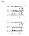
- FIG. 2 An image display apparatus 10 of FIG. 2 is supposed to be used for viewing images from the substrate 11 side as shown in the figure; however, the present invention is not intended to be limited by the structure in which images are viewed from the substrate 11 side. Moreover, since the apparatus is provided with no electrode 15 , the apparatus having a type indicated by FIG. 2( b ) can be simplified in its apparatus structure and is advantageous in that its manufacturing processes can be shortened.
- FIG. 4 shows a state in which the image display apparatus 10 of the type shown in FIG. 2( b ) is set in a device capable of applying a voltage so that the voltage is applied thereto. Additionally, the cross-sectional structure of the image display apparatus of the present invention is not intended to be limited by those shown in FIGS. 2( a ) and 2 ( b ).
- Electrodes 15 used for applying a voltage are provided on the respective surfaces of the substrates 11 and 12 on the mutually opposed sides, and insulating layers 16 are further formed on the respective electrodes 15 .
- the electrode 15 and the insulating layer 16 are provided on each of the substrates 11 and 12 , and display particles are located in a gap 18 that is formed by making the surfaces each having the electrode 15 and the insulating layer 16 face to face with each other.
- the image display apparatus 10 of FIG. 2 has two types of display particles, that is, black display particles 21 (hereinafter, referred to as “black particles”) and white display particles 22 (hereinafter, referred to as “white particles”), located in the gas 18 as display particles.
- the image display apparatus 10 of FIG. 2 has a structure in which the gap 18 is surrounded by the substrates 11 , and 12 and two barrier ribs 17 from four sides, with the display particles being sealed in the gap 18 .
- the thickness of the gap 18 is not particularly limited as long as it is kept in such a range as to allow the sealed display particles to move and properly maintain the contrast of an image, and is normally in a range from 10 ⁇ m to 500 ⁇ m, and preferably from 10 ⁇ m to 100 ⁇ m.
- the volume-filling-ratio of the display particles in the gap 18 is 5% to 70%, and preferably from 30% to 60%. By making the volume-filling-ratio of the display particles within the above-mentioned range, the display particles are allowed to move smoothly in the gap 18 , and an image with superior contrast can be obtained.
- the charging method of display particles by the above-mentioned known method for example, a method is proposed in which the display particles are made in contact with the carrier so as to be charged by frictional charging, and another method is proposed in which display particles of two colors having different charging polarities are mixed and stirred so that the display particles are charged by frictional charging among the particles of the two types.
- the carrier is used, and the charged display particles are preferably sealed between the substrates.
- FIGS. 3 and 4 show examples of movements of display particles in response to a voltage application between the substrates.
- FIG. 3( a ) shows a state prior to the voltage application between substrates 11 and 12 , and prior to the voltage application, white particles 22 positively charged are located near the substrate 11 on the visible side. This state shows that the image display apparatus 10 displays a white image.
- FIG. 3( b ) shows a state after the application of voltage to the electrode 15 in which the negatively charged black particles 21 have been moved close to the substrate 11 on the visible side by an application of a positive voltage to the substrate 11 , while the white particles 22 have been moved to the substrate 12 side. In this state, the image display apparatus 10 displays a black image.
- FIG. 4 show a structure in which the image display apparatus 10 shown in FIG. 2( b ) of a type without electrodes is connected to a voltage application device 30 , and also show a state prior to an application of a voltage in this state ( FIG. 4( a )) and a state after the application of the voltage ( FIG. 4( b )).
- the image display apparatus 10 having the electrode 15 the image display apparatus 10 of the type shown in FIG. 2( b ) also has a state in which the negatively charged black particles 21 have been moved close to the substrate 11 on the visible side by the application of a positive voltage to the substrate 11 , while the positively charged white particles 22 have been moved to the substrate 12 side.
- the thicknesses of the substrates 11 and 12 are preferably 2 ⁇ m to 5 mm, and more preferably 5 ⁇ m to 2 mm, respectively.
- the thicknesses of the substrates 11 and 12 are set within the above-mentioned range, it is possible to allow the image display apparatus 10 to have sufficient strength, with the gap between the substrates being maintained uniformly.
- a compact, light-weight image display apparatus can be provided so that the application of the image display apparatus can be promoted in a wider field.
- by making the thickness of the substrate on the image visible side within the above-mentioned range it is possible to provide accurate visual recognition of a displayed image and consequently to prevent problems with display quality.
- the material having a visible light transmittance of 80% or more examples thereof include an inorganic material, such as glass and quartz, having no flexibility, an organic material typically represented by a resin material, which will be described later, and a metal sheet.
- the organic material and the metal sheet allow the image display apparatus to have a certain degree of flexibility.
- the resin material capable of providing a visible light transmittance of 80% or more for example, polyester resins typically represented by polyethylene terephthalate and polyethylene naphthalate, polycarbonate resin, polyether sulfone resin, polyimide resin and the like may be used.
- the electrodes 15 are provided on the surfaces of the substrates 11 and 12 , and used for forming an electric field between the substrates, that is, in the gap 18 , by applying a voltage. In the same manner as in the aforementioned substrates, the electrode 15 to be formed on the image visible side to the viewer needs to be formed by using a transparent material.
- examples thereof include: a metal material and a conductive metal oxide, or a conductive polymer material.
- the metal material include: aluminum, silver, nickel, copper, gold and the like
- specific examples of the conductive metal oxide include: indium-tin oxide (ITO), indium oxide, antimony-tin oxide (ATO), tin oxide, zinc oxide and the like.
- examples of the conductive polymer material include: polyaniline, polypyrrole, polythiophene, polyacetylene, and the like.
- a sputtering method for example, in a case of forming a thin-film electrode, a sputtering method, a vacuum vapor deposition method, a chemical vapor deposition method (CVD method) and a coating method are proposed.
- CVD method chemical vapor deposition method
- a coating method for example, a conductive material is mixed in a solvent and a binder resin and this mixture is applied to a substrate so as to form an electrode.
- the insulating layer 16 is provided on the surface of the electrode 15 , and has such a structure that the surface of the insulating layer 16 is made in contact with the display particles 21 and 22 ; however, the insulating layer 16 is not necessarily required to be installed.
- the insulating layer 16 has a function for alleviating a change in quantity of charge due to a voltage applied upon moving the display particles 21 and 22 .
- the insulating layer makes it possible to reduce the physical adhesion force to the display particles, and consequently to reduce the driving voltage.
- the material for constituting the insulating layer 16 such a material that has an electrical insulating property, can be formed into a thin film, and also has a transparent property, if necessary, is preferably used.
- the insulating layer to be provided on the image visible side is preferably designed to have a visible light transmittance of 80% or more in the same manner as in the substrate. Specific examples thereof include: silicone resin, acrylic resin, polycarbonate resin, and the like.
- the thickness of the insulating layer 16 is preferably 0.01 ⁇ m or more to 10.0 ⁇ m or less. That is, when the thickness of the insulating layer 16 is within the above-mentioned range, it is possible to move the display particles 21 , 22 without applying a high voltage between the electrodes 15 , and this structure is preferable because, for example, an image displaying process can be carried out by applying a voltage in such a level as to be applied during an image forming process by the use of an electrophoretic method.
- the barrier rib 17 to be formed inside of the substrate 11 , 12 may be formed continuously, or may be formed intermittently, in a direction from the surface to rear face, in figures shown on the right side and left side in the upper stage of FIG. 5 .
- the cell of the gap 18 divided by the barrier ribs 17 can be arranged with various shapes. Examples of the shape and arrangement of the cells at the time when the gap 18 is viewed in the visually recognizable direction of the substrate 11 are shown in the lower stage of FIG. 5 . As shown in the lower stage of FIG. 5 , a plurality of cells with a square shape, a triangular shape, a line shape, a round shape, a hexagonal shape or the like can be arranged into a honeycomb shape and a network shape.
- the barrier ribs 17 can be formed by carrying out a shaping process on the substrate on the side opposite to the image-recognizing side, for example, by using the following method.
- a method for shaping the barrier ribs 17 for example, a method for forming irregularities by using an embossing process and a thermal press injection molding process to be carried out on a resin material or the like, a photolithography method, a screen printing method and the like are proposed.
- the image display apparatus can be manufactured by an electrophotographic developing system as described below.
- An electrode 15 and an insulating layer 16 are formed on each of two substrates 11 and 12 so that a pair of substrates with electrodes formed thereon are obtained.
- the display particles 21 are negatively charged, and the mixtures ( 21 , 210 ) are placed on a conductive stage 100 as shown in FIG. 6( a ), and one of the substrates with electrodes is placed with a predetermined gap being set from the stage 100 .
- a DC voltage having a positive polarity and an AC voltage are applied to the electrode 15 so that the negatively charged display particles 21 are allowed to adhere thereto.
- the display particles 22 are positively charged, and the mixtures ( 22 , 220 ) are placed on the conductive stage 100 , as shown in FIG. 6( b ), and the other substrate with electrodes is placed with a predetermined gap being set from the stage 100 .
- a DC voltage having a negative polarity and an AC voltage are applied to the electrode 15 so that the positively charged display particles 22 are allowed to adhere thereto.
- the substrate with electrodes to which the negatively charged display particles have been adhered and the substrate with electrodes to which the positively charged display particles have been adhered are superposed as shown in FIG. 6( c ) by adjusting the barrier ribs so as to form a predetermined gap, and the peripheral portions of the substrates are bonded so that an image display apparatus can be obtained.
- the carrier 210 used for negatively charging the display particles for example, a coat-type carrier formed by coating magnetic particles such as ferrite with a resin such as a cyclohexylmethacrylate resin is effectively used.
- the carrier 220 used for the positively charging display particles for example, a coat-type carrier formed by coating magnetic particles such as ferrite with a resin such as a fluoridated acrylate resin is effectively used.
- the following resin and carbon black were loaded into a Henschel mixer (made by Mitsui-Miike Machinery Co., Ltd.) and a peripheral speed of stirring blades was set to 25 m/s so that a mixing process was carried out for five minutes to provide a mixture.
- Styrene acrylic resin (weight average molecular weight 20,000) 100 parts by weight
- the above-mentioned mixture was kneaded by a twin-screw extrusion kneader, coarsely pulverized by a hummer mill, then subjected to a grinding process by a turbo-mill grinder (made by Turbo Kogyo Co., Ltd.), and further subjected to a fine-particle classifying process by a gas-flow classifier utilizing a Coanda effect so that black base particles having a volume-average particle size of 8.2 ⁇ m were produced.
- the black base particles (30 g) were dispersed in 1000 g of pure water, and 10 g of ammonia water (28 wt %) was added thereto, and this was stirred for 5 minutes. Next, tetraethoxysilane (8.5 g) and dimethyldiethoxysilane (8.5 g) were dropped thereto in 3 hours, and this was stirred for 5 hours at room temperature. The resulting precipitate was filtrated, and after having been washed with pure water, this was dried at 60° C. for 24 hours so that black display particles in which a silica fine particle layer was formed on the surface of each of the black base particles were obtained.
- the black display particles (10 g) in which the metal oxide layers were formed were added to a mixed solution of 50 g of cyclohexane and 10 g of hexamethyldisilazane, and this dispersion solution was heated to 50° C., while being stirred, so as to react with each other for 3 hours. Next, the solvent in this dispersion solution was distilled off at 50° C. under a reduced pressure so that black display particles were obtained.
- the following resin and titanium oxide were loaded into a Henschel mixer (made by Mitsui-Miike machinery Co., Ltd.) and a peripheral speed of stirring blades was set to 25 m/s so that a mixing process was carried out for five minutes to provide a mixture.
- Styrene acrylic resin (weight average molecular weight 20,000) 100 parts by weight
- Rutile type titanium dioxide (R-630: made by Ishihara Sangyo Co., Ltd.) 100 parts by weight
- the above-mentioned mixture was kneaded by a twin-screw extrusion kneader, coarsely pulverized by a hummer mill, then subjected to a grinding process by a turbo-mill grinder (made by Turbo Kogyo Co., Ltd.), and further subjected to a fine-particle classifying process by a gas-flow classifier utilizing a Coanda effect so that white base particles having a volume-average particle size of 8.0 ⁇ m were produced.
- the white base particles (30 g) were dispersed in 1000 g of pure water, and 10 g of ammonia water (28 wt %) was added thereto, and this was stirred for 5 minutes. Next, tetraethoxysilane (8.5 g) and dimethyldiethoxysilane (8.5 g) were dropped thereto in 3 hours, and this was stirred for 5 hours at room temperature. The resulting precipitate was filtrated, and after having been washed with pure water, this was dried at 60° C. for 24 hours so that white display particles in which a silica fine particle layer was formed on the surface of each of the white base particles were obtained.
- the resulting white particles were added to a mixed solution of 50 g of cyclohexane and 10 g of hexamethyldisilazane (second processing agent), and this was heated at 50° C., while being stirred, so as to react with each other for 3 hours.
- the solvent in this dispersion solution was distilled off at 50° C. under a reduced pressure so that white display particles were obtained.
- ferrite cores having an average particle size of 80 ⁇ m were added 2 parts of cyclohexylmethacrylate resin particles, and these materials were put into a horizontal rotation blade type mixer, and mixed and stirred at 22° C. for 10 minutes under a condition of 8 m/sec in the peripheral speed of the horizontal rotation blades. The resulting mixture was then heated to 90° C., and stirred for 40 minutes so that carrier B was prepared.
- An image display apparatus was manufactured in accordance with the following method so as to have the same structure as that of FIG. 2( a ).
- Two sheets of glass substrates 11 each having a length of 80 mm, a width of 50 mm and a thickness of 0.7 mm were prepared, and an electrode 15 made of an indium-tin oxide (ITO) film (resistance: 30 ⁇ / ⁇ ) having a thickness of 300 nm was formed on each of the substrate surfaces by using a vapor deposition method.
- ITO indium-tin oxide
- a coating solution prepared by dissolving 12 g of a polycarbonate resin in a mixed solvent of 80 ml of tetrahydrofuran and 20 ml of cyclohexanone was applied by using a spin coating method so that an insulating layer 16 having a thickness of 3 ⁇ m was formed; thus, a pair of substrates with electrodes formed thereon was obtained.
- Black display particles (1 g) and carrier B (9 g) were mixed by a shaker (YS-LD, made by Yayoi Co., Ltd.) for 30 minutes so that display particles were charged.
- the resulting mixtures ( 21 , 210 ) were put on a conductive stage 100 , as shown in FIG. 6( a ), and one of the substrates with electrodes was disposed with a gap of about 2 mm being set from the stage 100 .
- a DC bias of +50V and an AC bias of 2.0 kV were applied with a frequency of 2.0 kHz for 10 seconds so that black display particles 21 were allowed to adhere onto the insulating layer 16 .
- White display particles (1 g) and carrier A (9 g) were mixed by a shaker (YS-LD, made by Yayoi Co., Ltd.) for 30 minutes so that the display particles were charged.
- the resulting mixtures ( 22 , 220 ) were put on a conductive stage 100 , as shown in FIG. 6( b ), and the other substrate with electrodes was disposed with a gap of about 2 mm being maintained from the stage 100 .
- a DC bias of ⁇ 50V and an AC bias of 2.0 kV were applied with a frequency of 2.0 kHz for 10 seconds so that the white display particles 22 were allowed to adhere onto the insulating layer 16 .
- the substrate with electrodes to which the black display particles were adhered and the substrate with electrodes to which the white display particles were adhered were superposed so as to have a gap of 50 ⁇ m by making adjustments by barrier ribs, and the peripheral portions of the substrates were bonded to each other with an epoxy-based adhesive so that an image display apparatus was prepared. Additionally, the volume-filling-ratio of the two display particles between glass substrates was 50%. The mixing rate of the white display particles and the black display particles was set to 1/1 in weight ratio.
- An image display apparatus was manufactured by using the same method as that of example 1, except that, upon producing the white display particles and black display particles, predetermined compound A and compound B shown in Tables 1 and 2 were applied at a predetermined ratio.
- a DC voltage was applied to the image display apparatus in the following processes, and by measuring the reflection density of a display image obtained by the voltage application, the display characteristic was evaluated. Additionally, the voltage application was carried out by the following processes: that is, the voltage is applied in a manner so as to follow a hysteresis curve of a course in which, after the applied voltage has been changed from 0V to the plus side, it is successively changed to the minus side, and then returned to 0V.
- the black color density was a reflection density of the display surface obtained upon application of a voltage of +100 V to the electrode on the upstream side in the visually recognizable direction of the image display apparatus.
- the white color density was a reflection density of the display surface obtained upon application of a voltage of ⁇ 100 V to the electrode on the upstream side in the visually recognizable direction of the image display apparatus.
- the repetitive characteristic was evaluated in the following manner: voltage applications of +100 V and ⁇ 100 V were alternately repeated, and at the time when, upon measuring the reflection density each time, the contrast became 0.70 or less, the repetitive characteristic was evaluated based upon the number of repetition times at this time.
- the repetitive characteristic was evaluated based upon the following criteria: the repetition times of 50000 or more was rated as superior ( ⁇ ); the repetition times of 30000 or more was rated as acceptable ( ⁇ ) and the repetition times of less than 30000 was rated as rejected ( ⁇ ).
- the metal oxide layers comprise a polycondensation product formed by predetermined compounds and the flexibility of the metal oxide layers are thus improved, it is possible to prevent cracks and film separations from occurring in the metal oxide layers for a long period of time. As a result, it becomes possible to sufficiently prevent degradation of contrast during repetitive driving operations for a long period of time.
Landscapes
- Physics & Mathematics (AREA)
- Nonlinear Science (AREA)
- Health & Medical Sciences (AREA)
- Life Sciences & Earth Sciences (AREA)
- Chemical & Material Sciences (AREA)
- Chemical Kinetics & Catalysis (AREA)
- Electrochemistry (AREA)
- Molecular Biology (AREA)
- General Physics & Mathematics (AREA)
- Optics & Photonics (AREA)
- Electrochromic Elements, Electrophoresis, Or Variable Reflection Or Absorption Elements (AREA)
Applications Claiming Priority (3)
| Application Number | Priority Date | Filing Date | Title |
|---|---|---|---|
| JP2009-145421 | 2009-06-18 | ||
| JP2009145421 | 2009-06-18 | ||
| JP2009145421A JP2011002644A (ja) | 2009-06-18 | 2009-06-18 | 画像表示装置用表示粒子および画像表示装置 |
Publications (2)
| Publication Number | Publication Date |
|---|---|
| US20100321762A1 US20100321762A1 (en) | 2010-12-23 |
| US8248685B2 true US8248685B2 (en) | 2012-08-21 |
Family
ID=43354111
Family Applications (1)
| Application Number | Title | Priority Date | Filing Date |
|---|---|---|---|
| US12/814,556 Expired - Fee Related US8248685B2 (en) | 2009-06-18 | 2010-06-14 | Display particles for image display apparatus and image display apparatus loaded with the same |
Country Status (2)
| Country | Link |
|---|---|
| US (1) | US8248685B2 (OSRAM) |
| JP (1) | JP2011002644A (OSRAM) |
Cited By (1)
| Publication number | Priority date | Publication date | Assignee | Title |
|---|---|---|---|---|
| US20100302622A1 (en) * | 2008-09-12 | 2010-12-02 | Konica Minolta Business Technologies, Inc. | Display particles for image display device and image display device installed with the same |
Families Citing this family (5)
| Publication number | Priority date | Publication date | Assignee | Title |
|---|---|---|---|---|
| US8557877B2 (en) * | 2009-06-10 | 2013-10-15 | Honeywell International Inc. | Anti-reflective coatings for optically transparent substrates |
| US9335443B2 (en) | 2011-04-15 | 2016-05-10 | Qspex Technologies, Inc. | Anti-reflective lenses and methods for manufacturing the same |
| US8864898B2 (en) | 2011-05-31 | 2014-10-21 | Honeywell International Inc. | Coating formulations for optical elements |
| JP5942394B2 (ja) * | 2011-11-22 | 2016-06-29 | ソニー株式会社 | 電気泳動素子および表示装置 |
| AU2012392166B2 (en) * | 2012-10-10 | 2015-10-29 | Qspex Technologies, Inc. | Anti-reflective lenses and methods for manufacturing the same |
Citations (5)
| Publication number | Priority date | Publication date | Assignee | Title |
|---|---|---|---|---|
| JP2003167277A (ja) | 2001-09-19 | 2003-06-13 | Bridgestone Corp | 画像表示用粒子および画像表示装置 |
| JP2004029699A (ja) | 2002-05-02 | 2004-01-29 | Bridgestone Corp | 画像表示用粒子及びそれを用いた画像表示装置 |
| JP2006072345A (ja) | 2004-08-05 | 2006-03-16 | Bridgestone Corp | 表示媒体用粒子及びそれを利用した情報表示用パネル |
| US20090251764A1 (en) * | 2008-04-02 | 2009-10-08 | Konica Minolta Business Technologies, Inc. | Image display device |
| US20100208330A1 (en) * | 2009-02-16 | 2010-08-19 | Konica Minolta Business Technologies, Inc. | Image display apparatus |
Family Cites Families (8)
| Publication number | Priority date | Publication date | Assignee | Title |
|---|---|---|---|---|
| JPS5028446B2 (OSRAM) * | 1971-11-19 | 1975-09-16 | ||
| JPS62275170A (ja) * | 1986-05-23 | 1987-11-30 | Matsushita Electric Works Ltd | コ−テイング材の製法 |
| JPH08185619A (ja) * | 1994-12-28 | 1996-07-16 | Fuji Photo Film Co Ltd | 磁気記録媒体およびその製造方法 |
| JP4049131B2 (ja) * | 2004-07-07 | 2008-02-20 | 株式会社デンソー | 車両用ナビゲーション装置 |
| JP2006106596A (ja) * | 2004-10-08 | 2006-04-20 | Bridgestone Corp | 情報表示用パネルに用いる表示媒体用粒子 |
| JP2006162723A (ja) * | 2004-12-03 | 2006-06-22 | Chisso Corp | ケイ素含有微粒子及びそれを含む電気泳動型表示素子 |
| JP2007169507A (ja) * | 2005-12-22 | 2007-07-05 | Chisso Corp | アンモニウムシラン変性ケイ素含有微粒子、電気泳動表示装置用表示液及びそれを含む電気泳動型表示素子 |
| CN101489947B (zh) * | 2006-09-08 | 2014-07-30 | 中央硝子株式会社 | 车辆用热射线屏蔽玻璃及其生产方法 |
-
2009
- 2009-06-18 JP JP2009145421A patent/JP2011002644A/ja active Pending
-
2010
- 2010-06-14 US US12/814,556 patent/US8248685B2/en not_active Expired - Fee Related
Patent Citations (5)
| Publication number | Priority date | Publication date | Assignee | Title |
|---|---|---|---|---|
| JP2003167277A (ja) | 2001-09-19 | 2003-06-13 | Bridgestone Corp | 画像表示用粒子および画像表示装置 |
| JP2004029699A (ja) | 2002-05-02 | 2004-01-29 | Bridgestone Corp | 画像表示用粒子及びそれを用いた画像表示装置 |
| JP2006072345A (ja) | 2004-08-05 | 2006-03-16 | Bridgestone Corp | 表示媒体用粒子及びそれを利用した情報表示用パネル |
| US20090251764A1 (en) * | 2008-04-02 | 2009-10-08 | Konica Minolta Business Technologies, Inc. | Image display device |
| US20100208330A1 (en) * | 2009-02-16 | 2010-08-19 | Konica Minolta Business Technologies, Inc. | Image display apparatus |
Cited By (1)
| Publication number | Priority date | Publication date | Assignee | Title |
|---|---|---|---|---|
| US20100302622A1 (en) * | 2008-09-12 | 2010-12-02 | Konica Minolta Business Technologies, Inc. | Display particles for image display device and image display device installed with the same |
Also Published As
| Publication number | Publication date |
|---|---|
| JP2011002644A (ja) | 2011-01-06 |
| US20100321762A1 (en) | 2010-12-23 |
Similar Documents
| Publication | Publication Date | Title |
|---|---|---|
| US20090242847A1 (en) | Display particles for image display apparatus and image display apparatus | |
| US8248685B2 (en) | Display particles for image display apparatus and image display apparatus loaded with the same | |
| JP2009086135A (ja) | 画像表示装置 | |
| US7830593B2 (en) | Image display device | |
| US20100207868A1 (en) | Display particles for image display apparatus and image display apparatus using the same | |
| US7952794B2 (en) | Image display apparatus | |
| US7903323B2 (en) | Image display apparatus | |
| JP2010091908A (ja) | 画像表示装置 | |
| JP5396875B2 (ja) | 画像表示装置用表示粒子および画像表示装置 | |
| US7839562B2 (en) | White particles for image display device | |
| JP2010048861A (ja) | 画像表示媒体 | |
| US20100302622A1 (en) | Display particles for image display device and image display device installed with the same | |
| JP4945099B2 (ja) | 表示媒体用粒子及びそれを利用した情報表示用パネル | |
| US7969643B2 (en) | Display particles for image display apparatus and image display apparatus loaded with the same | |
| CN100357819C (zh) | 图像显示介质中使用的粒子、使用该粒子的图像显示用平板及图像显示装置 | |
| JP2010282012A (ja) | 画像表示装置用表示粒子および画像表示装置 | |
| JP5131042B2 (ja) | 画像表示装置 | |
| JP5228638B2 (ja) | 画像表示装置用表示粒子および画像表示装置 | |
| JP5298920B2 (ja) | 画像表示装置用表示粒子および画像表示装置 | |
| JP5381036B2 (ja) | 白色表示粒子および画像表示装置 | |
| JP4501393B2 (ja) | 表示デバイス用粒子、画像表示媒体および画像形成装置 | |
| JP5315962B2 (ja) | 画像表示装置用表示粒子および画像表示装置 | |
| JP2010026451A (ja) | 画像表示装置用表示粒子および画像表示装置 | |
| JP2010128075A (ja) | 画像表示装置用表示粒子および画像表示装置 | |
| JP2009216879A (ja) | 画像表示装置用表示粒子および画像表示装置 |
Legal Events
| Date | Code | Title | Description |
|---|---|---|---|
| AS | Assignment |
Owner name: KONICA MINOLTA BUSINESS TECHNOLOGIES, INC., JAPAN Free format text: ASSIGNMENT OF ASSIGNORS INTEREST;ASSIGNORS:SHIBATA, KOUJI;OKUYAMA, OKUSHI;HOSOYA, YUKIO;AND OTHERS;REEL/FRAME:024528/0192 Effective date: 20100513 |
|
| FEPP | Fee payment procedure |
Free format text: PAYOR NUMBER ASSIGNED (ORIGINAL EVENT CODE: ASPN); ENTITY STATUS OF PATENT OWNER: LARGE ENTITY |
|
| STCF | Information on status: patent grant |
Free format text: PATENTED CASE |
|
| FPAY | Fee payment |
Year of fee payment: 4 |
|
| FEPP | Fee payment procedure |
Free format text: MAINTENANCE FEE REMINDER MAILED (ORIGINAL EVENT CODE: REM.); ENTITY STATUS OF PATENT OWNER: LARGE ENTITY |
|
| LAPS | Lapse for failure to pay maintenance fees |
Free format text: PATENT EXPIRED FOR FAILURE TO PAY MAINTENANCE FEES (ORIGINAL EVENT CODE: EXP.); ENTITY STATUS OF PATENT OWNER: LARGE ENTITY |
|
| STCH | Information on status: patent discontinuation |
Free format text: PATENT EXPIRED DUE TO NONPAYMENT OF MAINTENANCE FEES UNDER 37 CFR 1.362 |
|
| FP | Lapsed due to failure to pay maintenance fee |
Effective date: 20200821 |