US8101507B2 - Semiconductor device manufacturing method and semiconductor device manufacturing apparatus - Google Patents
Semiconductor device manufacturing method and semiconductor device manufacturing apparatus Download PDFInfo
- Publication number
- US8101507B2 US8101507B2 US12/580,495 US58049509A US8101507B2 US 8101507 B2 US8101507 B2 US 8101507B2 US 58049509 A US58049509 A US 58049509A US 8101507 B2 US8101507 B2 US 8101507B2
- Authority
- US
- United States
- Prior art keywords
- insulating film
- etching
- low dielectric
- plasma
- wafer
- Prior art date
- Legal status (The legal status is an assumption and is not a legal conclusion. Google has not performed a legal analysis and makes no representation as to the accuracy of the status listed.)
- Expired - Fee Related, expires
Links
- 239000004065 semiconductor Substances 0.000 title claims abstract description 51
- 238000004519 manufacturing process Methods 0.000 title claims abstract description 47
- 238000000034 method Methods 0.000 claims abstract description 301
- 230000008569 process Effects 0.000 claims abstract description 293
- 238000005530 etching Methods 0.000 claims abstract description 103
- 230000001678 irradiating effect Effects 0.000 claims abstract description 14
- 239000000758 substrate Substances 0.000 claims abstract description 14
- 238000006884 silylation reaction Methods 0.000 claims description 77
- 238000004380 ashing Methods 0.000 claims description 56
- 239000002184 metal Substances 0.000 claims description 17
- 229910052751 metal Inorganic materials 0.000 claims description 17
- 238000004140 cleaning Methods 0.000 claims description 14
- 229920002120 photoresistant polymer Polymers 0.000 claims description 8
- 238000011049 filling Methods 0.000 claims description 5
- 238000009413 insulation Methods 0.000 claims description 4
- 230000010287 polarization Effects 0.000 claims description 3
- 235000012431 wafers Nutrition 0.000 description 109
- 238000012545 processing Methods 0.000 description 60
- 238000012546 transfer Methods 0.000 description 32
- 239000011229 interlayer Substances 0.000 description 29
- 230000007246 mechanism Effects 0.000 description 21
- IJGRMHOSHXDMSA-UHFFFAOYSA-N Atomic nitrogen Chemical compound N#N IJGRMHOSHXDMSA-UHFFFAOYSA-N 0.000 description 20
- 229910001873 dinitrogen Inorganic materials 0.000 description 20
- 239000010410 layer Substances 0.000 description 20
- KAHVZNKZQFSBFW-UHFFFAOYSA-N n-methyl-n-trimethylsilylmethanamine Chemical compound CN(C)[Si](C)(C)C KAHVZNKZQFSBFW-UHFFFAOYSA-N 0.000 description 18
- 239000012298 atmosphere Substances 0.000 description 16
- 238000011068 loading method Methods 0.000 description 15
- 239000010949 copper Substances 0.000 description 11
- 229910052731 fluorine Inorganic materials 0.000 description 11
- 239000007789 gas Substances 0.000 description 11
- XLYOFNOQVPJJNP-UHFFFAOYSA-N water Substances O XLYOFNOQVPJJNP-UHFFFAOYSA-N 0.000 description 11
- YCKRFDGAMUMZLT-UHFFFAOYSA-N Fluorine atom Chemical compound [F] YCKRFDGAMUMZLT-UHFFFAOYSA-N 0.000 description 10
- 239000011737 fluorine Substances 0.000 description 10
- 239000003795 chemical substances by application Substances 0.000 description 9
- 238000005259 measurement Methods 0.000 description 9
- 229910052760 oxygen Inorganic materials 0.000 description 9
- QVGXLLKOCUKJST-UHFFFAOYSA-N atomic oxygen Chemical compound [O] QVGXLLKOCUKJST-UHFFFAOYSA-N 0.000 description 8
- 238000010586 diagram Methods 0.000 description 8
- 239000001301 oxygen Substances 0.000 description 8
- 125000002496 methyl group Chemical group [H]C([H])([H])* 0.000 description 7
- 230000004888 barrier function Effects 0.000 description 6
- 239000000969 carrier Substances 0.000 description 6
- 230000008859 change Effects 0.000 description 6
- 238000010438 heat treatment Methods 0.000 description 6
- 229920000642 polymer Polymers 0.000 description 6
- VYPSYNLAJGMNEJ-UHFFFAOYSA-N Silicium dioxide Chemical compound O=[Si]=O VYPSYNLAJGMNEJ-UHFFFAOYSA-N 0.000 description 5
- 238000006243 chemical reaction Methods 0.000 description 5
- 230000001681 protective effect Effects 0.000 description 5
- 229910008284 Si—F Inorganic materials 0.000 description 4
- 238000010521 absorption reaction Methods 0.000 description 4
- 229910052799 carbon Inorganic materials 0.000 description 4
- 230000007423 decrease Effects 0.000 description 4
- 238000001020 plasma etching Methods 0.000 description 4
- 238000011084 recovery Methods 0.000 description 4
- 239000006200 vaporizer Substances 0.000 description 4
- OKTJSMMVPCPJKN-UHFFFAOYSA-N Carbon Chemical compound [C] OKTJSMMVPCPJKN-UHFFFAOYSA-N 0.000 description 3
- RYGMFSIKBFXOCR-UHFFFAOYSA-N Copper Chemical compound [Cu] RYGMFSIKBFXOCR-UHFFFAOYSA-N 0.000 description 3
- 229910008051 Si-OH Inorganic materials 0.000 description 3
- 229910002808 Si–O–Si Inorganic materials 0.000 description 3
- 229910006358 Si—OH Inorganic materials 0.000 description 3
- 238000004458 analytical method Methods 0.000 description 3
- 238000000137 annealing Methods 0.000 description 3
- 238000006482 condensation reaction Methods 0.000 description 3
- 229910052802 copper Inorganic materials 0.000 description 3
- 230000006866 deterioration Effects 0.000 description 3
- 238000011161 development Methods 0.000 description 3
- 230000009977 dual effect Effects 0.000 description 3
- 238000009713 electroplating Methods 0.000 description 3
- 239000007788 liquid Substances 0.000 description 3
- KRHYYFGTRYWZRS-UHFFFAOYSA-N Fluorane Chemical compound F KRHYYFGTRYWZRS-UHFFFAOYSA-N 0.000 description 2
- 238000005033 Fourier transform infrared spectroscopy Methods 0.000 description 2
- 229910020175 SiOH Inorganic materials 0.000 description 2
- XUIMIQQOPSSXEZ-UHFFFAOYSA-N Silicon Chemical compound [Si] XUIMIQQOPSSXEZ-UHFFFAOYSA-N 0.000 description 2
- 230000015556 catabolic process Effects 0.000 description 2
- 229910052681 coesite Inorganic materials 0.000 description 2
- 229910052906 cristobalite Inorganic materials 0.000 description 2
- 238000006731 degradation reaction Methods 0.000 description 2
- 238000003795 desorption Methods 0.000 description 2
- 230000005684 electric field Effects 0.000 description 2
- 230000002209 hydrophobic effect Effects 0.000 description 2
- 125000002887 hydroxy group Chemical group [H]O* 0.000 description 2
- 230000006872 improvement Effects 0.000 description 2
- 230000033001 locomotion Effects 0.000 description 2
- 238000004949 mass spectrometry Methods 0.000 description 2
- 239000007769 metal material Substances 0.000 description 2
- 238000012986 modification Methods 0.000 description 2
- 230000004048 modification Effects 0.000 description 2
- 230000003647 oxidation Effects 0.000 description 2
- 238000007254 oxidation reaction Methods 0.000 description 2
- 230000001590 oxidative effect Effects 0.000 description 2
- 230000003071 parasitic effect Effects 0.000 description 2
- 229910052710 silicon Inorganic materials 0.000 description 2
- 239000010703 silicon Substances 0.000 description 2
- 239000000377 silicon dioxide Substances 0.000 description 2
- 229910052682 stishovite Inorganic materials 0.000 description 2
- 229910052905 tridymite Inorganic materials 0.000 description 2
- 229910052782 aluminium Inorganic materials 0.000 description 1
- XAGFODPZIPBFFR-UHFFFAOYSA-N aluminium Chemical compound [Al] XAGFODPZIPBFFR-UHFFFAOYSA-N 0.000 description 1
- 230000015572 biosynthetic process Effects 0.000 description 1
- 238000001311 chemical methods and process Methods 0.000 description 1
- 239000011248 coating agent Substances 0.000 description 1
- 238000000576 coating method Methods 0.000 description 1
- 238000011109 contamination Methods 0.000 description 1
- 238000007796 conventional method Methods 0.000 description 1
- 230000003247 decreasing effect Effects 0.000 description 1
- 230000007547 defect Effects 0.000 description 1
- 238000009792 diffusion process Methods 0.000 description 1
- KPUWHANPEXNPJT-UHFFFAOYSA-N disiloxane Chemical group [SiH3]O[SiH3] KPUWHANPEXNPJT-UHFFFAOYSA-N 0.000 description 1
- 238000002474 experimental method Methods 0.000 description 1
- 239000001257 hydrogen Substances 0.000 description 1
- 229910052739 hydrogen Inorganic materials 0.000 description 1
- 125000004435 hydrogen atom Chemical class [H]* 0.000 description 1
- 230000007257 malfunction Effects 0.000 description 1
- 239000000203 mixture Substances 0.000 description 1
- 238000007747 plating Methods 0.000 description 1
- 238000010926 purge Methods 0.000 description 1
- 238000009877 rendering Methods 0.000 description 1
- LIVNPJMFVYWSIS-UHFFFAOYSA-N silicon monoxide Chemical compound [Si-]#[O+] LIVNPJMFVYWSIS-UHFFFAOYSA-N 0.000 description 1
- 229910052814 silicon oxide Inorganic materials 0.000 description 1
- 238000004528 spin coating Methods 0.000 description 1
- 238000004544 sputter deposition Methods 0.000 description 1
- 239000000126 substance Substances 0.000 description 1
- 230000001629 suppression Effects 0.000 description 1
- 238000009281 ultraviolet germicidal irradiation Methods 0.000 description 1
- 238000005406 washing Methods 0.000 description 1
Images


Classifications
-
- H—ELECTRICITY
- H01—ELECTRIC ELEMENTS
- H01L—SEMICONDUCTOR DEVICES NOT COVERED BY CLASS H10
- H01L21/00—Processes or apparatus adapted for the manufacture or treatment of semiconductor or solid state devices or of parts thereof
- H01L21/02—Manufacture or treatment of semiconductor devices or of parts thereof
- H01L21/04—Manufacture or treatment of semiconductor devices or of parts thereof the devices having potential barriers, e.g. a PN junction, depletion layer or carrier concentration layer
- H01L21/18—Manufacture or treatment of semiconductor devices or of parts thereof the devices having potential barriers, e.g. a PN junction, depletion layer or carrier concentration layer the devices having semiconductor bodies comprising elements of Group IV of the Periodic Table or AIIIBV compounds with or without impurities, e.g. doping materials
- H01L21/30—Treatment of semiconductor bodies using processes or apparatus not provided for in groups H01L21/20 - H01L21/26
- H01L21/302—Treatment of semiconductor bodies using processes or apparatus not provided for in groups H01L21/20 - H01L21/26 to change their surface-physical characteristics or shape, e.g. etching, polishing, cutting
- H01L21/306—Chemical or electrical treatment, e.g. electrolytic etching
- H01L21/3065—Plasma etching; Reactive-ion etching
-
- H—ELECTRICITY
- H01—ELECTRIC ELEMENTS
- H01L—SEMICONDUCTOR DEVICES NOT COVERED BY CLASS H10
- H01L21/00—Processes or apparatus adapted for the manufacture or treatment of semiconductor or solid state devices or of parts thereof
- H01L21/02—Manufacture or treatment of semiconductor devices or of parts thereof
- H01L21/04—Manufacture or treatment of semiconductor devices or of parts thereof the devices having potential barriers, e.g. a PN junction, depletion layer or carrier concentration layer
- H01L21/18—Manufacture or treatment of semiconductor devices or of parts thereof the devices having potential barriers, e.g. a PN junction, depletion layer or carrier concentration layer the devices having semiconductor bodies comprising elements of Group IV of the Periodic Table or AIIIBV compounds with or without impurities, e.g. doping materials
- H01L21/30—Treatment of semiconductor bodies using processes or apparatus not provided for in groups H01L21/20 - H01L21/26
- H01L21/31—Treatment of semiconductor bodies using processes or apparatus not provided for in groups H01L21/20 - H01L21/26 to form insulating layers thereon, e.g. for masking or by using photolithographic techniques; After treatment of these layers; Selection of materials for these layers
- H01L21/3105—After-treatment
- H01L21/31058—After-treatment of organic layers
-
- H—ELECTRICITY
- H01—ELECTRIC ELEMENTS
- H01L—SEMICONDUCTOR DEVICES NOT COVERED BY CLASS H10
- H01L21/00—Processes or apparatus adapted for the manufacture or treatment of semiconductor or solid state devices or of parts thereof
- H01L21/02—Manufacture or treatment of semiconductor devices or of parts thereof
- H01L21/04—Manufacture or treatment of semiconductor devices or of parts thereof the devices having potential barriers, e.g. a PN junction, depletion layer or carrier concentration layer
- H01L21/18—Manufacture or treatment of semiconductor devices or of parts thereof the devices having potential barriers, e.g. a PN junction, depletion layer or carrier concentration layer the devices having semiconductor bodies comprising elements of Group IV of the Periodic Table or AIIIBV compounds with or without impurities, e.g. doping materials
- H01L21/30—Treatment of semiconductor bodies using processes or apparatus not provided for in groups H01L21/20 - H01L21/26
- H01L21/31—Treatment of semiconductor bodies using processes or apparatus not provided for in groups H01L21/20 - H01L21/26 to form insulating layers thereon, e.g. for masking or by using photolithographic techniques; After treatment of these layers; Selection of materials for these layers
- H01L21/3105—After-treatment
-
- H—ELECTRICITY
- H01—ELECTRIC ELEMENTS
- H01L—SEMICONDUCTOR DEVICES NOT COVERED BY CLASS H10
- H01L21/00—Processes or apparatus adapted for the manufacture or treatment of semiconductor or solid state devices or of parts thereof
- H01L21/70—Manufacture or treatment of devices consisting of a plurality of solid state components formed in or on a common substrate or of parts thereof; Manufacture of integrated circuit devices or of parts thereof
- H01L21/71—Manufacture of specific parts of devices defined in group H01L21/70
- H01L21/768—Applying interconnections to be used for carrying current between separate components within a device comprising conductors and dielectrics
- H01L21/76801—Applying interconnections to be used for carrying current between separate components within a device comprising conductors and dielectrics characterised by the formation and the after-treatment of the dielectrics, e.g. smoothing
- H01L21/76802—Applying interconnections to be used for carrying current between separate components within a device comprising conductors and dielectrics characterised by the formation and the after-treatment of the dielectrics, e.g. smoothing by forming openings in dielectrics
- H01L21/76807—Applying interconnections to be used for carrying current between separate components within a device comprising conductors and dielectrics characterised by the formation and the after-treatment of the dielectrics, e.g. smoothing by forming openings in dielectrics for dual damascene structures
- H01L21/76808—Applying interconnections to be used for carrying current between separate components within a device comprising conductors and dielectrics characterised by the formation and the after-treatment of the dielectrics, e.g. smoothing by forming openings in dielectrics for dual damascene structures involving intermediate temporary filling with material
-
- H—ELECTRICITY
- H01—ELECTRIC ELEMENTS
- H01L—SEMICONDUCTOR DEVICES NOT COVERED BY CLASS H10
- H01L21/00—Processes or apparatus adapted for the manufacture or treatment of semiconductor or solid state devices or of parts thereof
- H01L21/70—Manufacture or treatment of devices consisting of a plurality of solid state components formed in or on a common substrate or of parts thereof; Manufacture of integrated circuit devices or of parts thereof
- H01L21/71—Manufacture of specific parts of devices defined in group H01L21/70
- H01L21/768—Applying interconnections to be used for carrying current between separate components within a device comprising conductors and dielectrics
- H01L21/76801—Applying interconnections to be used for carrying current between separate components within a device comprising conductors and dielectrics characterised by the formation and the after-treatment of the dielectrics, e.g. smoothing
- H01L21/76802—Applying interconnections to be used for carrying current between separate components within a device comprising conductors and dielectrics characterised by the formation and the after-treatment of the dielectrics, e.g. smoothing by forming openings in dielectrics
- H01L21/76814—Applying interconnections to be used for carrying current between separate components within a device comprising conductors and dielectrics characterised by the formation and the after-treatment of the dielectrics, e.g. smoothing by forming openings in dielectrics post-treatment or after-treatment, e.g. cleaning or removal of oxides on underlying conductors
-
- H—ELECTRICITY
- H01—ELECTRIC ELEMENTS
- H01L—SEMICONDUCTOR DEVICES NOT COVERED BY CLASS H10
- H01L21/00—Processes or apparatus adapted for the manufacture or treatment of semiconductor or solid state devices or of parts thereof
- H01L21/70—Manufacture or treatment of devices consisting of a plurality of solid state components formed in or on a common substrate or of parts thereof; Manufacture of integrated circuit devices or of parts thereof
- H01L21/71—Manufacture of specific parts of devices defined in group H01L21/70
- H01L21/768—Applying interconnections to be used for carrying current between separate components within a device comprising conductors and dielectrics
- H01L21/76801—Applying interconnections to be used for carrying current between separate components within a device comprising conductors and dielectrics characterised by the formation and the after-treatment of the dielectrics, e.g. smoothing
- H01L21/76822—Modification of the material of dielectric layers, e.g. grading, after-treatment to improve the stability of the layers, to increase their density etc.
- H01L21/76825—Modification of the material of dielectric layers, e.g. grading, after-treatment to improve the stability of the layers, to increase their density etc. by exposing the layer to particle radiation, e.g. ion implantation, irradiation with UV light or electrons etc.
-
- H—ELECTRICITY
- H01—ELECTRIC ELEMENTS
- H01L—SEMICONDUCTOR DEVICES NOT COVERED BY CLASS H10
- H01L21/00—Processes or apparatus adapted for the manufacture or treatment of semiconductor or solid state devices or of parts thereof
- H01L21/70—Manufacture or treatment of devices consisting of a plurality of solid state components formed in or on a common substrate or of parts thereof; Manufacture of integrated circuit devices or of parts thereof
- H01L21/71—Manufacture of specific parts of devices defined in group H01L21/70
- H01L21/768—Applying interconnections to be used for carrying current between separate components within a device comprising conductors and dielectrics
- H01L21/76801—Applying interconnections to be used for carrying current between separate components within a device comprising conductors and dielectrics characterised by the formation and the after-treatment of the dielectrics, e.g. smoothing
- H01L21/76822—Modification of the material of dielectric layers, e.g. grading, after-treatment to improve the stability of the layers, to increase their density etc.
- H01L21/76826—Modification of the material of dielectric layers, e.g. grading, after-treatment to improve the stability of the layers, to increase their density etc. by contacting the layer with gases, liquids or plasmas
-
- H—ELECTRICITY
- H01—ELECTRIC ELEMENTS
- H01L—SEMICONDUCTOR DEVICES NOT COVERED BY CLASS H10
- H01L21/00—Processes or apparatus adapted for the manufacture or treatment of semiconductor or solid state devices or of parts thereof
- H01L21/67—Apparatus specially adapted for handling semiconductor or electric solid state devices during manufacture or treatment thereof; Apparatus specially adapted for handling wafers during manufacture or treatment of semiconductor or electric solid state devices or components ; Apparatus not specifically provided for elsewhere
- H01L21/67005—Apparatus not specifically provided for elsewhere
- H01L21/67011—Apparatus for manufacture or treatment
- H01L21/67098—Apparatus for thermal treatment
- H01L21/67115—Apparatus for thermal treatment mainly by radiation
Definitions
- the present disclosure relates to a semiconductor device manufacturing method and a semiconductor device manufacturing apparatus for manufacturing a semiconductor device by performing an etching process, a CO 2 plasma process, and so forth.
- a circuit pattern is formed by performing a series of processes such as an etching process for etching an interlayer insulating film or the like formed on a substrate such as a semiconductor wafer and an asking process for removing a photoresist layer, which is used as a mask in the etching process, by oxygen plasma or CO 2 plasma.
- a low dielectric insulating film (so-called a Low-k film) having a lower dielectric constant than that of a conventionally used SiO 2 film has been used as the interlayer insulating film.
- a film called a carbon-containing silicon oxide film or the like containing silicon, carbon, oxygen and hydrogen (hereinafter, referred to as a “SiCOH” film) has received recent interest for its usage as a low dielectric insulating film.
- SiCOH film having a dielectric constant equal to or less than about 2.7 is a very useful film to be used as the interlayer insulating film because it has a sufficient mechanical strength.
- a p-SiCOH film made of a porous SiCOH film may be also employed.
- a method for recovering the damaged low dielectric insulating film by performing a silylation process for silylating the low dielectric insulating film by contacting the low dielectric insulating film with vapor of a silylating agent (for example, TMSDMA (Dimethylaminotrimethylsilane)) or the like after the etching or the ashing process (see, for example, Patent Document 1).
- a silylating agent for example, TMSDMA (Dimethylaminotrimethylsilane)
- the damage can be recovered to some extent by the above-stated silylation process in case that the low dielectric insulating film is etched by plasma etching using an etching gas such as CF 4 and a photoresist layer used as a mask in the etching process is later asked by oxygen plasma.
- the damage that the low dielectric insulating film suffers is mainly oxidation.
- the damage inflicted on the low dielectric insulating film is deemed to include formation of a film (containing C, F, O and the like as composition) impeding silylation on the surface of the low dielectric insulating film as well as oxidation thereof.
- F components originated from CF 4 used in the etching process may remain or diffuse in the low dielectric insulating film, whereby polarity of the low dielectric insulating film increases, resulting in absorption of moisture and consequent increase of dielectric constant.
- the oxidizing power of the oxygen plasma is so strong that the damage inflicted on the low dielectric insulating film reaches even a deep layer portion as well as a surface portion thereof and an oxidized portion is densified.
- the above-mentioned damage caused by the CO 2 plasma may be also generated when using the CO 2 plasma in other processes, but not limited to the CO 2 plasma ashing process, such as a cleaning process for removing adhered deposits after the plasma etching process.
- the present disclosure provides a semiconductor device manufacturing method and a semiconductor device manufacturing apparatus capable of obtaining a low dielectric insulating film in a good state by recovering a damage such as an increase of hygroscopic property or dielectric constant of the low dielectric insulating film exposed to CO 2 plasma, thus improving performance and reliability of a semiconductor device.
- a semiconductor device manufacturing method including: an etching process for etching a low dielectric insulating film formed on a substrate; a CO 2 plasma process for exposing the substrate to CO 2 plasma after the etching process; and a UV process for irradiating UV to the low dielectric insulating film after the CO 2 plasma process.
- the CO 2 plasma process may be a CO 2 plasma asking process for removing a photoresist layer used as an etching mask in the etching process.
- the CO 2 plasma process may be a cleaning process for removing deposits generated in the etching process.
- the semiconductor device manufacturing method may further include a silylation process for silylating the low dielectric insulating film after the CO 2 plasma process.
- a semiconductor device manufacturing apparatus including: an etching processing mechanism for performing an etching process that etches a low dielectric insulating film formed on a substrate; a CO 2 plasma processing mechanism for performing a CO 2 plasma process that exposes the substrate to CO 2 plasma after the etching process; a UV processing mechanism for performing a UV process that irradiates UV to the low dielectric insulating film after the CO 2 plasma process; and a transfer mechanism for transferring the substrate.
- the semiconductor device manufacturing apparatus may further include a silylation processing mechanism for performing a silylation process that silylates the low dielectric insulating film after the UV process.
- the silylation processing mechanism and the UV processing unit may be installed in a single chamber so as to perform the UV process and the silylation process in the same chamber.
- the chamber may include therein: a silylating agent vapor supply mechanism for supplying vapor of a silylating agent into the chamber; and a nitrogen gas supply unit for supplying a nitrogen gas into the chamber, independently of the silylating agent vapor supply mechanism.
- the transfer mechanism may be installed in a vacuum chamber to transfer the substrate under a vacuum atmosphere.
- a semiconductor device manufacturing method including: a mask forming process for forming an etching mask, which has a preset circuit pattern, on a surface of a low dielectric insulating film formed on a substrate; an etching process for forming a groove or a hole in the low dielectric insulating film by etching the low dielectric insulating film through the etching mask; a CO 2 plasma process for removing the etching mask by using CO 2 plasma after the etching process; and a UV process for irradiating UV to the low dielectric insulating film after the CO 2 plasma process.
- the semiconductor device manufacturing method may further include a silylation process for silylating the low dielectric insulating film after the UV process.
- the semiconductor device manufacturing method may further include a metal burying process for filling the groove or the hole with a conductive metal after the silylation process.
- a semiconductor device manufacturing method and a semiconductor device manufacturing apparatus capable of obtaining a low dielectric insulating film in a good state by recovering a damage such as an increase of hygroscopic property or dielectric constant of the low dielectric insulating film exposed to CO 2 plasma, thus improving performance and reliability of a semiconductor device.
- FIG. 1 is a plane view illustrating a schematic configuration of a semiconductor device manufacturing apparatus in accordance with an embodiment of the present disclosure
- FIG. 2 is a cross sectional view illustrating a schematic configuration of a UV processing unit of the semiconductor device manufacturing apparatus of FIG. 1 ;
- FIG. 3 is a cross sectional view illustrating a schematic configuration of a silylation processing unit of the semiconductor device manufacturing apparatus of FIG. 1 ;
- FIG. 4 is a flowchart illustrating a process sequence of a semiconductor device manufacturing method in accordance with an embodiment of the present disclosure
- FIGS. 5A to 5E are diagrams illustrating wafer states in each process of FIG. 4 ;
- FIG. 6 is a graph showing a wafer analysis result by a fourier transform infrared spectrometer
- FIG. 7 is a graph showing a measurement result of a dielectric constant of a low dielectric insulating film
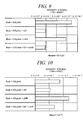
- FIG. 8 is a graph showing a measurement result of a leakage current density of a low dielectric insulating film
- FIG. 9 is a graph showing a measurement result of a moisture amount of a low dielectric insulating film
- FIG. 10 is a graph showing a measurement result of an amount of fluorine components of a low dielectric insulating film
- FIG. 11 is a cross sectional view illustrating a schematic configuration of a processing unit for performing a UV process and a silylation process
- FIG. 12 is a flowchart for describing a process sequence for forming a groove wiring having a single damascene structure
- FIGS. 13A to 13H are diagrams schematically illustrating a change in the shape of the groove wiring formed according to the process sequence of FIG. 12 ;
- FIG. 14 is a flowchart for describing a process sequence for forming a groove wiring having a dual damascene structure
- FIGS. 15A to 15I are diagrams schematically illustrating a change in the shape of the groove wiring formed according to the process sequence of FIG. 14 ;
- FIG. 16 is a flowchart for describing another process sequence for forming a groove wiring having a single damascene structure.
- FIGS. 17A to 17H are diagrams schematically illustrating a change in the shape of the groove wiring formed according to the process sequence of FIG. 16 .
- FIG. 1 is a plane view illustrating a schematic configuration of a semiconductor device manufacturing apparatus 100 in accordance with an embodiment of the present invention.
- the semiconductor device manufacturing apparatus 100 includes an etching processing unit 51 for performing a plasma etching process on a substrate (a semiconductor wafer in the present embodiment); an ashing processing unit 52 for performing an ashing process using CO 2 plasma; an UV processing unit 53 for performing an UV process; and a silylation processing unit 54 for performing a silylation process.
- These processing units 51 to 54 are installed at four sides of a hexagonal wafer transfer chamber 55 , respectively.
- load lock chambers 56 and 57 are respectively installed at two remaining sides of the wafer transfer chamber 55 .
- a wafer loading/unloading chamber 58 is provided at a load lock chambers 56 and 57 ′ side opposite to the wafer transfer chamber 55 , and three ports 59 to 61 for holding three carriers C capable of accommodating wafers W therein are provided at a wafer loading/unloading chamber 58 ′ side opposite to the load lock chambers 56 and 57 .
- the etching processing unit 51 , the ashing processing unit 52 , the UV processing unit 53 , the silylation processing unit 54 and the load lock chambers 56 and 57 are connected to the respective sides of the wafer transfer chamber 55 via gate valves G, as shown in FIG. 1 , so that they are allowed to communicate with the wafer transfer chamber 55 when the gate valves G are opened and they can be isolated from the wafer transfer chamber 55 when the gate valves G are closed.
- the gate valves G are also installed at positions where the load lock chambers 56 and 57 are connected to the wafer loading/unloading chamber 58 , so that the load lock chambers 56 and 57 are allowed to communicate with the wafer loading/unloading chamber 58 when the gate valves G are opened and they can be isolated from the wafer loading/unloading chamber 58 when the gate valves G are closed.
- a wafer transfer mechanism 62 which performs loading and unloading of a wafer W with respect to the etching processing unit 51 , the ashing processing unit 52 , the UV processing unit 53 , the silylation processing unit 54 , and the load lock chambers 56 and 57 .
- the wafer transfer mechanism 62 is positioned substantially at the center of the wafer transfer chamber 55 , and it includes a rotatable•extendible/retractable unit 63 that can make retracting, extending and rotating motions.
- the rotatable•extendible/retractable unit 63 there are provided two blades 64 a and 64 b for holding the wafer W, and the two blades 64 a and 64 b are fixed to the rotatable extendible/retractable unit 63 such that they can be oriented in an opposite direction to each other. Moreover, the interior of the wafer transfer chamber 55 is maintained at a specific vacuum level.
- a non-illustrated HEPA filter is provided in a ceiling portion of the wafer loading/unloading chamber 58 . Clean air which has passed the HEPA filter is supplied into the wafer loading/unloading chamber 58 in a down-flow state to ensure that the tasks of loading and unloading the wafer W are carried out in a clean-air atmosphere under an atmospheric pressure.
- Each of the wafer loading/unloading chamber 58 's three ports 59 , 60 and 61 for holding the carriers C is provided with a non-illustrated shutter.
- the carriers C each accommodating wafers W therein or remaining empty, are directly installed on the ports 59 , 60 and 61 , and the shutters are then opened so that the carriers C are allowed to communicate with the wafer loading/unloading chamber 58 while introduction of exterior air is prevented. Furthermore, an alignment chamber 65 is provided on a lateral side of the wafer loading/unloading chamber 58 , and alignment of the wafer W is performed therein.
- a wafer transfer mechanism 66 Disposed in the wafer loading/unloading chamber 58 is a wafer transfer mechanism 66 which performs loading and unloading of the wafer W with respect to the carriers C and the load lock chambers 56 and 57 .
- the wafer transfer mechanism 66 has a multi-joint arm structure and is capable of moving along a rail 68 in an arrangement direction of the carriers C.
- the wafer transfer mechanism 66 is configured to transfer the wafer W by holding the wafer W with a hand provided at a leading end thereof.
- the entire system including the wafer transfer mechanisms 62 and 66 is controlled by a control unit 69 .
- each of the etching processing unit 51 and the asking processing unit 52 may be implemented by, for example, a capacitively coupled plasma processing apparatus which generates plasma by applying a high frequency power between parallel plate electrodes provided in a processing chamber. Since such a plasma processing apparatus is well-known, detailed description thereof will be omitted herein.
- FIG. 2 is a longitudinal cross sectional view illustrating a schematic configuration of the UV processing unit 53 .
- the UV processing unit 53 includes a chamber 31 for accommodating the wafer W therein, and the chamber 31 is provided with an opening 32 through which the wafer W is loaded and unloaded.
- the opening 32 is connected with the wafer transfer chamber 55 via the gate valve G.
- a hot plate 33 Disposed in the chamber 31 is a hot plate 33 for mounting the wafer W and capable of heating the wafer W to a preset temperature.
- a UV lamp 34 for irradiating UV to the wafer W is installed in a ceiling portion of the chamber 31 to face the hot plate 33 .
- a gas exhaust pipe 35 for evacuating the inside of the chamber 31 and a nitrogen gas supply pipe 36 for supplying a nitrogen gas into the chamber 31 are connected to the chamber 31 to allow the UV irradiation to be carried out in the chamber 31 under a vacuum atmosphere or in a nitrogen gas atmosphere.
- FIG. 3 is a longitudinal cross sectional view illustrating a schematic configuration of the silylation processing unit 54 .
- the silylation processing unit 54 includes a chamber 41 for accommodating the wafer W therein, and the chamber 41 is provided with a non-illustrated opening through which the wafer W is loaded and unloaded. The opening for the loading and unloading of the wafer W is connected to the wafer transfer chamber 55 via the gate valve G.
- a hot plate 42 is installed in the chamber 41 , and a nitrogen gas containing a silylating agent such as TMSDMA vapor is supplied into the chamber 41 from a vicinity of the hot plate 42 .
- liquid TMSDMA is vaporized by a vaporizer 43 and is contained in the nitrogen gas in a vaporizer 43
- TMSDMA vapor a vaporized TMSDMA gas
- the introduction of the TMSDMA gas into the chamber 41 can be readily carried out by using a pressure difference between the vaporizer 43 and the chamber 41 .
- the temperature of the hot plate 42 can be controlled within a range of, e.g., about 50° C. to 200° C., and pins 44 for supporting the wafer W are provided on the surface of the hot plate 42 . Since the wafer W is not directly placed on the hot plate 42 , contamination of the rear surface of the wafer W can be prevented.
- a gas exhaust port 47 is provided at a substantially central portion of a ceiling portion of the chamber 41 to exhaust the TMSDMA-containing nitrogen gas supplied into the chamber 41 , and the gas exhaust port 47 is connected with a vacuum pump 49 via a pressure controller 48 .
- the silylation processing unit 54 includes a non-illustrated water vapor supply mechanism so that a nitrogen gas containing a certain concentration of water vapor (or only the water vapor) can be supplied into the chamber 41 .
- the silylation processing unit 54 is configured to be capable of supplying water vapor into the chamber 41 and enabling a proper absorption reaction at the damaged portion intentionally, thus facilitating a silylation reaction. Further, since the silylation reaction may be suppressed as opposed to the original intention if the absorption reaction progresses excessively, the supply of the water vapor needs to be controlled so as not to cause such suppression of the reaction.
- FIG. 4 is a flowchart illustrating a process sequence of the semiconductor device manufacturing method in accordance with the embodiment of the present invention
- FIGS. 5A to 5E are enlarged diagrams illustrating cross sectional views of a wafer processed in respective steps of FIG. 4 .
- a wafer W is provided with a low dielectric insulating film (Low-k film) 71 formed on a base layer 70 made of silicon or the like by coating, CVD, or the like.
- a photoresist film 72 is formed on the low dielectric insulating film 71 , and the photoresist film 72 serves as a mask having a preset pattern formed by an exposure and development process or the like.
- the wafer W in this state is loaded into the semiconductor device manufacturing apparatus 100 .
- the wafer W is first loaded into the etching processing unit 52 by the wafer transfer mechanism 62 in the wafer transfer chamber 55 and is etched therein by, e.g., CF 4 plasma or the like (step 1 of FIG. 4 ).
- CF 4 plasma or the like
- a hole (or groove) 73 which reaches the base layer is formed in the low dielectric insulating film 71 by using the photoresist film 72 as a mask, as depicted in FIG. 5B .
- a reference numeral 71 a in FIG. 5B indicates a damaged portion of the low dielectric insulating film 71 which is caused by the plasma etching.
- the wafer W is transferred from the etching processing unit 51 into the ashing processing unit 52 by the wafer transfer mechanism 62 in the wafer transfer chamber 55 .
- an ashing process by, e.g., CO 2 plasma is conducted (step 2 of FIG. 4 ).
- the photoresist mask 72 used as the mask in the etching process is removed, as illustrated in FIG. 5C .
- a damage different from that caused in the etching process is inflicted on the damaged portion 71 a again.
- the wafer W is transferred from the ashing processing unit 52 into the UV processing unit 53 by the wafer transfer mechanism 62 in the wafer transfer chamber 55 .
- a UV process for irradiating UV to the wafer W (low dielectric insulating film 71 ) is performed, as shown in FIG. 5D (step 3 of FIG. 4 ).
- the UV process by the UV processing unit 53 is carried out by irradiating UV to the entire surface of the wafer W while heating the wafer W to, e.g., about 300° C. This UV process may be performed in a vacuum atmosphere or in a nitrogen gas atmosphere.
- the wafer W is transferred from the UV processing unit 53 into the silylation processing unit 54 by the wafer transfer mechanism 62 in the wafer transfer chamber 55 .
- a silylation process is performed in the silylation processing unit 54 (step 4 of FIG. 4 ).
- the silylation process by the silylation processing unit 54 is carried out by exposing the wafer W to the silylating agent such as the TMSDMA vapor or the like, as illustrated in FIG. 5E .
- Processing conditions for the silylation process may be selected depending on the kind of the silylating agent.
- the temperature of the vaporizer 43 may be appropriately set to range from a room temperature to about 50° C.; the flow rates of the silylating agent and the N 2 gas (purge gas) may be appropriately set to be in the range of about 0.1 to 1.0 g/min and in the range of about 1 to 10 L/min, respectively; a processing pressure may be appropriately set to range from about 666 to 95976 Pa (5 to 720 Torr); and the temperature of the hot plate 42 may be appropriately set to range from a room temperature to about 200° C.
- the wafer W is transferred into the load lock chamber 56 or 57 by the wafer transfer mechanism 62 in the wafer transfer chamber 55 and then is unloaded from the load lock chamber 56 or 57 into a normal pressure atmosphere.
- the sidewall of the hole (or groove) 73 formed in the low dielectric insulating film 71 is damaged by the etching process using the CF 4 plasma or the like and the asking process using the CO 2 plasma or the like.
- the damaged portion may react with moisture, whereby a methyl group would decrease and a hydroxyl group would increase in the vicinity of the sidewall of the hole (or groove) 73 , resulting in an increase of dielectric constant.
- damaged portion 71 a is schematically illustrated in FIGS. 5B and 5C , a boundary between the damaged portion 71 a and an undamaged portion is not actually as clear as shown in FIGS. 5B and 5C .
- the UV process by the UV processing unit 53 and the silylation process by the silylation processing unit 54 are performed to recover the damage of the low dielectric insulating film 71 .
- the damage of the low dielectric insulating film 71 it is possible to form a wiring having highly advantageous electrical characteristics, thus enabling an improvement of reliability of a semiconductor device.
- the above-stated respective processes are performed by a single apparatus, i.e., by the semiconductor device manufacturing apparatus 100 including the etching processing unit 51 , the asking processing unit 52 and the UV processing unit 53 and the silylation processing unit 54 integrated as one body, it may be also possible to perform the respective processes by individual apparatuses. For example, it may be possible to perform the etching process and the ashing process by a single apparatus and to perform the UV process and the silylation process by a UV process apparatus and a silylation process apparatus.
- FIG. 6 is a graph showing an analysis result of a wafer on which an etching process of a low dielectric insulating film, an ashing process by CO 2 plasma, an UV process and a silylation process were performed in accordance with the above-described embodiment; and a wafer on which a conventional method of performing only an etching process of a low dielectric insulating film, an ashing process by CO 2 plasma and a silylation process was carried out without performing a UV process.
- the analysis was performed by using a fourier transform infrared spectrometer. As depicted in FIG.
- FIG. 7 shows, in sequence from the top, measurement results of dielectric constants (k values) of low dielectric insulating films in respective cases of performing only an etching process and an ashing process; only a UV process after the etching and the ashing processes; only a silylation process (LKR) after the etching and the ashing processes; and both the UV process and the silylation process (LKR) after the etching and the ashing processes.
- the dielectric constant of the low dielectric insulating film was about 2.4 before the etching process and the ashing process, and a porous MSQ (Methyl Silses Quioxane) was used as the low dielectric insulating film.
- the dielectric constant of the low dielectric insulating film cannot be reduced when only the silylation process (LKR) is performed after the etching process and the ashing process, the dielectric constant of the low dielectric insulating film can be decreased by performing the UV process. Furthermore, in the example shown in FIG. 7 (the second one from the top), the dielectric constant of the low dielectric insulating film is reduced by performing only the UV process without performing the silylation process.
- LLR silylation process
- the UV process is basically not a reaction for allowing a film to have a hydrophobic property, so that the insulating film's portion whose dielectric constant is reduced by the UV process may be dissolved in a hydrofluoric acid based solution or the like which may be used in a post process.
- the hydrophobic property of the film surface desirably needs to be as high as possible, and it is therefore desirable to perform the silylation process (LKR) as well as the UV process.
- FIG. 8 shows, in sequence from the top, measurement results of leakage current densities in respective cases of performing only the etching process and the ashing process; only the UV process after the etching and the ashing processes; only the silylation process (LKR) after the etching and the ashing processes; and both the UV process and the silylation process (LKR) after the etching and the ashing processes.
- the left side of FIG. 8 indicates a case of applying an electric field of about 1 MV/cm and the right side thereof indicates a case of applying an electric field of about 2 MV/cm.
- the measurements of the leakage current densities and the above-stated dielectric constants were carried out by performing the above-described respective processes on the low dielectric insulating film formed on the entire surface of the wafer; forming an electrode made of a aluminum film on the surface thereof by using a sputtering method; and then applying a voltage between the front surface and the rear surface of the wafer. Further, a porous MSQ (Methyl Silses Quioxane) was used as the low dielectric insulating film.
- MSQ Metal Silses Quioxane
- FIG. 9 shows, in sequence from the top, measurement results of moisture amounts in low dielectric insulating films in respective cases of performing only the etching process and the ashing process; only the UV process after the etching and the ashing processes; only the silylation process (LKR) after the etching and the ashing processes; and both the UV process and the silylation process (LKR) after the etching and the ashing processes.
- the moisture amount is slightly reduced when only the silylation process (LKR) is performed after the etching process and the ashing process, the moisture amount can be reduced to about 1 ⁇ 3 by performing the UV process.
- LLR silylation process
- moisture increases the mobility of electric charges, it causes an increase of a leakage current between wirings. If a film absorbs moisture, it implies that the film has a structure readily allowing a movement of electric charges. Further, since water itself has a high dielectric constant, it may cause an increase of the dielectric constant of the low dielectric insulating film. In addition, since the moisture serves as a factor that oxidizes a metal wiring such as Cu, it may leads to an increase of wiring resistance, resulting in an increase of power consumption. In consideration of the above-mentioned reasons, it is desirable to reduce the moisture amount in the low dielectric insulating film.
- FIG. 10 shows, in sequence from the top, measurement results of the amount of fluorine components of low dielectric insulating films in respective cases of performing only the etching process and the ashing process; only the UV process after the etching and the ashing processes; only the silylation process (LKR) after the etching and the ashing processes; and both the UV process and the silylation process (LKR) after the etching and the ashing processes.
- the fluorine components are not reduced when only the silylation process (LKR) is performed after the etching process and the ashing process, the fluorine components can be reduced to about 2 ⁇ 3 by performing the UV process.
- LLR silylation process
- fluorine Since fluorine has high electronegativity, it is highly likely that the polarity of the film structure of the low dielectric insulating film may be increased if the fluorine remains in the low dielectric insulating film. Thus, by attracting moisture, the dielectric constant may increase, whereby the dielectric constant of the insulating film itself is highly likely to increase. Further, in case that the fluorine remains in the low dielectric insulating film, there is a likelihood that the fluorine may be ionized by a slight amount of water in the atmospheric atmosphere or the insulating film with the lapse of time, resultantly dissolving the low dielectric insulating film. In view of the forgoing reasons, it is desirable to reduce the fluorine components in the low dielectric insulating film.
- FIG. 11 illustrates a configuration of a UV processing unit 53 a configured to perform a UV process and a silylation process (LKR) in a single chamber.
- the UV processing unit 53 a includes a chamber 31 for accommodating a wafer W therein, and the chamber 31 is provided with an opening 32 through which the wafer W is loaded and unloaded.
- the opening 32 is connected with the wafer transfer chamber 55 via the above-described gate valve G.
- a hot plate 33 for holding the wafer W and heating the wafer to a preset temperature.
- a UV lamp 34 for irradiating UV to the wafer W is installed in a ceiling portion of the chamber 31 to face the hot plate 33 .
- a nitrogen gas supply pipe 36 for supplying a nitrogen gas into the chamber 31 is connected to the ceiling portion inside the chamber 31
- a TMSDMA vapor supply pipe 136 for supplying vapor of a silylating agent (TMSDMA in the present embodiment) into the chamber 31 is also connected to the ceiling portion inside the chamber independently of the nitrogen gas supply pipe 36 .
- a gas exhaust pipe 35 for evacuating the inside of the chamber 31 is also connected to the chamber 31 .
- a UV process can be performed in the chamber 31 under a vacuum atmosphere or a nitrogen gas atmosphere. Further, a silylation process can be consecutively performed in the same chamber 31 under a mixed atmosphere of a nitrogen gas and TMSDMA vapor by introducing the TMSDMA vapor from the TMSDMA vapor supply pipe 136 while concurrently introducing the nitrogen gas from the nitrogen gas supply pipe 36 .
- FIG. 12 is a flowchart for illustrating a process sequence for forming a groove wiring having a single damascene structure
- FIGS. 13A to 13H are diagrams schematically showing a change of the shape of the groove wiring formed in each process of FIG. 12 .
- a wafer W (wafer W itself is not illustrated) including an insulating film 170 in which a lower wiring (Cu wiring) 172 is formed with a barrier metal layer 171 therebetween and a stopper film 173 made of, e.g., a SiN film or a SiC film formed on the surface of the insulating film 170 .
- an antireflection film 175 a and a resist film 175 b are sequentially formed on the interlayer insulating film 174 , and by performing an exposure and development process, the resist film 175 b becomes a resist mask with a preset pattern (step 102 , FIG. 13B ).
- an etching process for etching the interlayer insulating film 174 is performed by using the resist mask, whereby a via 178 a that reaches the stopper film 173 is formed in the interlayer insulating film 174 (step 103 , FIG. 13C ).
- an asking process for removing the antireflection film 175 a and the resist film 175 b is performed by CO 2 plasma (step 104 , FIG. 13D ).
- a reference numeral 179 a indicates a damaged portion.
- step 105 there is performed a modification process for modifying polymer residues or the like remaining on the wafer W after the etching or the ashing process, thus rendering them water soluble. Thereafter, a cleaning process for removing the modified polymer residues or the like is conducted (step 106 ).
- the sidewall of the via 178 a formed in the interlayer insulating film 174 is damaged by the etching process, the ashing process, or the subsequent washing process.
- the damaged portion reacts with moisture, whereby a methyl group decreases and a hydroxyl group increases in the vicinity of the sidewall of the via 178 a , resulting in an increase of dielectric constant.
- the via 178 a is later filled with a metal material to form a groove wiring in the state that such a damaged portion exists on the sidewall of the via 178 a , a parasitic capacitance between wirings would be increased, resulting in problems such as a signal delay, a deterioration of insulation between the groove wirings, and so forth.
- the damaged portion 179 a is schematically illustrated in FIGS. 13C and 13D , a boundary between the damaged portion 179 a and an undamaged portion is not actually as clear as shown in FIGS. 13C and 13D .
- a UV process for irradiating UV to the wafer W is performed (step 107 ), and a silylation process is then carried out (step 108 ), whereby the damaged portion 179 a of the interlayer insulating film 174 is recovered ( FIG. 13E ).
- an etching process for removing the stopper film 173 is performed (step 109 ), and a cleaning process for removing etched residues is then conducted (step 110 , FIG. 13F ).
- the sidewall of the via 178 a formed in the interlayer insulating film 174 may be damaged by this etching process or the cleaning process again, so that a damaged portion 179 b is formed.
- a UV process for irradiating UV to the wafer W is subsequently conducted (step 111 ), and a silylation process is then carried out (step 112 ), whereby the damaged portion 179 b of the interlayer insulating film 174 is recovered ( FIG. 13G ).
- a barrier metal film and a Cu seed layer are formed on the inner wall of the via 178 a (step 113 ).
- the via 178 a is filled with a metal 176 such as copper by electroplating (step 114 ).
- an annealing process of the metal 176 buried in the via 178 a is performed by heating the wafer W, and a planarization process is performed by a CMP method (step 115 , FIG. 13H ).
- the damaged portion can be recovered by the UV process and the silylation process.
- a groove wiring having advantageous electrical characteristics can be formed, so that the reliability of the semiconductor device can be improved.
- FIG. 14 is a flowchart for illustrating a process sequence for forming a groove wiring having a dual damascene structure
- FIGS. 15A to 15I are diagrams schematically showing a change of the shape of the groove wiring formed in each process of FIG. 14 .
- a wafer W (wafer W itself is not illustrated) including an insulating film 170 in which a lower wiring (Cu wiring) 172 is formed with a barrier metal layer 171 therebetween and a stopper film 173 made of, e.g., a SiN film or a SiC film formed on the surface of the insulating film 170 .
- an antireflection film 175 a and a resist film 175 b are sequentially formed on the interlayer insulating film 174 . Thereafter, a resist mask having a preset pattern is obtained by exposing and developing the resist film 175 b (step 202 , FIG. 15B ).
- a reference numeral 179 a indicates a damaged portion generated by the etching process.
- an ashing process is performed by CO 2 plasma, whereby the antireflection film 175 a and the resist film 175 b are removed (step 204 ), and a cleaning process for removing polymer residues or the like generated by the previous etching process or ashing process is carried out (step 205 ).
- a UV process for irradiating UV to the wafer W is performed (step 206 ), and a silylation process is subsequently carried out (step 207 ), whereby the damaged portion 179 a of the interlayer insulating film 174 is recovered ( FIG. 15D ).
- a protective film 181 is formed on the surface of the interlayer insulating film 174 (step 208 ). Then, an antireflection film 182 a and a resist film 182 b are sequentially formed on the protective film 181 , and the resist film 182 b is subjected to an exposure and development process using a preset pattern, so that the resist film 182 b becomes a resist mask having the preset pattern (step 209 , FIG. 15E ).
- the protective film 181 can be formed by spin-coating a preset liquid chemical.
- the protective film 181 is optional, and thus it may be possible to form the antireflection film 182 a and the resist film 182 b directly on the interlayer insulating film 174 .
- an etching process is performed by using the resist mask made of the resist film 182 b , whereby a trench 178 b is formed in the interlayer insulating film 174 (step 210 , FIG. 15F ). Then, the resist film 182 b and the antireflection film 182 a are removed by an ashing process using CO 2 plasma (step 211 ).
- a reference numeral 179 b shown in FIG. 15F is a damaged portion caused by the etching process in step 210 .
- a cleaning process for removing polymer residues generated by the previous etching or ashing process, the protective film 181 , and the like are carried out (step 212 ).
- a UV process for irradiating UV to the wafer W is conducted (step 213 ), and a silylation process is subsequently performed (Step 214 ), whereby the damaged portion 179 b of the interlayer insulating film 174 is recovered ( FIG. 15G ).
- FIG. 15H illustrates a state after the completion of the silylation process.
- a barrier metal film and a Cu seed layer are formed on the inner walls of the via 178 a and the trench 178 b ; a plug is formed by filling the via 178 a and the trench 178 b with a metal 176 such as copper by electroplating; an annealing process of the metal 176 buried in the via 178 a and the trench 178 b is performed by heating the wafer W; and a planarization process is performed by a CMP method (step 218 , FIG. 15I ).
- FIG. 16 is a flowchart for illustrating another process sequence for forming a groove wiring having a dual damascene structure
- FIGS. 17A to 17H are diagrams schematically showing a change of the shape of the groove wiring formed in each process of FIG. 16 .
- a wafer W (wafer W itself is not illustrated) including an insulating film 170 in which a lower wiring (Cu wiring) 172 is formed with a barrier metal layer 171 therebetween and a stopper film 173 made of, e.g., a SiN film or a SiC film formed on the surface of the insulating film 170 .
- An interlayer insulating film 174 made of a low dielectric insulating film (for example, porous MSQ or the like), a hard mask layer 186 , an antireflection film 187 a and a resist film 187 b are sequentially formed on the stopper film 173 of the wafer W, and a resist mask is obtained by exposing and developing the resist film 187 b by using a preset pattern (step 301 , FIG. 17A ).
- an etching process is performed by using the resist film 187 b as an etching mask (step 302 ) to thereby pattern the hard mask layer 186 , and the antireflection film 187 a and the resist film 187 b are then removed (step 303 , FIG. 17B ).
- an antireflection film 188 a and a resist film 188 b are sequentially formed on the hard mask layer 186 , and a resist mask is obtained by exposing and developing the resist film 188 b by using a preset pattern (step 304 , FIG. 17C ).
- a via 178 a that reaches the stopper film 173 is formed by using the resist mask made of the resist film 188 b (step 305 , FIG. 17D ). Then, the resist film 188 b and the antireflection film 188 a are removed by an ashing process using CO 2 plasma or the like and a polymer residue removing•cleaning process is conducted (step 306 , FIG. 17E ).
- a UV process and a silylation process may be conducted subsequently.
- a trench 178 b is formed by performing an etching process while using the hard mask layer 186 as an etching mask (step 307 ). At this time, if a damaged portion is generated at the interlayer insulating film 174 , a UV process and a silylation process can be immediately performed.
- the hard mask layer 186 is removed by an asking process using CO 2 plasma or a liquid chemical process (step 308 , FIG. 17F ).
- a UV process and a silylation process are conducted after the removal of the hard mask layer 186 (step 309 ), whereby a damaged portion generated at the interlayer insulating film 174 in or before step 308 can be recovered.
- FIG. 17F shows a state after the damage is recovered.
- an etching process for removing the stopper film 173 and a residue removing•cleaning process are conducted (step 310 , FIG. 17G ), and a UV process and a silylation process are carried out again to recover a damaged portion generated at the via 178 a and the trench 178 b because of the etching process or the like (step 311 ).
- a barrier metal film and a Cu seed layer are formed on the inner walls of the via 178 a and the trench 178 b , and a plug is formed by filling the via 178 a and the trench 178 b with a metal 176 such as copper by electroplating, and an annealing process of the metal 176 buried in the via 178 a and the trench 178 b is performed by heating the wafer W, and a planarization process is performed by a CMP method (step 312 , FIG. 17H ).
Landscapes
- Engineering & Computer Science (AREA)
- Physics & Mathematics (AREA)
- Condensed Matter Physics & Semiconductors (AREA)
- General Physics & Mathematics (AREA)
- Manufacturing & Machinery (AREA)
- Computer Hardware Design (AREA)
- Microelectronics & Electronic Packaging (AREA)
- Power Engineering (AREA)
- Plasma & Fusion (AREA)
- Internal Circuitry In Semiconductor Integrated Circuit Devices (AREA)
- Drying Of Semiconductors (AREA)
Priority Applications (1)
| Application Number | Priority Date | Filing Date | Title |
|---|---|---|---|
| US13/329,677 US8614140B2 (en) | 2008-10-21 | 2011-12-19 | Semiconductor device manufacturing apparatus |
Applications Claiming Priority (2)
| Application Number | Priority Date | Filing Date | Title |
|---|---|---|---|
| JP2008270831A JP4708465B2 (ja) | 2008-10-21 | 2008-10-21 | 半導体装置の製造方法及び半導体装置の製造装置 |
| JP2008-270831 | 2008-10-21 |
Related Child Applications (1)
| Application Number | Title | Priority Date | Filing Date |
|---|---|---|---|
| US13/329,677 Division US8614140B2 (en) | 2008-10-21 | 2011-12-19 | Semiconductor device manufacturing apparatus |
Publications (2)
| Publication Number | Publication Date |
|---|---|
| US20100099256A1 US20100099256A1 (en) | 2010-04-22 |
| US8101507B2 true US8101507B2 (en) | 2012-01-24 |
Family
ID=42109018
Family Applications (2)
| Application Number | Title | Priority Date | Filing Date |
|---|---|---|---|
| US12/580,495 Expired - Fee Related US8101507B2 (en) | 2008-10-21 | 2009-10-16 | Semiconductor device manufacturing method and semiconductor device manufacturing apparatus |
| US13/329,677 Active 2029-12-24 US8614140B2 (en) | 2008-10-21 | 2011-12-19 | Semiconductor device manufacturing apparatus |
Family Applications After (1)
| Application Number | Title | Priority Date | Filing Date |
|---|---|---|---|
| US13/329,677 Active 2029-12-24 US8614140B2 (en) | 2008-10-21 | 2011-12-19 | Semiconductor device manufacturing apparatus |
Country Status (5)
| Country | Link |
|---|---|
| US (2) | US8101507B2 (zh) |
| JP (1) | JP4708465B2 (zh) |
| KR (1) | KR101046256B1 (zh) |
| CN (1) | CN101728320B (zh) |
| TW (1) | TWI383451B (zh) |
Cited By (2)
| Publication number | Priority date | Publication date | Assignee | Title |
|---|---|---|---|---|
| US20120264308A1 (en) * | 2011-04-14 | 2012-10-18 | Tokyo Electron Limited | Etching method, etching apparatus and storage medium |
| US9929098B2 (en) | 2015-03-30 | 2018-03-27 | Samsung Electronics Co., Ltd. | Copper via with barrier layer and cap layer |
Families Citing this family (21)
| Publication number | Priority date | Publication date | Assignee | Title |
|---|---|---|---|---|
| US9659769B1 (en) | 2004-10-22 | 2017-05-23 | Novellus Systems, Inc. | Tensile dielectric films using UV curing |
| US8889233B1 (en) | 2005-04-26 | 2014-11-18 | Novellus Systems, Inc. | Method for reducing stress in porous dielectric films |
| US8980769B1 (en) | 2005-04-26 | 2015-03-17 | Novellus Systems, Inc. | Multi-station sequential curing of dielectric films |
| US10037905B2 (en) | 2009-11-12 | 2018-07-31 | Novellus Systems, Inc. | UV and reducing treatment for K recovery and surface clean in semiconductor processing |
| US8465991B2 (en) | 2006-10-30 | 2013-06-18 | Novellus Systems, Inc. | Carbon containing low-k dielectric constant recovery using UV treatment |
| US9050623B1 (en) | 2008-09-12 | 2015-06-09 | Novellus Systems, Inc. | Progressive UV cure |
| JP4927158B2 (ja) * | 2009-12-25 | 2012-05-09 | 東京エレクトロン株式会社 | 基板処理方法、その基板処理方法を実行させるためのプログラムを記録した記録媒体及び基板処理装置 |
| JP2012015197A (ja) * | 2010-06-29 | 2012-01-19 | Tokyo Electron Ltd | 半導体装置の配線形成方法、半導体装置の製造方法および半導体装置の配線形成システム |
| JP5782279B2 (ja) * | 2011-01-20 | 2015-09-24 | 株式会社Screenホールディングス | 基板処理方法および基板処理装置 |
| JP5941623B2 (ja) * | 2011-03-25 | 2016-06-29 | 東京エレクトロン株式会社 | 処理方法および記憶媒体 |
| JP5976776B2 (ja) * | 2011-04-08 | 2016-08-24 | アプライド マテリアルズ インコーポレイテッドApplied Materials,Incorporated | Uv処理、化学処理、および堆積のための装置および方法 |
| CN102364669A (zh) * | 2011-09-15 | 2012-02-29 | 上海华力微电子有限公司 | 超低介电常数薄膜铜互连的制作方法 |
| CN102683268A (zh) * | 2012-02-28 | 2012-09-19 | 上海华力微电子有限公司 | 具超低介电常数层间介电质的双大马士革结构的形成方法 |
| JP5898549B2 (ja) * | 2012-03-29 | 2016-04-06 | 株式会社Screenホールディングス | 基板処理方法および基板処理装置 |
| TW201403711A (zh) * | 2012-07-02 | 2014-01-16 | Applied Materials Inc | 利用氣相化學暴露之低k介電質損傷修復 |
| JP6054279B2 (ja) * | 2013-10-17 | 2016-12-27 | 東京エレクトロン株式会社 | 金属配線層形成方法、金属配線層形成装置および記憶媒体 |
| US9887160B2 (en) * | 2015-09-24 | 2018-02-06 | International Business Machines Corporation | Multiple pre-clean processes for interconnect fabrication |
| KR20180030280A (ko) | 2016-09-12 | 2018-03-22 | 삼성전자주식회사 | 배선 구조체를 갖는 반도체 소자 |
| US9847221B1 (en) | 2016-09-29 | 2017-12-19 | Lam Research Corporation | Low temperature formation of high quality silicon oxide films in semiconductor device manufacturing |
| US10847413B2 (en) * | 2017-11-30 | 2020-11-24 | Taiwan Semiconductor Manufacturing Company, Ltd. | Method of forming contact plugs for semiconductor device |
| TWI820189B (zh) * | 2018-08-30 | 2023-11-01 | 日商東京威力科創股份有限公司 | 基板處理方法及基板處理裝置 |
Citations (5)
| Publication number | Priority date | Publication date | Assignee | Title |
|---|---|---|---|---|
| JP2006049798A (ja) | 2004-07-02 | 2006-02-16 | Tokyo Electron Ltd | 溝配線または接続孔を有する半導体装置の製造方法 |
| KR20070019774A (ko) | 2004-07-02 | 2007-02-15 | 동경 엘렉트론 주식회사 | 반도체 디바이스의 제조 방법 |
| US20070134435A1 (en) | 2005-12-13 | 2007-06-14 | Ahn Sang H | Method to improve the ashing/wet etch damage resistance and integration stability of low dielectric constant films |
| US20080057717A1 (en) * | 2006-08-24 | 2008-03-06 | Fujitsu Limited | Semiconductor device manufacturing method |
| KR20080076847A (ko) | 2007-02-15 | 2008-08-20 | 에어 프로덕츠 앤드 케미칼스, 인코오포레이티드 | 유전체 필름의 물성을 강화하기 위한 활성 화학 공정 |
Family Cites Families (2)
| Publication number | Priority date | Publication date | Assignee | Title |
|---|---|---|---|---|
| US6331227B1 (en) * | 1999-12-14 | 2001-12-18 | Epion Corporation | Enhanced etching/smoothing of dielectric surfaces |
| US7482265B2 (en) * | 2006-01-10 | 2009-01-27 | Taiwan Semiconductor Manufacturing Company, Ltd. | UV curing of low-k porous dielectrics |
-
2008
- 2008-10-21 JP JP2008270831A patent/JP4708465B2/ja active Active
-
2009
- 2009-10-15 KR KR1020090098166A patent/KR101046256B1/ko active IP Right Grant
- 2009-10-16 US US12/580,495 patent/US8101507B2/en not_active Expired - Fee Related
- 2009-10-20 TW TW098135381A patent/TWI383451B/zh not_active IP Right Cessation
- 2009-10-20 CN CN2009102060788A patent/CN101728320B/zh not_active Expired - Fee Related
-
2011
- 2011-12-19 US US13/329,677 patent/US8614140B2/en active Active
Patent Citations (5)
| Publication number | Priority date | Publication date | Assignee | Title |
|---|---|---|---|---|
| JP2006049798A (ja) | 2004-07-02 | 2006-02-16 | Tokyo Electron Ltd | 溝配線または接続孔を有する半導体装置の製造方法 |
| KR20070019774A (ko) | 2004-07-02 | 2007-02-15 | 동경 엘렉트론 주식회사 | 반도체 디바이스의 제조 방법 |
| US20070134435A1 (en) | 2005-12-13 | 2007-06-14 | Ahn Sang H | Method to improve the ashing/wet etch damage resistance and integration stability of low dielectric constant films |
| US20080057717A1 (en) * | 2006-08-24 | 2008-03-06 | Fujitsu Limited | Semiconductor device manufacturing method |
| KR20080076847A (ko) | 2007-02-15 | 2008-08-20 | 에어 프로덕츠 앤드 케미칼스, 인코오포레이티드 | 유전체 필름의 물성을 강화하기 위한 활성 화학 공정 |
Non-Patent Citations (2)
| Title |
|---|
| Japanese Office action for 2008-270831 dated Nov. 9, 2010. |
| Korean Office action for 10-2009-0098166 dated Mar. 28, 2011. |
Cited By (3)
| Publication number | Priority date | Publication date | Assignee | Title |
|---|---|---|---|---|
| US20120264308A1 (en) * | 2011-04-14 | 2012-10-18 | Tokyo Electron Limited | Etching method, etching apparatus and storage medium |
| US8969218B2 (en) * | 2011-04-14 | 2015-03-03 | Tokyo Electron Limited | Etching method, etching apparatus and storage medium |
| US9929098B2 (en) | 2015-03-30 | 2018-03-27 | Samsung Electronics Co., Ltd. | Copper via with barrier layer and cap layer |
Also Published As
| Publication number | Publication date |
|---|---|
| US8614140B2 (en) | 2013-12-24 |
| CN101728320A (zh) | 2010-06-09 |
| JP2010103151A (ja) | 2010-05-06 |
| JP4708465B2 (ja) | 2011-06-22 |
| TW201030842A (en) | 2010-08-16 |
| TWI383451B (zh) | 2013-01-21 |
| KR20100044097A (ko) | 2010-04-29 |
| KR101046256B1 (ko) | 2011-07-05 |
| US20100099256A1 (en) | 2010-04-22 |
| CN101728320B (zh) | 2011-11-02 |
| US20120132365A1 (en) | 2012-05-31 |
Similar Documents
| Publication | Publication Date | Title |
|---|---|---|
| US8614140B2 (en) | Semiconductor device manufacturing apparatus | |
| US8075730B2 (en) | Apparatus for manufacturing a semiconductor device | |
| KR100810163B1 (ko) | 반도체 장치의 제조 방법, 기판 처리 시스템 및 기록 매체 | |
| KR100904105B1 (ko) | 반도체 장치의 제조 방법 | |
| US8187981B2 (en) | Substrate processing method, substrate processing system, and computer-readable storage medium | |
| KR101143727B1 (ko) | 반도체 장치의 제조 방법 및 기억 매체 | |
| JP2009010043A (ja) | 基板処理方法,基板処理装置,記録媒体 | |
| JP2002353308A (ja) | 半導体装置及びその製造方法 | |
| US8288252B2 (en) | Method for recovering damaged components in lower region of low dielectric insulating film | |
| US7799703B2 (en) | Processing method and storage medium | |
| JPWO2020016915A1 (ja) | 半導体装置の製造方法、基板処理装置およびプログラム | |
| US8870164B2 (en) | Substrate processing method and storage medium | |
| KR100870806B1 (ko) | 반도체 디바이스의 제조 방법 | |
| JP2007123412A (ja) | 半導体装置の製造方法 | |
| TW201308426A (zh) | 處理方法及記憶媒體 |
Legal Events
| Date | Code | Title | Description |
|---|---|---|---|
| AS | Assignment |
Owner name: TOKYO ELECTRON LIMITED,JAPAN Free format text: ASSIGNMENT OF ASSIGNORS INTEREST;ASSIGNORS:ASAKO, RYUICHI;SHIRAISHI, GOUSUKE;TAHARA, SHIGERU;SIGNING DATES FROM 20090821 TO 20090831;REEL/FRAME:023383/0878 Owner name: TOKYO ELECTRON LIMITED, JAPAN Free format text: ASSIGNMENT OF ASSIGNORS INTEREST;ASSIGNORS:ASAKO, RYUICHI;SHIRAISHI, GOUSUKE;TAHARA, SHIGERU;SIGNING DATES FROM 20090821 TO 20090831;REEL/FRAME:023383/0878 |
|
| ZAAA | Notice of allowance and fees due |
Free format text: ORIGINAL CODE: NOA |
|
| ZAAB | Notice of allowance mailed |
Free format text: ORIGINAL CODE: MN/=. |
|
| STCF | Information on status: patent grant |
Free format text: PATENTED CASE |
|
| CC | Certificate of correction | ||
| FEPP | Fee payment procedure |
Free format text: PAYOR NUMBER ASSIGNED (ORIGINAL EVENT CODE: ASPN); ENTITY STATUS OF PATENT OWNER: LARGE ENTITY Free format text: PAYER NUMBER DE-ASSIGNED (ORIGINAL EVENT CODE: RMPN); ENTITY STATUS OF PATENT OWNER: LARGE ENTITY |
|
| FPAY | Fee payment |
Year of fee payment: 4 |
|
| MAFP | Maintenance fee payment |
Free format text: PAYMENT OF MAINTENANCE FEE, 8TH YEAR, LARGE ENTITY (ORIGINAL EVENT CODE: M1552); ENTITY STATUS OF PATENT OWNER: LARGE ENTITY Year of fee payment: 8 |
|
| FEPP | Fee payment procedure |
Free format text: MAINTENANCE FEE REMINDER MAILED (ORIGINAL EVENT CODE: REM.); ENTITY STATUS OF PATENT OWNER: LARGE ENTITY |
|
| LAPS | Lapse for failure to pay maintenance fees |
Free format text: PATENT EXPIRED FOR FAILURE TO PAY MAINTENANCE FEES (ORIGINAL EVENT CODE: EXP.); ENTITY STATUS OF PATENT OWNER: LARGE ENTITY |
|
| STCH | Information on status: patent discontinuation |
Free format text: PATENT EXPIRED DUE TO NONPAYMENT OF MAINTENANCE FEES UNDER 37 CFR 1.362 |
|
| FP | Lapsed due to failure to pay maintenance fee |
Effective date: 20240124 |