US8093981B2 - Laminated inductor with enhanced current endurance - Google Patents
Laminated inductor with enhanced current endurance Download PDFInfo
- Publication number
- US8093981B2 US8093981B2 US12/712,129 US71212910A US8093981B2 US 8093981 B2 US8093981 B2 US 8093981B2 US 71212910 A US71212910 A US 71212910A US 8093981 B2 US8093981 B2 US 8093981B2
- Authority
- US
- United States
- Prior art keywords
- magnetic
- permeability
- laminated inductor
- plates
- inductor according
- Prior art date
- Legal status (The legal status is an assumption and is not a legal conclusion. Google has not performed a legal analysis and makes no representation as to the accuracy of the status listed.)
- Expired - Fee Related, expires
Links
- 230000035699 permeability Effects 0.000 claims abstract description 32
- 125000006850 spacer group Chemical group 0.000 claims abstract description 22
- 239000004020 conductor Substances 0.000 claims description 11
- 230000002708 enhancing effect Effects 0.000 abstract 1
- 239000000470 constituent Substances 0.000 description 1
- 230000004048 modification Effects 0.000 description 1
- 238000012986 modification Methods 0.000 description 1
- 238000006467 substitution reaction Methods 0.000 description 1
Images




Classifications
-
- H—ELECTRICITY
- H01—ELECTRIC ELEMENTS
- H01F—MAGNETS; INDUCTANCES; TRANSFORMERS; SELECTION OF MATERIALS FOR THEIR MAGNETIC PROPERTIES
- H01F17/00—Fixed inductances of the signal type
- H01F17/0006—Printed inductances
- H01F17/0013—Printed inductances with stacked layers
-
- H—ELECTRICITY
- H01—ELECTRIC ELEMENTS
- H01F—MAGNETS; INDUCTANCES; TRANSFORMERS; SELECTION OF MATERIALS FOR THEIR MAGNETIC PROPERTIES
- H01F17/00—Fixed inductances of the signal type
- H01F17/0006—Printed inductances
- H01F17/0033—Printed inductances with the coil helically wound around a magnetic core
-
- H—ELECTRICITY
- H01—ELECTRIC ELEMENTS
- H01F—MAGNETS; INDUCTANCES; TRANSFORMERS; SELECTION OF MATERIALS FOR THEIR MAGNETIC PROPERTIES
- H01F3/00—Cores, Yokes, or armatures
- H01F3/10—Composite arrangements of magnetic circuits
- H01F2003/106—Magnetic circuits using combinations of different magnetic materials
Definitions
- the present invention generally relates to a laminated inductor with enhanced current endurance, and more particularly to a laminated inductor that improves the characteristics of DC (direct current) superimposition and expands the applications of the laminated inductor.
- Taiwan Utility Model No. M331734 discloses a laminated inductor that enhances current endurance.
- the conventional laminated inductor is composed of a plurality of magnetic plates 71 sequentially stacked on each other. At least one spacer layer 73 is interposed between the magnetic plates 71 .
- the spacer layer 73 is formed of two magnetic plates 731 having high magnetic permeability and another magnetic plate 732 having low magnetic permeability interposed between the magnetic plates 731 .
- the topmost magnetic plate 71 is covered by a magnetic lid 74 to thereby improve the characteristics of DC superimposition of the known laminated inductor.
- the known laminated inductor is effective in improving the DC superimposition characteristics of laminated inductor.
- each of the magnetic plates 71 is only provided with a conductor pattern 73 printed thereon and since the spacer layer 73 is formed of two high-permeability magnetic plates 731 interposing a low-permeability magnetic plate 732 , the improvement that the conventional laminated inductor can achieve in respect of the characteristics of DC superimposition is very limited.
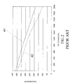
- such a known laminated inductor shows a rapid lowering curve of inductance, as indicated by curve 42 shown in FIG. 2 , for applications of higher than 1,200 mA (a large current), so that the applications thereof are limited. Thus, further improvement is desired.
- the present invention is thus made to overcome the above discussed problems by providing a laminated inductor with enhanced current endurance.
- the primary purpose of the present invention is to provide a laminated inductor with enhanced current endurance, which comprises the following constituent components:
- a plurality of magentic plates is stacked sequentially to form the laminated inductor.
- the laminated inductor has opposite ends that are respectively mounted to electrode contacts.
- Each of the magentic plates comprises a magnetic plate, which has moderate magnetic permeability.
- the moderate-permeability magnetic plate shows a value of magnetic permeability ( ⁇ i) in the range of 60-300 for a frequency below 100 MHz.
- the magentic plates are printed with conductor patterns and form through holes.
- each of the magentic plates is provided, on a surface thereof, with a magnetic body having high permeability.
- the high-permeability magnetic body shows a value of magnetic permeability ( ⁇ i) in the range of 400-1,000 for a frequency below 100 MHz.
- the topmost magentic plate of the stacked magentic plates is provided with a conductive terminal.
- At least one spacer assembly is interposed between the magentic plates.
- the spacer assembly is formed of two magnetic plates having moderate magnetic permeability interposing therebetween a magnetic plate having low permeability.
- the low-permeability magnetic plate shows a value of magnetic permeability ( ⁇ i) in the range of 1-30 for a frequency below 100 MHz.
- the moderate-permeability magnetic plates of the spacer assembly are each provided with a high-permeability magnetic body, and the moderate-permeability magnetic plates each form a through hole.
- the low-permeability magnetic plate of the spacer assembly is provided with a high-permeability magnetic body and forms a through hole.
- a magnetic top lid is set on and covers an outside surface of the topmost one of the magentic plates.
- the magnetic top lid is of high magnetic permeability and the high-permeability magnetic lid shows a value of magnetic permeability ( ⁇ i) in the range of 400-1,000 for a frequency below 100 MHz.
- a magnetic bottom lid is stacked on an outside surface of a bottomost one of the magentic plates.
- the magnetic bottom lid is of high magnetic permeability and the high-permeability magnetic bottom lid shows a value of magnetic permeability ( ⁇ i) in the range of 400-1,000 for a frequency below 100 MHz.
- the magnetic bottom lid is printed with a conductor pattern.
- the magnetic bottom lid is provided with a conductive terminal.
- the magnetic bottom lid and the magnetic top lid are arranged to interpose therebetween the plurality of sequentially stacked magentic plates and the at least one spacer assembly to construct the laminated inductor with the opposite ends of the laminated inductor being respectively coupled to the electrode contacts.
- the DC (direct current) superimposition characteristics of the laminated inductor according to the present invention is significantly improved, allowing for wide applications of the laminated inductor of the present invention and thus realizing a laminated inductor with enhanced current endurance.
- FIG. 1 is an exploded view showing a conventional laminated inductor.
- FIG. 2 is a plot showing characteristics curves of a conventional laminated inductor and a laminated inductor according to the present invention.
- FIG. 3 is an exploded view of a laminated inductor according to the present invention.
- FIG. 4 is a perspective view showing the laminated inductor according to the present invention.
- FIG. 5 is a top plan view of the laminated inductor according to the present invention.
- FIG. 6 is a schematic view illustrating the arrangement of each layer of the laminated inductor according to the present invention.
- the present invention provides a laminated inductor that shows enhanced current endurance.
- the laminated inductor of the present invention comprises the following components.
- a plurality of magentic plates 11 is stacked sequentially to form the laminated inductor, which is generally designated at 1 , as shown in FIG. 4 .
- the laminated inductor 1 has opposite ends that are respectively mounted to two electrode contacts 14 .
- Each of the magentic plates 11 comprises a magnetic plate, which has moderate magnetic permeability and will be referred to as moderate-permeability magnetic plate hereinafter.
- the moderate-permeability magnetic plate shows a value of magnetic permeability ( ⁇ i) in the range of 60-300 for a frequency below 100 MHz.
- the magentic plates 11 are printed with conductor patterns 12 . Further, the magentic plates 11 are provided with through holes 13 .
- each of the magentic plates 11 is provided, on a surface thereof, with a magnetic body 5 having high permeability, which will be referred to as high-permeability magentic body hereinafter.
- the high-permeability magnetic body 5 shows a value of magnetic permeability ( ⁇ i) in the range of 400-1,000 for a frequency below 100 MHz.
- the topmost magentic plate 11 of the plurality of stacked magentic plates 11 is provided with a conductive terminal 43 , which is in electrical connection with a respective electrode contact 14 of the laminated inductor 1 .
- At least one spacer assembly 2 is interposed between the magentic plates 11 .
- the spacer assembly 2 is formed of two magnetic plates 21 having moderate magnetic permeability (which will be referred to as moderate-permeability magnetic plates hereinafter) interposing therebetween a magnetic plate 22 having low permeability (which will be referred to as low-permeability magnetic plate hereinafter).
- the low-permeability magnetic plate 22 shows a value of magnetic permeability ( ⁇ i) in the range of 1-30 for a frequency below 100 MHz.
- the moderate-permeability magnetic plates 21 of the spacer assembly 2 are each provided with a high-permeability magnetic body 5 , and the moderate-permeability magnetic plates 21 each form a through hole 13 .
- the low-permeability magnetic plate 22 of the spacer assembly 2 is provided with a high-permeability magnetic body 5 , and the low-permeability magnetic plate 22 forms a through hole 13 .
- a magnetic top lid 3 is set on and covers an outside surface of the topmost one of the magentic plates 11 .
- the magnetic top lid 3 is of high magnetic permeability and the high-permeability magnetic lid shows a value of magnetic permeability ( ⁇ i) in the range of 400-1,000 for a frequency below 100 MHz.
- a magnetic bottom lid 15 is stacked on an outside surface of a bottomost one of the magentic plates 11 .
- the magnetic bottom lid 15 is of high magnetic permeability and the high-permeability magnetic bottom lid shows a value of magnetic permeability ( ⁇ i) in the range of 400-1,000 for a frequency below 100 MHz.
- the magnetic bottom lid 15 is printed with a conductor pattern 12 and the magnetic bottom lid 15 is provided with a conductive terminal 43 .
- the magnetic bottom lid 15 and the magnetic top lid 3 are arranged to interpose therebetween the plurality of sequentially stacked magentic plates 11 and the at least one spacer assembly 2 to construct the laminated inductor 1 with the opposite ends of the laminated inductor 1 being respectively coupled to the electrode contacts 14 .
- the conductor pattern 12 of the magnetic bottom lid 15 and the conductor patterns 12 of the plurality of magentic plates 11 can be set in electrical connection with each other. Due to the electrical connection formed between adjacent conductor patterns 12 , the inter-connected conductor patterns construct a helically arranged coil 4 , as shown in FIG. 5 , with opposite ends of the coil 4 being constituted by the two terminals 43 , which are respectively set in electrical connection with the electrode contacts 14 mounted to the opposite ends of the laminated inductor 1 .
- each of the magentic plates 11 being provided on a surface thereof with a high-permeability magnetic body 5 , and further due to the arrangement of the spacer assembly 2 , DC (direct current) superimposition characteristics of the laminated inductor 1 is significantly improved, whereby the laminated inductor 1 of the present invention shows a gently lowering curve of inductance as indicated by curve 41 shown in FIG. 2 , when used in a large current application.
- This allows for wide applications of the laminated inductor 1 of the present invention to thereby realize a laminated inductor with enhanced current endurance.
Landscapes
- Engineering & Computer Science (AREA)
- Power Engineering (AREA)
- Microelectronics & Electronic Packaging (AREA)
- Coils Or Transformers For Communication (AREA)
Applications Claiming Priority (3)
| Application Number | Priority Date | Filing Date | Title |
|---|---|---|---|
| TW98207913U | 2009-05-08 | ||
| TW098207913U TWM365534U (en) | 2009-05-08 | 2009-05-08 | Improved laminated inductor sustainable to large current |
| TW098207913 | 2009-08-05 |
Publications (2)
| Publication Number | Publication Date |
|---|---|
| US20110032066A1 US20110032066A1 (en) | 2011-02-10 |
| US8093981B2 true US8093981B2 (en) | 2012-01-10 |
Family
ID=43534393
Family Applications (1)
| Application Number | Title | Priority Date | Filing Date |
|---|---|---|---|
| US12/712,129 Expired - Fee Related US8093981B2 (en) | 2009-05-08 | 2010-02-24 | Laminated inductor with enhanced current endurance |
Country Status (2)
| Country | Link |
|---|---|
| US (1) | US8093981B2 (zh) |
| TW (1) | TWM365534U (zh) |
Cited By (8)
| Publication number | Priority date | Publication date | Assignee | Title |
|---|---|---|---|---|
| US20130200979A1 (en) * | 2012-02-08 | 2013-08-08 | Taiyo Yuden Co., Ltd. | Laminated inductor |
| US8669839B2 (en) | 2012-02-08 | 2014-03-11 | Taiyo Yuden Co., Ltd. | Laminated inductor |
| US20160293316A1 (en) * | 2015-04-01 | 2016-10-06 | Samsung Electro-Mechanics Co., Ltd. | Coil electronic component and method of manufacturing the same |
| US10396144B2 (en) | 2017-04-24 | 2019-08-27 | International Business Machines Corporation | Magnetic inductor stack including magnetic materials having multiple permeabilities |
| US10593449B2 (en) | 2017-03-30 | 2020-03-17 | International Business Machines Corporation | Magnetic inductor with multiple magnetic layer thicknesses |
| US10597769B2 (en) | 2017-04-05 | 2020-03-24 | International Business Machines Corporation | Method of fabricating a magnetic stack arrangement of a laminated magnetic inductor |
| US10607759B2 (en) | 2017-03-31 | 2020-03-31 | International Business Machines Corporation | Method of fabricating a laminated stack of magnetic inductor |
| US11170933B2 (en) | 2017-05-19 | 2021-11-09 | International Business Machines Corporation | Stress management scheme for fabricating thick magnetic films of an inductor yoke arrangement |
Families Citing this family (3)
| Publication number | Priority date | Publication date | Assignee | Title |
|---|---|---|---|---|
| KR101523872B1 (ko) * | 2011-10-14 | 2015-05-28 | 가부시키가이샤 무라타 세이사쿠쇼 | 전자 부품 |
| JP6534880B2 (ja) * | 2015-07-14 | 2019-06-26 | 太陽誘電株式会社 | インダクタ及びプリント基板 |
| JP2019096818A (ja) * | 2017-11-27 | 2019-06-20 | 株式会社村田製作所 | 積層型コイル部品 |
Citations (10)
| Publication number | Priority date | Publication date | Assignee | Title |
|---|---|---|---|---|
| US6264777B1 (en) * | 1997-02-28 | 2001-07-24 | Taiyo Yuden Co., Ltd. | Laminated composite electronic device and a manufacturing method thereof |
| US7304557B2 (en) * | 2004-06-07 | 2007-12-04 | Murata Manufacturing Co., Ltd. | Laminated coil |
| US7453343B2 (en) * | 2003-02-26 | 2008-11-18 | Tdk Corporation | Thin-film type common-mode choke coil |
| US7719398B2 (en) * | 2005-01-07 | 2010-05-18 | Murata Manufacturing Co., Ltd. | Laminated coil |
| US7719399B2 (en) * | 2006-06-20 | 2010-05-18 | Murata Manufacturing Co., Ltd. | Laminated coil component |
| US7817007B2 (en) * | 2007-08-20 | 2010-10-19 | Sumitomo Electro-Mechanics Co., Ltd. | Laminated inductor |
| US7839735B2 (en) * | 2006-07-14 | 2010-11-23 | Sony Corporation | Phase difference detection apparatus, phase difference detection method, reproduction apparatus and tracking controlling method |
| US7907044B2 (en) * | 2006-01-31 | 2011-03-15 | Hitachi Metals, Ltd. | Laminate device and module comprising same |
| US7994889B2 (en) * | 2006-06-01 | 2011-08-09 | Taiyo Yuden Co., Ltd. | Multilayer inductor |
| US8004381B2 (en) * | 2006-07-05 | 2011-08-23 | Hitachi Metals, Ltd. | Laminated device |
-
2009
- 2009-05-08 TW TW098207913U patent/TWM365534U/zh not_active IP Right Cessation
-
2010
- 2010-02-24 US US12/712,129 patent/US8093981B2/en not_active Expired - Fee Related
Patent Citations (10)
| Publication number | Priority date | Publication date | Assignee | Title |
|---|---|---|---|---|
| US6264777B1 (en) * | 1997-02-28 | 2001-07-24 | Taiyo Yuden Co., Ltd. | Laminated composite electronic device and a manufacturing method thereof |
| US7453343B2 (en) * | 2003-02-26 | 2008-11-18 | Tdk Corporation | Thin-film type common-mode choke coil |
| US7304557B2 (en) * | 2004-06-07 | 2007-12-04 | Murata Manufacturing Co., Ltd. | Laminated coil |
| US7719398B2 (en) * | 2005-01-07 | 2010-05-18 | Murata Manufacturing Co., Ltd. | Laminated coil |
| US7907044B2 (en) * | 2006-01-31 | 2011-03-15 | Hitachi Metals, Ltd. | Laminate device and module comprising same |
| US7994889B2 (en) * | 2006-06-01 | 2011-08-09 | Taiyo Yuden Co., Ltd. | Multilayer inductor |
| US7719399B2 (en) * | 2006-06-20 | 2010-05-18 | Murata Manufacturing Co., Ltd. | Laminated coil component |
| US8004381B2 (en) * | 2006-07-05 | 2011-08-23 | Hitachi Metals, Ltd. | Laminated device |
| US7839735B2 (en) * | 2006-07-14 | 2010-11-23 | Sony Corporation | Phase difference detection apparatus, phase difference detection method, reproduction apparatus and tracking controlling method |
| US7817007B2 (en) * | 2007-08-20 | 2010-10-19 | Sumitomo Electro-Mechanics Co., Ltd. | Laminated inductor |
Cited By (14)
| Publication number | Priority date | Publication date | Assignee | Title |
|---|---|---|---|---|
| US20130200979A1 (en) * | 2012-02-08 | 2013-08-08 | Taiyo Yuden Co., Ltd. | Laminated inductor |
| US8669839B2 (en) | 2012-02-08 | 2014-03-11 | Taiyo Yuden Co., Ltd. | Laminated inductor |
| US9007160B2 (en) * | 2012-02-08 | 2015-04-14 | Taiyo Yuden Co., Ltd. | Laminated inductor |
| US20160293316A1 (en) * | 2015-04-01 | 2016-10-06 | Samsung Electro-Mechanics Co., Ltd. | Coil electronic component and method of manufacturing the same |
| US10593450B2 (en) | 2017-03-30 | 2020-03-17 | International Business Machines Corporation | Magnetic inductor with multiple magnetic layer thicknesses |
| US10593449B2 (en) | 2017-03-30 | 2020-03-17 | International Business Machines Corporation | Magnetic inductor with multiple magnetic layer thicknesses |
| US11361889B2 (en) | 2017-03-30 | 2022-06-14 | International Business Machines Corporation | Magnetic inductor with multiple magnetic layer thicknesses |
| US10607759B2 (en) | 2017-03-31 | 2020-03-31 | International Business Machines Corporation | Method of fabricating a laminated stack of magnetic inductor |
| US11222742B2 (en) | 2017-03-31 | 2022-01-11 | International Business Machines Corporation | Magnetic inductor with shape anisotrophy |
| US10597769B2 (en) | 2017-04-05 | 2020-03-24 | International Business Machines Corporation | Method of fabricating a magnetic stack arrangement of a laminated magnetic inductor |
| US11479845B2 (en) | 2017-04-05 | 2022-10-25 | International Business Machines Corporation | Laminated magnetic inductor stack with high frequency peak quality factor |
| US10396144B2 (en) | 2017-04-24 | 2019-08-27 | International Business Machines Corporation | Magnetic inductor stack including magnetic materials having multiple permeabilities |
| US11170933B2 (en) | 2017-05-19 | 2021-11-09 | International Business Machines Corporation | Stress management scheme for fabricating thick magnetic films of an inductor yoke arrangement |
| US11367569B2 (en) | 2017-05-19 | 2022-06-21 | International Business Machines Corporation | Stress management for thick magnetic film inductors |
Also Published As
| Publication number | Publication date |
|---|---|
| TWM365534U (en) | 2009-09-21 |
| US20110032066A1 (en) | 2011-02-10 |
Similar Documents
| Publication | Publication Date | Title |
|---|---|---|
| US8093981B2 (en) | Laminated inductor with enhanced current endurance | |
| US9607753B2 (en) | Multilayer inductor | |
| US11217372B2 (en) | Coil component | |
| US6483414B2 (en) | Method of manufacturing multilayer-type chip inductors | |
| JP2001044037A (ja) | 積層インダクタ | |
| US20130214888A1 (en) | Laminated inductor | |
| JP2001044036A (ja) | 積層インダクタ | |
| US11011291B2 (en) | Laminated electronic component | |
| KR101565705B1 (ko) | 인덕터 | |
| US11887764B2 (en) | Laminated electronic component | |
| WO2012144103A1 (ja) | 積層型インダクタ素子及び製造方法 | |
| KR101338139B1 (ko) | 파워 인덕터 | |
| JP2002270432A (ja) | 積層部品及びその製造方法 | |
| KR102064104B1 (ko) | 적층형 전자부품 어레이 및 그 제조방법 | |
| JPH07163146A (ja) | Dc−dcコンバータ | |
| US20120161914A1 (en) | Transformer | |
| JP4724940B2 (ja) | 積層型インダクタンス素子及び積層型インダクタンス素子の製造方法 | |
| US9570227B1 (en) | Magnetic excitation coil structure | |
| KR20190014727A (ko) | 듀얼 코어 평면 트랜스포머 | |
| KR101004878B1 (ko) | 적층형 인덕터 | |
| KR101946260B1 (ko) | 적층형 전자부품 어레이 및 그 제조방법 | |
| JP2007281379A (ja) | 積層インダクタ | |
| KR20000040049A (ko) | 적층형 칩 인덕터 | |
| KR20070108726A (ko) | 표면 실장형 칩 타입 전자 부품 및 적층 시트 | |
| KR20190099834A (ko) | 코일 전자 부품 |
Legal Events
| Date | Code | Title | Description |
|---|---|---|---|
| AS | Assignment |
Owner name: MAG. LAYERS SCIENTIFIC-TECHNICS CO., LTD., TAIWAN Free format text: ASSIGNMENT OF ASSIGNORS INTEREST;ASSIGNOR:CHUNG, JUI-MIN;REEL/FRAME:023987/0279 Effective date: 20100224 |
|
| ZAAA | Notice of allowance and fees due |
Free format text: ORIGINAL CODE: NOA |
|
| ZAAB | Notice of allowance mailed |
Free format text: ORIGINAL CODE: MN/=. |
|
| STCF | Information on status: patent grant |
Free format text: PATENTED CASE |
|
| FPAY | Fee payment |
Year of fee payment: 4 |
|
| MAFP | Maintenance fee payment |
Free format text: PAYMENT OF MAINTENANCE FEE, 8TH YR, SMALL ENTITY (ORIGINAL EVENT CODE: M2552); ENTITY STATUS OF PATENT OWNER: SMALL ENTITY Year of fee payment: 8 |
|
| FEPP | Fee payment procedure |
Free format text: MAINTENANCE FEE REMINDER MAILED (ORIGINAL EVENT CODE: REM.); ENTITY STATUS OF PATENT OWNER: SMALL ENTITY |
|
| LAPS | Lapse for failure to pay maintenance fees |
Free format text: PATENT EXPIRED FOR FAILURE TO PAY MAINTENANCE FEES (ORIGINAL EVENT CODE: EXP.); ENTITY STATUS OF PATENT OWNER: SMALL ENTITY |
|
| STCH | Information on status: patent discontinuation |
Free format text: PATENT EXPIRED DUE TO NONPAYMENT OF MAINTENANCE FEES UNDER 37 CFR 1.362 |
|
| FP | Lapsed due to failure to pay maintenance fee |
Effective date: 20240110 |