US8089134B2 - Semiconductor device - Google Patents
Semiconductor device Download PDFInfo
- Publication number
- US8089134B2 US8089134B2 US12/320,666 US32066609A US8089134B2 US 8089134 B2 US8089134 B2 US 8089134B2 US 32066609 A US32066609 A US 32066609A US 8089134 B2 US8089134 B2 US 8089134B2
- Authority
- US
- United States
- Prior art keywords
- semiconductor
- region
- semiconductor device
- semiconductor region
- cathode
- Prior art date
- Legal status (The legal status is an assumption and is not a legal conclusion. Google has not performed a legal analysis and makes no representation as to the accuracy of the status listed.)
- Expired - Fee Related, expires
Links
Images


Classifications
-
- H—ELECTRICITY
- H10—SEMICONDUCTOR DEVICES; ELECTRIC SOLID-STATE DEVICES NOT OTHERWISE PROVIDED FOR
- H10D—INORGANIC ELECTRIC SEMICONDUCTOR DEVICES
- H10D89/00—Aspects of integrated devices not covered by groups H10D84/00 - H10D88/00
- H10D89/60—Integrated devices comprising arrangements for electrical or thermal protection, e.g. protection circuits against electrostatic discharge [ESD]
- H10D89/601—Integrated devices comprising arrangements for electrical or thermal protection, e.g. protection circuits against electrostatic discharge [ESD] for devices having insulated gate electrodes, e.g. for IGFETs or IGBTs
- H10D89/611—Integrated devices comprising arrangements for electrical or thermal protection, e.g. protection circuits against electrostatic discharge [ESD] for devices having insulated gate electrodes, e.g. for IGFETs or IGBTs using diodes as protective elements
Definitions
- the present invention relates to a semiconductor device equipped with a primary semiconductor element and a temperature detecting element.
- a semiconductor device used for power switching is provided with an overheat protection function to prevent thermal breakdown of the semiconductor device due to an over-current.
- a function using change of forward and reverse characteristics of a diode in accordance with temperature is commonly known as the overheat protection function.
- the forward voltage and the saturation voltage of a diode vary substantially linearly in accordance with temperature. Therefore, when a semiconductor device and a diode are provided as a main element (hereinafter referred to as primary semiconductor element) and a temperature detecting element respectively, the temperature of the primary semiconductor element can be detected by monitoring the forward voltage or the saturation voltage of the diode (e.g. as disclosed in U.S. Pat. No.
- FIG. 1 is a sectional view showing the configuration of a semiconductor device according to the related art.
- the semiconductor device according to the related art has an N ⁇ drift layer 3 , a surface structure of a primary semiconductor element 1 , and a temperature detecting diode 2 .
- the surface structure of the primary semiconductor element 1 and the temperature detecting diode 2 are provided in a first principal surface of the N ⁇ drift layer 3 .
- the surface structure of the primary semiconductor element 1 has a P-base region 4 a , an N + emitter (source) region 5 , a gate insulating film 6 , a gate electrode 7 , and an emitter (source) electrode 8 .
- the temperature detecting element 2 has a P-type anode region (a P-base region 4 b and a P + region 9 ), an N + cathode region 10 , an anode electrode (not shown), and a cathode electrode (not shown).
- a semiconductor device having a primary semiconductor element 1 , an insulating film 11 formed in a first principal surface of a constituent semiconductor member of the primary semiconductor element 1 , and a temperature detecting diode 2 formed on the insulating film 11 is commonly known as represented by a semiconductor device shown in FIG. 2 (e.g. as shown in Japanese patent document JP-A-6-117942).
- a power module in which a thermistor for detecting heat emitted from a switching circuit and a rectifier circuit is disposed nearby the switching circuit and the rectifier circuit is commonly known (e.g. as shown in Japanese patent document JP-A-2005-286270).
- a parasitic diode is however formed from the anode region of the temperature detecting diode and the N ⁇ drift layer.
- a current flowing in the channel also flows in the parasitic diode. For this reason, there is a problem that the forward voltage or the saturation voltage of the temperature detecting diode varies according to whether the primary semiconductor element is in an ON state or in an OFF state.
- the primary semiconductor element is an IGBT (Insulated Gate Bipolar Transistor)
- a parasitic thyristor is formed from a P collector layer in a second principal surface, the N ⁇ drift layer and the P-type anode region and N + cathode region of the temperature detecting diode.
- this IGBT is turned OFF, there is a risk that latch-up breakdown will be caused by malfunction of the parasitic thyristor because holes which are minority carriers are imported from the N ⁇ drift layer into the anode region.
- an object of the invention is to provide a semiconductor device equipped with a temperature detecting element having constant temperature characteristic regardless of the state of a primary semiconductor element.
- a further object of the invention is to provide a semiconductor device high in temperature detection accuracy.
- the semiconductor device is equipped with a primary semiconductor element and a temperature detecting element for detecting a temperature of the primary semiconductor element.
- the semiconductor device includes a first semiconductor layer of a first conductivity type which forms the primary semiconductor element, a second semiconductor region of a second conductivity type provided in the first semiconductor layer, and a third semiconductor region of the first conductivity type provided in the second semiconductor region, where the temperature detecting element is provided in the third semiconductor region and is separated from the first semiconductor layer by a PN junction.
- FIG. 2 is a sectional view showing another example of the configuration of the semiconductor device according to the related art.
- FIG. 3 is a sectional view showing the configuration of a semiconductor device according to Embodiment 1 of the invention.
- FIG. 5 is a sectional view showing the configuration of a semiconductor device according to Embodiment 3 of the invention.
- FIG. 8 is a plan view showing an example of the planar layout of the semiconductor device according to Embodiment 5 of the invention.
- FIG. 10 is a sectional view showing the configuration of a semiconductor device according to Embodiment 6 of the invention.
- FIG. 12 is a plan view showing an example of the planar layout of the semiconductor device according to Embodiment 7 of the invention.
- FIG. 17 is a sectional view showing the configuration of a semiconductor device according to Embodiment 10 of the invention.
- FIG. 18 is a sectional view showing the configuration of a semiconductor device according to Embodiment 11 of the invention.
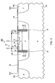
- FIG. 3 is a sectional view showing the configuration of a semiconductor device according to Embodiment 1 of the invention.
- the semiconductor device 100 has a first P well 24 b provided as a second semiconductor region in a first principal surface of an N ⁇ drift layer 23 which is a first semiconductor layer.
- An N well 25 which is a third semiconductor region is provided in the first P well 24 b .
- a temperature detecting diode (temperature detecting element) 22 is provided in the N well 25 .
- a high-concentration P + anode region 26 as a fourth semiconductor region and a high-concentration N + cathode contact region 27 are provided in the N well 25 .
- An anode electrode (A) is connected to the P + anode region 26 .
- a cathode electrode (K) is connected to the N + cathode contact region 27 .
- the N + cathode contact region 27 is provided to bring the cathode electrode into low resistance contact with the N well 25 which serves as a cathode region.
- the semiconductor device 100 is further equipped with a primary semiconductor element which is not shown but formed from the N ⁇ drift layer 23 .
- the temperature detecting diode 22 is separated from the not-shown primary semiconductor element by a PN junction between the first P well 24 b and the N well 25 .
- the first P well 24 b is sufficiently high in concentration to prevent latch-up breakdown due to a parasitic thyristor. In addition, the first P well 24 b is sufficiently deep to prevent latch-up breakdown due to the parasitic thyristor.
- a side of the N well 25 is surrounded by a P + high-concentration region 28 that is a fifth semiconductor region.
- the P + high-concentration region 28 is higher in concentration than the first P well 24 b .
- the P + high-concentration region 28 is covered with an insulating film 29 .
- the first P well 24 b and the P + high-concentration region 28 are electrically floating.
- a second P well 24 c is provided outside the first P well 24 b so as to be separated from the first P well 24 b .
- the second P well 24 c is set to have the same electric potential as that of an emitter (source) of the not-shown primary semiconductor element, so that the second P well 24 c forms a diverter for extracting holes.
- the planar layout of the semiconductor device 100 is not shown but shaped like concentric circles with the P + anode region 26 as their center.
- the first P well 24 b may be formed at the same time that a guard ring not shown is formed.
- the P + anode region 26 may be formed at the same time that a P + contact region for bringing an electrode into low resistance contact with a P-type semiconductor region of the primary semiconductor device is formed.
- the N + cathode contact region 27 may be formed at the same time that an N + contact region or an N + emitter (source) region for bringing an electrode into low resistance contact with an N-type semiconductor region of the primary semiconductor element is formed.
- the production process of the semiconductor device 100 can be simplified. When these three steps are all used for production of the semiconductor device 100 , the production process can be simplified remarkably compared with production of the related-art semiconductor device shown in FIG. 2 , because only addition of a process of forming the N well 25 is required.
- Embodiment 1 even when a channel is formed in the primary semiconductor element and a current flows in the channel, there is no influence on the saturation voltage of the temperature detecting diode 22 because the temperature detecting diode 22 is separated from the primary semiconductor element by a junction. That is, it is possible to produce a temperature detecting diode 22 having a constant saturation voltage regardless of the state of the primary semiconductor element because the saturation voltage of the temperature detecting diode 22 can be prevented from varying according to the state of the primary semiconductor element. In addition, it is possible to produce a semiconductor device 100 equipped with such a temperature detecting diode 22 .
- the response speed of the primary semiconductor element to temperature change is high.
- the P + anode region 26 and the N + cathode contact region 27 may be brought into contact with each other. In this manner, variation in the ON-voltage can be reduced.
- FIG. 4 is a sectional view showing the configuration of a semiconductor device according to Embodiment 2 of the invention.
- the semiconductor device 200 is configured in the same manner as the semiconductor device 100 according to Embodiment 1 shown in FIG. 3 except that a side of the N well 25 is surrounded by a trench gate structure 31 in place of the P + high concentration region 28 . Occurrence of latch-up in the transverse direction can be prevented because activation of a transverse NPN transistor can be completely prevented by this trench gate structure 31 .
- the trench gate structure 31 is provided in a terminal portion of the N well 25 in the first P well 24 b .
- the trench gate structure 31 extends to be deeper than the N well 25 .
- An insulating film 32 such as an oxide film is provided in a portion being in contact with a semiconductor of the trench gate structure 31 , i.e. in an inner circumferential surface of the trench.
- the inside of the insulating film 32 is filled with a conductor such as polysilicon 33 . It is preferable that this polysilicon 33 is set to have the same electric potential as that of the cathode.
- the gate structure of the primary semiconductor element is a trench gate structure
- the trench gate structure 31 may be formed at the same time that the trench gate structure of the primary semiconductor element is formed.
- the remaining configuration is the same as in Embodiment 1.
- the first P well 24 b has the same electric potential as the emitter (source) potential. As a result, occurrence of latchup due to high dV/dt can be suppressed because voltage change (dV/dt) at the time of switching becomes gentle.
- the hole extraction region 42 may be formed by another P well provided separately from the first P well 24 b .
- the P well forming the hole extraction region 42 may be set to have the same electric potential as the emitter (source) potential of the primary semiconductor element 21 and the first P well 24 b may be electrically floating in the same manner as in Embodiment 1.
- the hole extraction region 42 may be formed by the same P-base region as that of the primary semiconductor element 21 and the P-base region may be set to have the same electric potential as the emitter (source) potential.
- the primary semiconductor element 21 is not particularly limited. Examples of the primary semiconductor element 21 include a vertical IGBT with a planar gate structure, a vertical MOSFET (Metal Oxide Semiconductor Field Effect Transistor) with a planar gate structure, etc.
- a P collector region 46 and a collector electrode 47 are provided in a second principal surface of the N ⁇ drift layer 23 .
- an N drain region 48 and a drain electrode 49 are provided in the second principal surface of the N ⁇ drift layer 23 .
- the second principal surface side structure of the N ⁇ drift layer 23 is also applied to Embodiments 4 to 6.
- FIG. 6 is a sectional view showing the configuration of a semiconductor device according to Embodiment 4 of the invention.
- the semiconductor device 400 is a device including the temperature detecting diode 22 configured as shown in FIG. 4 and its peripheral structure.
- the temperature detecting diode 22 configured as shown in FIG. 4 is suitable for the case where the gate structure of the primary semiconductor element 21 is a trench gate structure 51 , because a trench gate structure 31 is provided in a terminal portion of the N well 25 .
- the trench gate structure 31 of the temperature detecting diode 22 can be formed at the same time that the trench gate structure 51 of the primary semiconductor element 21 is formed.
- the hole extraction region 42 of the diverter 41 is formed by a P-base region.
- the hole extraction region 42 has a high-concentration P + contact region 43 in its front surface and is set to have the same electric potential as the emitter (source) potential of the primary semiconductor element 21 .
- the first P well 24 b may be electrically floating and may be set to have the same electric potential as the emitter (source) potential of the primary semiconductor element 21 .
- FIG. 7 is a sectional view showing the configuration of a semiconductor device according to Embodiment 5 of the invention.
- FIG. 8 is a plan view showing an example of the planar layout of the semiconductor device according to Embodiment 5.
- the semiconductor device 500 is configured in the same manner as the semiconductor device 400 according to Embodiment 4 shown in FIG. 6 except that the hole extraction region 42 of the diverter 41 is formed by another P well provided separately from the first P well 24 b .
- a high-concentration P + contact region 43 is provided in a front surface of the P well serving as the hole extraction region 42 and the hole extraction region 42 is set to have the same electric potential as the emitter (source) potential of the primary semiconductor device 21 .
- the first P well 24 b may be electrically floating and may be set to have the same electric potential as the emitter (source) potential of the primary semiconductor element 21 .
- FIG. 9 is a plan view showing another example of the planar layout of the semiconductor device according to Embodiment 5.
- the planar layout shown in FIG. 9 is a layout in which a plurality of temperature detecting diodes 22 , for example, four temperature detecting diodes 22 are provided though the number of temperature detecting diodes 22 is not particularly limited. As shown in FIG. 9 , four temperature detecting diodes 22 are arranged side by side and a hole extraction region 42 of a diverter is provided to surround the four temperature detecting diodes 22 .
- FIG. 10 is a sectional view showing the configuration of a semiconductor device according to Embodiment 6 of the invention.
- the semiconductor device 600 is configured in the same manner as the semiconductor device 500 according to Embodiment 5 shown in FIG. 7 except that the first P well 24 b extends in the transverse direction to form a hole extraction region 42 of a diverter 41 in the same manner as in Embodiment 3. This is equivalent to formation of the first P well 24 b and the hole extraction region 42 with one and the same pattern.
- a primary semiconductor element with a trench gate structure and a temperature detecting diode without any trench gate structure, such as the temperature detecting diode 22 configured as shown in FIG. 3 may be combined in Embodiments 4 to 6.
- FIG. 11 is a sectional view showing the configuration of a semiconductor device according to Embodiment 7 of the invention.
- the semiconductor device 100 has a first P well 24 b provided as a second semiconductor region in a first principal surface of an N drift layer 23 which is a first semiconductor layer.
- An N well 25 which is a third semiconductor region is provided in the first P well 24 b .
- a temperature detecting diode (temperature detecting element) 22 is provided in the N well 25 .
- a high-concentration P + anode region 26 as a fourth semiconductor region is provided in the N well 25 .
- a high-concentration N + cathode contact region 27 as a fifth semiconductor region is provided in the P + anode region 26 .
- An anode electrode (A) 28 is in contact with the P + anode region 26 and the N well 25 . That is, the P + anode region 26 and the N well 25 are short-circuited by the anode electrode 28 .
- a cathode electrode (K) 29 is in contact with the N + cathode contact region 27 .
- the first P well 24 b is sufficiently high in concentration to prevent latch-up breakdown due to a parasitic thyristor.
- the first P well 24 b is sufficiently deep to prevent latch-up breakdown due to the parasitic thyristor.
- the first P well 24 b is covered with an insulating film 30 and is electrically floating. That is, the semiconductor device 100 is further equipped with a primary semiconductor element which is not shown but formed from the N ⁇ drift layer 23 .
- the first P well 24 b is not connected to any of the electrodes of the primary semiconductor element.
- the temperature detecting diode 22 is separated from the not-shown primary semiconductor element by a PN junction between the first P well 24 b and the N well 25 .
- a second P well 24 c is provided outside the first P well 24 b so as to be separated from the first P well 24 b .
- the second P well 24 c forms a diverter for extracting holes.
- a hole extraction electrode 31 is in contact with the second P well 24 c .
- the same electric potential as that of an emitter (source) of the not-shown primary semiconductor element is applied to the second P well 24 c through the hole extraction electrode 31 .
- a P collector region 36 and a collector electrode 37 are provided in a second principal surface of the N ⁇ drift layer 23 .
- an N drain region 38 and a drain electrode 39 are provided in the second principal surface of the N ⁇ drift layer 23 .
- FIG. 12 is a plan view showing an example of the planar layout of the semiconductor device according to Embodiment 7.
- the planar layout of the semiconductor device 100 is shaped like concentric circles with the N + cathode region 27 as their center.
- FIG. 13 shows the planar layout in the case where a plurality of temperature detecting diodes 22 , for example, three temperature detecting diodes 22 are provided though the number of temperature detecting diodes 22 is not particularly limited.
- three temperature detecting diodes 22 are arranged side by side and the second P well 24 c is provided to surround the three temperature detecting diodes 22 .
- the first P well 24 b may be formed at the same time that a P-type field limiting ring or P-type RESURF (reduced surface field) layer of a withstand pressure structure portion of the not-shown primary semiconductor element is formed.
- the production process of the semiconductor device 100 can be simplified because it is not necessary to form the first P well 24 b separately from the primary semiconductor element.
- the P + anode region 26 may be formed at the same time that a P + body region of the primary semiconductor device is formed.
- the N + cathode contact region 27 may be formed at the same time that an N + emitter (source) region of the primary semiconductor element is formed. In this manner, the production process of the semiconductor device 100 can be further simplified because it is not necessary to form the P + anode region 26 and the N + cathode contact region 27 separately from the primary semiconductor element.
- the first P well 24 b and the N well 25 may be formed at the same time that the P-type field limiting ring or P-type RESURF layer is formed.
- the temperature detecting diode 22 can be produced in the production process of the primary semiconductor element without addition of any special process. Accordingly, the production process can be simplified remarkably compared with production of the related-art semiconductor device shown in FIG. 2 .
- boron can be used as the ionic species for formation of the P-type region
- arsenic can be used as the ionic species for formation of the N-type region.
- Embodiment 7 even when a channel is formed in the primary semiconductor element and a current flows in the channel, there is no influence on the forward voltage of the temperature detecting diode 22 because the temperature detecting diode 22 is separated from the primary semiconductor element by a junction. That is, it is possible to produce a temperature detecting diode 22 having a constant forward voltage regardless of the state of the primary semiconductor element because the forward voltage of the temperature detecting diode 22 can be prevented from varying according to the state of the primary semiconductor element. In addition, it is possible to produce a semiconductor device 100 equipped with such a temperature detecting diode 22 .
- activation of a parasitic thyristor can be suppressed by the first P well 24 b .
- activation of the parasitic thyristor can be suppressed by surrounding the temperature detecting diode 22 with the second P well 24 c which is the hole extraction region.
- activation of the parasitic thyristor can be suppressed by short-circuiting between the N well 25 and the P + anode region 26 . Accordingly, it is possible to suppress latch-up breakdown due to the parasitic thyristor so that it is possible to produce a semiconductor device 100 high in latch-up tolerance.
- the primary semiconductor element can be operated more stably compared with the configuration in which the temperature detecting diode 22 is simply electrically insulated and separated from the primary semiconductor element.
- the response speed of the primary semiconductor element to temperature change is high.
- FIG. 14 is a sectional view showing the configuration of a semiconductor device according to Embodiment 8 of the invention.
- the semiconductor device 200 is configured in the same manner as the semiconductor device 100 according to Embodiment 7 shown in FIG. 11 except that a first P well 24 b is formed simultaneously with a P-type channel region of a primary semiconductor element not shown.
- a second P well 24 c is formed simultaneously with the P-type channel region of the primary semiconductor element. Accordingly, the depth of the first P well 24 b and the depth of the second P well 24 c are not always equal to each other in Embodiment 7.
- the first P well 24 b is however shallower than the second P well 24 c in the example shown in FIG.
- the depth of the first P well 24 b and the depth of the second P well 24 c are not particularly limited.
- the first P well 24 b is equal in depth to the second P well 24 c in Embodiment 8 shown in FIG. 14 .
- the remaining configuration is the same as in Embodiment 7.
- FIG. 15 is a sectional view showing the configuration of a semiconductor device according to Embodiment 9 of the invention.
- FIG. 16 is a plan view showing an example of the planar layout of the semiconductor device according to Embodiment 9.
- the semiconductor device 300 is formed in the same manner as the semiconductor device 100 according to Embodiment 7 shown in FIG. 11 except that a side of an N well 25 is surrounded by a trench gate structure 41 .
- occurrence of latchup in a transverse direction can be suppressed because activation of an NPN transistor formed in the transverse direction can be suppressed by the trench gate structure 41 .
- the trench gate structure 41 is provided in a terminal portion of the N well 25 in the first P well 24 b .
- the trench gate structure 41 extends to be deeper than the N well 25 .
- An insulating film 42 such as an oxide film is provided in a portion being in contact with a semiconductor of the trench gate structure 41 , i.e. in an inner circumferential surface of the trench.
- the inside of the insulating film 42 is filled with a conductor such as polysilicon 43 . It is preferable that the electrode of this polysilicon 43 is set to have the same electric potential as that of the cathode.
- the gate structure of the primary semiconductor element is a trench gate structure
- the trench gate structure 41 may be formed at the same time that the trench gate structure of the primary semiconductor element is formed.
- the remaining configuration is the same as in Embodiment 7.
- FIG. 17 is a sectional view showing the configuration of a semiconductor device according to Embodiment 10 of the invention.
- the semiconductor device 400 is formed in the same manner as the semiconductor device 100 according to Embodiment 7 shown in FIG. 11 except that a side of a first P well 24 b is surrounded by a trench gate structure 41 .
- occurrence of latchup in a transverse direction can be suppressed because activation of an NPN transistor formed in the transverse direction can be suppressed completely by the trench gate structure 41 .
- the trench gate structure 41 is the same as that in Embodiment 9.
- the remaining configuration is the same as in Embodiment 7.
- FIG. 18 is a sectional view showing the configuration of a semiconductor device according to Embodiment 11 of the invention.
- the semiconductor device 500 is formed in the same manner as the semiconductor device 100 according to Embodiment 7 shown in FIG. 11 except that an electrode 32 is in contact with the first P well 24 b and the same electric potential as that of the emitter (source) potential of the primary semiconductor element not shown is applied to the first P well 24 b through the electrode 32 . That is, the first P well 24 b is electrically connected to the emitter (source) electrode which is a ground electrode of the primary semiconductor element. In this manner, occurrence of latchup due to high dV/dt can be suppressed because voltage change (dV/dt) at the time of switching becomes gentle.
- the remaining configuration is the same as in Embodiment 7.
- the first P well 24 b may be connected to the ground electrode of the primary semiconductor element also in the respective configurations of Embodiments 8 to 10.
- FIG. 19 is a sectional view showing the configuration of a semiconductor device according to Embodiment 12 of the invention.
- the semiconductor device 600 is a device including the temperature detecting diode 22 configured as shown in FIG. 11 and its peripheral structure.
- a second P well 24 c forms a hole extraction region of a diverter 51 .
- a primary semiconductor element 21 includes a P channel region 61 , a P + body region 62 , an N + emitter (source) region 63 , a gate insulating film 64 , a gate electrode 65 and an emitter (source) electrode 66 .
- a hole extraction electrode 31 is integrated with the emitter (source) electrode 66 and formed by one and the same pattern as that of the emitter (source) electrode 66 .
- FIG. 20 is a plan view showing an example of the planar layout of the whole semiconductor device.
- an active region 71 of a primary semiconductor element is surrounded by a withstand pressure structure portion 72 .
- a temperature detecting diode 22 is provided in the active region 71 .
- An anode pad 73 , a cathode pad 74 and a gate pad 75 are provided on the active region 71 .
- the anode pad 73 and the cathode pad 74 are connected to the temperature detecting diode 22 by an anode wiring 76 and a cathode wiring 77 , respectively.
- the P-type field limiting ring or P-type RESURF layer described in Embodiment 7 is provided in the withstand pressure structure portion 72 .
- the configurations of respective parts provided in the active region 71 of the primary semiconductor element are omitted in FIG. 20 in order to avoid complication of the drawing.
- the gate structure of the primary semiconductor element may be a trench gate structure.
- the respective embodiments have been described on the case where the first conductivity type is an N type and the second conductivity type is a P type, the invention can be also realized when the first conductivity type is a P type and the second conductivity type is an N type.
- the semiconductor device according to the invention is useful for a semiconductor device equipped with a temperature detecting element for overheat protection use and particularly suitable for a power semiconductor device such as an IGBT or an MOSFET.
Landscapes
- Metal-Oxide And Bipolar Metal-Oxide Semiconductor Integrated Circuits (AREA)
- Semiconductor Integrated Circuits (AREA)
Abstract
Description
Claims (20)
Applications Claiming Priority (6)
| Application Number | Priority Date | Filing Date | Title |
|---|---|---|---|
| JP2008026412A JP2009188178A (en) | 2008-02-06 | 2008-02-06 | Semiconductor device |
| JP2008-026412 | 2008-02-06 | ||
| JPJPPA2008-026412 | 2008-02-06 | ||
| JP2008-029256 | 2008-02-08 | ||
| JP2008029256A JP5365019B2 (en) | 2008-02-08 | 2008-02-08 | Semiconductor device |
| JPJPPA2008-029256 | 2008-02-08 |
Publications (2)
| Publication Number | Publication Date |
|---|---|
| US20090230500A1 US20090230500A1 (en) | 2009-09-17 |
| US8089134B2 true US8089134B2 (en) | 2012-01-03 |
Family
ID=41062107
Family Applications (1)
| Application Number | Title | Priority Date | Filing Date |
|---|---|---|---|
| US12/320,666 Expired - Fee Related US8089134B2 (en) | 2008-02-06 | 2009-01-30 | Semiconductor device |
Country Status (1)
| Country | Link |
|---|---|
| US (1) | US8089134B2 (en) |
Cited By (1)
| Publication number | Priority date | Publication date | Assignee | Title |
|---|---|---|---|---|
| US9472547B2 (en) * | 2015-01-16 | 2016-10-18 | Sii Semiconductor Corporation | Semiconductor device |
Families Citing this family (26)
| Publication number | Priority date | Publication date | Assignee | Title |
|---|---|---|---|---|
| WO2010109596A1 (en) * | 2009-03-24 | 2010-09-30 | トヨタ自動車株式会社 | Semiconductor device |
| US8716746B2 (en) | 2010-08-17 | 2014-05-06 | Denso Corporation | Semiconductor device |
| WO2013015014A1 (en) * | 2011-07-22 | 2013-01-31 | 富士電機株式会社 | Super junction semiconductor device |
| AU2011377785B2 (en) * | 2011-09-28 | 2014-11-06 | Toyota Jidosha Kabushiki Kaisha | IGBT and manufacturing method therefor |
| US9911838B2 (en) * | 2012-10-26 | 2018-03-06 | Ixys Corporation | IGBT die structure with auxiliary P well terminal |
| TWI489617B (en) * | 2013-01-08 | 2015-06-21 | Macronix Int Co Ltd | Semiconductor device and manufacturing method and operating method for the same |
| US9450048B2 (en) * | 2013-01-09 | 2016-09-20 | Macronix International Co., Ltd. | Semiconductor device and manufacturing method and operating method for the same |
| JP6117602B2 (en) * | 2013-04-25 | 2017-04-19 | トヨタ自動車株式会社 | Semiconductor device |
| US10600903B2 (en) * | 2013-09-20 | 2020-03-24 | Cree, Inc. | Semiconductor device including a power transistor device and bypass diode |
| US10868169B2 (en) | 2013-09-20 | 2020-12-15 | Cree, Inc. | Monolithically integrated vertical power transistor and bypass diode |
| US9318597B2 (en) * | 2013-09-20 | 2016-04-19 | Cree, Inc. | Layout configurations for integrating schottky contacts into a power transistor device |
| JP2016025155A (en) * | 2014-07-17 | 2016-02-08 | 株式会社東芝 | Semiconductor device |
| US9425266B2 (en) * | 2014-10-13 | 2016-08-23 | Semiconductor Components Industries, Llc | Integrated floating diode structure and method therefor |
| DE102015102138B4 (en) * | 2015-02-13 | 2017-02-02 | Infineon Technologies Ag | Semiconductor devices and a method of forming a semiconductor device |
| CN108028266B (en) * | 2015-05-29 | 2021-01-26 | Abb电网瑞士股份公司 | Thyristor with improved plasma spreading |
| JP6512025B2 (en) | 2015-08-11 | 2019-05-15 | 富士電機株式会社 | Semiconductor device and method of manufacturing semiconductor device |
| CN107851666B (en) | 2016-02-15 | 2021-11-23 | 富士电机株式会社 | Semiconductor device with a plurality of semiconductor chips |
| WO2017155122A1 (en) | 2016-03-10 | 2017-09-14 | 富士電機株式会社 | Semiconductor device |
| JP6627973B2 (en) * | 2016-06-03 | 2020-01-08 | 富士電機株式会社 | Semiconductor device |
| DE102016115822B4 (en) * | 2016-08-25 | 2025-06-26 | Infineon Technologies Dresden GmbH & Co. KG | SEMICONDUCTOR DEVICE HAVING A STRUCTURE FOR PROTECTING AGAINST ELECTROSTATIC DISCHARGE |
| CN110323273B (en) | 2018-03-30 | 2025-02-25 | 富士电机株式会社 | Semiconductor device, semiconductor package, semiconductor module and semiconductor circuit device |
| JP7206652B2 (en) * | 2018-03-30 | 2023-01-18 | 富士電機株式会社 | Semiconductor devices, semiconductor packages, semiconductor modules, and semiconductor circuit devices |
| JP7113666B2 (en) * | 2018-06-01 | 2022-08-05 | ローム株式会社 | Semiconductor device and method for manufacturing semiconductor device |
| WO2019239084A1 (en) * | 2018-06-13 | 2019-12-19 | Dynex Semiconductor Limited | A power semiconductor device with a temperature sensor |
| JP7080166B2 (en) * | 2018-12-21 | 2022-06-03 | 三菱電機株式会社 | Semiconductor devices and methods for manufacturing semiconductor devices |
| JP7770122B2 (en) | 2021-07-05 | 2025-11-14 | 三菱電機株式会社 | Semiconductor Devices |
Citations (7)
| Publication number | Priority date | Publication date | Assignee | Title |
|---|---|---|---|---|
| JPH01157573A (en) | 1987-09-28 | 1989-06-20 | Mitsubishi Electric Corp | Semiconductor device and its manufacture |
| JPH06117942A (en) | 1992-10-06 | 1994-04-28 | Fuji Electric Co Ltd | Semiconductor device |
| JPH1041510A (en) | 1996-05-22 | 1998-02-13 | Fuji Electric Co Ltd | Bipolar semiconductor device with built-in temperature detection unit and method of manufacturing the same |
| JP2001102575A (en) * | 1999-09-29 | 2001-04-13 | Nec Corp | Semiconductor device and temperature detecting method thereof |
| JP2005286270A (en) | 2004-03-31 | 2005-10-13 | Tdk Corp | Power module and power converter using the same |
| JP2006302977A (en) | 2005-04-15 | 2006-11-02 | Fuji Electric Device Technology Co Ltd | Temperature measurement device for power semiconductor devices |
| JP2006324412A (en) | 2005-05-18 | 2006-11-30 | Renesas Technology Corp | Semiconductor device |
-
2009
- 2009-01-30 US US12/320,666 patent/US8089134B2/en not_active Expired - Fee Related
Patent Citations (8)
| Publication number | Priority date | Publication date | Assignee | Title |
|---|---|---|---|---|
| JPH01157573A (en) | 1987-09-28 | 1989-06-20 | Mitsubishi Electric Corp | Semiconductor device and its manufacture |
| US4903106A (en) | 1987-09-28 | 1990-02-20 | Mitsubishi Denki Kabushiki Kaisha | Semiconductor power device integrated with temperature protection means |
| JPH06117942A (en) | 1992-10-06 | 1994-04-28 | Fuji Electric Co Ltd | Semiconductor device |
| JPH1041510A (en) | 1996-05-22 | 1998-02-13 | Fuji Electric Co Ltd | Bipolar semiconductor device with built-in temperature detection unit and method of manufacturing the same |
| JP2001102575A (en) * | 1999-09-29 | 2001-04-13 | Nec Corp | Semiconductor device and temperature detecting method thereof |
| JP2005286270A (en) | 2004-03-31 | 2005-10-13 | Tdk Corp | Power module and power converter using the same |
| JP2006302977A (en) | 2005-04-15 | 2006-11-02 | Fuji Electric Device Technology Co Ltd | Temperature measurement device for power semiconductor devices |
| JP2006324412A (en) | 2005-05-18 | 2006-11-30 | Renesas Technology Corp | Semiconductor device |
Cited By (1)
| Publication number | Priority date | Publication date | Assignee | Title |
|---|---|---|---|---|
| US9472547B2 (en) * | 2015-01-16 | 2016-10-18 | Sii Semiconductor Corporation | Semiconductor device |
Also Published As
| Publication number | Publication date |
|---|---|
| US20090230500A1 (en) | 2009-09-17 |
Similar Documents
| Publication | Publication Date | Title |
|---|---|---|
| US8089134B2 (en) | Semiconductor device | |
| CN101540321B (en) | Semiconductor device | |
| CN109075192B (en) | Semiconductor device with a plurality of semiconductor chips | |
| US10109725B2 (en) | Reverse-conducting semiconductor device | |
| US7902604B2 (en) | Configuration of gate to drain (GD) clamp and ESD protection circuit for power device breakdown protection | |
| JP5365019B2 (en) | Semiconductor device | |
| CN109962111A (en) | Semiconductor device and method of manufacturing the same | |
| JP7013668B2 (en) | Semiconductor device | |
| JP6011136B2 (en) | Semiconductor device | |
| US10490655B2 (en) | Insulated gate bipolar transistor (IGBT) with high avalanche withstand | |
| JP2015170733A (en) | semiconductor device | |
| JP2021136241A (en) | Semiconductor device and manufacturing method for semiconductor device | |
| JPWO2015008458A1 (en) | Semiconductor device | |
| CN112219277A (en) | Power semiconductor device with temperature sensor | |
| TW201711164A (en) | Semiconductor device | |
| JP2006269633A (en) | Power semiconductor device | |
| JP4423466B2 (en) | Semiconductor device | |
| US12419068B2 (en) | Semiconductor device | |
| JP2010245360A (en) | High voltage semiconductor device and high voltage integrated circuit device | |
| US11574999B2 (en) | Semiconductor device | |
| JP7243795B2 (en) | semiconductor equipment | |
| US20140312384A1 (en) | Semiconductor device | |
| CN219303673U (en) | Unidirectional high-voltage punch-through transient voltage suppression device | |
| CN108124494B (en) | semiconductor device | |
| KR20140073325A (en) | Power semiconductor device and method for manufacturing the same |
Legal Events
| Date | Code | Title | Description |
|---|---|---|---|
| AS | Assignment |
Owner name: FUJI ELECTRIC DEVICE TECHNOLOGY CO., LTD., JAPAN Free format text: ASSIGNMENT OF ASSIGNORS INTEREST;ASSIGNORS:YOSHIKAWA, KOH;YAMAZAKI, TOMOYUKI;ONOZAWA, YUICHI;REEL/FRAME:022734/0519 Effective date: 20090416 |
|
| AS | Assignment |
Owner name: FUJI ELECTRIC SYSTEMS CO., LTD.,JAPAN Free format text: ASSIGNMENT OF ASSIGNORS INTEREST;ASSIGNOR:FUJI ELECTRIC DEVICE TECHNOLOGY CO., LTD.;REEL/FRAME:024252/0438 Effective date: 20090930 Owner name: FUJI ELECTRIC SYSTEMS CO., LTD., JAPAN Free format text: ASSIGNMENT OF ASSIGNORS INTEREST;ASSIGNOR:FUJI ELECTRIC DEVICE TECHNOLOGY CO., LTD.;REEL/FRAME:024252/0438 Effective date: 20090930 |
|
| AS | Assignment |
Owner name: FUJI ELECTRIC CO., LTD., JAPAN Free format text: MERGER AND CHANGE OF NAME;ASSIGNORS:FUJI ELECTRIC SYSTEMS CO., LTD. (FES);FUJI TECHNOSURVEY CO., LTD. (MERGER BY ABSORPTION);REEL/FRAME:026970/0872 Effective date: 20110401 |
|
| ZAAA | Notice of allowance and fees due |
Free format text: ORIGINAL CODE: NOA |
|
| ZAAB | Notice of allowance mailed |
Free format text: ORIGINAL CODE: MN/=. |
|
| STCF | Information on status: patent grant |
Free format text: PATENTED CASE |
|
| FEPP | Fee payment procedure |
Free format text: PAYOR NUMBER ASSIGNED (ORIGINAL EVENT CODE: ASPN); ENTITY STATUS OF PATENT OWNER: LARGE ENTITY |
|
| FPAY | Fee payment |
Year of fee payment: 4 |
|
| MAFP | Maintenance fee payment |
Free format text: PAYMENT OF MAINTENANCE FEE, 8TH YEAR, LARGE ENTITY (ORIGINAL EVENT CODE: M1552); ENTITY STATUS OF PATENT OWNER: LARGE ENTITY Year of fee payment: 8 |
|
| FEPP | Fee payment procedure |
Free format text: MAINTENANCE FEE REMINDER MAILED (ORIGINAL EVENT CODE: REM.); ENTITY STATUS OF PATENT OWNER: LARGE ENTITY |
|
| LAPS | Lapse for failure to pay maintenance fees |
Free format text: PATENT EXPIRED FOR FAILURE TO PAY MAINTENANCE FEES (ORIGINAL EVENT CODE: EXP.); ENTITY STATUS OF PATENT OWNER: LARGE ENTITY |
|
| STCH | Information on status: patent discontinuation |
Free format text: PATENT EXPIRED DUE TO NONPAYMENT OF MAINTENANCE FEES UNDER 37 CFR 1.362 |
|
| FP | Lapsed due to failure to pay maintenance fee |
Effective date: 20240103 |