US8088713B2 - Superconducting fault-current limiting element and the process for producing the same - Google Patents
Superconducting fault-current limiting element and the process for producing the same Download PDFInfo
- Publication number
- US8088713B2 US8088713B2 US11/630,478 US63047805A US8088713B2 US 8088713 B2 US8088713 B2 US 8088713B2 US 63047805 A US63047805 A US 63047805A US 8088713 B2 US8088713 B2 US 8088713B2
- Authority
- US
- United States
- Prior art keywords
- thin film
- superconducting
- limiting element
- fault
- alloy layer
- Prior art date
- Legal status (The legal status is an assumption and is not a legal conclusion. Google has not performed a legal analysis and makes no representation as to the accuracy of the status listed.)
- Expired - Fee Related, expires
Links
Images


Classifications
-
- H—ELECTRICITY
- H10—SEMICONDUCTOR DEVICES; ELECTRIC SOLID-STATE DEVICES NOT OTHERWISE PROVIDED FOR
- H10N—ELECTRIC SOLID-STATE DEVICES NOT OTHERWISE PROVIDED FOR
- H10N60/00—Superconducting devices
- H10N60/30—Devices switchable between superconducting and normal states
-
- Y—GENERAL TAGGING OF NEW TECHNOLOGICAL DEVELOPMENTS; GENERAL TAGGING OF CROSS-SECTIONAL TECHNOLOGIES SPANNING OVER SEVERAL SECTIONS OF THE IPC; TECHNICAL SUBJECTS COVERED BY FORMER USPC CROSS-REFERENCE ART COLLECTIONS [XRACs] AND DIGESTS
- Y10—TECHNICAL SUBJECTS COVERED BY FORMER USPC
- Y10S—TECHNICAL SUBJECTS COVERED BY FORMER USPC CROSS-REFERENCE ART COLLECTIONS [XRACs] AND DIGESTS
- Y10S420/00—Alloys or metallic compositions
- Y10S420/901—Superconductive
Definitions
- the present invention relates to a superconducting fault-current limiting element for limiting an overcurrent such as a short-circuiting current flowing through a current path and the process for producing the same.
- a superconductor permits a large current to pass with no resistance in a superconductive state, when a current larger than a particular value (critical current) passes, it generates an electrical resistance. When the current is further increased, the temperature of the superconductor rises owing to generated heat so that the superconductor goes into a normal conductive state, thereby generating a large electrical resistance.
- a superconducting fault-current limiter has been employed which has no resistance during a normal operation condition and generates a large resistance in the short-circuiting accident of an electric power system, thereby suppressing an increase in the accident current.
- a serious problem in promoting dereguration in power systems is an increase in the fault-current at the short-circuiting accident due to the connection of new distributed power sources.
- the most hopeful countermeasure therefor is introduction of a fault-current limiter which has a low impedance during normal operating conditions and develop a high impedance in a system accident, thereby suppressing the accident current.
- the introduction of the fault-current limiter provides merits of reduction in the specification of the accident current of the distributed power sources and also contributes to cost reduction of the distributed power sources and improvement of maintenance of facilities. From the point of view of promoting power dereguration, the social demand for realization of the fault-current limiter at low cost and with high reliability is very high.
- a superconducting thin-film fault-current limiter employing a superconducting thin film having large area is excellent in various points such as being compact, instantaneously responding to an overcurrent, generating a small AC loss during the normal operating conditions, etc. and therefore, it is supposedly most excellent from the point of views of reliability, performance, volume and extension to a large capacity.
- the superconducting thin film fault-current limiter has a thin film current-limiting element operating at a liquid nitrogen temperature (66 to 77.3K), connected in series with a power system.
- a liquid nitrogen temperature 66 to 77.3K
- This fault-current limiter as the current in the short-circuiting accident increases, the thin film changes from the superconductive state (S) to the normal conductive state, so that the system current is suppressed by a normal resistance.
- This fault-current limiter is also called an SN transition-type resistive fault-current limiter.
- a superconducting thin film having large area has been employed in which the thin film of a high temperature superconducting oxide such as YBa 2 Cu 3 O 7 (hereinafter referred to as YBCO) is formed on an insulator substrate such as a sapphire substrate (single-crystal alumina substrate).
- YBCO high temperature superconducting oxide
- the superconducting thin film is expensive, it has been demanded to decrease the area of the superconducting thin film employed as the fault-current limiting element to the utmost, thereby reducing the cost.
- the superconducting thin-film fault-current limiting element limits the current by generating a resistive voltage V in an accident.
- V resistive voltage
- the length of the element can be correspondingly shortened, whereby the area required for the superconducting thin film can be reduced.
- the thin-film current-limiting element is generally designed so that the temperature of the superconducting thin film does not exceed room temperature for a rated fault duration (e.g. 0.1 sec).
- the resistance of the superconductive path can be increased by connecting only superconducting thin films in series or in parallel.
- the large-area superconducting thin-film employed for the fault-current limiting element is very uniform and the transition to the normal conductive state is done nearly simultaneously over the entire area, such a configuration can be realized.
- There is a report of the experiment in a laboratory using the thin film with a low critical current density see Non-Patent Reference 1).
- the thin film with a high critical current density is adopted, there is the problem of a “hot spot” as described in the following paragraph.
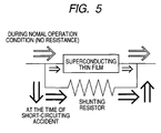
- a shunting resistor must be connected in parallel with the superconducting film as shown in FIG. 5 .
- the superconducting thin film has variation in the local critical current density. Therefore, at the initial time of current-limiting immediately after the accident, the region with the low critical current density first goes into the normal conductive state but the entire region does not go into the normal state. As a result, a large current continues to flow. In the case that the diffusion of heat generated at the region that has become the normal state is slow, the temperature of this region will locally abruptly rise so that the thin film is burned.
- a conventional measure for preventing such a hot spot phenomenon is to deposit a normal conductive metal such as gold or silver on the superconducting thin film, which is used as a shunting layer at the time of transition to the normal state (protective layer for preventing burning) (see Non-Patent Reference 2).
- the area of the superconducting thin film formed on a sapphire substrate necessary for the current-limiting element in a class of 6.6 kV/2 kA can be reduced to about 1/30 of the conventional element.
- This supposedly leads to great cost reduction.
- it is necessary to use a large quantity of a highly thermal conductive ceramic substrate such as aluminum nitride and indium plate. Since these materials are expensive, there has been a limit in cost reduction.
- a pure metal such as gold or silver deposited on the superconducting thin film is used as a shunting layer at the time of transition to the normal state.
- the resistivity of the pure metal is lower by about two orders of magnitude than that of superconducting oxide, so that the resistance of the superconductive path is greatly reduced.
- the quantity of generated heat is increased, so that the sharing electric field of the superconductive thin-film current-limiting element is greatly reduced.
- the required quantity of the expensive superconducting thin film is increased. This is very disadvantageous in cost.
- the pure metal can be deposited very thin (with a film thickness of the order of nanometer) and uniformly on the superconducting thin film, the problem of reduction in the electric resistance can be solved. However, it is not clear whether or not such a deposition technique can be realized. Even if it can be realized, it is not clear where it leads to the solution of the problem of the hot spot.
- An object of the present invention is to solve the problem of the hot spot of a superconducting thin film without greatly reducing the resistance of a superconductive path by depositing an alloy layer having resistivity much higher than a pure metal on the superconducting thin film, and also to provide a superconducting fault-current limiting element capable of attaining a higher sharing electric field by connecting an external noninductively wound shunt resistor made of a pure metal or alloy wire in parallel with the superconducting thin film on which the alloy layer is formed so that the resistance of the superconductive path is increased, and the process for producing the same.
- the present invention adopts the following measures.
- the first measure is a superconducting fault-current limiting element including an insulator substrate; a superconducting thin film formed on the insulator substrate; and an alloy layer formed on the superconducting thin film, said alloy layer having a room-temperature resistivity higher by twice or more than the room-temperature resistivity of a pure metal, in which, when the superconducting thin film goes into a normal conductive state by an overcurrent, the overcurrent flowing through the superconducting thin film is transferred only to the alloy layer.
- the second measure is the superconducting fault-current limiting element according to the first measure, in which the alloy layer includes a binary alloy layer of gold and silver or a multinary alloy layer of gold, silver and other element(s).
- the third measure is a superconducting fault-current limiting element including an insulator substrate; a superconducting thin film formed on the insulator substrate; and an alloy layer formed on the superconducting thin film, said alloy layer having a room-temperature resistivity higher by twice or more than the room-temperature resistivity of a pure metal, in which the superconducting fault-current limiting element further includes a shunt resistor made of a wire of a pure metal or alloy, and the shunt resistor is connected in parallel with the superconducting thin film.
- the fourth measure is a superconducting fault-current limiting element according to the third measure, in which the shunt resistor is made of a noninductively wound wire to thereby give a smaller inductance.
- the fifth measure is a method for fabricating a superconducting fault-current limiting element according to the first measure or third measure, which includes conducting a sputter deposition of the alloy layer on the superconducting thin film formed on the insulator substrate.
- the superconducting fault-current limiting element having a higher sharing electric field can be produced at low cost.
- the superconducting fault-current limiting element having a higher sharing electric field can be realized.
- the alloy having substantially the same composition as that of a target can be easily formed. Good intimate contact with the superconducting thin film can be realized without conducting the subsequent heat treatment, so that a contact resistance between the alloy layer and the superconducting thin film can be reduced.
- FIG. 1 is a view showing the construction of a superconducting thin-film fault-current limiting element according to one embodiment of the invention.
- FIG. 2 is a view showing the construction of a superconducting thin-film fault-current limiting element according to one embodiment of the invention, in which an external noninductively wound shunt resistor made of a pure metal or alloy wire is connected in parallel with the superconducting thin film.
- FIG. 3 is a graph showing the result of a current-limiting test of a superconducting thin-film fault-current limiting element according to one embodiment of the invention.
- FIG. 4 is a graph showing the result of a current-limiting test of a superconducting thin-film fault-current limiting element according to one embodiment of the invention, to which a noninductively wound shunt resistor is connected.
- FIG. 5 is a view showing the construction of a conventional superconducting fault-current limiting element in which a shunting resistor is connected to a superconducting thin film.
- FIGS. 1 to 4 an explanation will be given with regard to one embodiment of the invention.
- FIG. 1 is a view showing the construction of a superconducting thin-film fault-current limiting element.
- reference numeral 1 denotes an insulator substrate of sapphire or the like
- 2 denotes a buffer layer of ceria or the like
- 3 denotes a large-area superconducting oxide thin film
- 4 denotes an alloy layer having a predetermined film thickness deposited on the superconducting oxide thin film 3 .
- the alloy layer 4 may be a binary alloy composed of gold and silver which is stable in the air and does not react with the superconducting oxide thin film 3 .
- the alloy layer 4 has the composition of gold and silver mixed by 7 to 82 wt % therewith, the resistivity thereof at room temperature is twice or more as large as that of pure gold. Therefore, the alloy layer having such a composition is favorable in construction of the superconducting thin-film fault-current limiting element.
- the alloy having the composition in which 23 wt % of silver is mixed to gold, whose resistivity is maximum or about five times as large as pure gold, is supposedly optimum.
- the resistivity of pure gold is reduced to about one third as large as that at room temperature whereas that of the alloy is not nearly reduced. It leads to a difference of about 15 times.
- the alloy layer 4 on the superconducting oxide thin film 3 As a method for depositing the alloy layer 4 on the superconducting oxide thin film 3 , various methods such as vacuum deposition and sputtering can be adopted. However, in the invention, sputtering is adopted.
- the most general vacuum deposition in which an alloy constructed of metals having different melting points is deposited to have a desired composition, has disadvantages that it requires precise control of deposition of constituent metals and requires the subsequent heat treatment owing to poor contact between the deposited alloy film and the superconducting thin film.
- the alloy having substantially the same composition as the target can be easily formed and the good contact with the superconducting oxide film can be obtained without the subsequent heat treatment. Thus, the contact resistance can be reduced so that the resultant structure can be employed as the fault-current limiting element as it is.
- the binary alloy composed of gold and silver is employed as the alloy layer 4 .
- a multinary alloy in which other element is added to gold and silver such as a commercially available 18-carat gold (composed of gold of 75 wt %, silver of 12.5 wt % and copper of 12.5 wt %) is employed, same effect can be obtained.
- FIG. 2 is a view showing the construction of a superconducting thin-film fault-current limiting element in which an external noninductively wound shunt resistor 6 made of a pure metal or alloy wire is connected in parallel with the superconducting oxide thin film 3 in order to realize a higher sharing electric field.
- the above shunt resistor 6 has a resistance much smaller than the composite resistance of the superconducting oxide thin film 3 after the transition to the normal conductive state and the alloy layer 4 .
- reference numeral 5 denotes gold electrodes deposited on both ends of the superconducting oxide thin film 3 .
- Other reference numerals refer to like parts in FIG. 1 .
- the function of the noninductively wound shunt resistor 6 is to further alleviate the problem of hot spot in the superconducting oxide thin film 3 in such a manner that the transfer of an overcurrent at the time of transition to the normal state (initial time of current-limiting) is shared by not only the alloy layer 4 but also by the non-inductive shunting resistor 6 , thereby further increasing the resistance of the superconducting thin-film fault-current limiting element.
- the inductance of the external noninductively wound shunt resistor 6 is as small as possible. For this reason, the shunt resistor was made of a noninductive winding of a cheap alloy wire.
- the sharing electric field of the superconducting thin-film fault-current limiting element must be determined so that the temperature of the current-limiting element does not rise to room temperature or higher during the current-limiting operation.
- the external noninductively wound shunt resistor 6 having a small resistance considerable heat is generated at this area.
- the temperature rise can be suppressed by using the noninductively wound shunt resistor having a sufficiently large heat capacity. Therefore, the heat generated in the noninductively wound shunt resistor 6 will not cause to reduce the sharing electric field of the body of the superconducting thin-film current-limiting element.
- a YBCO thin film (DC critical current of 45 A) having a thickness of 300 nm and a critical current density of 3 MA/cm 2 is formed on a sapphire substrate having a size of 5 mm ⁇ 60 mm ⁇ 1 mm.
- gold is deposited to provide electrodes.
- an Au—Ag alloy layer having a film thickness of about 100 nm is deposited by sputtering.
- the resistance of the superconducting thin-film fault-current limiting element at room temperature was reduced to about 1/7 as compared with the case where only the YBCO layer is used (about 60 ⁇ ).
- FIG. 3 is a graph showing the result of the current-limiting test using the above superconducting fault-current limiting element.
- FIG. 4 is a graph showing the result of a current-limiting test using the above superconducting thin-film fault-current limiting element.
- the superconducting fault-current limiting element of the YBCO thin film which does not have the shunting protective layer such as the alloy layer was prepared.
- the same current-limiting test was carried out. In this test, when the AC passing current is instantaneously increased to about 30 A peak to about 60 A peak , a part of the thin film was burned during the current passing during one cycle, which resulted in an insulating state. Thus, it was confirmed that the thin film having such a high critical current density cannot realize the current-limiting operation without the measure for obviating the hot spot.
Landscapes
- Emergency Protection Circuit Devices (AREA)
- Containers, Films, And Cooling For Superconductive Devices (AREA)
- Superconductors And Manufacturing Methods Therefor (AREA)
Applications Claiming Priority (4)
| Application Number | Priority Date | Filing Date | Title |
|---|---|---|---|
| JP2004186966 | 2004-06-24 | ||
| JPP.2004-186966 | 2004-06-24 | ||
| JP2004-186966 | 2004-06-24 | ||
| PCT/JP2005/011117 WO2006001226A1 (ja) | 2004-06-24 | 2005-06-17 | 超電導限流素子及びその作製方法 |
Publications (2)
| Publication Number | Publication Date |
|---|---|
| US20080026946A1 US20080026946A1 (en) | 2008-01-31 |
| US8088713B2 true US8088713B2 (en) | 2012-01-03 |
Family
ID=35781714
Family Applications (1)
| Application Number | Title | Priority Date | Filing Date |
|---|---|---|---|
| US11/630,478 Expired - Fee Related US8088713B2 (en) | 2004-06-24 | 2005-06-17 | Superconducting fault-current limiting element and the process for producing the same |
Country Status (5)
| Country | Link |
|---|---|
| US (1) | US8088713B2 (ja) |
| JP (1) | JP4644779B2 (ja) |
| CN (1) | CN1973381A (ja) |
| DE (1) | DE112005001495B4 (ja) |
| WO (1) | WO2006001226A1 (ja) |
Cited By (1)
| Publication number | Priority date | Publication date | Assignee | Title |
|---|---|---|---|---|
| KR20170122530A (ko) * | 2016-04-27 | 2017-11-06 | 인하공업전문대학산학협력단 | 무유도 저항의 제조 방법 및 제조 장치 |
Families Citing this family (9)
| Publication number | Priority date | Publication date | Assignee | Title |
|---|---|---|---|---|
| JP5152830B2 (ja) * | 2007-05-14 | 2013-02-27 | 独立行政法人産業技術総合研究所 | 超電導限流素子 |
| JP2009049257A (ja) * | 2007-08-22 | 2009-03-05 | National Institute Of Advanced Industrial & Technology | 超電導限流素子 |
| EP2117056B1 (en) * | 2008-03-05 | 2010-11-03 | Bruker HTS GmbH | Superconducting device for current conditioning |
| JP5472682B2 (ja) * | 2009-05-01 | 2014-04-16 | 独立行政法人産業技術総合研究所 | 超電導限流素子 |
| SG195087A1 (en) * | 2011-05-24 | 2013-12-30 | Furukawa Electric Co Ltd | Superconducting element for superconducting current limiter, method for manufacturing superconducting element for superconducting current limiter, and superconducting current limiter |
| US9105794B2 (en) | 2011-05-31 | 2015-08-11 | Furukawa Electric Co., Ltd. | Oxide superconductor thin film, superconducting fault current limiter, and method for manufacturing oxide superconductor thin film |
| CN105976939A (zh) * | 2016-05-05 | 2016-09-28 | 成都君禾天成科技有限公司 | 基于化学溶液法制备铋系超导薄膜的方法 |
| US11441954B2 (en) * | 2019-01-30 | 2022-09-13 | King Fahd University Of Petroleum And Minerals | Method, system and apparatus for measuring rest time of superconducting nanowire |
| CN111244921A (zh) * | 2020-03-09 | 2020-06-05 | 广东电网有限责任公司电力科学研究院 | 一种混合式直流超导限流器及短路电流限制方法 |
Citations (14)
| Publication number | Priority date | Publication date | Assignee | Title |
|---|---|---|---|---|
| JPH05251761A (ja) | 1992-03-04 | 1993-09-28 | Mitsubishi Electric Corp | 酸化物超電導膜を用いた限流導体 |
| CA2083566A1 (en) * | 1992-11-23 | 1994-05-24 | Paul Lambert | Alloy for htsc composite conductors |
| US5361055A (en) * | 1993-12-17 | 1994-11-01 | General Dynamics Corporation | Persistent protective switch for superconductive magnets |
| US5430012A (en) * | 1991-12-02 | 1995-07-04 | Sumitomo Electric Industries, Ltd. | Superconducting multilayer interconnection formed of a-axis and c-axis oriented oxide superconductor materials |
| JPH0883932A (ja) | 1994-09-09 | 1996-03-26 | Sumitomo Electric Ind Ltd | 限流素子 |
| EP0828333A2 (de) | 1996-08-26 | 1998-03-11 | Abb Research Ltd. | Verfahren zur Herstellung eines Strombegrenzers mit einem Hochtemperatur-Supraleiter und Strombegrenzer |
| JP2954124B2 (ja) | 1998-01-07 | 1999-09-27 | 株式会社東芝 | 超電導限流素子 |
| US5969928A (en) * | 1997-12-03 | 1999-10-19 | Gould Electronics Inc. | Shunt for circuit protection device |
| US6051846A (en) * | 1993-04-01 | 2000-04-18 | The United States Of America As Represented By The Secretary Of The Navy | Monolithic integrated high-Tc superconductor-semiconductor structure |
| DE19963181A1 (de) | 1999-12-27 | 2001-07-05 | Siemens Ag | Resistive Strombegrenzereinrichtung für Gleich- oder Wechselstrom mit wenigstens einer Leiterbahn mit Hoch-T¶c¶-Supraleitermaterial |
| JP2002198577A (ja) | 2000-12-27 | 2002-07-12 | Mitsubishi Electric Corp | 超電導薄膜限流器 |
| US6522236B1 (en) * | 1997-12-19 | 2003-02-18 | Siemens Aktiengesellschaft | Superconductor structure with high Tc superconductor material, process for producing the structure, and current limiter device having such a structure |
| US6524684B1 (en) * | 1998-12-08 | 2003-02-25 | Siemens Aktiengesellschaft | Resistive current-limiting device with at least one printed conductor covered by an insulating layer by using high Tc superconductive material |
| JP2003153437A (ja) | 2001-11-13 | 2003-05-23 | Nisshin Denki Seisakusho:Kk | 通信線の保安器 |
Family Cites Families (3)
| Publication number | Priority date | Publication date | Assignee | Title |
|---|---|---|---|---|
| JP3977884B2 (ja) * | 1996-10-25 | 2007-09-19 | 新日本製鐵株式会社 | 酸化物超電導体を用いた限流素子、限流器およびその製造方法 |
| JP3806479B2 (ja) * | 1997-01-29 | 2006-08-09 | 株式会社日立製作所 | 変流器 |
| JP3872738B2 (ja) * | 2002-09-04 | 2007-01-24 | 新日本製鐵株式会社 | 高耐電圧超電導限流器 |
-
2005
- 2005-06-17 CN CNA2005800209317A patent/CN1973381A/zh active Pending
- 2005-06-17 WO PCT/JP2005/011117 patent/WO2006001226A1/ja active Application Filing
- 2005-06-17 DE DE112005001495T patent/DE112005001495B4/de not_active Expired - Fee Related
- 2005-06-17 US US11/630,478 patent/US8088713B2/en not_active Expired - Fee Related
- 2005-06-17 JP JP2006528493A patent/JP4644779B2/ja not_active Expired - Fee Related
Patent Citations (14)
| Publication number | Priority date | Publication date | Assignee | Title |
|---|---|---|---|---|
| US5430012A (en) * | 1991-12-02 | 1995-07-04 | Sumitomo Electric Industries, Ltd. | Superconducting multilayer interconnection formed of a-axis and c-axis oriented oxide superconductor materials |
| JPH05251761A (ja) | 1992-03-04 | 1993-09-28 | Mitsubishi Electric Corp | 酸化物超電導膜を用いた限流導体 |
| CA2083566A1 (en) * | 1992-11-23 | 1994-05-24 | Paul Lambert | Alloy for htsc composite conductors |
| US6051846A (en) * | 1993-04-01 | 2000-04-18 | The United States Of America As Represented By The Secretary Of The Navy | Monolithic integrated high-Tc superconductor-semiconductor structure |
| US5361055A (en) * | 1993-12-17 | 1994-11-01 | General Dynamics Corporation | Persistent protective switch for superconductive magnets |
| JPH0883932A (ja) | 1994-09-09 | 1996-03-26 | Sumitomo Electric Ind Ltd | 限流素子 |
| EP0828333A2 (de) | 1996-08-26 | 1998-03-11 | Abb Research Ltd. | Verfahren zur Herstellung eines Strombegrenzers mit einem Hochtemperatur-Supraleiter und Strombegrenzer |
| US5969928A (en) * | 1997-12-03 | 1999-10-19 | Gould Electronics Inc. | Shunt for circuit protection device |
| US6522236B1 (en) * | 1997-12-19 | 2003-02-18 | Siemens Aktiengesellschaft | Superconductor structure with high Tc superconductor material, process for producing the structure, and current limiter device having such a structure |
| JP2954124B2 (ja) | 1998-01-07 | 1999-09-27 | 株式会社東芝 | 超電導限流素子 |
| US6524684B1 (en) * | 1998-12-08 | 2003-02-25 | Siemens Aktiengesellschaft | Resistive current-limiting device with at least one printed conductor covered by an insulating layer by using high Tc superconductive material |
| DE19963181A1 (de) | 1999-12-27 | 2001-07-05 | Siemens Ag | Resistive Strombegrenzereinrichtung für Gleich- oder Wechselstrom mit wenigstens einer Leiterbahn mit Hoch-T¶c¶-Supraleitermaterial |
| JP2002198577A (ja) | 2000-12-27 | 2002-07-12 | Mitsubishi Electric Corp | 超電導薄膜限流器 |
| JP2003153437A (ja) | 2001-11-13 | 2003-05-23 | Nisshin Denki Seisakusho:Kk | 通信線の保安器 |
Non-Patent Citations (7)
| Title |
|---|
| A. Heinrich et al., "Fault Current Limiting Properties of YBCO-Films on Sapphire Substrates," IEEE Transactions on Applied Superconductivity, vol. 9, No. 2, Jun. 1999, pp. 660-663. |
| B. Gromoll et al., "Resistive Fault Current Limiters with YBCO Films-100 kVA Functional Model," IEEE Transactions on Applied Superconductivity, vol. 9, No. 2, Jun. 1999, pp. 656-659. |
| H. Kubota et al., "A New Model of Fault Current Limiter using YBCO Thin Film," IEEE Transactions on Applied Superconductivity, vol. 9, No. 2, Jun. 1999, pp. 1365-1368. |
| Hirofumi Yamasaki et al., "High-Power-Density Fault-Current Limiting Devices Using Superconducting YBa2Cu3O7 Films and High-Resistivity Alloy Shunt Layers" Applied Physics Letters, vol. 85, No. 19, Nov. 8, 2004, pp. 4427-4429. |
| Hiroshi Kubota et al., "Design of a Fault Current Limiter using YBCO Thin Film," Abstract of the 64th Meeting on Cryogenics and Superconductivity, 2001, p. 166. |
| Machine translation of Shimohata (JP2002-198577). * |
| Machine translation Okuda (JP08-083932). * |
Cited By (2)
| Publication number | Priority date | Publication date | Assignee | Title |
|---|---|---|---|---|
| KR20170122530A (ko) * | 2016-04-27 | 2017-11-06 | 인하공업전문대학산학협력단 | 무유도 저항의 제조 방법 및 제조 장치 |
| KR101880677B1 (ko) * | 2016-04-27 | 2018-07-20 | 인하공업전문대학산학협력단 | 무유도 저항의 제조 방법 및 제조 장치 |
Also Published As
| Publication number | Publication date |
|---|---|
| CN1973381A (zh) | 2007-05-30 |
| DE112005001495B4 (de) | 2011-06-16 |
| JP4644779B2 (ja) | 2011-03-02 |
| DE112005001495T5 (de) | 2007-05-16 |
| JPWO2006001226A1 (ja) | 2008-04-17 |
| WO2006001226A1 (ja) | 2006-01-05 |
| US20080026946A1 (en) | 2008-01-31 |
Similar Documents
| Publication | Publication Date | Title |
|---|---|---|
| US8088713B2 (en) | Superconducting fault-current limiting element and the process for producing the same | |
| US5828291A (en) | Multiple compound conductor current-limiting device | |
| JP2007189228A5 (ja) | ||
| Escamez et al. | Numerical investigations of ReBCO conductors with high limitation electric field for HVDC SFCL | |
| JP4112884B2 (ja) | 超電導部材 | |
| Cantoni et al. | Conductive buffer layers and overlayers for the thermal stability of coated conductors | |
| JP3977884B2 (ja) | 酸化物超電導体を用いた限流素子、限流器およびその製造方法 | |
| JP2009049257A (ja) | 超電導限流素子 | |
| JP2001217470A (ja) | 高温超電導体素子その製造方法 | |
| JP5152830B2 (ja) | 超電導限流素子 | |
| JP5675232B2 (ja) | 超電導電流リード | |
| CN111834043B (zh) | 一种接触电阻可控的高温超导带材结构及制备方法 | |
| JP4131769B2 (ja) | 超電導限流ヒューズおよびこれを用いた過電流制御システム | |
| JPH05251761A (ja) | 酸化物超電導膜を用いた限流導体 | |
| US5179071A (en) | High Tc superconductor contact unit having low interface resistivity | |
| JP4171253B2 (ja) | 低抵抗複合導体およびその製造方法 | |
| JPH03156809A (ja) | 酸化物超電導導体の使用方法 | |
| WO2016020715A1 (en) | Current limiter arrangement and method for manufacturing a current limiter arrangement | |
| JP5472682B2 (ja) | 超電導限流素子 | |
| US20110045988A1 (en) | High-temperature superconducting ribbon conductor composite provided with a cooling layer | |
| CA2177169C (en) | Current-limiting device | |
| Arai et al. | Temperature characteristics of superconducting thin-film fault current limiting elements using high-resistivity alloy shunt layers | |
| JP2002016299A (ja) | 超電導限流素子 | |
| Furuse et al. | Current limiting properties of MOD-YBCO thin films stabilized with high-resistivity alloy shunt layer | |
| JPH05251758A (ja) | 酸化物超電導限流導体の製造方法 |
Legal Events
| Date | Code | Title | Description |
|---|---|---|---|
| AS | Assignment |
Owner name: NATIONAL INSTITUTE OF ADVANCED INDUSTRIAL SCIENCE Free format text: ASSIGNMENT OF ASSIGNORS INTEREST;ASSIGNORS:YAMASAKI, HIROFUMI;FURUSE, MITSUHO;REEL/FRAME:018739/0051 Effective date: 20061214 |
|
| STCF | Information on status: patent grant |
Free format text: PATENTED CASE |
|
| FEPP | Fee payment procedure |
Free format text: PAYOR NUMBER ASSIGNED (ORIGINAL EVENT CODE: ASPN); ENTITY STATUS OF PATENT OWNER: LARGE ENTITY |
|
| FEPP | Fee payment procedure |
Free format text: PAYOR NUMBER ASSIGNED (ORIGINAL EVENT CODE: ASPN); ENTITY STATUS OF PATENT OWNER: LARGE ENTITY Free format text: PAYER NUMBER DE-ASSIGNED (ORIGINAL EVENT CODE: RMPN); ENTITY STATUS OF PATENT OWNER: LARGE ENTITY |
|
| FPAY | Fee payment |
Year of fee payment: 4 |
|
| FEPP | Fee payment procedure |
Free format text: MAINTENANCE FEE REMINDER MAILED (ORIGINAL EVENT CODE: REM.); ENTITY STATUS OF PATENT OWNER: LARGE ENTITY |
|
| LAPS | Lapse for failure to pay maintenance fees |
Free format text: PATENT EXPIRED FOR FAILURE TO PAY MAINTENANCE FEES (ORIGINAL EVENT CODE: EXP.); ENTITY STATUS OF PATENT OWNER: LARGE ENTITY |
|
| STCH | Information on status: patent discontinuation |
Free format text: PATENT EXPIRED DUE TO NONPAYMENT OF MAINTENANCE FEES UNDER 37 CFR 1.362 |
|
| FP | Lapsed due to failure to pay maintenance fee |
Effective date: 20200103 |