US8072133B2 - Light emitter substrate and image displaying apparatus using the same - Google Patents
Light emitter substrate and image displaying apparatus using the same Download PDFInfo
- Publication number
- US8072133B2 US8072133B2 US12/476,532 US47653209A US8072133B2 US 8072133 B2 US8072133 B2 US 8072133B2 US 47653209 A US47653209 A US 47653209A US 8072133 B2 US8072133 B2 US 8072133B2
- Authority
- US
- United States
- Prior art keywords
- row
- light
- electrodes
- substrate
- light emitter
- Prior art date
- Legal status (The legal status is an assumption and is not a legal conclusion. Google has not performed a legal analysis and makes no representation as to the accuracy of the status listed.)
- Expired - Fee Related, expires
Links
Images


Classifications
-
- H—ELECTRICITY
- H01—ELECTRIC ELEMENTS
- H01J—ELECTRIC DISCHARGE TUBES OR DISCHARGE LAMPS
- H01J1/00—Details of electrodes, of magnetic control means, of screens, or of the mounting or spacing thereof, common to two or more basic types of discharge tubes or lamps
- H01J1/53—Electrodes intimately associated with a screen on or from which an image or pattern is formed, picked-up, converted, or stored
-
- H—ELECTRICITY
- H01—ELECTRIC ELEMENTS
- H01J—ELECTRIC DISCHARGE TUBES OR DISCHARGE LAMPS
- H01J29/00—Details of cathode-ray tubes or of electron-beam tubes of the types covered by group H01J31/00
- H01J29/02—Electrodes; Screens; Mounting, supporting, spacing or insulating thereof
- H01J29/08—Electrodes intimately associated with a screen on or from which an image or pattern is formed, picked-up, converted or stored, e.g. backing-plates for storage tubes or collecting secondary electrons
- H01J29/085—Anode plates, e.g. for screens of flat panel displays
-
- H—ELECTRICITY
- H01—ELECTRIC ELEMENTS
- H01J—ELECTRIC DISCHARGE TUBES OR DISCHARGE LAMPS
- H01J31/00—Cathode ray tubes; Electron beam tubes
- H01J31/08—Cathode ray tubes; Electron beam tubes having a screen on or from which an image or pattern is formed, picked up, converted, or stored
- H01J31/10—Image or pattern display tubes, i.e. having electrical input and optical output; Flying-spot tubes for scanning purposes
- H01J31/12—Image or pattern display tubes, i.e. having electrical input and optical output; Flying-spot tubes for scanning purposes with luminescent screen
- H01J31/123—Flat display tubes
- H01J31/125—Flat display tubes provided with control means permitting the electron beam to reach selected parts of the screen, e.g. digital selection
- H01J31/127—Flat display tubes provided with control means permitting the electron beam to reach selected parts of the screen, e.g. digital selection using large area or array sources, i.e. essentially a source for each pixel group
-
- H—ELECTRICITY
- H01—ELECTRIC ELEMENTS
- H01J—ELECTRIC DISCHARGE TUBES OR DISCHARGE LAMPS
- H01J2329/00—Electron emission display panels, e.g. field emission display panels
- H01J2329/02—Electrodes other than control electrodes
- H01J2329/08—Anode electrodes
-
- H—ELECTRICITY
- H01—ELECTRIC ELEMENTS
- H01J—ELECTRIC DISCHARGE TUBES OR DISCHARGE LAMPS
- H01J2329/00—Electron emission display panels, e.g. field emission display panels
- H01J2329/18—Luminescent screens
- H01J2329/28—Luminescent screens with protective, conductive or reflective layers
Definitions
- the present invention relates to a light emitter substrate and an image displaying apparatus which uses the light emitter substrate.
- an image displaying apparatus which comprises an electron source substrate having plural electron-emitting devices arranged in matrix and a light emitter substrate having plural light-emitting members arranged in matrix and opposed to the plural electron-emitting devices has been known.
- the light emitter substrate and the electron source substrate are typically opposed to each other at a gap of about several millimeters, and high voltage of, e.g., approximately 10 kV is applied between these substrates.
- high voltage e.g., approximately 10 kV
- Japanese Patent Application Laid-Open No. 2006-173094 corresponding to U.S. Patent Publication No. 2006/0103294 and Japanese Patent Application Laid-Open No. 2006-185632 corresponding to European Patent Publication No. 1830379A1 respectively disclose techniques for controlling a discharging current by two-dimensionally dividing a metal back and establishing a connection between the divided metal backs by a resistor.
- Japanese Patent Application Laid-Open Nos. 2006-173094 and 2006-185632 it is designed to define resistance in the row direction without arranging any resistor between light-emitting members adjacent in the row direction. More specifically, Japanese Patent Application Laid-Open No. 2006-173094 discloses the structure that the metal back divided in matrix and the resistors patterned in matrix are combined, and any resistor is not arranged between the metal backs adjacent in the row direction. Further, Japanese Patent Application Laid-Open No. 2006-185632 discloses the structure that the metal backs divided in matrix and striped resistors expanding in the row direction between the metal backs adjacent in a column direction are connected on the column side of the light-emitting members.
- the present invention aims to improve, in a light emitter substrate which has a resistor for connecting electrodes adjacent in a row direction, withstand discharge performance of the resistor. Moreover, the present invention aims to provide an image displaying apparatus which uses the light emitter substrate like this.
- a light emitter substrate comprises a substrate, plural light-emitting members which are positioned in matrix on the substrate, plural electrodes each of which covers at least one of the light-emitting members and which are positioned in matrix, and a row-direction resistor which is positioned between the electrodes adjacent to each other in a row direction and connects these electrodes to each other.
- the light emitter substrate is characterized in that a row-direction separated distance between the electrodes adjacent to each other in the row direction at a connecting portion between the electrodes and the row-direction resistor is larger than a row-direction separated distance between the electrodes adjacent to each other in the row direction at a portion covering the light-emitting members.
- an image displaying apparatus comprises: an electron source substrate having plural electron-emitting devices; and the above-described light emitter substrate, wherein the light-emitting members of the light emitter substrate emit light in response to electrons emitted from the electron-emitting devices.
- the present invention in the light emitter substrate which has the resistor for connecting the electrodes adjacent in the row direction, it is possible to improve the withstand discharge performance of the resistor. Moreover, according to the present invention, it is possible to provide the image displaying apparatus which uses the light emitter substrate like this.
- FIG. 1 is a partial fractured perspective view illustrating the basic structure of an image displaying apparatus according to an embodiment of the present invention.
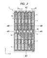
- FIG. 2 is an inner face view of a light emitter substrate illustrated in FIG. 1 .
- FIG. 3 is a plane view illustrating an arrangement pattern of a black member and light-emitting members in the light emitter substrate illustrated in FIG. 1 .
- FIGS. 4A , 4 B and 4 C are respectively a 4 A- 4 A cross-sectional view, a 4 B- 4 B cross-sectional view and a 4 C- 4 C cross-sectional view in FIG. 2 .
- FIG. 5 is an inner face view of a light emitter substrate according to another embodiment of the present invention.
- FIG. 6 is an inner face view of a light emitter substrate according to still another embodiment of the present invention.
- a light emitter substrate of the present invention can be applied to an electron beam displaying apparatus such as a CRT (Cathode Ray Tube) or an FED (Field Emission Display).
- an electron beam displaying apparatus such as a CRT (Cathode Ray Tube) or an FED (Field Emission Display).
- the FED is a preferable form to which the present invention is applied.
- FIG. 1 is a partial fractured perspective view illustrating the basic structure of an image displaying apparatus according to an embodiment of the present invention.
- An image displaying apparatus 15 has an electron source substrate 8 , which has the two-dimensionally arranged plural surface conduction electron-emitting devices 12 , and a light emitter substrate 1 , which is arranged opposite to the electron source substrate 8 .
- the light emitter substrate 1 and the electron source substrate 8 form a vacuum envelope 14 together with an outer frame 13 .
- a spacer (not illustrated), which mutually supports the electron source substrate 8 and the light emitter substrate 1 may be provided inside the vacuum envelope 14 depending on a size of the image displaying apparatus.
- the image displaying apparatus 15 is constituted by adding a power supply, a driver circuit and the like, which are not illustrated, to the vacuum envelope 14 .
- the electron source substrate 8 has a glass substrate 9 , row wirings (scanning wirings) 10 and column wirings (signal wirings) 11 formed on the glass substrate 9 and the surface conduction electron-emitting devices 12 .
- the number of the row wirings 10 is N and the number of the column wirings 11 is M, and the N ⁇ M surface conduction electron-emitting devices 12 are formed.
- the N and M which are positive integers, can be arbitrarily set in accordance with the intended number of display pixels. For example, in case of an FHD (Full High Definition) panel, the N is equal to 1080 and the M is equal to 1920 ⁇ 3, that is, 5760.
- a metal back 5 is electrically connected with a terminal Hv of the vacuum envelope 14 , and a high voltage of about 1 kV to 15 kV is applied by a high voltage power supply which is not illustrated.
- the scanning wirings 10 and the signal wirings 11 are respectively connected with terminals Dyn (n denotes positive integers 1 to N) and terminals Dxm (m denotes positive integers 1 to M) of the vacuum envelope 14 , and scanning signals and image signals are respectively given by a driver circuit which is not illustrated.
- the surface conduction electron-emitting devices 12 emit electrons according to the signals, and the electrons attracted by the metal back potential pass through the metal back 5 to make emit light from the phosphor of a light-emitting member 4 .
- the luminance can be adjusted by the voltage or the signals.
- FIG. 2 is an inner face view of the above-described light emitter substrate.
- FIG. 3 is a plane view illustrating an arrangement pattern of a black member and light-emitting members.
- FIGS. 4A , 4 B and 4 C are respectively a 4 A- 4 A cross-sectional view, a 4 B- 4 B cross-sectional view and a 4 C- 4 C cross-sectional view in FIG. 2 .
- an illustration of the metal back is omitted in a left lower part in the drawing (an illustration, in which the metal back was stripped off, is indicated).
- FIGS. 2 , 3 , 4 A, 4 B and 4 C the constitution of the light emitter substrate will be described with reference to FIGS. 2 , 3 , 4 A, 4 B and 4 C.
- the light emitter substrate 1 has a substrate 2 . It is preferable to use a glass substrate for the substrate 2 especially in a point that the vacuum performance is maintained and the intensity is ensured.
- a black member 3 is provided on the substrate 2 .
- the black member 3 which has apertures, is formed in a lattice-like shape.
- the light-emitting members 4 consisted of the phosphors are formed on the apertures.
- the light-emitting members 4 are color-coded by R (Red), G (Green) and B (Blue) in case of a color display.
- the color-coding pattern can be arbitrarily determined in accordance with the display characteristics and that pattern is not limited to the present embodiment. In FIG. 3 , a pattern of color coding the phosphors in a striped form to the lattice-like black member is illustrated.
- plural metal backs (electrodes) 5 which cover the two light-emitting members 4 which are two dimensionally arranged and adjacent to each other in the column direction (Y direction), are further provided on the substrate 2 .
- a row-direction resistor 6 (resistance Rx) for electrically connecting the metal backs 5 adjacent to each other in the row direction (X direction)
- column-direction resistors 7 (resistance Ry) for electrically connecting the metal backs 5 adjacent to each other in the column direction (Y direction) are provided on the substrate 2 .
- Rx row-direction resistor 6
- Ry column-direction resistors 7
- the row-direction resistors 6 may be discretely provided only between the metal backs 5 adjacent to each other in the row direction (X direction). In other words, it is allowed to be constituted that the row-direction resistor 6 is provided at least between the metal backs 5 adjacent to each other in the row direction (X direction) to serve to electrically connect the metal backs 5 adjacent to each other in the row direction (X direction).
- the column-direction resistors 7 are discretely provided only between the metal backs 5 adjacent to each other in the column direction (Y direction) as illustrated in FIG. 4C .
- the light emitter substrate 1 of the present embodiment plural light-emitting members 4 arranged in matrix on the substrate 2 are formed, and spaces between the light-emitting members 4 are partitioned by the black member 3 .
- the row-direction resistor 6 continuously extended in the row direction (X direction) is formed on the black member 3 .
- the column-direction resistors 7 are discretely provided in the column direction (Y direction) on the black member 3 .
- a large number of metal backs 5 each of which covers the two light-emitting members 4 , are formed on these members. Although the adjacent metal backs 5 are not directly connected each other, the metal backs are electrically connected in the row direction (X direction) and the column direction (Y direction) respectively by the row-direction resistor 6 and the column-direction resistors 7 .
- the row-direction resistor 6 is arranged on positions where the width of the metal backs 5 became a narrow state (positions indicated by a 4 A- 4 A line illustrated in FIG. 2 ) to be connected with the metal backs 5 .
- the width Mx′ in the row direction at a portion of covering the row-direction resistor 6 of the metal backs 5 is narrower than the width Mx in the row direction at a position of covering the light-emitting members 4 . That is, a separated distance Gx′ between the metal backs 5 adjacent to each other in the row direction at a portion of connecting with the row-direction resistor 6 is longer than a separated distance Gx between the metal backs 5 in the row direction between the light-emitting members 4 .
- the field intensity given to the row-direction resistor 6 due to the potential difference between the adjacent metal backs 5 generated when the discharge occurred can be weakened, and the breakdown of the row-direction resistor 6 can be prevented.
- a length of the row-direction resistor 6 can be easily secured by keeping the separated distance Gx′ between the metal backs to become long at a connecting position of the row-direction resistor 6 .
- the row-direction resistor 6 can easily withstand the potential difference between the adjacent metal backs, and the anode (metal back) voltage can be more increased. Therefore, a light emitter substrate capable of displaying a high-luminance image can be obtained.
- the metal back 5 may cover the light-emitting members 4 equal to or more than three (P pieces) adjacent to each other in the Y direction.
- (P ⁇ 1) lines of the row-direction resistors can be arranged at a maximum level corresponding to the metal backs 5 , and this constitution is effective as a resistance adjusting means.
- the resistance Rx can be decreased even if the volume resistance is increased, it becomes possible to increase the discharge voltage of the row-direction resistor 6 under the condition of increasing the volume resistance.
- the metal back 5 may cover the plural light-emitting members 4 in the row direction (X direction).
- the width Mx′ at a position of connecting with the row-direction resistor can be enormously narrowed as compared with the width Mx in the row direction (X direction) at a position of covering the light-emitting members 4 .
- the separated distance Gx′ between the metal backs adjacent to each other in the row direction at a portion of connecting with the resistor 6 can be made longer than the separated distance Gx at a position of covering the light-emitting members 4 , and it is preferable to become advantageous in an aspect of the discharge voltage.
- the metal backs 5 can be patterned by a masking process or an etching process by using a generally known deposition method. In particular, it is preferable to perform a mask vapor deposition method because of its simplicity.
- the resistors 6 and 7 can be formed by a generally known manufacturing method such as a pattern printing method, a dispenser application method or a photolithography method.
- the pattern printing method is preferable from a viewpoint of accuracy and productivity.
- FIG. 2 is an inner face view, where a metal back of the light emitter substrate is partially cut off.
- the light emitter substrate of this example was manufactured as described below.
- a lattice-like shape which has apertures only on desired regions in a light emitting region, is screen printed on a surface of a cleaned glass substrate by using a black paste (NP-7803D available by Noritake Co., Ltd.), and the glass substrate is baked at the temperature 550° C. after drying it at the temperature 120° C. to form a black member 3 of which thickness is 5 ⁇ m.
- Pitches of aperture portions were set to become 450 ⁇ m in the Y direction and 150 ⁇ m in the X direction, which are same as those in device pitches on a rear plate, and the size of an aperture portion is set to become 220 ⁇ m in the Y direction and 90 ⁇ m in the X direction.
- This paste printed on the black member was baked at the temperature 530° C. after drying it for ten minutes at the temperature 120° C.
- the row-direction resistors 6 were formed for all the rows every two rows on a row direction pattern of the black member 3 .
- the column-direction resistors 7 were formed between apertures of the black member 3 of interleaving the row direction pattern every column on the row direction pattern where the row-direction resistors 6 are not arranged.
- the volume resistance of the high-resistance paste after the baking was set to become 2 ⁇ m, and the width of the row-direction resistor 6 was set to become 50 ⁇ m and the width of the column-direction resistor 7 was set to become 80 ⁇ m.
- a paste in which a phosphor P22 used in a field of a CRT was dispersed, was printed on apertures of the black member 3 by the screen printing method as the light-emitting members 4 .
- the phosphors of three colors of R, G and B are color-coded with a striped shape such that a display becomes to act as a color display.
- the film thickness of each phosphor was set to become 15 ⁇ m.
- the phosphors of three colors of R, G and B were dried at the temperature 120° C. after the printing. A drying process may be executed for each of colors or the three colors.
- an alkaline solution of silicic acid that is, a water solution of including liquid glass acting as the bonding agent later was spray applied.
- an acrylic emulsion is applied by a spray coating method and dried to infill gaps in the phosphor powder with the acrylic resin, and an aluminum film serving as the metal back 5 was vapor deposited.
- a metal mask which has aperture portions on at least the portions corresponding to apertures of the black member 3 is used, and the metal backs 5 were formed on the light-emitting members 4 .
- the thickness of aluminum was set to become 100 nm. Thereafter, the above-described resin was made to be decomposed and eliminated by heating the resin at the temperature 450° C.
- the metal backs 5 which are formed from wide width portions, where the X-direction width (Mx) is 100 ⁇ m and the Y-direction width (My) is 330 ⁇ m, and narrow width portions, where the row direction width (Mx′) is 50 ⁇ m and the column direction width (My′) is 120 ⁇ m, were formed by an aluminum film. Note that the row-direction resistors 6 are set to be fitted into the range of the above-described narrow width portions in portions of connecting with the metal backs.
- An SED is manufactured by using a light emitter substrate 1 manufactured in this manner, and a discharge between the light emitter substrate 1 and the electron source substrate 8 was induced by ingenerating the device destruction by applying the voltage of 10 kV between the light emitter substrate 1 and the electron source substrate 8 and applying the excessive voltage to a specific device.
- a discharge current was also controlled as expected. Additionally, although the damage of devices was confirmed by lighting up a whole surface with white after the discharge experiment, the damage could not be confirmed in peripheral devices other than the device purposely destructed.
- Example 2 This example is different from Example 1 in a point that the metal back 5 is formed to cover the three light-emitting members 4 adjacent to each other in the column direction (Y direction) as illustrated in FIG. 5 .
- the row-direction resistors 6 are arranged corresponding to narrow width portions of the metal backs.
- the column-direction resistors 7 are arranged on the rows where the row-direction resistors 6 are not arranged, that is, arranged every three rows.
- a light emitter substrate 16 manufactured in this manner although the resistance design is same as that in Example 1, the volume resistance of a resistant paste can be doubled, and the discharge voltage of the row-direction resistors 6 and the column-direction resistors 7 can be increased.
- An SED is manufactured by using this light emitter substrate 16 , and when a discharge inducing experiment similar to that in Example 1 was conducted by applying the voltage of 10 kV between the light emitter substrate 16 and the electron source substrate 8 , a discharge current equivalent to that in Example 1 was observed.
- the similar discharge experiment was conducted under the condition of increasing the voltage to 12 kV, the light emission due to the discharge was observed only in the vicinity of the destructed device, and the light emission suggesting the breakdown of the row-direction resistors 6 or the column-direction resistors 7 was not confirmed.
- a discharge current was also controlled as expected.
- the damage of devices was confirmed by lighting up a whole surface with white after a discharge experiment, the damage could not be confirmed in peripheral devices other than the device purposely destructed.
- Example 2 This example is different from Example 1 in a point that the metal back 5 is formed to cover the six light-emitting members 4 in total consisted by two members adjacent to each other in the column direction and three members adjacent to each other in the row direction as illustrated in FIG. 6 .
- the column-direction resistors 7 are arranged on the rows where the row-direction resistors 6 are not arranged, that is, one line is arranged every two columns. That is, one line is arranged between the metal backs adjacent to each other in the column direction (Y direction).
- the row direction width (Mx) and the column direction width (My) at portions of covering the light-emitting members 4 of the metal backs 5 were respectively set to become 350 ⁇ m and 330 ⁇ m, and the row direction width (Mx′) and the column direction width (My′) on narrow width portions were respectively set to become 150 ⁇ m and 120 ⁇ m.
- the separated distance (Gx) between the metal backs adjacent to each other in the row direction at portions of covering the light-emitting members was 50 ⁇ m similar to that in Example 1.
- An SED is manufactured by using this light emitter substrate 17 , and when a discharge inducing experiment similar to that in Example 1 was conducted by applying the voltage of 10 kV between the light emitter substrate 17 and the electron source substrate 8 , a discharge current equivalent to that in Example 1 was observed.
- the similar discharge experiment was conducted under the condition of increasing the voltage to 12 kV, the light emission due to the discharge was observed only in the vicinity of the destructed device, and the light emission suggesting the breakdown of the row-direction resistors 6 or the column-direction resistors 7 was not confirmed.
- a discharge current was also controlled as expected.
- the damage of devices is confirmed by lighting up a whole surface with white after a discharge experiment, the damage could not be confirmed in peripheral devices other than the device purposely destructed.
Landscapes
- Cathode-Ray Tubes And Fluorescent Screens For Display (AREA)
- Devices For Indicating Variable Information By Combining Individual Elements (AREA)
Applications Claiming Priority (2)
| Application Number | Priority Date | Filing Date | Title |
|---|---|---|---|
| JP2008-150427 | 2008-06-09 | ||
| JP2008150427A JP2009295532A (ja) | 2008-06-09 | 2008-06-09 | 発光体基板及びそれを用いた画像表示装置 |
Publications (2)
| Publication Number | Publication Date |
|---|---|
| US20090302735A1 US20090302735A1 (en) | 2009-12-10 |
| US8072133B2 true US8072133B2 (en) | 2011-12-06 |
Family
ID=40963662
Family Applications (1)
| Application Number | Title | Priority Date | Filing Date |
|---|---|---|---|
| US12/476,532 Expired - Fee Related US8072133B2 (en) | 2008-06-09 | 2009-06-02 | Light emitter substrate and image displaying apparatus using the same |
Country Status (3)
| Country | Link |
|---|---|
| US (1) | US8072133B2 (enExample) |
| EP (1) | EP2133900A3 (enExample) |
| JP (1) | JP2009295532A (enExample) |
Families Citing this family (5)
| Publication number | Priority date | Publication date | Assignee | Title |
|---|---|---|---|---|
| JP2009301933A (ja) * | 2008-06-16 | 2009-12-24 | Canon Inc | 前面基板及びそれを用いた画像表示装置 |
| JP5590830B2 (ja) * | 2008-08-11 | 2014-09-17 | キヤノン株式会社 | 発光体基板及びこれを用いた画像表示装置 |
| JP2010061999A (ja) | 2008-09-04 | 2010-03-18 | Canon Inc | 発光体基板及びこれを用いた画像表示装置 |
| JP2010146748A (ja) * | 2008-12-16 | 2010-07-01 | Canon Inc | 発光体基板及び画像表示装置 |
| JP5205501B2 (ja) * | 2011-09-08 | 2013-06-05 | 京楽産業.株式会社 | 遊技機 |
Citations (25)
| Publication number | Priority date | Publication date | Assignee | Title |
|---|---|---|---|---|
| JPS5760644A (en) | 1980-09-26 | 1982-04-12 | Futaba Corp | Fluorescent display unit |
| JPS60195852A (ja) | 1984-03-15 | 1985-10-04 | Mitsubishi Electric Corp | 表示装置 |
| JPS60264028A (ja) | 1984-06-12 | 1985-12-27 | Ise Electronics Corp | 螢光表示装置 |
| EP0635865A1 (en) | 1993-07-21 | 1995-01-25 | Sony Corporation | Field-emission display |
| WO1996000977A1 (en) | 1994-06-30 | 1996-01-11 | Philips Electronics N.V. | Display device |
| US5592206A (en) | 1991-09-11 | 1997-01-07 | Futaba Denshi Kogyo K.K. | Write head for fluorescent printer |
| US5592056A (en) * | 1994-09-28 | 1997-01-07 | Pixtech S.A. | Electrical protection of an anode of a flat display screen |
| US6069599A (en) | 1997-03-24 | 2000-05-30 | National Research Council Of Canada | Field emission displays with focusing/deflection gates |
| EP1032017A1 (fr) | 1999-02-26 | 2000-08-30 | Pixtech S.A. | Anode résistive d'écran plat de visualisation |
| US6509691B2 (en) | 2000-07-18 | 2003-01-21 | Canon Kabushiki Kaisha | Image-forming apparatus and method of manufacturing the same |
| US20030117081A1 (en) | 2001-12-21 | 2003-06-26 | Display Research Laboratories, Inc. | Flat panel display and method |
| US20050179398A1 (en) | 2004-02-18 | 2005-08-18 | Canon Kabushiki Kaisha | Substrate having a light emitter and image display device |
| US20060103294A1 (en) | 2004-11-18 | 2006-05-18 | Canon Kabushiki Kaisha | Light emitting screen structure and image forming apparatus |
| US7053537B2 (en) | 2003-06-06 | 2006-05-30 | Canon Kabushiki Kaisha | Electron beam apparatus, having a spacer with a high-resistance film |
| JP2006185632A (ja) | 2004-12-24 | 2006-07-13 | Toshiba Corp | 画像表示装置 |
| EP1681704A1 (en) | 2003-10-17 | 2006-07-19 | Kabushiki Kaisha Toshiba | Image display |
| US7247981B2 (en) | 2004-11-18 | 2007-07-24 | Canon Kabushiki Kaisha | Image forming apparatus |
| EP1830380A1 (en) | 2004-12-24 | 2007-09-05 | Kabushiki Kaisha Toshiba | Display |
| US7391149B2 (en) | 2004-06-30 | 2008-06-24 | Canon Kabushiki Kaisha | Image display apparatus provided with high resistive spacer element |
| US20080157666A1 (en) | 2006-12-27 | 2008-07-03 | Canon Kabushiki Kaisha | Image display apparatus, manufacturing method of image display apparatus, and functional film |
| US20090160313A1 (en) | 2007-12-20 | 2009-06-25 | Canon Kabushiki Kaisha | Light-emitting substrate and display apparatus using the same |
| US20090184658A1 (en) | 2008-01-21 | 2009-07-23 | Canon Kabushiki Kaisha | Image display apparatus |
| US20090310360A1 (en) | 2008-06-16 | 2009-12-17 | Canon Kabushiki Kaisha | Light emitter substrate and image displaying apparatus using the same |
| US20090309480A1 (en) | 2008-06-16 | 2009-12-17 | Canon Kabushiki Kaisha | Light emitter substrate and image displaying apparauts using the same |
| US20100001630A1 (en) | 2008-07-04 | 2010-01-07 | Canon Kabushiki Kaisha | Image displaying apparatus |
-
2008
- 2008-06-09 JP JP2008150427A patent/JP2009295532A/ja not_active Withdrawn
-
2009
- 2009-06-02 US US12/476,532 patent/US8072133B2/en not_active Expired - Fee Related
- 2009-06-03 EP EP09161795A patent/EP2133900A3/en not_active Withdrawn
Patent Citations (33)
| Publication number | Priority date | Publication date | Assignee | Title |
|---|---|---|---|---|
| JPS5760644A (en) | 1980-09-26 | 1982-04-12 | Futaba Corp | Fluorescent display unit |
| JPS60195852A (ja) | 1984-03-15 | 1985-10-04 | Mitsubishi Electric Corp | 表示装置 |
| JPS60264028A (ja) | 1984-06-12 | 1985-12-27 | Ise Electronics Corp | 螢光表示装置 |
| US5592206A (en) | 1991-09-11 | 1997-01-07 | Futaba Denshi Kogyo K.K. | Write head for fluorescent printer |
| EP0635865A1 (en) | 1993-07-21 | 1995-01-25 | Sony Corporation | Field-emission display |
| WO1996000977A1 (en) | 1994-06-30 | 1996-01-11 | Philips Electronics N.V. | Display device |
| US5986399A (en) | 1994-06-30 | 1999-11-16 | U.S. Philips Corporation | Display device |
| US5592056A (en) * | 1994-09-28 | 1997-01-07 | Pixtech S.A. | Electrical protection of an anode of a flat display screen |
| US6069599A (en) | 1997-03-24 | 2000-05-30 | National Research Council Of Canada | Field emission displays with focusing/deflection gates |
| EP1032017A1 (fr) | 1999-02-26 | 2000-08-30 | Pixtech S.A. | Anode résistive d'écran plat de visualisation |
| US6509691B2 (en) | 2000-07-18 | 2003-01-21 | Canon Kabushiki Kaisha | Image-forming apparatus and method of manufacturing the same |
| US6853148B2 (en) | 2000-07-18 | 2005-02-08 | Canon Kabushiki Kaisha | Image-forming apparatus and method of manufacturing the same |
| US20030117081A1 (en) | 2001-12-21 | 2003-06-26 | Display Research Laboratories, Inc. | Flat panel display and method |
| US7537503B2 (en) | 2003-06-06 | 2009-05-26 | Canon Kabushiki Kaisha | Electron beam apparatus, and method for manufacturing a spacer used for the same |
| US7053537B2 (en) | 2003-06-06 | 2006-05-30 | Canon Kabushiki Kaisha | Electron beam apparatus, having a spacer with a high-resistance film |
| EP1681704A1 (en) | 2003-10-17 | 2006-07-19 | Kabushiki Kaisha Toshiba | Image display |
| US20050179398A1 (en) | 2004-02-18 | 2005-08-18 | Canon Kabushiki Kaisha | Substrate having a light emitter and image display device |
| US7391149B2 (en) | 2004-06-30 | 2008-06-24 | Canon Kabushiki Kaisha | Image display apparatus provided with high resistive spacer element |
| JP2006173094A (ja) | 2004-11-18 | 2006-06-29 | Canon Inc | 発光スクリーン構造及び画像形成装置 |
| US7247981B2 (en) | 2004-11-18 | 2007-07-24 | Canon Kabushiki Kaisha | Image forming apparatus |
| US20060103294A1 (en) | 2004-11-18 | 2006-05-18 | Canon Kabushiki Kaisha | Light emitting screen structure and image forming apparatus |
| US7400082B2 (en) | 2004-11-18 | 2008-07-15 | Canon Kabushiki Kaisha | Light emitting screen structure and image forming apparatus |
| US20070257599A1 (en) * | 2004-12-24 | 2007-11-08 | Masamitsu Sato | Image display device |
| JP2006185632A (ja) | 2004-12-24 | 2006-07-13 | Toshiba Corp | 画像表示装置 |
| EP1830380A1 (en) | 2004-12-24 | 2007-09-05 | Kabushiki Kaisha Toshiba | Display |
| EP1830379A1 (en) | 2004-12-24 | 2007-09-05 | Kabushiki Kaisha Toshiba | Image display device |
| US7808171B2 (en) * | 2004-12-24 | 2010-10-05 | Canon Kabushiki Kaisha | Image display device having resistance layer configuration |
| US20080157666A1 (en) | 2006-12-27 | 2008-07-03 | Canon Kabushiki Kaisha | Image display apparatus, manufacturing method of image display apparatus, and functional film |
| US20090160313A1 (en) | 2007-12-20 | 2009-06-25 | Canon Kabushiki Kaisha | Light-emitting substrate and display apparatus using the same |
| US20090184658A1 (en) | 2008-01-21 | 2009-07-23 | Canon Kabushiki Kaisha | Image display apparatus |
| US20090310360A1 (en) | 2008-06-16 | 2009-12-17 | Canon Kabushiki Kaisha | Light emitter substrate and image displaying apparatus using the same |
| US20090309480A1 (en) | 2008-06-16 | 2009-12-17 | Canon Kabushiki Kaisha | Light emitter substrate and image displaying apparauts using the same |
| US20100001630A1 (en) | 2008-07-04 | 2010-01-07 | Canon Kabushiki Kaisha | Image displaying apparatus |
Non-Patent Citations (2)
| Title |
|---|
| European Office Action 59299 dated Nov. 26, 2009. |
| European Patent Office Communication dated Apr. 29, 2011 (5 pages). |
Also Published As
| Publication number | Publication date |
|---|---|
| EP2133900A3 (en) | 2009-12-30 |
| US20090302735A1 (en) | 2009-12-10 |
| JP2009295532A (ja) | 2009-12-17 |
| EP2133900A2 (en) | 2009-12-16 |
Similar Documents
| Publication | Publication Date | Title |
|---|---|---|
| JP5317658B2 (ja) | 発光基板及びそれを用いた表示装置 | |
| JP4115403B2 (ja) | 発光体基板及び画像表示装置 | |
| US8072133B2 (en) | Light emitter substrate and image displaying apparatus using the same | |
| US7939997B2 (en) | Image displaying apparatus | |
| US7944136B2 (en) | Light emitter substrate and image displaying apparatus using the same | |
| US8129892B2 (en) | Light emitter substrate and image displaying apparatus using the same | |
| US8154187B2 (en) | Light emitter substrate and image displaying apparatus using light emitter substrate | |
| US8044568B2 (en) | Light emitter substrate with different gaps between metal backs and image displaying apparatus using the same | |
| TW200539213A (en) | Image display device | |
| EP2249371B1 (en) | Light-emitting substrate including light-emitting members and image display apparatus including the light-emitting substrate | |
| US20100148655A1 (en) | Light-emitting substrate and image display apparatus | |
| US20100148670A1 (en) | Electron source substrate and image display apparatus | |
| US20110254821A1 (en) | Image display apparatus | |
| JP2012018884A (ja) | 発光スクリーンおよび発光スクリーンの製造方法 | |
| JP2005294159A (ja) | 画像表示装置 |
Legal Events
| Date | Code | Title | Description |
|---|---|---|---|
| AS | Assignment |
Owner name: CANON KABUSHIKI KAISHA, JAPAN Free format text: ASSIGNMENT OF ASSIGNORS INTEREST;ASSIGNORS:YAMAZAKI, KOJI;DATE, TAKASHI;INOUE, YUKIHIRO;REEL/FRAME:023281/0132;SIGNING DATES FROM 20090521 TO 20090522 Owner name: CANON KABUSHIKI KAISHA, JAPAN Free format text: ASSIGNMENT OF ASSIGNORS INTEREST;ASSIGNORS:YAMAZAKI, KOJI;DATE, TAKASHI;INOUE, YUKIHIRO;SIGNING DATES FROM 20090521 TO 20090522;REEL/FRAME:023281/0132 |
|
| REMI | Maintenance fee reminder mailed | ||
| LAPS | Lapse for failure to pay maintenance fees | ||
| STCH | Information on status: patent discontinuation |
Free format text: PATENT EXPIRED DUE TO NONPAYMENT OF MAINTENANCE FEES UNDER 37 CFR 1.362 |
|
| FP | Lapsed due to failure to pay maintenance fee |
Effective date: 20151206 |