US8059080B2 - Semiconductor storage unit, semiconductor device and display device as well as liquid crystal display and image receiving apparatus - Google Patents
Semiconductor storage unit, semiconductor device and display device as well as liquid crystal display and image receiving apparatus Download PDFInfo
- Publication number
- US8059080B2 US8059080B2 US11/945,129 US94512907A US8059080B2 US 8059080 B2 US8059080 B2 US 8059080B2 US 94512907 A US94512907 A US 94512907A US 8059080 B2 US8059080 B2 US 8059080B2
- Authority
- US
- United States
- Prior art keywords
- storage unit
- diffusion layer
- insulating film
- semiconductor storage
- region
- Prior art date
- Legal status (The legal status is an assumption and is not a legal conclusion. Google has not performed a legal analysis and makes no representation as to the accuracy of the status listed.)
- Active, expires
Links
- 239000004065 semiconductor Substances 0.000 title claims abstract description 183
- 238000003860 storage Methods 0.000 title claims abstract description 132
- 239000004973 liquid crystal related substance Substances 0.000 title description 20
- 238000009792 diffusion process Methods 0.000 claims abstract description 134
- 238000000034 method Methods 0.000 claims abstract description 124
- 125000004432 carbon atom Chemical group C* 0.000 claims abstract description 38
- VYPSYNLAJGMNEJ-UHFFFAOYSA-N Silicium dioxide Chemical compound O=[Si]=O VYPSYNLAJGMNEJ-UHFFFAOYSA-N 0.000 claims abstract description 22
- 229910052814 silicon oxide Inorganic materials 0.000 claims abstract description 22
- 239000000758 substrate Substances 0.000 claims description 40
- 210000000746 body region Anatomy 0.000 claims description 31
- 230000006386 memory function Effects 0.000 abstract description 2
- 239000010408 film Substances 0.000 description 150
- 239000010410 layer Substances 0.000 description 116
- 239000012535 impurity Substances 0.000 description 29
- 230000005669 field effect Effects 0.000 description 8
- 230000003446 memory effect Effects 0.000 description 7
- 229910052581 Si3N4 Inorganic materials 0.000 description 6
- 239000011521 glass Substances 0.000 description 6
- 239000000463 material Substances 0.000 description 6
- HQVNEWCFYHHQES-UHFFFAOYSA-N silicon nitride Chemical compound N12[Si]34N5[Si]62N3[Si]51N64 HQVNEWCFYHHQES-UHFFFAOYSA-N 0.000 description 6
- 238000005229 chemical vapour deposition Methods 0.000 description 5
- 230000006870 function Effects 0.000 description 5
- 230000005055 memory storage Effects 0.000 description 5
- 238000005520 cutting process Methods 0.000 description 4
- 238000007689 inspection Methods 0.000 description 4
- 238000002347 injection Methods 0.000 description 3
- 239000007924 injection Substances 0.000 description 3
- 239000011347 resin Substances 0.000 description 3
- 229920005989 resin Polymers 0.000 description 3
- ZOXJGFHDIHLPTG-UHFFFAOYSA-N Boron Chemical group [B] ZOXJGFHDIHLPTG-UHFFFAOYSA-N 0.000 description 2
- XUIMIQQOPSSXEZ-UHFFFAOYSA-N Silicon Chemical compound [Si] XUIMIQQOPSSXEZ-UHFFFAOYSA-N 0.000 description 2
- BOTDANWDWHJENH-UHFFFAOYSA-N Tetraethyl orthosilicate Chemical compound CCO[Si](OCC)(OCC)OCC BOTDANWDWHJENH-UHFFFAOYSA-N 0.000 description 2
- 229910021417 amorphous silicon Inorganic materials 0.000 description 2
- RQNWIZPPADIBDY-UHFFFAOYSA-N arsenic atom Chemical group [As] RQNWIZPPADIBDY-UHFFFAOYSA-N 0.000 description 2
- 239000000969 carrier Substances 0.000 description 2
- 230000006835 compression Effects 0.000 description 2
- 238000007906 compression Methods 0.000 description 2
- 238000000151 deposition Methods 0.000 description 2
- 230000008021 deposition Effects 0.000 description 2
- 238000010586 diagram Methods 0.000 description 2
- 239000007772 electrode material Substances 0.000 description 2
- 125000004437 phosphorous atom Chemical group 0.000 description 2
- 229910021420 polycrystalline silicon Inorganic materials 0.000 description 2
- 229920005591 polysilicon Polymers 0.000 description 2
- 230000004044 response Effects 0.000 description 2
- 229910052710 silicon Inorganic materials 0.000 description 2
- 239000010703 silicon Substances 0.000 description 2
- 229910000577 Silicon-germanium Inorganic materials 0.000 description 1
- 229910004491 TaAlN Inorganic materials 0.000 description 1
- 229910004166 TaN Inorganic materials 0.000 description 1
- LEVVHYCKPQWKOP-UHFFFAOYSA-N [Si].[Ge] Chemical compound [Si].[Ge] LEVVHYCKPQWKOP-UHFFFAOYSA-N 0.000 description 1
- 239000002253 acid Substances 0.000 description 1
- 230000002411 adverse Effects 0.000 description 1
- 229910052782 aluminium Inorganic materials 0.000 description 1
- PNEYBMLMFCGWSK-UHFFFAOYSA-N aluminium oxide Inorganic materials [O-2].[O-2].[O-2].[Al+3].[Al+3] PNEYBMLMFCGWSK-UHFFFAOYSA-N 0.000 description 1
- QVGXLLKOCUKJST-UHFFFAOYSA-N atomic oxygen Chemical compound [O] QVGXLLKOCUKJST-UHFFFAOYSA-N 0.000 description 1
- 230000015572 biosynthetic process Effects 0.000 description 1
- 230000015556 catabolic process Effects 0.000 description 1
- 239000000919 ceramic Substances 0.000 description 1
- 239000003086 colorant Substances 0.000 description 1
- 238000006731 degradation reaction Methods 0.000 description 1
- 238000001514 detection method Methods 0.000 description 1
- 230000000694 effects Effects 0.000 description 1
- 230000005684 electric field Effects 0.000 description 1
- 229910052732 germanium Inorganic materials 0.000 description 1
- GNPVGFCGXDBREM-UHFFFAOYSA-N germanium atom Chemical compound [Ge] GNPVGFCGXDBREM-UHFFFAOYSA-N 0.000 description 1
- 239000011810 insulating material Substances 0.000 description 1
- 238000004519 manufacturing process Methods 0.000 description 1
- 238000005259 measurement Methods 0.000 description 1
- 229910052751 metal Inorganic materials 0.000 description 1
- 239000002184 metal Substances 0.000 description 1
- 150000002739 metals Chemical class 0.000 description 1
- 150000004767 nitrides Chemical class 0.000 description 1
- 229910052760 oxygen Inorganic materials 0.000 description 1
- 239000001301 oxygen Substances 0.000 description 1
- 229920002120 photoresistant polymer Polymers 0.000 description 1
- 238000001004 secondary ion mass spectrometry Methods 0.000 description 1
- 239000002356 single layer Substances 0.000 description 1
- 238000010183 spectrum analysis Methods 0.000 description 1
- 229910052715 tantalum Inorganic materials 0.000 description 1
- 239000010409 thin film Substances 0.000 description 1
- 229910052721 tungsten Inorganic materials 0.000 description 1
Images


Classifications
-
- H—ELECTRICITY
- H01—ELECTRIC ELEMENTS
- H01L—SEMICONDUCTOR DEVICES NOT COVERED BY CLASS H10
- H01L27/00—Devices consisting of a plurality of semiconductor or other solid-state components formed in or on a common substrate
- H01L27/02—Devices consisting of a plurality of semiconductor or other solid-state components formed in or on a common substrate including semiconductor components specially adapted for rectifying, oscillating, amplifying or switching and having at least one potential-jump barrier or surface barrier; including integrated passive circuit elements with at least one potential-jump barrier or surface barrier
- H01L27/12—Devices consisting of a plurality of semiconductor or other solid-state components formed in or on a common substrate including semiconductor components specially adapted for rectifying, oscillating, amplifying or switching and having at least one potential-jump barrier or surface barrier; including integrated passive circuit elements with at least one potential-jump barrier or surface barrier the substrate being other than a semiconductor body, e.g. an insulating body
- H01L27/1203—Devices consisting of a plurality of semiconductor or other solid-state components formed in or on a common substrate including semiconductor components specially adapted for rectifying, oscillating, amplifying or switching and having at least one potential-jump barrier or surface barrier; including integrated passive circuit elements with at least one potential-jump barrier or surface barrier the substrate being other than a semiconductor body, e.g. an insulating body the substrate comprising an insulating body on a semiconductor body, e.g. SOI
-
- G—PHYSICS
- G02—OPTICS
- G02F—OPTICAL DEVICES OR ARRANGEMENTS FOR THE CONTROL OF LIGHT BY MODIFICATION OF THE OPTICAL PROPERTIES OF THE MEDIA OF THE ELEMENTS INVOLVED THEREIN; NON-LINEAR OPTICS; FREQUENCY-CHANGING OF LIGHT; OPTICAL LOGIC ELEMENTS; OPTICAL ANALOGUE/DIGITAL CONVERTERS
- G02F1/00—Devices or arrangements for the control of the intensity, colour, phase, polarisation or direction of light arriving from an independent light source, e.g. switching, gating or modulating; Non-linear optics
- G02F1/01—Devices or arrangements for the control of the intensity, colour, phase, polarisation or direction of light arriving from an independent light source, e.g. switching, gating or modulating; Non-linear optics for the control of the intensity, phase, polarisation or colour
- G02F1/13—Devices or arrangements for the control of the intensity, colour, phase, polarisation or direction of light arriving from an independent light source, e.g. switching, gating or modulating; Non-linear optics for the control of the intensity, phase, polarisation or colour based on liquid crystals, e.g. single liquid crystal display cells
- G02F1/133—Constructional arrangements; Operation of liquid crystal cells; Circuit arrangements
- G02F1/1333—Constructional arrangements; Manufacturing methods
- G02F1/1345—Conductors connecting electrodes to cell terminals
- G02F1/13454—Drivers integrated on the active matrix substrate
-
- G—PHYSICS
- G09—EDUCATION; CRYPTOGRAPHY; DISPLAY; ADVERTISING; SEALS
- G09G—ARRANGEMENTS OR CIRCUITS FOR CONTROL OF INDICATING DEVICES USING STATIC MEANS TO PRESENT VARIABLE INFORMATION
- G09G3/00—Control arrangements or circuits, of interest only in connection with visual indicators other than cathode-ray tubes
- G09G3/20—Control arrangements or circuits, of interest only in connection with visual indicators other than cathode-ray tubes for presentation of an assembly of a number of characters, e.g. a page, by composing the assembly by combination of individual elements arranged in a matrix no fixed position being assigned to or needed to be assigned to the individual characters or partial characters
- G09G3/34—Control arrangements or circuits, of interest only in connection with visual indicators other than cathode-ray tubes for presentation of an assembly of a number of characters, e.g. a page, by composing the assembly by combination of individual elements arranged in a matrix no fixed position being assigned to or needed to be assigned to the individual characters or partial characters by control of light from an independent source
- G09G3/36—Control arrangements or circuits, of interest only in connection with visual indicators other than cathode-ray tubes for presentation of an assembly of a number of characters, e.g. a page, by composing the assembly by combination of individual elements arranged in a matrix no fixed position being assigned to or needed to be assigned to the individual characters or partial characters by control of light from an independent source using liquid crystals
- G09G3/3611—Control of matrices with row and column drivers
- G09G3/3648—Control of matrices with row and column drivers using an active matrix
-
- H—ELECTRICITY
- H01—ELECTRIC ELEMENTS
- H01L—SEMICONDUCTOR DEVICES NOT COVERED BY CLASS H10
- H01L21/00—Processes or apparatus adapted for the manufacture or treatment of semiconductor or solid state devices or of parts thereof
- H01L21/70—Manufacture or treatment of devices consisting of a plurality of solid state components formed in or on a common substrate or of parts thereof; Manufacture of integrated circuit devices or of parts thereof
- H01L21/77—Manufacture or treatment of devices consisting of a plurality of solid state components or integrated circuits formed in, or on, a common substrate
- H01L21/78—Manufacture or treatment of devices consisting of a plurality of solid state components or integrated circuits formed in, or on, a common substrate with subsequent division of the substrate into plural individual devices
- H01L21/82—Manufacture or treatment of devices consisting of a plurality of solid state components or integrated circuits formed in, or on, a common substrate with subsequent division of the substrate into plural individual devices to produce devices, e.g. integrated circuits, each consisting of a plurality of components
- H01L21/84—Manufacture or treatment of devices consisting of a plurality of solid state components or integrated circuits formed in, or on, a common substrate with subsequent division of the substrate into plural individual devices to produce devices, e.g. integrated circuits, each consisting of a plurality of components the substrate being other than a semiconductor body, e.g. being an insulating body
-
- H—ELECTRICITY
- H01—ELECTRIC ELEMENTS
- H01L—SEMICONDUCTOR DEVICES NOT COVERED BY CLASS H10
- H01L29/00—Semiconductor devices adapted for rectifying, amplifying, oscillating or switching, or capacitors or resistors with at least one potential-jump barrier or surface barrier, e.g. PN junction depletion layer or carrier concentration layer; Details of semiconductor bodies or of electrodes thereof ; Multistep manufacturing processes therefor
- H01L29/40—Electrodes ; Multistep manufacturing processes therefor
- H01L29/401—Multistep manufacturing processes
- H01L29/4011—Multistep manufacturing processes for data storage electrodes
- H01L29/40117—Multistep manufacturing processes for data storage electrodes the electrodes comprising a charge-trapping insulator
-
- H—ELECTRICITY
- H01—ELECTRIC ELEMENTS
- H01L—SEMICONDUCTOR DEVICES NOT COVERED BY CLASS H10
- H01L29/00—Semiconductor devices adapted for rectifying, amplifying, oscillating or switching, or capacitors or resistors with at least one potential-jump barrier or surface barrier, e.g. PN junction depletion layer or carrier concentration layer; Details of semiconductor bodies or of electrodes thereof ; Multistep manufacturing processes therefor
- H01L29/66—Types of semiconductor device ; Multistep manufacturing processes therefor
- H01L29/68—Types of semiconductor device ; Multistep manufacturing processes therefor controllable by only the electric current supplied, or only the electric potential applied, to an electrode which does not carry the current to be rectified, amplified or switched
- H01L29/76—Unipolar devices, e.g. field effect transistors
- H01L29/772—Field effect transistors
- H01L29/78—Field effect transistors with field effect produced by an insulated gate
- H01L29/783—Field effect transistors with field effect produced by an insulated gate comprising a gate to body connection, i.e. bulk dynamic threshold voltage MOSFET
-
- G—PHYSICS
- G09—EDUCATION; CRYPTOGRAPHY; DISPLAY; ADVERTISING; SEALS
- G09G—ARRANGEMENTS OR CIRCUITS FOR CONTROL OF INDICATING DEVICES USING STATIC MEANS TO PRESENT VARIABLE INFORMATION
- G09G2300/00—Aspects of the constitution of display devices
- G09G2300/04—Structural and physical details of display devices
- G09G2300/0404—Matrix technologies
- G09G2300/0408—Integration of the drivers onto the display substrate
Definitions
- This invention relates to a semiconductor storage unit, a semiconductor device and a display device as well as to a liquid crystal display and an image receiving apparatus. More specifically, the present invention concerns a semiconductor storage unit that accumulates a charge in an insulating material having a level capable of trapping a charge, a semiconductor device and a display device provided with such a semiconductor storage unit, as well as a liquid crystal display and an image receiving apparatus.
- a non-volatile memory using a silicon nitride film has been proposed as a non-volatile memory to be formed on an insulating substrate such as a glass substrate.
- Examples of such a non-volatile memory include a semiconductor non-volatile storage unit disclosed in JP-A No. 11-87545.
- FIG. 22 shows the semiconductor storage unit disclosed in JP-A No. 11-87545, and in this drawing, reference numeral 901 represents an insulating substrate, 902 is a base insulating film, 911 is a semiconductor layer, 921 is a bottom insulating film, 922 is a charge trap insulating film (silicon nitride), 923 is a top insulating film, and 931 is a control gate.
- a gate insulating film functioning as a memory storage unit has an ONO (Oxide-Nitride-Oxide) structure.
- a rewriting process of stored information is carried out by injecting a charge from the semiconductor layer 911 to the charge trap insulating film 922 .
- the threshold value of a memory element serving as a field effect transistor changes. By detecting this change in the threshold value, the reading process of the stored information is carried out.
- JP-A No. 2000-294662 has disclosed a non-volatile semiconductor memory element in which a gate insulating film and a gate electrode are formed on a semiconductor layer having a channel region, and source and drain regions to construct a transistor so that a charge is injected into the gate insulating film.
- This memory element is characterized in that an oxide of a gate electrode material is formed on the surface of the gate electrode so that a compression stress is applied to the interface of the gate insulating film.
- the semiconductor non-volatile storage unit disclosed in JP-A No. 11-87545 is designed so that the gate insulating film has a three-layer structure (ONO structure) in which upper and lower insulating films (the bottom insulating film 921 and the top insulating film 923 ) sandwich the charge trap insulating film 922 , and this structure causes a problem in that the number of processes increases so as to form the gate insulating film.
- the non-volatile semiconductor memory element described in JP-A No. 2000-294662 needs to form an oxide of the gate electrode material on the surface of the gate so as to apply a compression stress to the interface of the gate insulating film.
- the present invention has been devised to solve these problems, and its objective is to provide a semiconductor storage unit that has a simple structure so that the number of processes required for forming the semiconductor storage unit can be reduced, and is provided with a gate insulating film having a memory function. Moreover, another objective is to provide a semiconductor device and display device having such a semiconductor storage unit, as well as a liquid crystal display and an image receiving apparatus.
- a semiconductor storage unit in accordance with the first aspect of the present invention is provided with a semiconductor layer; two diffusion layer regions forming a source region and a drain region, which are formed in the semiconductor layer; a channel region fixed between the two diffusion layer regions; a gate insulating film that is formed on the channel region, and made of a silicon oxide film containing carbon atoms of 0.1 to 5.0 atomic percent; and a gate electrode formed on the gate insulating film.
- the gate insulating film which functions as a memory storage unit, is made of a silicon oxide film containing carbon atoms of 0.1 to 5.0 atomic percent, which can be utilized as a non-volatile memory.
- the structure of the element is simplified so that the number of processes required for forming the semiconductor storage unit can be reduced.
- FIG. 1 is a schematic cross-sectional view that shows a storage unit in accordance with first Embodiment of the present invention
- FIG. 2 is a graph that shows fluctuations in threshold value upon carrying out a writing process of a first writing method and an erasing process of a first erasing method on a semiconductor storage unit in accordance with first Embodiment of the present invention
- FIG. 3 is a graph that shows fluctuations in threshold value upon carrying out the writing process of the first writing method and the erasing process of the first erasing method on an element serving as a reference to the semiconductor storage unit in accordance with first Embodiment of the present invention
- FIG. 4 is a graph that shows a gate voltage resistant characteristic upon application of a positive voltage to a gate electrode of the semiconductor storage unit in accordance with first Embodiment of the present invention
- FIG. 5 is a graph that shows a gate voltage resistant characteristic upon application of a negative voltage to a gate electrode of the semiconductor storage unit in accordance with first Embodiment of the present invention
- FIG. 6 is a drawing that explains a second writing method of a semiconductor storage unit (N-channel type) in accordance with first Embodiment of the present invention
- FIG. 7 is a drawing that explains a second writing method of a semiconductor storage unit (P-channel type) in accordance with first Embodiment of the present invention.
- FIG. 8 is a graph that shows fluctuations in threshold value upon carrying out a writing process of a second writing method on a semiconductor storage unit (N-channel type) in accordance with first Embodiment of the present invention
- FIG. 9 is a graph that shows fluctuations in threshold value upon carrying out the writing process of the second writing method on a semiconductor storage unit (P-channel type) in accordance with first Embodiment of the present invention.
- FIG. 10 is a drawing that explains a second erasing method of a semiconductor storage unit (N-channel type) in accordance with first Embodiment of the present invention.
- FIG. 11 is a drawing that explains a second erasing method of a semiconductor storage unit (P-channel type) in accordance with first Embodiment of the present invention.
- FIG. 12 is a drawing that explains a third erasing method of a semiconductor storage unit (N-channel type) in accordance with first Embodiment of the present invention.
- FIG. 13 is a drawing that explains a third erasing method of a semiconductor storage unit (P-channel type) in accordance with first Embodiment of the present invention.
- FIG. 14 is a graph that shows fluctuations in threshold value upon carrying out the erasing processes of the second and third erasing methods on the semiconductor storage unit in accordance with first Embodiment of the present invention
- FIG. 15 is a drawing that explains a reading method of a semiconductor storage unit in accordance with first Embodiment of the present invention.
- FIG. 16 is a drawing that explains a multivalue operation of the semiconductor storage unit in accordance with first Embodiment of the present invention.
- FIG. 17 is a schematic cross-sectional view that shows a semiconductor storage unit in accordance with second Embodiment of the present invention.
- FIG. 18 is a schematic cross-sectional view that shows a modified example of the semiconductor storage unit in accordance with second Embodiment of the present invention.
- FIG. 19 is a block diagram that shows a liquid crystal display in accordance with third Embodiment of the present invention.
- FIG. 20 is a circuit block diagram of a display device in accordance with fourth Embodiment of the present invention.
- FIG. 21 is a structural drawing of an image receiving apparatus in accordance with fifth Embodiment of the present invention.
- FIG. 22 is a schematic cross-sectional view that shows a non-volatile memory of a conventional art.
- a semiconductor storage unit relating to first Embodiment is characterized by including a semiconductor layer, two diffusion layer regions forming a source region and a drain region, which are formed in the semiconductor layer, a channel region fixed between the two diffusion layer regions, a gate insulating film that is formed on the channel region, and made of a silicon oxide film containing carbon atoms in a range from 0.1 to 5.0 atomic percent and a gate electrode formed on the gate insulating film.
- the two diffusion layer regions are P-type conductive regions and designed so that by accumulating holes in the gate insulating film, a current flowing between the two diffusion layer regions can be reduced.
- the semiconductor storage unit is of the P-channel type, and a writing speed can be improved in comparison with that of the N-channel type.
- the memory is preferably prepared as the N-channel type, and actually, N-channel-type elements are used in most cases; however, the semiconductor storage unit of the present invention is preferably prepared as the P-channel type.
- the two diffusion layer regions are N-type conductive regions, and designed so that by applying a reference voltage to one of the diffusion layer regions, with a voltage higher than the reference voltage being applied to the other diffusion layer region and a voltage higher than the reference voltage being applied to the gate electrode, electrons are locally injected into the gate insulating film on the other diffusion region side so as to reduce a current flowing between the two diffusion layer regions.
- the writing voltage can be greatly lowered, the margin of the writing voltage for the voltage resistance of the gate insulating film can be made much greater. Therefore, the reliability of the semiconductor storage unit can be improved.
- the two diffusion layer regions are P-type conductive regions, and designed so that by applying a reference voltage to one of the diffusion layer regions, with a voltage lower than the reference voltage being applied to the other diffusion layer region and a voltage lower than the reference voltage being applied to the gate electrode, holes are locally injected into the gate insulating film on the other diffusion region side so as to reduce a current flowing between the two diffusion layer regions.
- the writing voltage is greatly lowered, the margin of the writing voltage for the voltage resistance of the gate insulating film can be made much greater. Therefore, the reliability of the semiconductor storage unit can be improved.
- the two diffusion layer regions are N-type conductive regions, and designed so that by applying a reference voltage to one of the diffusion layer regions, with a voltage higher than the reference voltage being applied to the other diffusion layer region and a voltage lower than the reference voltage being applied to the gate electrode, holes are locally injected into the gate insulating film on the other diffusion region side so as to increase a current flowing between the two diffusion layer regions.
- the erasing voltage can be greatly lowered, the margin of the erasing voltage for the voltage resistance of the gate insulating film can be made much greater. Therefore, the reliability of the semiconductor storage unit can be improved.
- the semiconductor layer is provided with a body region placed between the two diffusion layers, and a voltage lower than the reference voltage is applied to the body region.
- the two diffusion layer regions are P-type conductive regions, and designed so that by applying a reference voltage to one of the diffusion layer regions, with a voltage lower than the reference voltage being applied to the other diffusion layer region and a voltage higher than the reference voltage being applied to the gate electrode, electrons are locally injected into the gate insulating film on the other diffusion region side so as to increase a current flowing between the two diffusion layer regions.
- the semiconductor layer is provided with a body region placed between the two diffusion layers, and a voltage higher than the reference voltage is applied to the body region.
- a reading process is carried out, while one of the diffusion regions is used as a source, with the other diffusion region being used as a drain.
- a charge accumulated in the gate insulating film can be detected with high response as storage information.
- charges are independently injected to the gate insulating film on the side closer to one of the diffusion regions and to the gate insulating film on the side closer to the other diffusion region respectively so that information of two bits can be stored.
- the semiconductor storage unit of the present invention can be two-bit operated, the storage capacity can be increased.
- Still another Embodiment of the semiconductor storage unit in accordance with the first aspect of the present invention is characterized in that the semiconductor layer is formed on an insulating substrate.
- the semiconductor storage unit of the present invention can be utilized in a wider range.
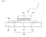
- FIG. 1 is a schematic cross-sectional view that shows a storage unit 1 (non-volatile memory) of first Embodiment in accordance with the first aspect of the present invention
- the semiconductor storage unit 1 has a structure in which a base insulating film 102 is formed on an insulating substrate 101 and a semiconductor layer 117 is formed on the base insulating film 102 .
- Two diffusion layer regions 112 and 113 functioning as a source region and a drain region are formed on the semiconductor layer 117 , with a body region 111 interposed therebetween.
- a gate insulating film 121 which forms the featured portion of the present invention, is laminated on the semiconductor layer 117 , and a gate electrode 131 is formed thereon in this order.
- the interface portion between the body region 111 and the gate insulating film 121 is an area that forms an inverted layer when the transistor is in the on-state, that is, a so-called channel region.
- the semiconductor storage unit of first Embodiment of the present invention is designed so that a current flowing between the two diffusion layer regions is changed depending on the quantity of charge accumulated in the gate insulating film 121 .
- any substrate may be used as the insulating substrate 101 as long as it has an insulating property, and, for example, a glass substrate, a ceramic substrate, an alumina substrate, or a resin substrate may be used.
- the substrate can be used as a display such as a light-transmitting type liquid crystal panel; therefore, a glass substrate and a transparent resin substrate are preferably used.
- a resin substrate is preferably used because the substrate becomes flexible, a light-weight substrate is achieved and the impact-resistant property can be easily improved.
- the base insulating film 102 is not necessarily required. However, in the case when a glass substrate is used as the insulating substrate 101 , a silicon oxide film, a silicon acid nitride film, a silicon nitride film or a laminated film of these may be preferably used. In this case, it is possible to prevent devices formed on the glass substrate from being contaminated with impurities scattered from the glass substrate.
- the semiconductor layer 117 may be made from, for example, amorphous silicon, polysilicon, or monocrystal silicon. In addition to these, semiconductor materials, such as silicon germanium and germanium, may be used.
- the semiconductor layer 117 made from any of these materials is preferably formed to have a thickness of, for example, 30 nm to 150 nm, so as to exert a memory effect in cooperation with the gate insulating film containing carbon atoms.
- the thickness of less than 30 nm makes it difficult to maintain the evenness of the film thickness, and the thickness exceeding 150 nm tends to fail to form holes completely upon operation of the transistor, resulting in degradation in characteristics.
- the thickness of the semiconductor layer 117 is preferably from 50 nm to 100 nm, more preferably, from 60 nm to 80 nm.
- the two diffusion layer regions 112 and 113 are N-channel-type conductive regions.
- the two diffusion layer regions 112 and 113 are P-channel-type conductive regions.
- the body region 111 is preferably prepared as a P-type conductive region or as an intrinsic region.
- the P-channel type semiconductor storage unit 1 it is preferably prepared as an N-type conductive region or as an intrinsic region.
- the gate insulating film 121 formed on the channel region inside the semiconductor layer 117 , is made of a silicon oxide film containing carbon atoms of 0.1 atomic percent of more.
- the silicon oxide film containing carbon atoms of about 0.1 atomic percent or more is allowed to accumulate charge, and exerts a remarkable memory effect.
- the rate of carbon atoms contained in the gate insulating film 121 is preferably set in a range from 0.1 atomic percent or more to 5.0 atomic percents or less.
- the rate of carbon atoms contained in the gate insulating film can be quantitatively analyzed by an SIMS process (secondary ion mass spectrometry) or an XPS process (X-ray photoelectric spectral analysis).
- the rate of carbon atoms is preferably set to 2.0 to 4.0 atomic percent, more preferably, to 2.5 to 4.0 atomic percent.
- a semiconductor storage unit including silicon oxide films containing carbon atoms of 3.0 atomic percent, 3.5 atomic percent and 4.0 atomic percent is allowed to exert a desirable memory effect.
- the thickness of the gate insulating film is preferably set in a range from 20 nm to 150 nm so as to allow the gate insulating film containing carbon atoms to exert a memory effect.
- the thickness of less than 20 nm fails to maintain the evenness of the film thickness, and causes an insufficient voltage resistance.
- the thickness exceeding 150 nm causes a very high threshold value, and also makes the on-current extremely small.
- the gate insulating film may be prepared either as a thermal oxide film or as a deposition film; however, in the present invention, a deposition film is preferably used.
- the film thickness of the gate insulating film is preferably set to 50 to 120 nm, more preferably, to 80 to 100 nm.
- a gate electrode 131 is formed on the gate insulating film 121 .
- examples of the material for the gate electrode 131 include metals such as W, Ta, Al, TaN and TaAlN, and semiconductors, such as amorphous silicon and polysilicon.
- the semiconductor storage unit in accordance with first Embodiment of the present invention may be formed by virtually the same processes as those used for manufacturing a normal thin-film transistor (TFT).
- TFT thin-film transistor
- a CVD (chemical vapor deposition) method in which tetraethoxysilane (TEOS) is introduced with the substrate temperature being set to 500° C.
- TEOS tetraethoxysilane
- the concentration of oxygen to be introduced upon carrying out the CVD method may be lowered, or the substrate temperature during the CVD method may be lowered.
- the reversed process may be carried out.
- FIG. 2 is a graph that shows threshold-value fluctuation characteristics of the first writing method and the first erasing method.
- the axis of abscissas represents the time (see) and the axis of ordinates represents the threshold value (V).
- the first writing method and the first erasing method respectively relate to electron injection and hole injection caused by FN tunnel.
- the semiconductor storage unit that has obtained the characteristic of FIG. 2 is of the N-channel type. That of the P-channel type can obtain virtually the same results as well.
- the gate insulating film is made from a silicon oxide film containing carbon atoms of 0.1 atomic percent, and has a thickness of 70 nm. Even when the gate insulating film contains carbon atoms of 0.1 atomic percent or more, the writing speed and the erasing speed do not become extremely fast. In other words, the threshold value fluctuation characteristic of FIG. 2 is also obtained in the case when the gate insulating film contains carbon atoms of 0.1 atomic percent or more. In contrast, in the case when the gate insulating film contains carbon atoms exceeding 5.0 atomic percent or more, this state is not desirable because the functions as the gate insulating film, such as a voltage resistant characteristic, deteriorate.
- Voltage conditions at the time of writing are +60V in the voltage (Vg) of the gate electrode and 0V in each of the voltage (Vs) of the source electrode, the voltage (Vd) of the drain electrode and the voltage (Vsub) in the body region.
- Voltage conditions at the time erasing are ⁇ 70V in the voltage (Vg) of the gate electrode and 0V in each of the voltage (Vs) of the source electrode, the voltage (Vd) of the drain electrode and the voltage (Vsub) in the body region.
- the above-mentioned voltages are only examples, and the present embodiment is not intended to be limited thereby.
- the curve above a dotted line in the center indicates changes in the threshold value upon carrying out a writing operation in accordance with the first writing method.
- the curve below the dotted line in the center indicates changes in the threshold value upon carrying out an erasing operation in accordance with the first erasing method.
- the semiconductor storage unit of first Embodiment prepared with a silicon oxide film containing carbon atoms of 0.1 atomic percent or more, is clearly allowed to exert a memory effect.
- FIG. 3 is a graph that shows threshold-value fluctuation characteristics obtained upon carrying out a writing process and an erasing process by applying an electric field having the same intensity to an element provided with a silicon oxide film containing no carbon atoms (below detection limit in SIMS), which forms a reference to the semiconductor storage unit of first Embodiment of the present invention.
- the axis of abscissas represents the time (see) and the axis of ordinates represents the threshold value (V).
- the same structure as that of the semiconductor storage unit of first Embodiment is used except that the silicon oxide film forming the gate insulating film contains no carbon atoms. As clearly shown by FIG. 3 , no memory effect is exerted.
- the key of the present invention is to use a silicon oxide film containing carbon atoms of 0.1 atomic percent or more as the gate insulating film, and this structure can be utilized as a non-volatile memory without the necessity of using an ONO film or the like in which a silicon nitride film is used.
- the rate of the carbon atoms may be increased to exceed 0.1 atomic percent.
- the functions as the gate insulating film extremely deteriorate so that the rate of carbon atoms contained in the silicon oxide film is preferably set in a range from 0.1 atomic percent or more to 5.0 atomic percents or less.
- the gate insulating film functioning as a memory storage unit is made of a single layer silicon oxide film containing carbon atoms of 0.1 atomic percent or more. Therefore, in comparison with a conventional art semiconductor storage unit in which a gate insulating film having an ONO structure using a silicon nitride film is used as a memory storage unit, the element structure can be simplified and the number of processes required for the formation thereof can be reduced.
- the second writing and erasing methods make it possible to greatly reduce a voltage in comparison with that of the first writing and erasing methods.
- To reduce the voltage of the writing and erasing methods is very important for the present invention. The reason for this is explained as follows:
- the semiconductor storage unit of the present invention is characterized in that the gate insulating film is made of a silicon oxide film containing carbon atoms of 0.1 atomic percent or more.
- This gate insulating film can be formed by using a CVD method; however, such a gate insulating film has the disadvantage that the voltage resistance is slightly lower than that of a thermal oxide film used in a general LSI process. Consequently, in the first writing and erasing methods in which the FN tunnel phenomenon is utilized, the voltage at the time of writing and erasing processes becomes close to the voltage resistance of the silicon oxide film.
- FIGS. 4 and 5 are graphs that show a gate current at the time of application of a voltage to the gate electrode of the semiconductor storage unit (N-channel type) of first Embodiment used for the measurements of FIG. 2 .
- the axis of abscissas represents the gate voltage Vg (V) and the axis of ordinates represents the gate current Ig (A).
- Vg the gate voltage
- Ig the gate current
- FIG. 4 Upon application of a positive gate voltage ( FIG. 4 ), the gate insulating film gets ruptured at 69V to cause a large current to flow (no data of 69V or more is shown in the graph). This voltage is close to the applied voltage (60V) in the first writing method.
- FIGS. 6 (N-channel type) and 7 (P-channel type) the following description will discuss the second writing method of the semiconductor storage unit of first Embodiment of the present invention.
- a reference voltage (0V) is applied to a terminal 152 connected to one of the diffusion layer regions 112 with a voltage higher than the reference voltage (for example, +10V) being applied to a terminal 153 connected to the other diffusion layer region 113
- a voltage (for example, +15V) higher than the reference voltage is applied to a terminal 151 connected to the gate electrode 131 .
- a reference voltage (0V) is applied to a terminal 155 connected to one of the diffusion layer regions 115 with a voltage lower than the reference voltage (for example, ⁇ 10V) being applied to a terminal 156 connected to the other diffusion layer region 116
- a voltage (for example, ⁇ 15V) lower than the reference voltage is applied to the terminal 151 connected to the gate electrode 131 .
- FIGS. 8 and 9 are graphs that show threshold-value fluctuation characteristics upon carrying out the second writing method respectively on semiconductor storage units of the N-channel type and the P-channel type.
- the characteristics (in the case of the N-channel type), shown in FIG. 8 are obtained upon application of +20V to the terminal 151 connected to the gate electrode, with +11V being applied to the terminal 153 connected to the other diffusion layer region 113 , in the case of carbon atoms of 0.1 atomic percent.
- the second writing method (+20V or ⁇ 0V applied to the gate electrode) makes it possible to definitely achieve a low voltage in comparison with the first writing method (+60V applied to the gate electrode).
- the margin of the writing voltage for the voltage resistance of the gate insulating film is always made much greater. Therefore, the reliability of the semiconductor storage unit can be improved.
- the semiconductor storage unit of the present invention is preferably prepared as the P-channel type.
- the diffusion layer region has a conductive type of P-type so that by accumulating holes to the gate insulating film, a writing process is preferably carried out so as to reduce a current flowing between the two diffusion layer regions.
- the element of the N-channel type is used in most cases, and the fact that the P-channel type is desirably used forms the inherent feature of the present invention.
- FIGS. 10 N-channel type
- 11 P-channel type
- a reference voltage (0V) is applied to the terminal 152 connected to one of the diffusion layer regions 112 , with a voltage higher than the reference voltage (for example, +10V) being applied to a terminal 153 connected to the other diffusion layer region 113 , a voltage (for example, ⁇ 15V) lower than the reference voltage is applied to a terminal 151 connected to the gate electrode 131 , with the reference voltage (for example, 0V) being applied to a terminal 154 connected to the body region 111 .
- FIGS. 12 (N-channel type) and 13 (P-channel type) the following description will discuss the third erasing method of the semiconductor storage unit of first Embodiment of the present invention.
- a reference voltage (0V) is applied to the terminal 152 connected to one of the diffusion layer regions 112 with a voltage higher than the reference voltage (for example, +10V) being applied to a terminal 153 connected to the other diffusion layer region 113
- a voltage (for example, ⁇ 15V) lower than the reference voltage is applied to a terminal 151 connected to the gate electrode 131 , with a voltage (for example, ⁇ 5V) lower than the reference voltage being applied to a terminal 154 connected to the body region 111 .
- the third erasing method is different from the second erasing method in that a voltage lower than the reference voltage is applied to the terminal 154 connected to the body region 111 .
- a voltage lower than the reference voltage is applied to the terminal 154 connected to the body region 111 .
- high energy holes are generated within the body region 111 near the other diffusion layer region 113 so that holes 162 are injected into the gate insulating film 121 near the other diffusion layer region 113 ; thus, the reading current is increased.
- the above-mentioned voltages are only examples, and the present embodiment is not intended to be limited thereby.
- a reference voltage (0V) is applied to a terminal 155 connected to one of the diffusion layer regions 115 with a voltage lower than the reference voltage (for example, ⁇ 10V) being applied to a terminal 156 connected to the other diffusion layer region 116
- a voltage (for example, +15V) higher than the reference voltage is applied to the terminal 151 connected to the gate electrode 131 , with a voltage (for example, +5V) higher than the reference voltage being applied to a terminal 157 connected to the body region 114 .
- the third erasing method is different from the second erasing method in that a voltage higher than the reference voltage is applied to the terminal 157 connected to the body region 114 .
- a voltage higher than the reference voltage is applied to the terminal 157 connected to the body region 114 .
- high energy electrons are generated within the body region 114 near the other diffusion layer region 116 so that electrons 161 are injected into the gate insulating film 121 near the other diffusion layer region 116 ; thus, the reading current is increased.
- the above-mentioned voltages are only examples, and the present embodiment is not intended to be limited thereby.
- FIG. 14 is a graph that shows threshold-value fluctuation characteristics upon carrying out the second and third erasing methods on a semiconductor storage unit of the P-channel type.
- the characteristics, shown in FIG. 14 are obtained upon application of +20V to the terminal 151 connected to the gate electrode, with ⁇ 11V being applied to the terminal 156 connected to the other diffusion layer region 116 , in the case of 0.1 atomic percent of carbon atoms, with respect to each of the second and third erasing methods.
- +10V is also applied to the terminal 157 connected to the body region 114 .
- both of the second and third erasing methods make it possible to definitely achieve a low voltage in comparison with that of the first erasing method (the greatest absolute value of the voltage to be applied is 70V of the gate electrode).
- the greatest absolute value of the voltage to be applied is 70V of the gate electrode.
- the semiconductor storage unit of the present invention is preferably prepared as the P-channel type.
- the erasing process can be carried out by using a voltage that is much lower than that of the first erasing method.
- the third erasing method carries out the erasing process at a higher speed as clearly shown by FIG. 14 .
- the voltage applied to the body region is positive relative to the reference voltage, and this symbol is the same as the symbol of the voltage applied to the gate electrode. Therefore, by using the third erasing method, it becomes possible to carry out a high-speed erasing process, without the necessity of taking the voltage resistance of the gate insulating film into consideration.
- a charge is injected only into the gate insulating film near the other diffusion layer region.
- charges can be simultaneously injected into the gate insulating film near one of the diffusion regions as well as near the other diffusion region.
- a reference voltage (0V) may be applied to the terminal 154 connected to the body region 111 , with a higher voltage (for example, +10v) being applied to the terminals 152 and 153 respectively connected to one of the diffusion layer regions 112 and the other diffusion layer region 113 , while a voltage (for example, ⁇ 15V) lower than the reference voltage is being applied to the terminal 151 connected to the gate electrode 131 .
- the P-channel type all the symbols of the above-mentioned voltage conditions can be reversed.
- the following description will discuss a desirable reading method upon carrying out each of the second writing method, the second erasing method and the third erasing method.
- the following description will discuss the N-channel type structure in which electrons are injected (written) into the gate insulating film 121 near the other diffusion layer region 113 .
- a reference voltage (0V) is applied to the terminal 153 connected to the other diffusion layer region 113 , with a voltage (for example, +5V) higher than the reference voltage being applied to the terminal 152 connected to one of the diffusion layer regions 112 , while a voltage (for example, +10V) higher than the reference voltage is being applied to the terminal 151 connected to the gate electrode 131 .
- the above-mentioned voltages are only examples, and although not limited by these, it is necessary to suppress a voltage to such a level as not to exert writing. The same is true for the state in which holes are injected into the gate insulating film.
- all the symbols of the above-mentioned voltage conditions can be reversed.
- the voltages of the terminal 152 and the terminal 153 can be exchanged.
- the above-mentioned reading method corresponds to a method in which, when electrons or holes are injected into the gate insulating film near the other diffusion layer region 113 , one of the diffusion layer regions 112 is used as the drain, with the other diffusion layer region 113 being used as the source.
- a reading method By carrying out such a reading method, a charge, accumulated within the gate insulating film as stored information, can be detected with high response.
- FIG. 16 the following description will discuss a method for storing information of two bits by using the above-mentioned second writing method, second erasing method or third erasing method and reading method.
- electrons 171 in the case of N-channel type
- holes 172 in the case of P-channel type
- FIG. 16 simultaneously shows states in which in the case of the N-channel type, electrons 171 are injected to the right side of the gate insulating film 121 and in which in the case of the P-channel type, hole 172 are injected to the left side thereof.
- holes in the case of the N-channel type
- electrons in the case of the P-channel type
- the gate insulating film 121 near one of the diffusion layer regions 112 or near the other diffusion layer region 113 .
- charges can be independently accumulated into the gate insulating film near one of the diffusion layer regions 112 or near the other diffusion layer region 113 respectively.
- stored information on the desired one of the sides can be read selectively. The above-mentioned methods make it possible to store and read information of two bits. Since the semiconductor storage unit of the present invention can be two-bit operated, the storage capacity can be increased.
- a semiconductor device in accordance with the second aspect of the present invention is provided with a semiconductor layer formed on an insulating substrate; a non-volatile memory that has two diffusion layer regions forming a source region and a drain region, which are formed in the semiconductor layer, a channel region fixed between the two diffusion layer regions, a gate insulating film that is formed on the channel region, and made of a silicon oxide film containing carbon atoms of 0.1 to 5.0 atomic percent, and a gate electrode formed on the gate insulating film; and a field effect transistor that has two diffusion layer regions forming a source region and a drain region, which are formed in the semiconductor layer, a channel region fixed between the two diffusion layer regions, a region having a high concentration of impurities and a region having a low concentration of impurities that are respectively formed on each of the two diffusion layer regions, the region having a low concentration of impurities being made in contact with the region having a high concentration of impurities and the channel region, a gate insulating film formed on the channel region
- the semiconductor storage unit relating to the first aspect of the present invention and the field effect transistor having a structure similar to that of the semiconductor storage unit are formed on the same insulating substrate.
- each of the diffusion layer regions of the field effect transistor is constituted by a region having a high concentration of impurities and a region having a low concentration of impurities that is made in contact with the region having a high concentration of impurities and a channel region. Consequently, it becomes possible to effectively prevent the characteristics of the field effect transistor from fluctuating with time. Therefore, with the number of processes to be added being minimized, the switching element and the non-volatile memory element with high reliability can be easily installed in a mixed manner.
- a semiconductor device in accordance with second Embodiment has a structure in which a semiconductor storage unit (non-volatile memory) 1 and a semiconductor device (TFT element) 2 are mounted on the same insulating substrate 101 in a mixed manner. Since the semiconductor storage unit 1 has been explained in detail in the aforementioned first embodiment, the explanation thereof will be omitted.
- the semiconductor device 2 which is a switching element, is provided with a semiconductor layer formed on an insulating substrate, two diffusion layer regions forming a source region and a drain region, which are formed in the semiconductor layer, a channel region fixed between the two diffusion layer regions, a gate insulating film formed on a channel area and a gate electrode formed on the gate insulating film, and each of the two diffusion layer regions has a region having a high concentration of impurities and a region having a low concentration of impurities that is made in contact with the region having a high concentration of impurities and the channel region.
- the semiconductor layer of the semiconductor device 2 is composed of a body region 211 , regions 214 and 215 having a low concentration of impurities, and regions 212 and 213 having a high concentration of impurities.
- the channel region is formed in a region inside the body region 211 , which is made in contact with the gate insulating film 221 .
- the two diffusion layer regions are respectively formed by the regions 214 and 215 having a low concentration of impurities and the regions 212 and 213 having a high concentration of impurities, and the regions 214 and 215 having a low concentration of impurities are placed between the regions 212 , 213 having a high concentration of impurities and the channel region.
- a gate electrode 231 is placed on the gate insulating film 221 .
- the semiconductor device 2 differs from the semiconductor storage unit 1 in that the diffusion layer regions of the semiconductor device 2 are constituted by the regions 214 and 215 having a low concentration of impurities and the regions 212 and 213 having a high concentration of impurities. It also differs therefrom in that the gate insulating film 221 contains virtually no carbon atoms.
- the concentration of impurities of the regions 212 and 213 that have a high concentration of impurities may be respectively set, for example, in a range from 2 ⁇ 10 19 cm ⁇ 3 to 1 ⁇ 10 21 cm ⁇ 3 by using, for example, phosphorous atoms or arsenic atoms in the case of the N-channel type, as well as by using, for example, boron atoms in the case of the P-channel type.
- the concentration of impurities of the regions 214 and 215 that have a low concentration of impurities may be respectively set, for example, in a range from 1 ⁇ 10 17 cm ⁇ 3 to 1 ⁇ 10 19 cm ⁇ 3 by using, for example, phosphorous atoms or arsenic atoms in the case of the N-channel type, as well as by using, for example, boron atoms in the case of the P-channel type.
- the gate insulating film 221 may be made from the same material as that of the gate insulating film 121 of the semiconductor storage unit 1 , or may be made from a different material. However, the gate insulating film 121 and the gate insulating film 221 are preferably made from the same material (a silicon oxide film containing carbon atoms of 0.1 to 5.0 atomic percent, with the same film thickness). In this case, since the same process can be commonly used for forming the gate insulating films, the number of processes can be reduced.
- the semiconductor device 2 serving as a switching element may be used, for example, as a selection transistor to be placed for each of pixels in a display device, as transistors constituting a display driver, or as transistors constituting a logic circuit. Moreover, by installing the semiconductor storage unit 1 forming a non-volatile memory in a mixed manner, the semiconductor device of the present embodiment is allowed to exert higher functions and have a wider range of applications.
- the diffusion layer regions of the semiconductor device 2 are provided with the regions 214 , 215 having a low concentration of impurities formed between the regions 212 , 213 having a high concentration of impurities and the channel region, hot carriers hardly occur upon operation of the transistor. Therefore, it becomes possible to prevent the transistor characteristics from fluctuating with time. Consequently, even in the case when the gate oxide film of the semiconductor device 2 contains carbon atoms of 0.1 to 5.0 atomic percent, it is possible to prevent them from giving adverse effects to the transistor operations.
- injections of impurities for the regions 214 and 215 having a low concentration of impurities may be selectively carried out on the regions where the semiconductor device 2 is to be formed. In this manner, with the number of processes to be added being minimized, the switching element and the non-volatile memory element with high reliability can be easily installed in a mixed manner.
- FIG. 18 is a schematic cross-sectional view of a modified example of a semiconductor device of the present invention.
- the semiconductor device shown in FIG. 18 differs from the semiconductor device shown in FIG. 17 in that the regions 312 and 313 having a high concentration of impurities of the semiconductor device 3 serving as a switching element are offset from the gate electrode 331 (not overlapped therewith).
- reference numeral 311 represents a body region
- 314 and 315 represent regions having a low concentration of impurities
- 321 represents a gate insulating film
- 331 represents a gate electrode.
- the semiconductor device shown in FIG. 17 it is possible to provide a higher voltage resistance easily.
- the semiconductor device shown in FIG. 18 makes it possible to provide a smaller electrostatic capacitance to each of the gate electrode and diffusion layer regions; therefore, this is advantageously used for achieving high-speed operations and low power consumption.
- a display device in accordance with the third aspect of the present invention including: the non-volatile memory and the field effect transistor, that are formed on a panel substrate of the display device.
- the semiconductor storage unit of the present invention since the semiconductor storage unit of the present invention is formed on the panel substrate of the display device, the cost of the externally added part and the attaching cost of the externally added part can be reduced. Moreover, since the adjustment can be automatically carried out easily, the inspection cost can be reduced. Furthermore, since the semiconductor storage unit of the present invention simplifies the structure of the gate insulating film and reduces the number of processes required, it is advantageous in cutting costs.
- Third Embodiment of the present invention relates to a liquid crystal display provided with a semiconductor storage unit (non-volatile memory) as shown in first Embodiment.
- a semiconductor storage unit non-volatile memory
- JP-A No. 2000-19557 has proposed such a liquid crystal display provided with a semiconductor memory.
- data to be gamma-corrected are stored in a memory element.
- the liquid crystal display as shown in third Embodiment of the present invention is characterized by a display device having opposing electrodes that face pixel electrodes and a semiconductor storage unit shown in first Embodiment formed on a panel substrate of this liquid crystal display.
- the semiconductor storage unit is utilized as an element that stores image information to be supplied to a voltage generating circuit for applying a voltage to the opposing electrodes of the liquid crystal display.
- a signal line 412 is connected to the gate electrode of a pixel TFT 411 , and a signal line 413 is connected to one of the diffusion layer regions of the pixel TFT 411 , with a pixel electrode 414 being connected to the other diffusion layer region.
- the pixel electrode 414 is placed face to face with an opposing electrode 415 commonly used in the panel, with liquid crystal 416 interposed therebetween.
- a predetermined voltage generated by the voltage generating circuit 422 is applied to the opposing electrode 415 .
- the voltage to be generated by the voltage generating circuit 422 is determined based upon image information stored in a memory unit 421 provided with the semiconductor storage unit (non-volatile memory) of the present invention.
- the voltage to be generated in the voltage generating circuit 422 which is applied to the opposing electrode 415 so as to suppress flickering of the screen, needs to be adjusted for each panel.
- This voltage adjustment is generally carried out by adjusting a variable resistor externally added to the panel.
- the semiconductor storage unit (non-volatile memory) of third Embodiment of the present invention the cost of the externally added part and the attaching cost of the externally added part can be reduced. Moreover, since the adjustment can be automatically carried out easily, the inspection cost can be reduced. Furthermore, since the semiconductor storage unit (non-volatile memory) of the present invention simplifies the structure of the gate insulating film and reduces the number of processes required, it is advantageous in cutting costs.
- a liquid crystal display in accordance with the forth aspect of the present invention provided with a pixel electrode and an opposing electrode, including: a voltage output circuit which, upon input of digital information, outputs a voltage determined by the digital information to the opposing electrode; a DA converter that converts digital gradation data to an analog gradation signal; and a storage circuit used for storing data that define a correlation between voltages of the digital gradation data and the analog gradation signal, wherein each of the voltage output circuit and the DA converter comprises the field effect transistor formed on the panel substrate of the liquid crystal display device, and the storage circuit comprises the semiconductor storage unit formed on the panel substrate of the liquid crystal display device.
- the semiconductor storage unit of the present invention is formed on the panel substrate of the liquid crystal display, the cost of the externally added part and the attaching cost of the externally added part can be reduced. Moreover, since the adjustment can be automatically carried out easily, the inspection cost can be reduced. Furthermore, since the semiconductor storage unit of the present invention simplifies the structure of the gate insulating film and reduces the number of processes required, it is advantageous in cutting costs.
- Fourth Embodiment of the present invention relates to a display device provided with a semiconductor storage unit (non-volatile memory) and a semiconductor device (TFT) as shown in second Embodiment.
- a semiconductor storage unit non-volatile memory
- TFT semiconductor device
- a liquid crystal panel, an organic EL panel or the like may be used as the display device.
- This display device has a structure in which a voltage output circuit which, upon input of digital information, outputs a voltage determined by the digital information to the opposing electrode, and a DA converter which converts digital gradation data to an analog gradation signal are further formed on the panel substrate, and data that defines the correlation between the voltages of the digital gradation data and the analog gradation signal are stored in the semiconductor storage unit of the above-mentioned first Embodiment.
- the display device 4 is provided with a display data generating circuit 513 , which sends display data prepared as a digital signal to the DA converter 512 .
- the DA converter 512 converts the display data as the digital signal to an analog signal, and sends the signal to the display unit 515 through an output circuit 514 .
- the correlation needs to be adjusted for each panel.
- the correlation between the voltages of the digital gradation data and analog gradation signal is stored in the memory unit 511 provided with the semiconductor storage unit (non-volatile memory) of the present invention.
- the correlation between the voltages of the digital gradation data and the analog gradation signal is generally stored in a non-volatile memory chip externally added to the panel.
- the semiconductor storage unit (non-volatile memory) of the present invention By using the semiconductor storage unit (non-volatile memory) of the present invention, the cost of the externally added part and the attaching cost of the externally added part can be reduced. Moreover, since the adjustment can be automatically carried out easily, the inspection cost can be reduced. Furthermore, since the semiconductor storage unit (non-volatile memory) of the present invention simplifies the structure of the gate insulating film and reduces the number of processes required, it is advantageous in cutting costs.
- An image receiving apparatus in accordance with the fifth aspect of the present invention including: a display device; a receiving circuit for receiving an image signal; an image signal circuit that supplies the image signal received by the receiving circuit to the display device; and a storage circuit that stores data required for generating the image signal, wherein each of the receiving circuit and the image signal circuit includes the field effect transistor formed on the panel substrate of the liquid crystal display device, and the storage circuit includes the semiconductor storage unit formed on the panel substrate of the display device.
- Fifth Embodiment of the present invention relates to an image receiving apparatus that is provided with a display device having a semiconductor storage unit (non-volatile memory) and a semiconductor device (TFT) as shown in second Embodiment, and has a structure in which a receiving circuit for receiving an image signal, an image signal circuit used for supplying the image signal received by the receiving circuit to the display device and the semiconductor storage unit used for storing data required for generating the image signal are formed on the display device and the panel substrate of the display device.
- a receiving circuit for receiving an image signal an image signal circuit used for supplying the image signal received by the receiving circuit to the display device and the semiconductor storage unit used for storing data required for generating the image signal are formed on the display device and the panel substrate of the display device.
- an image receiving apparatus 5 is provided with a display device (liquid crystal display panel) 611 , a tuner 612 , a speaker 613 , a control unit 614 and an antenna terminal 615 .
- FIG. 21 shows a system that receives a radio signal by an antenna; however, in the case of receiving a signal through a cable, the antenna terminal is replaced by a cable connecting terminal, and the tuner is replaced by a signal receiving unit.
- the display device 611 is provided with the semiconductor storage unit (non-volatile memory) of the present invention.
- the non-volatile memory placed on the display device 611 , can store data such as a voltage value to be applied to the opposing electrode of the liquid crystal panel and the correlation between voltages of the digital gradation data and the analog gradation signal.
- a coded signal is sent to the display device, and by encoding the code in the display panel, information security can be enhanced, and in this case, the key of the code can be stored in the semiconductor storage unit installed in the display device.
- this display device in an image receiving apparatus, it becomes possible to achieve a highly functional image receiving apparatus at low costs.
Abstract
Description
Claims (11)
Applications Claiming Priority (2)
| Application Number | Priority Date | Filing Date | Title |
|---|---|---|---|
| JP2006318719A JP4852400B2 (en) | 2006-11-27 | 2006-11-27 | Semiconductor memory device, semiconductor device, display device, liquid crystal display device, and receiver |
| JP2006-318719 | 2006-11-27 |
Publications (2)
| Publication Number | Publication Date |
|---|---|
| US20080136757A1 US20080136757A1 (en) | 2008-06-12 |
| US8059080B2 true US8059080B2 (en) | 2011-11-15 |
Family
ID=39497388
Family Applications (1)
| Application Number | Title | Priority Date | Filing Date |
|---|---|---|---|
| US11/945,129 Active 2030-09-14 US8059080B2 (en) | 2006-11-27 | 2007-11-26 | Semiconductor storage unit, semiconductor device and display device as well as liquid crystal display and image receiving apparatus |
Country Status (3)
| Country | Link |
|---|---|
| US (1) | US8059080B2 (en) |
| JP (1) | JP4852400B2 (en) |
| KR (1) | KR101366551B1 (en) |
Families Citing this family (4)
| Publication number | Priority date | Publication date | Assignee | Title |
|---|---|---|---|---|
| JP2010098054A (en) * | 2008-10-15 | 2010-04-30 | Sharp Corp | Memory element, semiconductor storage device, display device, and portable electronic equipment |
| JP2012124367A (en) * | 2010-12-09 | 2012-06-28 | Lg Display Co Ltd | Oxide insulator film, oxide semiconductor thin film transistor element, and method of manufacturing the same |
| JP5834458B2 (en) * | 2011-04-13 | 2015-12-24 | 株式会社ニコン | Optical element manufacturing method and optical element |
| KR20200051884A (en) * | 2018-11-05 | 2020-05-14 | 삼성디스플레이 주식회사 | Carrier, apparatus for manufacturing a display apparatus having the same and method for manufacturing a display apparatus |
Citations (22)
| Publication number | Priority date | Publication date | Assignee | Title |
|---|---|---|---|---|
| US4376672A (en) * | 1981-10-26 | 1983-03-15 | Applied Materials, Inc. | Materials and methods for plasma etching of oxides and nitrides of silicon |
| JPH04754A (en) | 1989-12-19 | 1992-01-06 | Matsushita Electric Ind Co Ltd | Mos element for storage |
| JPH1187545A (en) | 1997-07-08 | 1999-03-30 | Sony Corp | Semiconductor non-volatile memory device and manufacture thereof |
| JP2000294662A (en) | 1999-04-08 | 2000-10-20 | Matsushita Electric Ind Co Ltd | Nonvolatile semiconductor memory element and its manufacture |
| US20010006843A1 (en) * | 1999-12-29 | 2001-07-05 | Park Dong Su | Method for forming a gate insulating film for semiconductor devices |
| US20010013853A1 (en) * | 1997-11-13 | 2001-08-16 | Seiji Suzuki | Liquid crystal display device and method of manufacturing the same |
| US20010019158A1 (en) * | 1999-11-15 | 2001-09-06 | Shimpei Tsujikawa | Semiconductor device having gate insulating film of silicon oxide and silicon nitride films |
| US20010025998A1 (en) * | 1997-03-25 | 2001-10-04 | Toshiba Corporation` | Semiconductor integrated circuit manufacturing method and device |
| US20010048147A1 (en) * | 1995-09-14 | 2001-12-06 | Hideki Mizuhara | Semiconductor devices passivation film |
| JP2001351995A (en) | 2000-06-08 | 2001-12-21 | Mitsubishi Electric Corp | Nonvolatile semiconductor memory device and semiconductor integrated circuit |
| US6432843B1 (en) * | 2000-11-30 | 2002-08-13 | Samsung Electronics Co., Ltd. | Methods of manufacturing integrated circuit devices in which a spin on glass insulation layer is dissolved so as to recess the spin on glass insulation layer from the upper surface of a pattern |
| US20020160622A1 (en) * | 1994-08-11 | 2002-10-31 | Shunpei Yamazaki | Methods of heat treatment and heat treatment apparatus for silicon oxide films |
| JP2003243620A (en) | 2002-02-21 | 2003-08-29 | Seiko Epson Corp | Manufacturing method of nonvolatile memory device and manufacturing method of semiconductor device |
| US20040175873A1 (en) * | 1992-02-25 | 2004-09-09 | Semiconductor Energy Laboratory Co., Ltd. | Semiconductor device and method of forming the same |
| JP2005079186A (en) | 2003-08-28 | 2005-03-24 | Sharp Corp | Fine particle containing body, its manufacturing method, memory function body, memory element, and electronic equipment |
| JP2006065995A (en) | 2004-08-30 | 2006-03-09 | Sharp Corp | Semiconductor memory device and electronic device |
| JP2006236556A (en) | 2005-01-28 | 2006-09-07 | Semiconductor Energy Lab Co Ltd | Storage device semiconductor device, and drive method therefor |
| US20070001945A1 (en) * | 2005-07-04 | 2007-01-04 | Semiconductor Energy Laboratory Co., Ltd. | Display device and driving method thereof |
| US7180095B2 (en) * | 2003-02-19 | 2007-02-20 | Hitachi Displays, Ltd. | Display device and manufacturing method thereof |
| US7425931B1 (en) * | 1995-02-16 | 2008-09-16 | Semiconductor Energy Laboratory Co. Ltd. | Display unit of a helmet or a vehicle or an airplane |
| US7564291B2 (en) * | 2004-04-26 | 2009-07-21 | Polymer Vision Limited | Threshold voltage adjustment in thin film transistors |
| US7791571B2 (en) * | 2004-04-22 | 2010-09-07 | Semiconductor Energy Laboratory Co., Ltd. | Light emitting device and driving method of the same |
Family Cites Families (13)
| Publication number | Priority date | Publication date | Assignee | Title |
|---|---|---|---|---|
| JPS5016481A (en) * | 1973-06-09 | 1975-02-21 | ||
| JP3169309B2 (en) * | 1994-09-07 | 2001-05-21 | シャープ株式会社 | Method for manufacturing thin film semiconductor device |
| JPH08130259A (en) * | 1994-11-01 | 1996-05-21 | Sony Corp | Semiconductor memory element |
| JP2006013534A (en) * | 1997-07-08 | 2006-01-12 | Sony Corp | Manufacturing method of semiconductor nonvolatile storage device |
| JP4761646B2 (en) * | 2000-04-27 | 2011-08-31 | 株式会社半導体エネルギー研究所 | Non-volatile memory |
| JP3479273B2 (en) * | 2000-09-21 | 2003-12-15 | Tdk株式会社 | Phosphor thin film manufacturing method and EL panel |
| JP2002231834A (en) * | 2001-02-02 | 2002-08-16 | Ricoh Co Ltd | Semiconductor memory |
| JP4263001B2 (en) * | 2003-03-06 | 2009-05-13 | アイファイヤー アイピー コーポレイション | Sputtering target |
| JP4480955B2 (en) * | 2003-05-20 | 2010-06-16 | シャープ株式会社 | Semiconductor memory device |
| US7663915B2 (en) * | 2004-02-10 | 2010-02-16 | Semiconductor Energy Laboratory Co., Ltd. | Nonvolatile memory |
| KR100642898B1 (en) * | 2004-07-21 | 2006-11-03 | 에스티마이크로일렉트로닉스 엔.브이. | Transistor of semiconductor device and mathod for manufacturing the same |
| JP5352040B2 (en) * | 2004-08-23 | 2013-11-27 | 株式会社半導体エネルギー研究所 | Method for manufacturing semiconductor device |
| KR100668330B1 (en) * | 2005-02-21 | 2007-01-12 | 삼성전자주식회사 | Nonvolatile memory device and fabrication method of the same |
-
2006
- 2006-11-27 JP JP2006318719A patent/JP4852400B2/en not_active Expired - Fee Related
-
2007
- 2007-11-26 US US11/945,129 patent/US8059080B2/en active Active
- 2007-11-27 KR KR1020070121192A patent/KR101366551B1/en active IP Right Grant
Patent Citations (23)
| Publication number | Priority date | Publication date | Assignee | Title |
|---|---|---|---|---|
| US4376672A (en) * | 1981-10-26 | 1983-03-15 | Applied Materials, Inc. | Materials and methods for plasma etching of oxides and nitrides of silicon |
| JPH04754A (en) | 1989-12-19 | 1992-01-06 | Matsushita Electric Ind Co Ltd | Mos element for storage |
| US20040175873A1 (en) * | 1992-02-25 | 2004-09-09 | Semiconductor Energy Laboratory Co., Ltd. | Semiconductor device and method of forming the same |
| US20020160622A1 (en) * | 1994-08-11 | 2002-10-31 | Shunpei Yamazaki | Methods of heat treatment and heat treatment apparatus for silicon oxide films |
| US7425931B1 (en) * | 1995-02-16 | 2008-09-16 | Semiconductor Energy Laboratory Co. Ltd. | Display unit of a helmet or a vehicle or an airplane |
| US20060199371A1 (en) * | 1995-09-14 | 2006-09-07 | Sanyo Electric Co., Ltd. | Semiconductor devices passivation film |
| US20010048147A1 (en) * | 1995-09-14 | 2001-12-06 | Hideki Mizuhara | Semiconductor devices passivation film |
| US20010025998A1 (en) * | 1997-03-25 | 2001-10-04 | Toshiba Corporation` | Semiconductor integrated circuit manufacturing method and device |
| JPH1187545A (en) | 1997-07-08 | 1999-03-30 | Sony Corp | Semiconductor non-volatile memory device and manufacture thereof |
| US20010013853A1 (en) * | 1997-11-13 | 2001-08-16 | Seiji Suzuki | Liquid crystal display device and method of manufacturing the same |
| JP2000294662A (en) | 1999-04-08 | 2000-10-20 | Matsushita Electric Ind Co Ltd | Nonvolatile semiconductor memory element and its manufacture |
| US20010019158A1 (en) * | 1999-11-15 | 2001-09-06 | Shimpei Tsujikawa | Semiconductor device having gate insulating film of silicon oxide and silicon nitride films |
| US20010006843A1 (en) * | 1999-12-29 | 2001-07-05 | Park Dong Su | Method for forming a gate insulating film for semiconductor devices |
| JP2001351995A (en) | 2000-06-08 | 2001-12-21 | Mitsubishi Electric Corp | Nonvolatile semiconductor memory device and semiconductor integrated circuit |
| US6432843B1 (en) * | 2000-11-30 | 2002-08-13 | Samsung Electronics Co., Ltd. | Methods of manufacturing integrated circuit devices in which a spin on glass insulation layer is dissolved so as to recess the spin on glass insulation layer from the upper surface of a pattern |
| JP2003243620A (en) | 2002-02-21 | 2003-08-29 | Seiko Epson Corp | Manufacturing method of nonvolatile memory device and manufacturing method of semiconductor device |
| US7180095B2 (en) * | 2003-02-19 | 2007-02-20 | Hitachi Displays, Ltd. | Display device and manufacturing method thereof |
| JP2005079186A (en) | 2003-08-28 | 2005-03-24 | Sharp Corp | Fine particle containing body, its manufacturing method, memory function body, memory element, and electronic equipment |
| US7791571B2 (en) * | 2004-04-22 | 2010-09-07 | Semiconductor Energy Laboratory Co., Ltd. | Light emitting device and driving method of the same |
| US7564291B2 (en) * | 2004-04-26 | 2009-07-21 | Polymer Vision Limited | Threshold voltage adjustment in thin film transistors |
| JP2006065995A (en) | 2004-08-30 | 2006-03-09 | Sharp Corp | Semiconductor memory device and electronic device |
| JP2006236556A (en) | 2005-01-28 | 2006-09-07 | Semiconductor Energy Lab Co Ltd | Storage device semiconductor device, and drive method therefor |
| US20070001945A1 (en) * | 2005-07-04 | 2007-01-04 | Semiconductor Energy Laboratory Co., Ltd. | Display device and driving method thereof |
Also Published As
| Publication number | Publication date |
|---|---|
| JP4852400B2 (en) | 2012-01-11 |
| KR101366551B1 (en) | 2014-02-25 |
| KR20080048002A (en) | 2008-05-30 |
| US20080136757A1 (en) | 2008-06-12 |
| JP2008135457A (en) | 2008-06-12 |
Similar Documents
| Publication | Publication Date | Title |
|---|---|---|
| US20230317741A1 (en) | Semiconductor device | |
| US6323515B1 (en) | Non-volatile memory and semiconductor device | |
| US8023042B2 (en) | Semiconductor device and method of manufacturing therefor | |
| KR100646737B1 (en) | A display device | |
| JP6192989B2 (en) | Light emitting device | |
| KR20180099725A (en) | Metal oxide films and semiconductor devices | |
| JP2004247436A (en) | Semiconductor memory, display device, and mobile apparatus | |
| US7489550B2 (en) | EEPROM and method of driving the same | |
| CN101425541B (en) | Semiconductor element and device using the same | |
| US8059080B2 (en) | Semiconductor storage unit, semiconductor device and display device as well as liquid crystal display and image receiving apparatus | |
| US7271799B2 (en) | Display driver, display device, and portable electronic apparatus | |
| JP2004348808A (en) | Semiconductor memory device, portable electronic equipment, method for controlling erase operation, and method for controlling program operation | |
| JP2004335056A (en) | Method of programming and erasing semiconductor memory having a plurality of memory cells | |
| JP2004342274A (en) | Semiconductor memory device, and portable electronic device provided with the same | |
| US20090073158A1 (en) | Semiconductor element and device using the same | |
| US7203118B2 (en) | Semiconductor storage device and mobile electronic device | |
| JP2004349349A (en) | Semiconductor storage device and portable electronic apparatus | |
| US7038282B2 (en) | Semiconductor storage device | |
| JP2004348805A (en) | Semiconductor memory device | |
| JP2004342276A (en) | Semiconductor memory device and its programming method | |
| JP2004349334A (en) | Semiconductor storage device and method of improving data retention thereof | |
| JP2007004911A (en) | Semiconductor memory apparatus | |
| JP2004342275A (en) | Programming method for nonvolatile memory device, semiconductor memory device, and portable electronic device provided with the same | |
| JP2010098054A (en) | Memory element, semiconductor storage device, display device, and portable electronic equipment | |
| JP2004342256A (en) | Semiconductor memory device and portable electronic equipment |
Legal Events
| Date | Code | Title | Description |
|---|---|---|---|
| AS | Assignment |
Owner name: SHARP KABUSHIKI KAISHA, JAPAN Free format text: ASSIGNMENT OF ASSIGNORS INTEREST;ASSIGNORS:IWATA, HIROSHI;SHIBATA, AKIHIDE;ADACHI, KOHICHIRO;AND OTHERS;REEL/FRAME:020531/0543;SIGNING DATES FROM 20071115 TO 20071120 Owner name: SHARP KABUSHIKI KAISHA, JAPAN Free format text: ASSIGNMENT OF ASSIGNORS INTEREST;ASSIGNORS:IWATA, HIROSHI;SHIBATA, AKIHIDE;ADACHI, KOHICHIRO;AND OTHERS;SIGNING DATES FROM 20071115 TO 20071120;REEL/FRAME:020531/0543 |
|
| STCF | Information on status: patent grant |
Free format text: PATENTED CASE |
|
| FEPP | Fee payment procedure |
Free format text: PAYOR NUMBER ASSIGNED (ORIGINAL EVENT CODE: ASPN); ENTITY STATUS OF PATENT OWNER: LARGE ENTITY |
|
| FEPP | Fee payment procedure |
Free format text: PAYOR NUMBER ASSIGNED (ORIGINAL EVENT CODE: ASPN); ENTITY STATUS OF PATENT OWNER: LARGE ENTITY Free format text: PAYER NUMBER DE-ASSIGNED (ORIGINAL EVENT CODE: RMPN); ENTITY STATUS OF PATENT OWNER: LARGE ENTITY |
|
| FPAY | Fee payment |
Year of fee payment: 4 |
|
| MAFP | Maintenance fee payment |
Free format text: PAYMENT OF MAINTENANCE FEE, 8TH YEAR, LARGE ENTITY (ORIGINAL EVENT CODE: M1552); ENTITY STATUS OF PATENT OWNER: LARGE ENTITY Year of fee payment: 8 |
|
| MAFP | Maintenance fee payment |
Free format text: PAYMENT OF MAINTENANCE FEE, 12TH YEAR, LARGE ENTITY (ORIGINAL EVENT CODE: M1553); ENTITY STATUS OF PATENT OWNER: LARGE ENTITY Year of fee payment: 12 |