US8030710B2 - Strained semiconductor device - Google Patents
Strained semiconductor device Download PDFInfo
- Publication number
- US8030710B2 US8030710B2 US12/411,602 US41160209A US8030710B2 US 8030710 B2 US8030710 B2 US 8030710B2 US 41160209 A US41160209 A US 41160209A US 8030710 B2 US8030710 B2 US 8030710B2
- Authority
- US
- United States
- Prior art keywords
- active region
- pmosfet
- film
- nmosfet
- silicon oxide
- Prior art date
- Legal status (The legal status is an assumption and is not a legal conclusion. Google has not performed a legal analysis and makes no representation as to the accuracy of the status listed.)
- Expired - Fee Related, expires
Links
Images


Classifications
-
- H—ELECTRICITY
- H10—SEMICONDUCTOR DEVICES; ELECTRIC SOLID-STATE DEVICES NOT OTHERWISE PROVIDED FOR
- H10B—ELECTRONIC MEMORY DEVICES
- H10B10/00—Static random access memory [SRAM] devices
-
- H—ELECTRICITY
- H10—SEMICONDUCTOR DEVICES; ELECTRIC SOLID-STATE DEVICES NOT OTHERWISE PROVIDED FOR
- H10B—ELECTRONIC MEMORY DEVICES
- H10B10/00—Static random access memory [SRAM] devices
- H10B10/12—Static random access memory [SRAM] devices comprising a MOSFET load element
-
- H—ELECTRICITY
- H10—SEMICONDUCTOR DEVICES; ELECTRIC SOLID-STATE DEVICES NOT OTHERWISE PROVIDED FOR
- H10D—INORGANIC ELECTRIC SEMICONDUCTOR DEVICES
- H10D30/00—Field-effect transistors [FET]
- H10D30/60—Insulated-gate field-effect transistors [IGFET]
- H10D30/791—Arrangements for exerting mechanical stress on the crystal lattice of the channel regions
- H10D30/792—Arrangements for exerting mechanical stress on the crystal lattice of the channel regions comprising applied insulating layers, e.g. stress liners
-
- H—ELECTRICITY
- H10—SEMICONDUCTOR DEVICES; ELECTRIC SOLID-STATE DEVICES NOT OTHERWISE PROVIDED FOR
- H10D—INORGANIC ELECTRIC SEMICONDUCTOR DEVICES
- H10D30/00—Field-effect transistors [FET]
- H10D30/60—Insulated-gate field-effect transistors [IGFET]
- H10D30/791—Arrangements for exerting mechanical stress on the crystal lattice of the channel regions
- H10D30/795—Arrangements for exerting mechanical stress on the crystal lattice of the channel regions being in lateral device isolation regions, e.g. STI
-
- H—ELECTRICITY
- H10—SEMICONDUCTOR DEVICES; ELECTRIC SOLID-STATE DEVICES NOT OTHERWISE PROVIDED FOR
- H10D—INORGANIC ELECTRIC SEMICONDUCTOR DEVICES
- H10D84/00—Integrated devices formed in or on semiconductor substrates that comprise only semiconducting layers, e.g. on Si wafers or on GaAs-on-Si wafers
- H10D84/01—Manufacture or treatment
- H10D84/0123—Integrating together multiple components covered by H10D12/00 or H10D30/00, e.g. integrating multiple IGBTs
- H10D84/0126—Integrating together multiple components covered by H10D12/00 or H10D30/00, e.g. integrating multiple IGBTs the components including insulated gates, e.g. IGFETs
- H10D84/0165—Integrating together multiple components covered by H10D12/00 or H10D30/00, e.g. integrating multiple IGBTs the components including insulated gates, e.g. IGFETs the components including complementary IGFETs, e.g. CMOS devices
- H10D84/0167—Manufacturing their channels
-
- H—ELECTRICITY
- H10—SEMICONDUCTOR DEVICES; ELECTRIC SOLID-STATE DEVICES NOT OTHERWISE PROVIDED FOR
- H10D—INORGANIC ELECTRIC SEMICONDUCTOR DEVICES
- H10D84/00—Integrated devices formed in or on semiconductor substrates that comprise only semiconducting layers, e.g. on Si wafers or on GaAs-on-Si wafers
- H10D84/01—Manufacture or treatment
- H10D84/0123—Integrating together multiple components covered by H10D12/00 or H10D30/00, e.g. integrating multiple IGBTs
- H10D84/0126—Integrating together multiple components covered by H10D12/00 or H10D30/00, e.g. integrating multiple IGBTs the components including insulated gates, e.g. IGFETs
- H10D84/0165—Integrating together multiple components covered by H10D12/00 or H10D30/00, e.g. integrating multiple IGBTs the components including insulated gates, e.g. IGFETs the components including complementary IGFETs, e.g. CMOS devices
- H10D84/0188—Manufacturing their isolation regions
-
- H—ELECTRICITY
- H10—SEMICONDUCTOR DEVICES; ELECTRIC SOLID-STATE DEVICES NOT OTHERWISE PROVIDED FOR
- H10D—INORGANIC ELECTRIC SEMICONDUCTOR DEVICES
- H10D84/00—Integrated devices formed in or on semiconductor substrates that comprise only semiconducting layers, e.g. on Si wafers or on GaAs-on-Si wafers
- H10D84/01—Manufacture or treatment
- H10D84/02—Manufacture or treatment characterised by using material-based technologies
- H10D84/03—Manufacture or treatment characterised by using material-based technologies using Group IV technology, e.g. silicon technology or silicon-carbide [SiC] technology
- H10D84/038—Manufacture or treatment characterised by using material-based technologies using Group IV technology, e.g. silicon technology or silicon-carbide [SiC] technology using silicon technology, e.g. SiGe
-
- H10P14/69433—
-
- H10W20/075—
-
- H10W74/147—
-
- H—ELECTRICITY
- H10—SEMICONDUCTOR DEVICES; ELECTRIC SOLID-STATE DEVICES NOT OTHERWISE PROVIDED FOR
- H10D—INORGANIC ELECTRIC SEMICONDUCTOR DEVICES
- H10D30/00—Field-effect transistors [FET]
- H10D30/01—Manufacture or treatment
- H10D30/021—Manufacture or treatment of FETs having insulated gates [IGFET]
- H10D30/0212—Manufacture or treatment of FETs having insulated gates [IGFET] using self-aligned silicidation
-
- H—ELECTRICITY
- H10—SEMICONDUCTOR DEVICES; ELECTRIC SOLID-STATE DEVICES NOT OTHERWISE PROVIDED FOR
- H10D—INORGANIC ELECTRIC SEMICONDUCTOR DEVICES
- H10D30/00—Field-effect transistors [FET]
- H10D30/01—Manufacture or treatment
- H10D30/021—Manufacture or treatment of FETs having insulated gates [IGFET]
- H10D30/0223—Manufacture or treatment of FETs having insulated gates [IGFET] having source and drain regions or source and drain extensions self-aligned to sides of the gate
- H10D30/0227—Manufacture or treatment of FETs having insulated gates [IGFET] having source and drain regions or source and drain extensions self-aligned to sides of the gate having both lightly-doped source and drain extensions and source and drain regions self-aligned to the sides of the gate, e.g. lightly-doped drain [LDD] MOSFET or double-diffused drain [DDD] MOSFET
Definitions
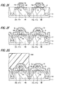
- An insulated gate electrode Gp formed of lamination of a gate insulating film and a gate electrode is formed on the active region AR 2 , and p-type source/drain extension regions EXp are formed in the n-type well NW on both sides of the insulated gate electrode.
Landscapes
- Metal-Oxide And Bipolar Metal-Oxide Semiconductor Integrated Circuits (AREA)
- Insulated Gate Type Field-Effect Transistor (AREA)
- Semiconductor Memories (AREA)
- Chemical Vapour Deposition (AREA)
- Element Separation (AREA)
- Internal Circuitry In Semiconductor Integrated Circuit Devices (AREA)
- Formation Of Insulating Films (AREA)
Applications Claiming Priority (2)
| Application Number | Priority Date | Filing Date | Title |
|---|---|---|---|
| JP2008167620A JP5163311B2 (ja) | 2008-06-26 | 2008-06-26 | 半導体装置及びその製造方法 |
| JP2008-167620 | 2008-06-26 |
Publications (2)
| Publication Number | Publication Date |
|---|---|
| US20090321840A1 US20090321840A1 (en) | 2009-12-31 |
| US8030710B2 true US8030710B2 (en) | 2011-10-04 |
Family
ID=41446347
Family Applications (1)
| Application Number | Title | Priority Date | Filing Date |
|---|---|---|---|
| US12/411,602 Expired - Fee Related US8030710B2 (en) | 2008-06-26 | 2009-03-26 | Strained semiconductor device |
Country Status (2)
| Country | Link |
|---|---|
| US (1) | US8030710B2 (ja) |
| JP (1) | JP5163311B2 (ja) |
Cited By (5)
| Publication number | Priority date | Publication date | Assignee | Title |
|---|---|---|---|---|
| US20120054711A1 (en) * | 2010-09-01 | 2012-03-01 | International Business Machines Corporation | Circuit analysis using transverse buckets |
| US20180047634A1 (en) * | 2016-08-11 | 2018-02-15 | Samsung Electronics Co., Ltd. | Semiconductor device including contact structure |
| US11337631B2 (en) | 2017-10-03 | 2022-05-24 | Brainn F.I.T. Imaging, LLC | Methods and magnetic imaging devices to inventory human brain cortical function |
| US11832966B2 (en) | 2019-04-03 | 2023-12-05 | Brain F.I.T. Imaging, LLC | Methods and magnetic imaging devices to inventory human brain cortical function |
| US11850058B2 (en) | 2016-03-30 | 2023-12-26 | Brain F.I.T. Imaging, LLC | Methods and magnetic imaging devices to inventory human brain cortical function |
Families Citing this family (9)
| Publication number | Priority date | Publication date | Assignee | Title |
|---|---|---|---|---|
| US8218353B1 (en) * | 2009-09-16 | 2012-07-10 | Altera Corporation | Memory element circuitry with stressed transistors |
| DE102010038746B4 (de) | 2010-07-30 | 2013-11-14 | GLOBALFOUNDRIES Dresden Module One Ltd. Liability Company & Co. KG | Verfahren zum Reduzieren der Topographie in Isolationsgebieten eines Halbleiterbauelements durch Anwenden einer Abscheide/Ätzsequenz vor der Herstellung des Zwischenschichtdielektrikums |
| US8378428B2 (en) * | 2010-09-29 | 2013-02-19 | Taiwan Semiconductor Manufacturing Company, Ltd. | Metal gate structure of a semiconductor device |
| CN102881694A (zh) | 2011-07-14 | 2013-01-16 | 中国科学院微电子研究所 | 半导体器件及其制造方法 |
| CN106910739B (zh) * | 2015-12-21 | 2022-01-11 | 三星电子株式会社 | 半导体器件 |
| KR102375583B1 (ko) * | 2015-12-21 | 2022-03-16 | 삼성전자주식회사 | 반도체 장치 및 이의 제조 방법 |
| US10043903B2 (en) * | 2015-12-21 | 2018-08-07 | Samsung Electronics Co., Ltd. | Semiconductor devices with source/drain stress liner |
| FR3100084B1 (fr) * | 2019-08-23 | 2021-10-01 | Commissariat Energie Atomique | procédé de fabrication de composants micro-électroniques |
| US11450573B2 (en) * | 2020-06-17 | 2022-09-20 | Globalfoundries U.S. Inc. | Structure with different stress-inducing isolation dielectrics for different polarity FETs |
Citations (5)
| Publication number | Priority date | Publication date | Assignee | Title |
|---|---|---|---|---|
| JP2003086708A (ja) | 2000-12-08 | 2003-03-20 | Hitachi Ltd | 半導体装置及びその製造方法 |
| US20050285137A1 (en) * | 2004-06-29 | 2005-12-29 | Fujitsu Limited | Semiconductor device with strain |
| US20070204250A1 (en) * | 2006-02-27 | 2007-08-30 | Synopsys, Inc. | Stress-managed revision of integrated circuit layouts |
| US20080054366A1 (en) | 2006-09-06 | 2008-03-06 | Fujitsu Limited | CMOS semiconductor device having tensile and compressive stress films |
| US20080237733A1 (en) * | 2007-03-27 | 2008-10-02 | International Business Machines Corporation | Structure and method to enhance channel stress by using optimized sti stress and nitride capping layer stress |
Family Cites Families (6)
| Publication number | Priority date | Publication date | Assignee | Title |
|---|---|---|---|---|
| JP4173658B2 (ja) * | 2001-11-26 | 2008-10-29 | 株式会社ルネサステクノロジ | 半導体装置及びその製造方法 |
| JP4369379B2 (ja) * | 2005-02-18 | 2009-11-18 | 富士通マイクロエレクトロニクス株式会社 | 半導体装置 |
| JP2006278754A (ja) * | 2005-03-29 | 2006-10-12 | Fujitsu Ltd | 半導体装置及びその製造方法 |
| JP4515951B2 (ja) * | 2005-03-31 | 2010-08-04 | 富士通セミコンダクター株式会社 | 半導体装置及びその製造方法 |
| US7538002B2 (en) * | 2006-02-24 | 2009-05-26 | Freescale Semiconductor, Inc. | Semiconductor process integrating source/drain stressors and interlevel dielectric layer stressors |
| JP5114892B2 (ja) * | 2006-08-25 | 2013-01-09 | ソニー株式会社 | 半導体装置 |
-
2008
- 2008-06-26 JP JP2008167620A patent/JP5163311B2/ja not_active Expired - Fee Related
-
2009
- 2009-03-26 US US12/411,602 patent/US8030710B2/en not_active Expired - Fee Related
Patent Citations (9)
| Publication number | Priority date | Publication date | Assignee | Title |
|---|---|---|---|---|
| JP2003086708A (ja) | 2000-12-08 | 2003-03-20 | Hitachi Ltd | 半導体装置及びその製造方法 |
| US6982465B2 (en) | 2000-12-08 | 2006-01-03 | Renesas Technology Corp. | Semiconductor device with CMOS-field-effect transistors having improved drain current characteristics |
| US20050285137A1 (en) * | 2004-06-29 | 2005-12-29 | Fujitsu Limited | Semiconductor device with strain |
| JP2006013322A (ja) | 2004-06-29 | 2006-01-12 | Fujitsu Ltd | 半導体装置 |
| US7423330B2 (en) | 2004-06-29 | 2008-09-09 | Fujitsu Limited | Semiconductor device with strain |
| US20070204250A1 (en) * | 2006-02-27 | 2007-08-30 | Synopsys, Inc. | Stress-managed revision of integrated circuit layouts |
| US20080054366A1 (en) | 2006-09-06 | 2008-03-06 | Fujitsu Limited | CMOS semiconductor device having tensile and compressive stress films |
| JP2008066484A (ja) | 2006-09-06 | 2008-03-21 | Fujitsu Ltd | Cmos半導体装置とその製造方法 |
| US20080237733A1 (en) * | 2007-03-27 | 2008-10-02 | International Business Machines Corporation | Structure and method to enhance channel stress by using optimized sti stress and nitride capping layer stress |
Cited By (10)
| Publication number | Priority date | Publication date | Assignee | Title |
|---|---|---|---|---|
| US20120054711A1 (en) * | 2010-09-01 | 2012-03-01 | International Business Machines Corporation | Circuit analysis using transverse buckets |
| US8453100B2 (en) * | 2010-09-01 | 2013-05-28 | International Business Machines Corporation | Circuit analysis using transverse buckets |
| US11850058B2 (en) | 2016-03-30 | 2023-12-26 | Brain F.I.T. Imaging, LLC | Methods and magnetic imaging devices to inventory human brain cortical function |
| US12303285B2 (en) | 2016-03-30 | 2025-05-20 | Brain F.I.T. Imaging, LLC | Methods and magnetic imaging devices to inventory human brain cortical function |
| US20180047634A1 (en) * | 2016-08-11 | 2018-02-15 | Samsung Electronics Co., Ltd. | Semiconductor device including contact structure |
| US10153212B2 (en) * | 2016-08-11 | 2018-12-11 | Samsung Electronics Co., Ltd. | Semiconductor device including contact structure |
| US11094593B2 (en) | 2016-08-11 | 2021-08-17 | Samsung Electronics Co., Ltd. | Semiconductor device including contact structure |
| US11337631B2 (en) | 2017-10-03 | 2022-05-24 | Brainn F.I.T. Imaging, LLC | Methods and magnetic imaging devices to inventory human brain cortical function |
| US11839475B2 (en) | 2017-10-03 | 2023-12-12 | Brain F.I.T. Imaging, LLC | Methods and magnetic imaging devices to inventory human brain cortical function |
| US11832966B2 (en) | 2019-04-03 | 2023-12-05 | Brain F.I.T. Imaging, LLC | Methods and magnetic imaging devices to inventory human brain cortical function |
Also Published As
| Publication number | Publication date |
|---|---|
| US20090321840A1 (en) | 2009-12-31 |
| JP5163311B2 (ja) | 2013-03-13 |
| JP2010010371A (ja) | 2010-01-14 |
Similar Documents
| Publication | Publication Date | Title |
|---|---|---|
| US8030710B2 (en) | Strained semiconductor device | |
| US12439630B2 (en) | Semiconductor component and manufacturing method thereof | |
| US7262472B2 (en) | Semiconductor device having stress and its manufacture method | |
| US8102030B2 (en) | Semiconductor device with strain | |
| US8648422B2 (en) | Semiconductor device with hetero junction | |
| US7652346B2 (en) | Semiconductor device and manufacturing method thereof | |
| US20120280291A1 (en) | Semiconductor device including gate openings | |
| US8106467B2 (en) | Semiconductor device having carrier mobility raised by generating strain in channel region | |
| CN101369598A (zh) | 半导体结构 | |
| US20070181950A1 (en) | Semiconductor device and its manufacturing method capable of suppressing junction leakage current | |
| JP2010267814A (ja) | 半導体装置及びその製造方法 | |
| US7737495B2 (en) | Semiconductor device having inter-layers with stress levels corresponding to the transistor type | |
| CN100576547C (zh) | 具有拉应力膜和压应力膜的cmos半导体器件 | |
| JP2007123518A (ja) | 半導体装置およびその製造方法 | |
| US7781844B2 (en) | Semiconductor device having a stressor film | |
| US20070278589A1 (en) | Semiconductor device and fabrication method thereof | |
| US20050156199A1 (en) | Method of forming a CMOS device | |
| KR20090020847A (ko) | 스트레인드 채널을 갖는 모스 트랜지스터의 제조 방법 및그에 의해 제조된 모스 트랜지스터 | |
| JP2010098157A (ja) | 半導体装置の製造方法 | |
| CN100479120C (zh) | 金属氧化物半导体晶体管及其制造方法 | |
| JP5454130B2 (ja) | 半導体およびその製造方法 | |
| US7060567B1 (en) | Method for fabricating trench power MOSFET | |
| JP2006060175A (ja) | 半導体装置及びその製造方法 | |
| JP2006351735A (ja) | Mos型トランジスタの製造方法及びmos型トランジスタ |
Legal Events
| Date | Code | Title | Description |
|---|---|---|---|
| AS | Assignment |
Owner name: FUJITSU MICROELECTRONICS LIMITED, JAPAN Free format text: ASSIGNMENT OF ASSIGNORS INTEREST;ASSIGNOR:PIDIN, SERGEY;REEL/FRAME:022463/0019 Effective date: 20090311 |
|
| AS | Assignment |
Owner name: FUJITSU SEMICONDUCTOR LIMITED, JAPAN Free format text: CHANGE OF NAME;ASSIGNOR:FUJITSU MICROELECTRONICS LIMITED;REEL/FRAME:024651/0744 Effective date: 20100401 |
|
| ZAAA | Notice of allowance and fees due |
Free format text: ORIGINAL CODE: NOA |
|
| ZAAB | Notice of allowance mailed |
Free format text: ORIGINAL CODE: MN/=. |
|
| STCF | Information on status: patent grant |
Free format text: PATENTED CASE |
|
| FEPP | Fee payment procedure |
Free format text: PAYOR NUMBER ASSIGNED (ORIGINAL EVENT CODE: ASPN); ENTITY STATUS OF PATENT OWNER: LARGE ENTITY |
|
| FPAY | Fee payment |
Year of fee payment: 4 |
|
| AS | Assignment |
Owner name: FUJITSU SEMICONDUCTOR LIMITED, JAPAN Free format text: CHANGE OF ADDRESS;ASSIGNOR:FUJITSU SEMICONDUCTOR LIMITED;REEL/FRAME:041188/0401 Effective date: 20160909 |
|
| MAFP | Maintenance fee payment |
Free format text: PAYMENT OF MAINTENANCE FEE, 8TH YEAR, LARGE ENTITY (ORIGINAL EVENT CODE: M1552); ENTITY STATUS OF PATENT OWNER: LARGE ENTITY Year of fee payment: 8 |
|
| FEPP | Fee payment procedure |
Free format text: MAINTENANCE FEE REMINDER MAILED (ORIGINAL EVENT CODE: REM.); ENTITY STATUS OF PATENT OWNER: LARGE ENTITY |
|
| LAPS | Lapse for failure to pay maintenance fees |
Free format text: PATENT EXPIRED FOR FAILURE TO PAY MAINTENANCE FEES (ORIGINAL EVENT CODE: EXP.); ENTITY STATUS OF PATENT OWNER: LARGE ENTITY |
|
| STCH | Information on status: patent discontinuation |
Free format text: PATENT EXPIRED DUE TO NONPAYMENT OF MAINTENANCE FEES UNDER 37 CFR 1.362 |
|
| FP | Lapsed due to failure to pay maintenance fee |
Effective date: 20231004 |