US8030710B2 - Strained semiconductor device - Google Patents
Strained semiconductor device Download PDFInfo
- Publication number
- US8030710B2 US8030710B2 US12/411,602 US41160209A US8030710B2 US 8030710 B2 US8030710 B2 US 8030710B2 US 41160209 A US41160209 A US 41160209A US 8030710 B2 US8030710 B2 US 8030710B2
- Authority
- US
- United States
- Prior art keywords
- active region
- pmosfet
- film
- nmosfet
- silicon oxide
- Prior art date
- Legal status (The legal status is an assumption and is not a legal conclusion. Google has not performed a legal analysis and makes no representation as to the accuracy of the status listed.)
- Expired - Fee Related, expires
Links
- 239000004065 semiconductor Substances 0.000 title claims abstract description 42
- VYPSYNLAJGMNEJ-UHFFFAOYSA-N Silicium dioxide Chemical compound O=[Si]=O VYPSYNLAJGMNEJ-UHFFFAOYSA-N 0.000 claims abstract description 59
- 229910052814 silicon oxide Inorganic materials 0.000 claims abstract description 59
- 238000002955 isolation Methods 0.000 claims abstract description 37
- 239000000758 substrate Substances 0.000 claims abstract description 28
- 229910052581 Si3N4 Inorganic materials 0.000 claims description 46
- HQVNEWCFYHHQES-UHFFFAOYSA-N silicon nitride Chemical compound N12[Si]34N5[Si]62N3[Si]51N64 HQVNEWCFYHHQES-UHFFFAOYSA-N 0.000 claims description 46
- 238000000034 method Methods 0.000 claims description 18
- 238000005530 etching Methods 0.000 claims description 13
- 238000004519 manufacturing process Methods 0.000 claims description 12
- 238000005268 plasma chemical vapour deposition Methods 0.000 claims description 3
- 238000002230 thermal chemical vapour deposition Methods 0.000 claims description 2
- 239000010408 film Substances 0.000 claims 37
- 239000013039 cover film Substances 0.000 claims 6
- 239000010410 layer Substances 0.000 description 17
- XUIMIQQOPSSXEZ-UHFFFAOYSA-N Silicon Chemical compound [Si] XUIMIQQOPSSXEZ-UHFFFAOYSA-N 0.000 description 14
- 229910052710 silicon Inorganic materials 0.000 description 14
- 239000010703 silicon Substances 0.000 description 14
- 150000002500 ions Chemical class 0.000 description 13
- 239000012535 impurity Substances 0.000 description 9
- 238000003475 lamination Methods 0.000 description 6
- BLRPTPMANUNPDV-UHFFFAOYSA-N Silane Chemical compound [SiH4] BLRPTPMANUNPDV-UHFFFAOYSA-N 0.000 description 5
- 238000009792 diffusion process Methods 0.000 description 5
- 239000007789 gas Substances 0.000 description 5
- 150000004767 nitrides Chemical class 0.000 description 5
- 238000001020 plasma etching Methods 0.000 description 5
- 230000008569 process Effects 0.000 description 5
- 229910021332 silicide Inorganic materials 0.000 description 5
- FVBUAEGBCNSCDD-UHFFFAOYSA-N silicide(4-) Chemical group [Si-4] FVBUAEGBCNSCDD-UHFFFAOYSA-N 0.000 description 5
- IJGRMHOSHXDMSA-UHFFFAOYSA-N Atomic nitrogen Chemical compound N#N IJGRMHOSHXDMSA-UHFFFAOYSA-N 0.000 description 4
- 230000001133 acceleration Effects 0.000 description 4
- 230000000052 comparative effect Effects 0.000 description 4
- 239000011229 interlayer Substances 0.000 description 4
- 238000005259 measurement Methods 0.000 description 4
- 125000006850 spacer group Chemical group 0.000 description 4
- 238000000151 deposition Methods 0.000 description 3
- 230000008021 deposition Effects 0.000 description 3
- 230000006870 function Effects 0.000 description 3
- 239000000203 mixture Substances 0.000 description 3
- 229910021420 polycrystalline silicon Inorganic materials 0.000 description 3
- 229920005591 polysilicon Polymers 0.000 description 3
- XPDWGBQVDMORPB-UHFFFAOYSA-N Fluoroform Chemical compound FC(F)F XPDWGBQVDMORPB-UHFFFAOYSA-N 0.000 description 2
- PXHVJJICTQNCMI-UHFFFAOYSA-N Nickel Chemical compound [Ni] PXHVJJICTQNCMI-UHFFFAOYSA-N 0.000 description 2
- BOTDANWDWHJENH-UHFFFAOYSA-N Tetraethyl orthosilicate Chemical compound CCO[Si](OCC)(OCC)OCC BOTDANWDWHJENH-UHFFFAOYSA-N 0.000 description 2
- 230000008901 benefit Effects 0.000 description 2
- 239000000969 carrier Substances 0.000 description 2
- 239000012159 carrier gas Substances 0.000 description 2
- 238000005229 chemical vapour deposition Methods 0.000 description 2
- 230000000295 complement effect Effects 0.000 description 2
- 230000000694 effects Effects 0.000 description 2
- 239000002184 metal Substances 0.000 description 2
- 229910052751 metal Inorganic materials 0.000 description 2
- 229910052757 nitrogen Inorganic materials 0.000 description 2
- 238000000206 photolithography Methods 0.000 description 2
- 238000005498 polishing Methods 0.000 description 2
- 229910000077 silane Inorganic materials 0.000 description 2
- 239000000126 substance Substances 0.000 description 2
- 239000002344 surface layer Substances 0.000 description 2
- 229910003915 SiCl2H2 Inorganic materials 0.000 description 1
- 230000004075 alteration Effects 0.000 description 1
- 230000015572 biosynthetic process Effects 0.000 description 1
- 239000002800 charge carrier Substances 0.000 description 1
- 238000006243 chemical reaction Methods 0.000 description 1
- 239000000470 constituent Substances 0.000 description 1
- 238000007796 conventional method Methods 0.000 description 1
- 239000013078 crystal Substances 0.000 description 1
- 230000000593 degrading effect Effects 0.000 description 1
- MROCJMGDEKINLD-UHFFFAOYSA-N dichlorosilane Chemical compound Cl[SiH2]Cl MROCJMGDEKINLD-UHFFFAOYSA-N 0.000 description 1
- PZPGRFITIJYNEJ-UHFFFAOYSA-N disilane Chemical compound [SiH3][SiH3] PZPGRFITIJYNEJ-UHFFFAOYSA-N 0.000 description 1
- CJNBYAVZURUTKZ-UHFFFAOYSA-N hafnium(IV) oxide Inorganic materials O=[Hf]=O CJNBYAVZURUTKZ-UHFFFAOYSA-N 0.000 description 1
- 238000010438 heat treatment Methods 0.000 description 1
- 230000006872 improvement Effects 0.000 description 1
- 230000010354 integration Effects 0.000 description 1
- 238000005468 ion implantation Methods 0.000 description 1
- 239000000463 material Substances 0.000 description 1
- 229910052759 nickel Inorganic materials 0.000 description 1
- 229910021334 nickel silicide Inorganic materials 0.000 description 1
- RUFLMLWJRZAWLJ-UHFFFAOYSA-N nickel silicide Chemical compound [Ni]=[Si]=[Ni] RUFLMLWJRZAWLJ-UHFFFAOYSA-N 0.000 description 1
- 230000008520 organization Effects 0.000 description 1
- 230000003647 oxidation Effects 0.000 description 1
- 238000007254 oxidation reaction Methods 0.000 description 1
- 230000001590 oxidative effect Effects 0.000 description 1
- 238000004335 scaling law Methods 0.000 description 1
- 238000006467 substitution reaction Methods 0.000 description 1
- VEDJZFSRVVQBIL-UHFFFAOYSA-N trisilane Chemical compound [SiH3][SiH2][SiH3] VEDJZFSRVVQBIL-UHFFFAOYSA-N 0.000 description 1
Images


Classifications
-
- H—ELECTRICITY
- H01—ELECTRIC ELEMENTS
- H01L—SEMICONDUCTOR DEVICES NOT COVERED BY CLASS H10
- H01L21/00—Processes or apparatus adapted for the manufacture or treatment of semiconductor or solid state devices or of parts thereof
- H01L21/70—Manufacture or treatment of devices consisting of a plurality of solid state components formed in or on a common substrate or of parts thereof; Manufacture of integrated circuit devices or of parts thereof
- H01L21/77—Manufacture or treatment of devices consisting of a plurality of solid state components or integrated circuits formed in, or on, a common substrate
- H01L21/78—Manufacture or treatment of devices consisting of a plurality of solid state components or integrated circuits formed in, or on, a common substrate with subsequent division of the substrate into plural individual devices
- H01L21/82—Manufacture or treatment of devices consisting of a plurality of solid state components or integrated circuits formed in, or on, a common substrate with subsequent division of the substrate into plural individual devices to produce devices, e.g. integrated circuits, each consisting of a plurality of components
- H01L21/822—Manufacture or treatment of devices consisting of a plurality of solid state components or integrated circuits formed in, or on, a common substrate with subsequent division of the substrate into plural individual devices to produce devices, e.g. integrated circuits, each consisting of a plurality of components the substrate being a semiconductor, using silicon technology
- H01L21/8232—Field-effect technology
- H01L21/8234—MIS technology, i.e. integration processes of field effect transistors of the conductor-insulator-semiconductor type
- H01L21/8238—Complementary field-effect transistors, e.g. CMOS
- H01L21/823878—Complementary field-effect transistors, e.g. CMOS isolation region manufacturing related aspects, e.g. to avoid interaction of isolation region with adjacent structure
-
- H—ELECTRICITY
- H01—ELECTRIC ELEMENTS
- H01L—SEMICONDUCTOR DEVICES NOT COVERED BY CLASS H10
- H01L21/00—Processes or apparatus adapted for the manufacture or treatment of semiconductor or solid state devices or of parts thereof
- H01L21/02—Manufacture or treatment of semiconductor devices or of parts thereof
- H01L21/02104—Forming layers
- H01L21/02107—Forming insulating materials on a substrate
- H01L21/02109—Forming insulating materials on a substrate characterised by the type of layer, e.g. type of material, porous/non-porous, pre-cursors, mixtures or laminates
- H01L21/02112—Forming insulating materials on a substrate characterised by the type of layer, e.g. type of material, porous/non-porous, pre-cursors, mixtures or laminates characterised by the material of the layer
- H01L21/02123—Forming insulating materials on a substrate characterised by the type of layer, e.g. type of material, porous/non-porous, pre-cursors, mixtures or laminates characterised by the material of the layer the material containing silicon
- H01L21/0217—Forming insulating materials on a substrate characterised by the type of layer, e.g. type of material, porous/non-porous, pre-cursors, mixtures or laminates characterised by the material of the layer the material containing silicon the material being a silicon nitride not containing oxygen, e.g. SixNy or SixByNz
-
- H—ELECTRICITY
- H01—ELECTRIC ELEMENTS
- H01L—SEMICONDUCTOR DEVICES NOT COVERED BY CLASS H10
- H01L21/00—Processes or apparatus adapted for the manufacture or treatment of semiconductor or solid state devices or of parts thereof
- H01L21/02—Manufacture or treatment of semiconductor devices or of parts thereof
- H01L21/04—Manufacture or treatment of semiconductor devices or of parts thereof the devices having at least one potential-jump barrier or surface barrier, e.g. PN junction, depletion layer or carrier concentration layer
- H01L21/18—Manufacture or treatment of semiconductor devices or of parts thereof the devices having at least one potential-jump barrier or surface barrier, e.g. PN junction, depletion layer or carrier concentration layer the devices having semiconductor bodies comprising elements of Group IV of the Periodic System or AIIIBV compounds with or without impurities, e.g. doping materials
- H01L21/30—Treatment of semiconductor bodies using processes or apparatus not provided for in groups H01L21/20 - H01L21/26
- H01L21/31—Treatment of semiconductor bodies using processes or apparatus not provided for in groups H01L21/20 - H01L21/26 to form insulating layers thereon, e.g. for masking or by using photolithographic techniques; After treatment of these layers; Selection of materials for these layers
- H01L21/314—Inorganic layers
- H01L21/318—Inorganic layers composed of nitrides
- H01L21/3185—Inorganic layers composed of nitrides of siliconnitrides
-
- H—ELECTRICITY
- H01—ELECTRIC ELEMENTS
- H01L—SEMICONDUCTOR DEVICES NOT COVERED BY CLASS H10
- H01L21/00—Processes or apparatus adapted for the manufacture or treatment of semiconductor or solid state devices or of parts thereof
- H01L21/70—Manufacture or treatment of devices consisting of a plurality of solid state components formed in or on a common substrate or of parts thereof; Manufacture of integrated circuit devices or of parts thereof
- H01L21/71—Manufacture of specific parts of devices defined in group H01L21/70
- H01L21/768—Applying interconnections to be used for carrying current between separate components within a device comprising conductors and dielectrics
- H01L21/76801—Applying interconnections to be used for carrying current between separate components within a device comprising conductors and dielectrics characterised by the formation and the after-treatment of the dielectrics, e.g. smoothing
- H01L21/76829—Applying interconnections to be used for carrying current between separate components within a device comprising conductors and dielectrics characterised by the formation and the after-treatment of the dielectrics, e.g. smoothing characterised by the formation of thin functional dielectric layers, e.g. dielectric etch-stop, barrier, capping or liner layers
- H01L21/76832—Multiple layers
-
- H—ELECTRICITY
- H01—ELECTRIC ELEMENTS
- H01L—SEMICONDUCTOR DEVICES NOT COVERED BY CLASS H10
- H01L21/00—Processes or apparatus adapted for the manufacture or treatment of semiconductor or solid state devices or of parts thereof
- H01L21/70—Manufacture or treatment of devices consisting of a plurality of solid state components formed in or on a common substrate or of parts thereof; Manufacture of integrated circuit devices or of parts thereof
- H01L21/77—Manufacture or treatment of devices consisting of a plurality of solid state components or integrated circuits formed in, or on, a common substrate
- H01L21/78—Manufacture or treatment of devices consisting of a plurality of solid state components or integrated circuits formed in, or on, a common substrate with subsequent division of the substrate into plural individual devices
- H01L21/82—Manufacture or treatment of devices consisting of a plurality of solid state components or integrated circuits formed in, or on, a common substrate with subsequent division of the substrate into plural individual devices to produce devices, e.g. integrated circuits, each consisting of a plurality of components
- H01L21/822—Manufacture or treatment of devices consisting of a plurality of solid state components or integrated circuits formed in, or on, a common substrate with subsequent division of the substrate into plural individual devices to produce devices, e.g. integrated circuits, each consisting of a plurality of components the substrate being a semiconductor, using silicon technology
- H01L21/8232—Field-effect technology
- H01L21/8234—MIS technology, i.e. integration processes of field effect transistors of the conductor-insulator-semiconductor type
- H01L21/8238—Complementary field-effect transistors, e.g. CMOS
- H01L21/823807—Complementary field-effect transistors, e.g. CMOS with a particular manufacturing method of the channel structures, e.g. channel implants, halo or pocket implants, or channel materials
-
- H—ELECTRICITY
- H01—ELECTRIC ELEMENTS
- H01L—SEMICONDUCTOR DEVICES NOT COVERED BY CLASS H10
- H01L23/00—Details of semiconductor or other solid state devices
- H01L23/28—Encapsulations, e.g. encapsulating layers, coatings, e.g. for protection
- H01L23/31—Encapsulations, e.g. encapsulating layers, coatings, e.g. for protection characterised by the arrangement or shape
- H01L23/3157—Partial encapsulation or coating
- H01L23/3192—Multilayer coating
-
- H—ELECTRICITY
- H01—ELECTRIC ELEMENTS
- H01L—SEMICONDUCTOR DEVICES NOT COVERED BY CLASS H10
- H01L29/00—Semiconductor devices adapted for rectifying, amplifying, oscillating or switching, or capacitors or resistors with at least one potential-jump barrier or surface barrier, e.g. PN junction depletion layer or carrier concentration layer; Details of semiconductor bodies or of electrodes thereof ; Multistep manufacturing processes therefor
- H01L29/66—Types of semiconductor device ; Multistep manufacturing processes therefor
- H01L29/68—Types of semiconductor device ; Multistep manufacturing processes therefor controllable by only the electric current supplied, or only the electric potential applied, to an electrode which does not carry the current to be rectified, amplified or switched
- H01L29/76—Unipolar devices, e.g. field effect transistors
- H01L29/772—Field effect transistors
- H01L29/78—Field effect transistors with field effect produced by an insulated gate
- H01L29/7842—Field effect transistors with field effect produced by an insulated gate means for exerting mechanical stress on the crystal lattice of the channel region, e.g. using a flexible substrate
- H01L29/7843—Field effect transistors with field effect produced by an insulated gate means for exerting mechanical stress on the crystal lattice of the channel region, e.g. using a flexible substrate the means being an applied insulating layer
-
- H—ELECTRICITY
- H01—ELECTRIC ELEMENTS
- H01L—SEMICONDUCTOR DEVICES NOT COVERED BY CLASS H10
- H01L29/00—Semiconductor devices adapted for rectifying, amplifying, oscillating or switching, or capacitors or resistors with at least one potential-jump barrier or surface barrier, e.g. PN junction depletion layer or carrier concentration layer; Details of semiconductor bodies or of electrodes thereof ; Multistep manufacturing processes therefor
- H01L29/66—Types of semiconductor device ; Multistep manufacturing processes therefor
- H01L29/68—Types of semiconductor device ; Multistep manufacturing processes therefor controllable by only the electric current supplied, or only the electric potential applied, to an electrode which does not carry the current to be rectified, amplified or switched
- H01L29/76—Unipolar devices, e.g. field effect transistors
- H01L29/772—Field effect transistors
- H01L29/78—Field effect transistors with field effect produced by an insulated gate
- H01L29/7842—Field effect transistors with field effect produced by an insulated gate means for exerting mechanical stress on the crystal lattice of the channel region, e.g. using a flexible substrate
- H01L29/7846—Field effect transistors with field effect produced by an insulated gate means for exerting mechanical stress on the crystal lattice of the channel region, e.g. using a flexible substrate the means being located in the lateral device isolation region, e.g. STI
-
- H—ELECTRICITY
- H10—SEMICONDUCTOR DEVICES; ELECTRIC SOLID-STATE DEVICES NOT OTHERWISE PROVIDED FOR
- H10B—ELECTRONIC MEMORY DEVICES
- H10B10/00—Static random access memory [SRAM] devices
-
- H—ELECTRICITY
- H10—SEMICONDUCTOR DEVICES; ELECTRIC SOLID-STATE DEVICES NOT OTHERWISE PROVIDED FOR
- H10B—ELECTRONIC MEMORY DEVICES
- H10B10/00—Static random access memory [SRAM] devices
- H10B10/12—Static random access memory [SRAM] devices comprising a MOSFET load element
-
- H—ELECTRICITY
- H01—ELECTRIC ELEMENTS
- H01L—SEMICONDUCTOR DEVICES NOT COVERED BY CLASS H10
- H01L29/00—Semiconductor devices adapted for rectifying, amplifying, oscillating or switching, or capacitors or resistors with at least one potential-jump barrier or surface barrier, e.g. PN junction depletion layer or carrier concentration layer; Details of semiconductor bodies or of electrodes thereof ; Multistep manufacturing processes therefor
- H01L29/66—Types of semiconductor device ; Multistep manufacturing processes therefor
- H01L29/66007—Multistep manufacturing processes
- H01L29/66075—Multistep manufacturing processes of devices having semiconductor bodies comprising group 14 or group 13/15 materials
- H01L29/66227—Multistep manufacturing processes of devices having semiconductor bodies comprising group 14 or group 13/15 materials the devices being controllable only by the electric current supplied or the electric potential applied, to an electrode which does not carry the current to be rectified, amplified or switched, e.g. three-terminal devices
- H01L29/66409—Unipolar field-effect transistors
- H01L29/66477—Unipolar field-effect transistors with an insulated gate, i.e. MISFET
- H01L29/665—Unipolar field-effect transistors with an insulated gate, i.e. MISFET using self aligned silicidation, i.e. salicide
-
- H—ELECTRICITY
- H01—ELECTRIC ELEMENTS
- H01L—SEMICONDUCTOR DEVICES NOT COVERED BY CLASS H10
- H01L29/00—Semiconductor devices adapted for rectifying, amplifying, oscillating or switching, or capacitors or resistors with at least one potential-jump barrier or surface barrier, e.g. PN junction depletion layer or carrier concentration layer; Details of semiconductor bodies or of electrodes thereof ; Multistep manufacturing processes therefor
- H01L29/66—Types of semiconductor device ; Multistep manufacturing processes therefor
- H01L29/66007—Multistep manufacturing processes
- H01L29/66075—Multistep manufacturing processes of devices having semiconductor bodies comprising group 14 or group 13/15 materials
- H01L29/66227—Multistep manufacturing processes of devices having semiconductor bodies comprising group 14 or group 13/15 materials the devices being controllable only by the electric current supplied or the electric potential applied, to an electrode which does not carry the current to be rectified, amplified or switched, e.g. three-terminal devices
- H01L29/66409—Unipolar field-effect transistors
- H01L29/66477—Unipolar field-effect transistors with an insulated gate, i.e. MISFET
- H01L29/66568—Lateral single gate silicon transistors
- H01L29/66575—Lateral single gate silicon transistors where the source and drain or source and drain extensions are self-aligned to the sides of the gate
- H01L29/6659—Lateral single gate silicon transistors where the source and drain or source and drain extensions are self-aligned to the sides of the gate with both lightly doped source and drain extensions and source and drain self-aligned to the sides of the gate, e.g. lightly doped drain [LDD] MOSFET, double diffused drain [DDD] MOSFET
-
- H—ELECTRICITY
- H01—ELECTRIC ELEMENTS
- H01L—SEMICONDUCTOR DEVICES NOT COVERED BY CLASS H10
- H01L2924/00—Indexing scheme for arrangements or methods for connecting or disconnecting semiconductor or solid-state bodies as covered by H01L24/00
- H01L2924/0001—Technical content checked by a classifier
- H01L2924/0002—Not covered by any one of groups H01L24/00, H01L24/00 and H01L2224/00
-
- H—ELECTRICITY
- H01—ELECTRIC ELEMENTS
- H01L—SEMICONDUCTOR DEVICES NOT COVERED BY CLASS H10
- H01L2924/00—Indexing scheme for arrangements or methods for connecting or disconnecting semiconductor or solid-state bodies as covered by H01L24/00
- H01L2924/10—Details of semiconductor or other solid state devices to be connected
- H01L2924/11—Device type
- H01L2924/13—Discrete devices, e.g. 3 terminal devices
- H01L2924/1304—Transistor
- H01L2924/1306—Field-effect transistor [FET]
- H01L2924/13091—Metal-Oxide-Semiconductor Field-Effect Transistor [MOSFET]
Definitions
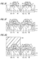
- An insulated gate electrode Gp formed of lamination of a gate insulating film and a gate electrode is formed on the active region AR 2 , and p-type source/drain extension regions EXp are formed in the n-type well NW on both sides of the insulated gate electrode.
Abstract
Description
Claims (11)
Applications Claiming Priority (2)
| Application Number | Priority Date | Filing Date | Title |
|---|---|---|---|
| JP2008167620A JP5163311B2 (en) | 2008-06-26 | 2008-06-26 | Semiconductor device and manufacturing method thereof |
| JP2008-167620 | 2008-06-26 |
Publications (2)
| Publication Number | Publication Date |
|---|---|
| US20090321840A1 US20090321840A1 (en) | 2009-12-31 |
| US8030710B2 true US8030710B2 (en) | 2011-10-04 |
Family
ID=41446347
Family Applications (1)
| Application Number | Title | Priority Date | Filing Date |
|---|---|---|---|
| US12/411,602 Expired - Fee Related US8030710B2 (en) | 2008-06-26 | 2009-03-26 | Strained semiconductor device |
Country Status (2)
| Country | Link |
|---|---|
| US (1) | US8030710B2 (en) |
| JP (1) | JP5163311B2 (en) |
Cited By (5)
| Publication number | Priority date | Publication date | Assignee | Title |
|---|---|---|---|---|
| US20120054711A1 (en) * | 2010-09-01 | 2012-03-01 | International Business Machines Corporation | Circuit analysis using transverse buckets |
| US20180047634A1 (en) * | 2016-08-11 | 2018-02-15 | Samsung Electronics Co., Ltd. | Semiconductor device including contact structure |
| US11337631B2 (en) | 2017-10-03 | 2022-05-24 | Brainn F.I.T. Imaging, LLC | Methods and magnetic imaging devices to inventory human brain cortical function |
| US11832966B2 (en) | 2019-04-03 | 2023-12-05 | Brain F.I.T. Imaging, LLC | Methods and magnetic imaging devices to inventory human brain cortical function |
| US11850058B2 (en) | 2016-03-30 | 2023-12-26 | Brain F.I.T. Imaging, LLC | Methods and magnetic imaging devices to inventory human brain cortical function |
Families Citing this family (9)
| Publication number | Priority date | Publication date | Assignee | Title |
|---|---|---|---|---|
| US8218353B1 (en) * | 2009-09-16 | 2012-07-10 | Altera Corporation | Memory element circuitry with stressed transistors |
| DE102010038746B4 (en) * | 2010-07-30 | 2013-11-14 | GLOBALFOUNDRIES Dresden Module One Ltd. Liability Company & Co. KG | A method for reducing the topography in isolation regions of a semiconductor device by applying a deposition / etch sequence prior to the formation of the interlayer dielectric |
| US8378428B2 (en) * | 2010-09-29 | 2013-02-19 | Taiwan Semiconductor Manufacturing Company, Ltd. | Metal gate structure of a semiconductor device |
| CN102881694A (en) * | 2011-07-14 | 2013-01-16 | 中国科学院微电子研究所 | Semiconductor device and manufacturing method therefor |
| CN106910739B (en) * | 2015-12-21 | 2022-01-11 | 三星电子株式会社 | Semiconductor device with a plurality of transistors |
| KR102375583B1 (en) * | 2015-12-21 | 2022-03-16 | 삼성전자주식회사 | Semiconductor device and method for fabricating the same |
| US10043903B2 (en) * | 2015-12-21 | 2018-08-07 | Samsung Electronics Co., Ltd. | Semiconductor devices with source/drain stress liner |
| FR3100084B1 (en) * | 2019-08-23 | 2021-10-01 | Commissariat Energie Atomique | microelectronic component manufacturing process |
| US11450573B2 (en) * | 2020-06-17 | 2022-09-20 | Globalfoundries U.S. Inc. | Structure with different stress-inducing isolation dielectrics for different polarity FETs |
Citations (5)
| Publication number | Priority date | Publication date | Assignee | Title |
|---|---|---|---|---|
| JP2003086708A (en) | 2000-12-08 | 2003-03-20 | Hitachi Ltd | Semiconductor device and manufacturing method thereof |
| US20050285137A1 (en) * | 2004-06-29 | 2005-12-29 | Fujitsu Limited | Semiconductor device with strain |
| US20070204250A1 (en) * | 2006-02-27 | 2007-08-30 | Synopsys, Inc. | Stress-managed revision of integrated circuit layouts |
| US20080054366A1 (en) | 2006-09-06 | 2008-03-06 | Fujitsu Limited | CMOS semiconductor device having tensile and compressive stress films |
| US20080237733A1 (en) * | 2007-03-27 | 2008-10-02 | International Business Machines Corporation | Structure and method to enhance channel stress by using optimized sti stress and nitride capping layer stress |
Family Cites Families (6)
| Publication number | Priority date | Publication date | Assignee | Title |
|---|---|---|---|---|
| JP4173658B2 (en) * | 2001-11-26 | 2008-10-29 | 株式会社ルネサステクノロジ | Semiconductor device and manufacturing method thereof |
| JP4369379B2 (en) * | 2005-02-18 | 2009-11-18 | 富士通マイクロエレクトロニクス株式会社 | Semiconductor device |
| JP2006278754A (en) * | 2005-03-29 | 2006-10-12 | Fujitsu Ltd | Semiconductor device and its manufacturing method |
| JP4515951B2 (en) * | 2005-03-31 | 2010-08-04 | 富士通セミコンダクター株式会社 | Semiconductor device and manufacturing method thereof |
| US7538002B2 (en) * | 2006-02-24 | 2009-05-26 | Freescale Semiconductor, Inc. | Semiconductor process integrating source/drain stressors and interlevel dielectric layer stressors |
| JP5114892B2 (en) * | 2006-08-25 | 2013-01-09 | ソニー株式会社 | Semiconductor device |
-
2008
- 2008-06-26 JP JP2008167620A patent/JP5163311B2/en not_active Expired - Fee Related
-
2009
- 2009-03-26 US US12/411,602 patent/US8030710B2/en not_active Expired - Fee Related
Patent Citations (9)
| Publication number | Priority date | Publication date | Assignee | Title |
|---|---|---|---|---|
| JP2003086708A (en) | 2000-12-08 | 2003-03-20 | Hitachi Ltd | Semiconductor device and manufacturing method thereof |
| US6982465B2 (en) | 2000-12-08 | 2006-01-03 | Renesas Technology Corp. | Semiconductor device with CMOS-field-effect transistors having improved drain current characteristics |
| US20050285137A1 (en) * | 2004-06-29 | 2005-12-29 | Fujitsu Limited | Semiconductor device with strain |
| JP2006013322A (en) | 2004-06-29 | 2006-01-12 | Fujitsu Ltd | Semiconductor device |
| US7423330B2 (en) | 2004-06-29 | 2008-09-09 | Fujitsu Limited | Semiconductor device with strain |
| US20070204250A1 (en) * | 2006-02-27 | 2007-08-30 | Synopsys, Inc. | Stress-managed revision of integrated circuit layouts |
| US20080054366A1 (en) | 2006-09-06 | 2008-03-06 | Fujitsu Limited | CMOS semiconductor device having tensile and compressive stress films |
| JP2008066484A (en) | 2006-09-06 | 2008-03-21 | Fujitsu Ltd | Cmos semiconductor device and its manufacturing method |
| US20080237733A1 (en) * | 2007-03-27 | 2008-10-02 | International Business Machines Corporation | Structure and method to enhance channel stress by using optimized sti stress and nitride capping layer stress |
Cited By (9)
| Publication number | Priority date | Publication date | Assignee | Title |
|---|---|---|---|---|
| US20120054711A1 (en) * | 2010-09-01 | 2012-03-01 | International Business Machines Corporation | Circuit analysis using transverse buckets |
| US8453100B2 (en) * | 2010-09-01 | 2013-05-28 | International Business Machines Corporation | Circuit analysis using transverse buckets |
| US11850058B2 (en) | 2016-03-30 | 2023-12-26 | Brain F.I.T. Imaging, LLC | Methods and magnetic imaging devices to inventory human brain cortical function |
| US20180047634A1 (en) * | 2016-08-11 | 2018-02-15 | Samsung Electronics Co., Ltd. | Semiconductor device including contact structure |
| US10153212B2 (en) * | 2016-08-11 | 2018-12-11 | Samsung Electronics Co., Ltd. | Semiconductor device including contact structure |
| US11094593B2 (en) | 2016-08-11 | 2021-08-17 | Samsung Electronics Co., Ltd. | Semiconductor device including contact structure |
| US11337631B2 (en) | 2017-10-03 | 2022-05-24 | Brainn F.I.T. Imaging, LLC | Methods and magnetic imaging devices to inventory human brain cortical function |
| US11839475B2 (en) | 2017-10-03 | 2023-12-12 | Brain F.I.T. Imaging, LLC | Methods and magnetic imaging devices to inventory human brain cortical function |
| US11832966B2 (en) | 2019-04-03 | 2023-12-05 | Brain F.I.T. Imaging, LLC | Methods and magnetic imaging devices to inventory human brain cortical function |
Also Published As
| Publication number | Publication date |
|---|---|
| JP2010010371A (en) | 2010-01-14 |
| JP5163311B2 (en) | 2013-03-13 |
| US20090321840A1 (en) | 2009-12-31 |
Similar Documents
| Publication | Publication Date | Title |
|---|---|---|
| US8030710B2 (en) | Strained semiconductor device | |
| US8106467B2 (en) | Semiconductor device having carrier mobility raised by generating strain in channel region | |
| US7262472B2 (en) | Semiconductor device having stress and its manufacture method | |
| US11848380B2 (en) | Semiconductor component and manufacturing method thereof | |
| US8102030B2 (en) | Semiconductor device with strain | |
| US7737495B2 (en) | Semiconductor device having inter-layers with stress levels corresponding to the transistor type | |
| US8648422B2 (en) | Semiconductor device with hetero junction | |
| JP5132928B2 (en) | Semiconductor device | |
| US20120280291A1 (en) | Semiconductor device including gate openings | |
| JP2008282901A (en) | Semiconductor device, and manufacturing method of semiconductor device | |
| US20050156199A1 (en) | Method of forming a CMOS device | |
| US20070181950A1 (en) | Semiconductor device and its manufacturing method capable of suppressing junction leakage current | |
| JP2010267814A (en) | Semiconductor device, and method of manufacturing the same | |
| US20080054366A1 (en) | CMOS semiconductor device having tensile and compressive stress films | |
| US7781844B2 (en) | Semiconductor device having a stressor film | |
| US20070278589A1 (en) | Semiconductor device and fabrication method thereof | |
| KR20090020847A (en) | Method of fabricating a mos transistor having a strained channel and mos transistor fabricated thereby | |
| JP2010098157A (en) | Process of fabricating semiconductor device | |
| US7060567B1 (en) | Method for fabricating trench power MOSFET | |
| JP2004039985A (en) | Semiconductor device and manufacturing method therefor | |
| JP5454130B2 (en) | Semiconductor and manufacturing method thereof | |
| JP2006060175A (en) | Semiconductor device and its manufacturing method | |
| JP2010004056A (en) | Method of manufacturing semiconductor device | |
| CN107968071A (en) | A kind of semiconductor devices and its manufacture method and electronic device | |
| JP2012248561A (en) | Semiconductor device and method of manufacturing the same |
Legal Events
| Date | Code | Title | Description |
|---|---|---|---|
| AS | Assignment |
Owner name: FUJITSU MICROELECTRONICS LIMITED, JAPAN Free format text: ASSIGNMENT OF ASSIGNORS INTEREST;ASSIGNOR:PIDIN, SERGEY;REEL/FRAME:022463/0019 Effective date: 20090311 |
|
| AS | Assignment |
Owner name: FUJITSU SEMICONDUCTOR LIMITED, JAPAN Free format text: CHANGE OF NAME;ASSIGNOR:FUJITSU MICROELECTRONICS LIMITED;REEL/FRAME:024651/0744 Effective date: 20100401 |
|
| ZAAA | Notice of allowance and fees due |
Free format text: ORIGINAL CODE: NOA |
|
| ZAAB | Notice of allowance mailed |
Free format text: ORIGINAL CODE: MN/=. |
|
| STCF | Information on status: patent grant |
Free format text: PATENTED CASE |
|
| FEPP | Fee payment procedure |
Free format text: PAYOR NUMBER ASSIGNED (ORIGINAL EVENT CODE: ASPN); ENTITY STATUS OF PATENT OWNER: LARGE ENTITY |
|
| FPAY | Fee payment |
Year of fee payment: 4 |
|
| AS | Assignment |
Owner name: FUJITSU SEMICONDUCTOR LIMITED, JAPAN Free format text: CHANGE OF ADDRESS;ASSIGNOR:FUJITSU SEMICONDUCTOR LIMITED;REEL/FRAME:041188/0401 Effective date: 20160909 |
|
| MAFP | Maintenance fee payment |
Free format text: PAYMENT OF MAINTENANCE FEE, 8TH YEAR, LARGE ENTITY (ORIGINAL EVENT CODE: M1552); ENTITY STATUS OF PATENT OWNER: LARGE ENTITY Year of fee payment: 8 |
|
| FEPP | Fee payment procedure |
Free format text: MAINTENANCE FEE REMINDER MAILED (ORIGINAL EVENT CODE: REM.); ENTITY STATUS OF PATENT OWNER: LARGE ENTITY |
|
| LAPS | Lapse for failure to pay maintenance fees |
Free format text: PATENT EXPIRED FOR FAILURE TO PAY MAINTENANCE FEES (ORIGINAL EVENT CODE: EXP.); ENTITY STATUS OF PATENT OWNER: LARGE ENTITY |
|
| STCH | Information on status: patent discontinuation |
Free format text: PATENT EXPIRED DUE TO NONPAYMENT OF MAINTENANCE FEES UNDER 37 CFR 1.362 |
|
| FP | Lapsed due to failure to pay maintenance fee |
Effective date: 20231004 |