US7948258B2 - Semiconductor arrangement and method for the measurement of a resistance - Google Patents
Semiconductor arrangement and method for the measurement of a resistance Download PDFInfo
- Publication number
- US7948258B2 US7948258B2 US12/406,721 US40672109A US7948258B2 US 7948258 B2 US7948258 B2 US 7948258B2 US 40672109 A US40672109 A US 40672109A US 7948258 B2 US7948258 B2 US 7948258B2
- Authority
- US
- United States
- Prior art keywords
- terminal
- area
- test
- contact
- contact area
- Prior art date
- Legal status (The legal status is an assumption and is not a legal conclusion. Google has not performed a legal analysis and makes no representation as to the accuracy of the status listed.)
- Expired - Fee Related, expires
Links
- 239000004065 semiconductor Substances 0.000 title claims abstract description 103
- 238000005259 measurement Methods 0.000 title claims abstract description 50
- 238000000034 method Methods 0.000 title claims abstract description 12
- 238000012360 testing method Methods 0.000 claims abstract description 161
- 229910000679 solder Inorganic materials 0.000 claims description 21
- 239000002184 metal Substances 0.000 claims description 10
- 230000015572 biosynthetic process Effects 0.000 claims description 8
- 239000004020 conductor Substances 0.000 claims description 5
- 101000872823 Xenopus laevis Probable histone deacetylase 1-A Proteins 0.000 abstract description 16
- 101000674731 Homo sapiens TGF-beta-activated kinase 1 and MAP3K7-binding protein 1 Proteins 0.000 abstract description 10
- 102100021228 TGF-beta-activated kinase 1 and MAP3K7-binding protein 1 Human genes 0.000 abstract description 10
- 239000000523 sample Substances 0.000 description 28
- 239000013256 coordination polymer Substances 0.000 description 7
- 230000006870 function Effects 0.000 description 7
- 230000003071 parasitic effect Effects 0.000 description 7
- 101000674728 Homo sapiens TGF-beta-activated kinase 1 and MAP3K7-binding protein 2 Proteins 0.000 description 6
- 102100021227 TGF-beta-activated kinase 1 and MAP3K7-binding protein 2 Human genes 0.000 description 6
- 238000004806 packaging method and process Methods 0.000 description 5
- XUIMIQQOPSSXEZ-UHFFFAOYSA-N Silicon Chemical compound [Si] XUIMIQQOPSSXEZ-UHFFFAOYSA-N 0.000 description 3
- 230000000694 effects Effects 0.000 description 3
- 229910052710 silicon Inorganic materials 0.000 description 3
- 239000010703 silicon Substances 0.000 description 3
- -1 for example Substances 0.000 description 2
- 239000000463 material Substances 0.000 description 2
- 238000012883 sequential measurement Methods 0.000 description 2
- QVGXLLKOCUKJST-UHFFFAOYSA-N atomic oxygen Chemical compound [O] QVGXLLKOCUKJST-UHFFFAOYSA-N 0.000 description 1
- 230000007547 defect Effects 0.000 description 1
- 230000005611 electricity Effects 0.000 description 1
- 238000004519 manufacturing process Methods 0.000 description 1
- 238000001465 metallisation Methods 0.000 description 1
- 230000001590 oxidative effect Effects 0.000 description 1
- 229910052760 oxygen Inorganic materials 0.000 description 1
- 239000001301 oxygen Substances 0.000 description 1
- 230000009993 protective function Effects 0.000 description 1
- 238000000926 separation method Methods 0.000 description 1
- 238000005476 soldering Methods 0.000 description 1
- 239000000126 substance Substances 0.000 description 1
- XLYOFNOQVPJJNP-UHFFFAOYSA-N water Substances O XLYOFNOQVPJJNP-UHFFFAOYSA-N 0.000 description 1
Images


Classifications
-
- G—PHYSICS
- G01—MEASURING; TESTING
- G01R—MEASURING ELECTRIC VARIABLES; MEASURING MAGNETIC VARIABLES
- G01R27/00—Arrangements for measuring resistance, reactance, impedance, or electric characteristics derived therefrom
- G01R27/02—Measuring real or complex resistance, reactance, impedance, or other two-pole characteristics derived therefrom, e.g. time constant
- G01R27/08—Measuring resistance by measuring both voltage and current
-
- G—PHYSICS
- G01—MEASURING; TESTING
- G01R—MEASURING ELECTRIC VARIABLES; MEASURING MAGNETIC VARIABLES
- G01R31/00—Arrangements for testing electric properties; Arrangements for locating electric faults; Arrangements for electrical testing characterised by what is being tested not provided for elsewhere
- G01R31/28—Testing of electronic circuits, e.g. by signal tracer
- G01R31/2851—Testing of integrated circuits [IC]
- G01R31/2853—Electrical testing of internal connections or -isolation, e.g. latch-up or chip-to-lead connections
-
- G—PHYSICS
- G01—MEASURING; TESTING
- G01R—MEASURING ELECTRIC VARIABLES; MEASURING MAGNETIC VARIABLES
- G01R27/00—Arrangements for measuring resistance, reactance, impedance, or electric characteristics derived therefrom
- G01R27/02—Measuring real or complex resistance, reactance, impedance, or other two-pole characteristics derived therefrom, e.g. time constant
- G01R27/20—Measuring earth resistance; Measuring contact resistance, e.g. of earth connections, e.g. plates
- G01R27/205—Measuring contact resistance of connections, e.g. of earth connections
-
- G—PHYSICS
- G01—MEASURING; TESTING
- G01R—MEASURING ELECTRIC VARIABLES; MEASURING MAGNETIC VARIABLES
- G01R31/00—Arrangements for testing electric properties; Arrangements for locating electric faults; Arrangements for electrical testing characterised by what is being tested not provided for elsewhere
- G01R31/26—Testing of individual semiconductor devices
- G01R31/27—Testing of devices without physical removal from the circuit of which they form part, e.g. compensating for effects surrounding elements
- G01R31/275—Testing of devices without physical removal from the circuit of which they form part, e.g. compensating for effects surrounding elements for testing individual semiconductor components within integrated circuits
-
- G—PHYSICS
- G01—MEASURING; TESTING
- G01R—MEASURING ELECTRIC VARIABLES; MEASURING MAGNETIC VARIABLES
- G01R31/00—Arrangements for testing electric properties; Arrangements for locating electric faults; Arrangements for electrical testing characterised by what is being tested not provided for elsewhere
- G01R31/28—Testing of electronic circuits, e.g. by signal tracer
- G01R31/2851—Testing of integrated circuits [IC]
- G01R31/2884—Testing of integrated circuits [IC] using dedicated test connectors, test elements or test circuits on the IC under test
-
- H—ELECTRICITY
- H01—ELECTRIC ELEMENTS
- H01L—SEMICONDUCTOR DEVICES NOT COVERED BY CLASS H10
- H01L22/00—Testing or measuring during manufacture or treatment; Reliability measurements, i.e. testing of parts without further processing to modify the parts as such; Structural arrangements therefor
- H01L22/30—Structural arrangements specially adapted for testing or measuring during manufacture or treatment, or specially adapted for reliability measurements
- H01L22/34—Circuits for electrically characterising or monitoring manufacturing processes, e. g. whole test die, wafers filled with test structures, on-board-devices incorporated on each die, process control monitors or pad structures thereof, devices in scribe line
-
- G—PHYSICS
- G01—MEASURING; TESTING
- G01R—MEASURING ELECTRIC VARIABLES; MEASURING MAGNETIC VARIABLES
- G01R31/00—Arrangements for testing electric properties; Arrangements for locating electric faults; Arrangements for electrical testing characterised by what is being tested not provided for elsewhere
- G01R31/50—Testing of electric apparatus, lines, cables or components for short-circuits, continuity, leakage current or incorrect line connections
- G01R31/66—Testing of connections, e.g. of plugs or non-disconnectable joints
- G01R31/70—Testing of connections between components and printed circuit boards
- G01R31/71—Testing of solder joints
-
- H—ELECTRICITY
- H01—ELECTRIC ELEMENTS
- H01L—SEMICONDUCTOR DEVICES NOT COVERED BY CLASS H10
- H01L2224/00—Indexing scheme for arrangements for connecting or disconnecting semiconductor or solid-state bodies and methods related thereto as covered by H01L24/00
- H01L2224/01—Means for bonding being attached to, or being formed on, the surface to be connected, e.g. chip-to-package, die-attach, "first-level" interconnects; Manufacturing methods related thereto
- H01L2224/10—Bump connectors; Manufacturing methods related thereto
- H01L2224/12—Structure, shape, material or disposition of the bump connectors prior to the connecting process
- H01L2224/13—Structure, shape, material or disposition of the bump connectors prior to the connecting process of an individual bump connector
Definitions
- the invention concerns a semiconductor arrangement and a method for the measurement, in particular, of a low resistance between two terminals.
- wafer-level package also called a chip-scale package
- a wafer-level package also called a chip-scale package
- solder balls are placed directly onto a silicon chip.
- This special packaging form is particularly space-saving.
- the measurement of low resistances of components, for example, transistors, in integrated circuits in the wafer-level package is of special importance in ensuring functionality and quality during product testing.
- values must thereby be measured in the order of magnitude of approximately 100 m ⁇ . This requirement appears frequently in circuits in which large currents flow and small losses are important, for example, in the areas of electricity supply, also called power management, or audio.
- the contacts which produce the link between the terminals of a component and a measuring device during a product test have a far higher contact resistance than does the actual component to be measured. Moreover, it is not the pure resistance of the component in silicon that is important to a user, but rather the total value of the resistance of a terminal of the component to the other terminal. Thus, the parasitic fractions of the packaging, or of the package, have to be taken into consideration. Because of the great variation in these contact resistances caused in production, it is not possible to account for the parasitic fractions with a constant correction.
- the four-wire measurement usually used, also known as the Kelvin measurement has serious problems in the area of wafer-level packages as a result of the particularly small contacts.
- One object of the invention is to provide an improved semiconductor arrangement and an improved method with which a measurement, particularly of a low resistance between two connections of a water-level package, is possible.
- a semiconductor arrangement has a semiconductor body, a first and at least one second contact area arranged on the semiconductor body, a first and a second test contact area, a first terminal that can be applied on the semiconductor body, at least one second terminal that can be applied on the semiconductor body, and a first and a second test terminal that can be applied on the semiconductor body.
- the semiconductor body comprises a semiconductor layer with a first and at least one second conducting terminal area, in each case constructed in two parts, and with a first and a second test terminal area.
- the first and the at least one second contact area are constructed in two parts and connected with the respective terminal areas.
- the first test contact area is connected with the first test terminal area.
- the second test contact area is connected with the second test terminal area.
- the first terminal contacts both parts of the first contact area constructed in two parts.
- the at least one second terminal contacts both parts of the at least one second contact area constructed in two parts.
- the first and the second test terminals are connected with the respective test contact areas.
- a closed circuit is brought about between the first and the at least one second terminal via a component to be tested in the semiconductor layer.
- a dropping voltage between the first and the at least one second terminal is measured at the first and second test terminals.
- the resistance of the component to be tested is determined as the quotient of the measured voltage and measurement current.
- the arrangement makes possible the measurement in particular of a low resistance between the first and the at least one second terminal.
- the problematic contacting of the first and the at least one second terminal with two test probes respectively is advantageously made unnecessary.
- the arrangement advantageously allows all parasitic contact resistances between the first and the at least one second terminal to be recorded during the measurement.
- the first and the at least one second contact areas comprise a smaller area, and a larger area that is insulated electrically from the smaller area.
- a current flow is effected via the larger of the contact areas by means of this division of the contact areas.
- a voltage path is formed via the smaller area of the first and the at least one second contact area.
- a surface of the respectively larger of the two contact areas is selected large enough that a resistance of this surface and a current density are as low as possible. Since an almost currentless voltage measurement takes place with the arrangement under consideration, the surface area of the smaller of the respective contact areas is selected to be small and is thus somewhat higher-resistance. This arrangement guarantees that an electrical connection between the current-conducting larger area of the respective contact area and the voltage-conducting smaller area of the respective contact area, takes place only via the respective terminal.
- the voltage to be measured between the first and the at least one second terminal is advantageously tapped at the underside of the respective terminal and measured at the first and second test terminals.
- the placement of two test probes on each terminal is advantageously made unnecessary.
- the semiconductor body comprises a cover layer applied on the semiconductor layer.
- the cover layer comprises a redistribution layer in which a first and at least one second conducting terminal surface, in each case constructed in two parts, and a first and a second conducting test terminal surface are formed.
- the function of the redistribution layer is to effect a re-positioning or re-arranging of electrical contacts.
- the semiconductor layer and the cover layer can be made as a layer stack.
- the semiconductor layer comprises, for example, a silicon chip, or wafer, in which at least one electronic component is implemented.
- the electronic component can be constructed as, for example, a transistor, diode, or an integrated circuit.
- the contact areas, also called under-bump metallization, and the terminal areas comprise a metal.
- the terminal surfaces consist of a conducting material, for example, metal.
- the cover layer has through-connections, so that a first part of the first terminal area is connected with the smaller area of the first contact area via a first part of the first terminal surface; a second part of the first terminal area is connected with the larger area of the first contact area via a second part of the first terminal surface; a first part of the at least one second terminal area is connected with the smaller area of the at least one second contact area via a first part of the at least one second terminal surface; a second part of the at least one second terminal area is connected with the larger area of the at least one second contact area via a second part of the at least one second terminal surface; the first test terminal area is connected with the first test contact area via the first test terminal surface; and the second test terminal area is connected with the second test contact area via the second test terminal surface.
- the through-connections can also be designated as redistribution layer vias. They can be made as holes or boreholes that are lined with an electrically conductive material, for example, metal.
- the cover layer fulfills various functions, for example, a local and an associated electrical redistribution of terminal areas formed in the semiconductor layer by means of the redistribution layer, and/or a protective function with respect to moisture and/or oxidizing substances such as oxygen.
- the first and the at least one second terminal area, and the first and the second test terminal area are coated with a conducting material that partially covers the respective terminal area spatially and is designed for the electrical connection with the respective contact area.
- the contact surface formed by the conducting material is also designated as a pad.
- the electrical connection is carried out indirectly from the respective terminal area, via the respective through-connection and the respective terminal surface of the redistribution layer, to the respective contact area.
- first and the at least one second terminal and the first and the second test terminal are constructed as solder balls with a planarized underside.
- solder balls can also be designated as bumps or soldering bumps. They are characteristic for the packaging form designated as the wafer-level package.
- the actual electric potential in the bump material is recorded during the measurement of a resistance. All parasitic contact resistances of the package are taken into consideration. A potential measurement defect is reduced to the voltage drop in the homogeneous metal of the bump, which remains very low or can be estimated with relative accuracy because of the known physical material characteristics and the configuration.
- the semiconductor layer has at least one electronic component with at least two contacts, wherein a first contact of the electronic component is connected with the second part of the first terminal area, and a second contact of the electronic component is connected with the second part of the at least one second terminal area.
- the semiconductor layer has a first voltage connection from the first part of the first terminal area to the first test terminal area, and has a second voltage connection from the first part of the at least one second terminal area to the second test terminal area.
- the first and the second voltage connection are thereby constructed as electrically conductive connections in the semiconductor layer that is, in the wafer. They enable reading of the voltage to be measured at the underside of the bump of the first and the at least one second terminal, as well as the measurement of the voltage at the first and second test terminals.
- the arrangement makes possible the measurement of a resistance even in the later state of the wafer-level package when it is soldered into an application.
- the semiconductor layer has a multiplexer component, its first input being coupled with the first part of the first terminal area, its second input being coupled with the first part of the at least one second terminal area, and its output being coupled with the first test terminal area.
- the second test terminal is placed at a fixed reference potential. With the impressing of the measurement current, the voltage is first measured at the first test terminal, between the first terminal and the second test terminal. Using the multiplexer component, the voltage is subsequently measured between the at least one second terminal and the second test terminal. The two voltages are subtracted from one another to obtain the voltage between the first and the at least one second terminal. The resistance is determined as described.
- a method for the measurement in particular of a low resistance between two terminals of a wafer-level package comprises the application of a first and a second two-part metal contact area; the application of a first solder ball on the first contact area for the formation of a first terminal and a second solder ball on the second contact area for the formation of a second terminal; the impressing of a measurement current at the first terminal; the reading of a voltage between a first test terminal and a second test terminal; and the determination of a resistance between the first and the second terminals as a quotient of the read voltage and the measurement current.
- the first and the second two-part contact areas are placed on a semiconductor body that comprises a semiconductor layer with at least one electronic component to be tested.
- the impressing of the measurement current at the first terminal brings about the formation of a closed circuit via the semiconductor body and the second terminal.
- the first test terminal is connected with the first terminal via the semiconductor body.
- the second test terminal is connected with the second terminal via the semiconductor body.
- the resistance between the first and the second terminals is measured with the method. Every terminal and every test terminal is advantageously contacted by just one test probe. A usually necessary contacting of each terminal by two test probes, in which the current is conducted at one test probe and the voltage is read at the second test probe, is unnecessary.
- the component to be tested can feature, for example, a diode, a transistor, or an integrated circuit.
- the application of the first and the second two-part metal contact areas is carried out in such a way that the first and the second contact areas are divided into a smaller and a larger area that are electrically insulated from one another.
- the application of the first and the second two-part metal contact areas is carried out on a first and a second two-part terminal surface of a cover layer incorporated in the semiconductor body and located on the semiconductor layer.
- the impressing of the measurement current effects a current flow through the solder balls of the first terminal, via the larger area of the first contact area, via the electronic component of the semiconductor body to be tested, to the larger area of the second contact area and to the solder ball of the second terminal.
- the impressing of the measurement current brings about the formation of a first voltage path from an underside of the solder ball of the first terminal, via the smaller area of the first contact area, via the semiconductor body, to the first test terminal, and the formation of a second voltage path from an underside of the solder ball of the second terminal, via the smaller area of the second contact area, via the semiconductor body, to the second test terminal.
- the formation of the first and the second voltage path makes it advantageously possible to read the voltage between the first and the second terminal at the first and at the second test terminal.
- the reading of the voltage is carried out as the reading of a first partial voltage between the first terminal and the second test terminal; as the reading of a second partial voltage between the first terminal and the second test terminal; and the voltage is determined as a difference of the first and second partial voltages.
- the first test terminal is placed at a fixed reference potential.
- the first partial voltage is therefore the voltage between the first terminal and the reference potential;
- the second partial voltage is the voltage between the second terminal and the reference potential.
- test terminal only one test terminal is needed for this. Nevertheless, the resistance between the first and the second terminal, including all parasitic contact resistances that appear in the semiconductor body, are advantageously recorded.
- FIG. 1 an embodiment example of a semiconductor arrangement according to the invention, in a side view;
- FIG. 2 the semiconductor arrangement of FIG. 1 in top view
- FIG. 3A an embodiment example of a semiconductor arrangement with measurement of a resistance
- FIG. 3B an embodiment example of a semiconductor arrangement with sequential measurement of a resistance
- FIG. 4 an embodiment example of a semiconductor arrangement without a cover layer, in a side view
- FIG. 5 the semiconductor arrangement of FIG. 4 in top view
- FIG. 6 an embodiment example of a semiconductor arrangement without cover layer with measurement of a resistance.
- FIG. 1 shows an embodiment example of a semiconductor arrangement according to the invention, in a side view.
- a semiconductor body CP is depicted with a terminal 20 arranged on it and a test probe M 2 to be placed on it.
- the semiconductor body CP is constructed as a layer stack and comprises a semiconductor layer HL and a cover layer S.
- the terminal 20 is formed as a solder ball.
- the needle-shaped test probe M 2 can also be referred to as a probing pin.
- the semiconductor body CP comprises, as described, a wafer in which at least one electronic component, for example, a transistor, a diode, or an integrated circuit, is implemented.
- the semiconductor layer HL has a two-part terminal area AB 22 , AB 21 at the top. Both the first part AB 21 and the second part AB 22 of the two-part terminal area have a metal layer. The first and the second parts AB 21 and AB 22 of the two-part terminal area are, as depicted, covered with a first pad 41 and a second pad 42 .
- the cover layer S is located on the semiconductor layer HL.
- the cover layer S has a first and a second through-connection 31 and 32 , a two-part terminal surface AI 2 , AU 2 , and a two-part contact area KI 2 , KU 2 .
- the first part of the terminal area AB 21 is connected via the first pad 41 and the first through-connection 31 with the first part AU 2 of the terminal surface.
- the first part AU 2 of the terminal surface is connected in an electrically conductive manner with the terminal 20 via a smaller area KU 2 of the two-part contact area.
- the second part AB 22 of the terminal area is connected, via the second pad 42 and the second through-connection 32 , with the second part AI 2 of the terminal surface.
- the second part of the terminal surface AI 2 is connected in an electrically conductive manner with the terminal 20 via a larger area KI 2 of the two-part contact area.
- the smaller area KU 2 and the larger area KI 2 of the two-part contact area are electrically insulated from one another.
- An application of a measurement current I brings about a current flow through the terminal 20 . Due to the different sizes of the contact areas KI 2 and KU 2 , the measurement current I preferentially flows via the larger contact area KI 2 , which has a smaller resistance as a result of the larger surface area. The current flows via the second part of the terminal surface AI 2 , via the second through-connection 32 and the second pad 42 , to the terminal area AB 22 in the semiconductor layer HL. At the same time, a voltage path U 2 is formed. This leads from the underside of the terminal 20 , via the smaller area of the contact area KU 2 , via the terminal surface AU 2 , via the first through-connection 31 and the first pad 41 , to the terminal area AB 21 in the semiconductor layer HL.
- the measurement current I flows through all boundary layers between the different layers of the semiconductor body CP.
- all the parasitic resistances that appear are recorded.
- FIG. 2 shows the semiconductor arrangement of FIG. 1 in top view.
- the terminal 20 formed as a solder ball, and the test probe M 2 are not depicted here.
- the first part of the terminal surface AU 2 and the second part of the terminal surface AI 2 can be seen on the cover layer S.
- the smaller area KU 2 of the contact area is depicted on the first part of the terminal surface AU 2 .
- This is made here, for example, approximately as a circular segment, which is insulated from the larger area KI 2 via the cover layer S.
- the larger area KI 2 of the contact area is located on the second part A 12 of the terminal surface. This is approximately depicted here, for example, as a circle with a cut-out segment, namely the smaller contact area KU 2 .
- the depicted embodiment of the two-part contact area with the larger area KI 2 and the smaller area KU 2 makes possible a current flow of the measurement current I via the larger area KI 2 , and a reading of a voltage at the smaller area KU 2 of the contact area.
- the contact area KU 2 can thereby be made very small, and does not require strong protection from electrostatic discharges, since when an electrostatic pulse appears at the terminal 20 , the energy is advantageously diverted via the well-protected current path.
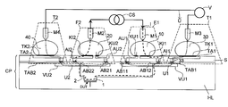
- FIG. 3A shows an embodiment example of a semiconductor arrangement with the measurement of a resistance.
- the semiconductor arrangement comprises the arrangement F 2 , depicted in FIG. 1 , another arrangement F 1 , a first and a second test apparatus T 1 and T 2 , and a current source CS to make available the measurement current I and a measuring device V to measure a voltage U.
- the arrangement F 1 corresponds in its structure and its function to the arrangement F 2 of FIG. 1 , but is depicted as a vertical reflection.
- the arrangement F 1 thus implements a first terminal 10 on which a test probe M 1 is placed.
- the arrangement F 1 moreover comprises a two-part contact area KI 1 , KU 1 , a two-part terminal surface AI 1 , AU 1 , and a two-part terminal area AB 11 , AB 12 .
- the different layers are connected among one another as depicted for the arrangement F 2 in FIG. 1 .
- the first test apparatus T 1 comprises a test probe M 3 , a first test terminal 30 , a first test contact area TK 1 , a first test terminal surface TA 1 , and a first test terminal area TAB 1 .
- the first test terminal area TAB 1 is connected with the first test terminal surface TA 1 in an electrically conductive manner via a through-connection 33 .
- the first test terminal surface TA 1 is connected with the first test terminal 30 , constructed as a solder ball, in an electrically conductive manner via the first test contact area TK 1 .
- the second test apparatus T 2 is constructed just like the first test apparatus T 1 . It comprises a test probe M 4 , a second test terminal 40 , a second test contact area TK 2 , a second test terminal surface TA 2 , and a second test terminal area TAB 2 .
- the semiconductor body CP has a first voltage connection VU 1 , a second voltage connection VU 2 , and an electronic component DUT to be tested in the semiconductor layer HL.
- the first voltage connection VU 1 connects the first part of the first terminal area AB 11 with the first test terminal area TAB 1 .
- the second voltage connection VU 2 connects the first part of the second terminal area AB 21 with the second test terminal area TAB 2 .
- the electronic component DUT to be tested is constructed as a transistor by way of example.
- a first terminal 1 of the component DUT is connected with the second part of the first terminal area AB 12 .
- a second terminal 2 of the component DUT is connected with the second part of the second terminal area AB 22 .
- the measurement current I is impressed at the first terminal 10 at the test probe M 1 .
- a closed circuit depicted with a broken line, is formed via the larger area of the first contact area KI 1 , the second part of the first terminal surface AI 1 , the second part of the first terminal area AB 12 , via the first terminal 1 of the electronic component DUT to the second terminal 2 of the electronic component DUT, and continues on via the second part of the second terminal area AB 22 to the second part of the second terminal surface AI 2 , to the larger area of the second contact area KI 2 , to the second terminal 20 .
- a first voltage path U 1 and a second voltage path U 2 are formed, which are depicted with dotted lines.
- the first voltage path U 1 leads from the underside of the first terminal 10 via the smaller area of the first contact area KU 1 , via the first part of the first terminal surface AU 1 , via the first part of the first terminal AB 11 , via the voltage connection VU 1 , to the first test terminal area TAB 1 , and continues on via the first test terminal surface TA 1 to the first test contact area TK 1 , and thus to the first test terminal 30 .
- the second voltage path U 2 leads from the underside of the second terminal 20 via the first part of the second contact area KU 2 , via the first part of the second terminal surface AU 2 , via the first part of the second terminal area AB 21 , via the second voltage connection VU 2 , to the second test terminal area TAB 2 , and continues on to the second test terminal surface TA 2 , to the second test contact area TK 2 , and thus to the second test terminal 40 .
- the voltage U is measured with the test probes M 3 and M 4 at the first test terminal 30 and at the second test terminal 40 .
- a resistance of the electronic component DUT is determined as a quotient of the voltage U and the measurement current I.
- the first terminal 10 and the second terminal 20 are each contacted with only one test probe. Nevertheless, this is a real four-wire measurement, and the resistance of the electronic component DUT can be determined directly.
- test terminals 30 and 40 can be placed at various measurement points to measure the resistances of other components via analogous multiplexers.
- the test terminals 30 and 40 need not be exclusively reserved for the testing, but rather can take over other functions in the normal operation of the integrated circuit implemented in the semiconductor body CP.
- FIG. 3B shows an embodiment example of a semiconductor arrangement with sequential measurement of a resistance.
- the depicted arrangement corresponds in its structure to the arrangement depicted in FIG. 3A , with changed voltage connections.
- the semiconductor layer HL also has a multiplexer component MUX.
- a first input E 1 of the multiplexer component MUX is connected with the first part of the first terminal area AB 11 .
- a second input E 2 of the multiplexer component MUX is connected with the first part of the second terminal area AB 21 .
- An output A of the multiplexer element MUX is connected with the first test terminal area TAB 1 via a voltage connection VU 12 .
- the measurement current I is again impressed at the first terminal 10 via the test probe M 1 .
- a closed current circuit is formed from the first terminal 10 , via the electronic component DUT, to the second terminal 20 .
- the measurement current I flows via the test probe M 2 back to the current source
- a constant reference potential is applied to the second test terminal 40 .
- a first partial voltage UT 1 is first read off between the first test terminal 30 and the second test terminal 40 . This corresponds to a voltage between the first input E 1 of the multiplexer component MUX and the second test terminal 40 . Subsequently, using the multiplexer component MUX, a second partial voltage UT 2 is read off with the test probes M 3 and M 4 .
- the partial voltage UT 2 drops between the second input E 2 of the multiplexer component MUX, that is, the second terminal 20 , and the second test terminal 40 .
- the voltage U between the first and the second terminals 10 and 20 is calculated as the difference between the two partial voltages UT 1 and UT 2 .
- FIG. 4 shows an embodiment example of a semiconductor arrangement without a cover layer S, in a side view.
- the semiconductor body CP here comprises only the semiconductor layer HL.
- a redistribution, or repositioning, of the terminals is not required in this arrangement. Consequently, the smaller area KU 2 of the second contact area is directly connected with the first part of the second terminal area AB 21 ; the larger area of the second contact area KI 2 is directly connected with the second part of the second terminal area AB 22 .
- the impressed measurement current I flows, via the larger area KI 2 of the second contact area directly to the second part of the second terminal area AB 22 .
- the second voltage path U 2 is formed from the underside of the second terminal 20 , via the smaller area KU 2 of the second contact area, to the first part of the second terminal area AB 21 .
- FIG. 5 shows the semiconductor arrangement of FIG. 4 in a top view.
- the terminal 20 formed as a solder ball and the test probe M 2 are not depicted here.
- the first part of the second terminal surface AB 21 and the second part of the terminal surface AB 22 are depicted on the semiconductor body HL.
- the smaller area KU 2 of the second contact area can be seen on the first part of the second terminal surface AB 21 .
- the larger area KI 2 of the second contact area can be seen on the second part of the second terminal area AB 22 .
- the contact areas KI 2 and KU 2 are formed as described for FIG. 2 , and are insulated from one another.
- FIG. 6 shows an embodiment example of a semiconductor arrangement without a cover layer S, with the measurement of a resistance.
- the semiconductor arrangement comprises the arrangement F 3 depicted in FIG. 4 , another arrangement F 4 , a third and a fourth test apparatus T 3 and T 4 , the current source CS to make available the measurement current I and the measuring device V to measure the voltage U corresponding to FIG. 3A .
- the arrangement F 4 corresponds, in its structure and in its function, to the arrangement F 3 depicted in FIG. 4 , but is depicted as a vertical reflection.
- the arrangement F 4 thus implements the first terminal 10 , on which the test probe M 1 is set.
- the arrangement F 3 implements the second terminal 20 .
- the third test apparatus T 3 comprises the test probe M 3 , the first test terminal 30 , the first test contact area TK 1 , and the first test terminal area TAB 1 .
- the first test contact area TK 1 is directly connected with the first test terminal area TAB 1 .
- the fourth test apparatus T 4 is constructed analogously to the third test apparatus T 3 and comprises the test probe M 4 , the second test terminal 40 , the second test contact area TK 2 , and the second test terminal area TAB 2 .
- the second test contact area TK 2 is directly connected with the second test terminal area TAB 2 .
- the impressing of the measurement current I at the test probe M 1 brings about a current flow from the first terminal 10 , via the larger area KI 1 of the first contact area, the second part of the first terminal area AB 12 , via the component DUT to be tested, to the second part of the second terminal area AB 22 , to the larger area KI 2 of the second contact area, to the second terminal 20 and to the test probe M 2 .
- the first voltage path U 1 and the second voltage path U 2 are formed. Analogously to the depiction for FIG.
- the first voltage path U 1 runs from the underside of the first terminal 10 via the smaller area KU 1 of the first contact area, via the first part of the first terminal area AB 11 , via the first voltage connection VU 1 , to the first test terminal area TAB 1 , and continues on via the first test contact area TK 1 , the first test terminal 30 , and the test probe M 3 to the voltage measuring device.
- the second voltage path U 2 runs from the underside of the second terminal 20 via the smaller area KU 2 of the second terminal area AB 21 , via the second voltage connection VU 2 , to the second test terminal area TAB 2 , and continues on via the second test contact area TK 2 , the second test terminal 40 , and the test probe M 4 to the voltage measuring device.
- the determination of the resistance is carried out as described for FIG. 3A .
- all contact resistances are recorded with the resistance measurement, in particular, the contact resistances between the two-part terminal areas AB 11 , AB 12 , and AB 21 , AB 22 , on the wafer and the respective solder ball of the first and second terminals 10 and 20 .
Landscapes
- Engineering & Computer Science (AREA)
- Physics & Mathematics (AREA)
- General Physics & Mathematics (AREA)
- Microelectronics & Electronic Packaging (AREA)
- Computer Hardware Design (AREA)
- Manufacturing & Machinery (AREA)
- General Engineering & Computer Science (AREA)
- Automation & Control Theory (AREA)
- Power Engineering (AREA)
- Testing Or Measuring Of Semiconductors Or The Like (AREA)
- Semiconductor Integrated Circuits (AREA)
Applications Claiming Priority (3)
| Application Number | Priority Date | Filing Date | Title |
|---|---|---|---|
| DE102008014774 | 2008-03-18 | ||
| DE102008014774.5 | 2008-03-18 | ||
| DE102008014774.5A DE102008014774B4 (de) | 2008-03-18 | 2008-03-18 | Halbleiteranordnung mit Testanschlüssen und Verfahren zur Messung eines Widerstandes zwischen zwei Anschlüssen eines Wafer-Level-Packages |
Publications (2)
| Publication Number | Publication Date |
|---|---|
| US20090237105A1 US20090237105A1 (en) | 2009-09-24 |
| US7948258B2 true US7948258B2 (en) | 2011-05-24 |
Family
ID=40580671
Family Applications (1)
| Application Number | Title | Priority Date | Filing Date |
|---|---|---|---|
| US12/406,721 Expired - Fee Related US7948258B2 (en) | 2008-03-18 | 2009-03-18 | Semiconductor arrangement and method for the measurement of a resistance |
Country Status (3)
| Country | Link |
|---|---|
| US (1) | US7948258B2 (de) |
| DE (1) | DE102008014774B4 (de) |
| GB (1) | GB2460310B (de) |
Families Citing this family (2)
| Publication number | Priority date | Publication date | Assignee | Title |
|---|---|---|---|---|
| KR101765656B1 (ko) * | 2010-12-23 | 2017-08-08 | 삼성디스플레이 주식회사 | 구동 집적회로 및 이를 포함하는 표시장치 |
| JP5819096B2 (ja) * | 2011-04-28 | 2015-11-18 | 富士通コンポーネント株式会社 | 接触端子装置 |
Citations (7)
| Publication number | Priority date | Publication date | Assignee | Title |
|---|---|---|---|---|
| JPH04373145A (ja) | 1991-06-24 | 1992-12-25 | Matsushita Electric Ind Co Ltd | 半導体装置とそれを用いた評価回路および評価方法 |
| US5760600A (en) * | 1995-08-28 | 1998-06-02 | Nec Corporation | Test device for insulated-gate field effect transistor and testing circuit and testing method using the same |
| US6018462A (en) | 1997-06-30 | 2000-01-25 | Nec Corporation | Multi-tip module |
| US6700399B1 (en) * | 2002-12-12 | 2004-03-02 | Texas Instruments Incorporated | High density parasitic measurement structure |
| US6853078B2 (en) | 2002-02-22 | 2005-02-08 | Matsushita Electric Industrial Co., Ltd. | Semiconductor device and method for fabricating the same |
| DE102004005586B3 (de) | 2004-02-04 | 2005-09-29 | Infineon Technologies Ag | Halbleiterbauteil mit einem Halbleiterchipstapel auf einer Umverdrahtungsplatte und Herstellung desselben |
| WO2006058019A1 (en) | 2004-11-22 | 2006-06-01 | Texas Instruments Incorporated | Method for capacitance measurement in silicon |
-
2008
- 2008-03-18 DE DE102008014774.5A patent/DE102008014774B4/de not_active Expired - Fee Related
-
2009
- 2009-03-05 GB GB0903787A patent/GB2460310B/en not_active Expired - Fee Related
- 2009-03-18 US US12/406,721 patent/US7948258B2/en not_active Expired - Fee Related
Patent Citations (8)
| Publication number | Priority date | Publication date | Assignee | Title |
|---|---|---|---|---|
| JPH04373145A (ja) | 1991-06-24 | 1992-12-25 | Matsushita Electric Ind Co Ltd | 半導体装置とそれを用いた評価回路および評価方法 |
| US5760600A (en) * | 1995-08-28 | 1998-06-02 | Nec Corporation | Test device for insulated-gate field effect transistor and testing circuit and testing method using the same |
| US6018462A (en) | 1997-06-30 | 2000-01-25 | Nec Corporation | Multi-tip module |
| US6853078B2 (en) | 2002-02-22 | 2005-02-08 | Matsushita Electric Industrial Co., Ltd. | Semiconductor device and method for fabricating the same |
| US6700399B1 (en) * | 2002-12-12 | 2004-03-02 | Texas Instruments Incorporated | High density parasitic measurement structure |
| DE102004005586B3 (de) | 2004-02-04 | 2005-09-29 | Infineon Technologies Ag | Halbleiterbauteil mit einem Halbleiterchipstapel auf einer Umverdrahtungsplatte und Herstellung desselben |
| US7521809B2 (en) * | 2004-02-04 | 2009-04-21 | Infineon Technologies Ag | Semiconductor device having a chip stack on a rewiring plate |
| WO2006058019A1 (en) | 2004-11-22 | 2006-06-01 | Texas Instruments Incorporated | Method for capacitance measurement in silicon |
Also Published As
| Publication number | Publication date |
|---|---|
| DE102008014774A1 (de) | 2009-09-24 |
| GB0903787D0 (en) | 2009-04-15 |
| GB2460310A (en) | 2009-12-02 |
| GB2460310B (en) | 2010-05-05 |
| US20090237105A1 (en) | 2009-09-24 |
| DE102008014774B4 (de) | 2015-09-03 |
Similar Documents
| Publication | Publication Date | Title |
|---|---|---|
| JP5486866B2 (ja) | 半導体装置の製造方法 | |
| US7105856B1 (en) | Test key having a chain circuit and a kelvin structure | |
| JP3794942B2 (ja) | マルチチップモジュール及びその接続テスト方法 | |
| JPH1070160A (ja) | 集積回路の電気的導通テストのための内蔵機能 | |
| KR20060108519A (ko) | 반도체 집적 회로 및 반도체 집적 회로 사이의 접속 상태의검사 방법 | |
| JP6765125B2 (ja) | 抵抗測定装置、基板検査装置、及び抵抗測定方法 | |
| US20190033365A1 (en) | Die crack detector and method therefor | |
| JP5529611B2 (ja) | 半導体装置及び抵抗測定方法 | |
| US7948258B2 (en) | Semiconductor arrangement and method for the measurement of a resistance | |
| TWI585426B (zh) | 電子裝置之基板及包含其之電子裝置 | |
| TW201538983A (zh) | 基板檢查裝置 | |
| JP2018166171A (ja) | 半導体装置の製造方法、半導体装置および半導体装置の検査装置 | |
| US6774649B2 (en) | Test system for conducting a function test of a semiconductor element on a wafer, and operating method | |
| JP2014143236A (ja) | 半導体装置 | |
| US7263759B2 (en) | Methods of manufacturing and testing bonding wires | |
| US10199292B2 (en) | Semiconductor device, semiconductor chip, and test method for semiconductor chip | |
| US20080211512A1 (en) | Test circuit arrangement and testing method for testing of a circuit section | |
| JP3395304B2 (ja) | 半導体集積回路の検査方法 | |
| US11428729B2 (en) | Device for testing a printed circuit board | |
| TW201728909A (zh) | 半導體裝置及其製造方法 | |
| Lim et al. | Methodology to determine high precision variation in the electrical resistance of copper wires due to corrosion | |
| JP3495835B2 (ja) | 半導体集積回路装置及びその検査方法 | |
| Seungje et al. | Detection of solder bump marginal contact resistance degradation using 4-point resistance measurement method | |
| JP7392533B2 (ja) | 検査システム | |
| US12094789B2 (en) | Analog sense points for measuring circuit die |
Legal Events
| Date | Code | Title | Description |
|---|---|---|---|
| AS | Assignment |
Owner name: AUSTRIAMICROSYSTEMS AG, AUSTRIA Free format text: ASSIGNMENT OF ASSIGNORS INTEREST;ASSIGNOR:COSTA, ALEXANDER;REEL/FRAME:022792/0922 Effective date: 20090422 |
|
| STCF | Information on status: patent grant |
Free format text: PATENTED CASE |
|
| FPAY | Fee payment |
Year of fee payment: 4 |
|
| MAFP | Maintenance fee payment |
Free format text: PAYMENT OF MAINTENANCE FEE, 8TH YEAR, LARGE ENTITY (ORIGINAL EVENT CODE: M1552); ENTITY STATUS OF PATENT OWNER: LARGE ENTITY Year of fee payment: 8 |
|
| FEPP | Fee payment procedure |
Free format text: MAINTENANCE FEE REMINDER MAILED (ORIGINAL EVENT CODE: REM.); ENTITY STATUS OF PATENT OWNER: LARGE ENTITY |
|
| LAPS | Lapse for failure to pay maintenance fees |
Free format text: PATENT EXPIRED FOR FAILURE TO PAY MAINTENANCE FEES (ORIGINAL EVENT CODE: EXP.); ENTITY STATUS OF PATENT OWNER: LARGE ENTITY |
|
| STCH | Information on status: patent discontinuation |
Free format text: PATENT EXPIRED DUE TO NONPAYMENT OF MAINTENANCE FEES UNDER 37 CFR 1.362 |
|
| FP | Lapsed due to failure to pay maintenance fee |
Effective date: 20230524 |