US7791108B2 - Nanowire tunneling transistor - Google Patents
Nanowire tunneling transistor Download PDFInfo
- Publication number
- US7791108B2 US7791108B2 US12/161,574 US16157407A US7791108B2 US 7791108 B2 US7791108 B2 US 7791108B2 US 16157407 A US16157407 A US 16157407A US 7791108 B2 US7791108 B2 US 7791108B2
- Authority
- US
- United States
- Prior art keywords
- nanowire
- transistor
- barrier
- transistor according
- drain
- Prior art date
- Legal status (The legal status is an assumption and is not a legal conclusion. Google has not performed a legal analysis and makes no representation as to the accuracy of the status listed.)
- Expired - Fee Related, expires
Links
Images




Classifications
-
- H—ELECTRICITY
- H10—SEMICONDUCTOR DEVICES; ELECTRIC SOLID-STATE DEVICES NOT OTHERWISE PROVIDED FOR
- H10D—INORGANIC ELECTRIC SEMICONDUCTOR DEVICES
- H10D30/00—Field-effect transistors [FET]
- H10D30/60—Insulated-gate field-effect transistors [IGFET]
- H10D30/751—Insulated-gate field-effect transistors [IGFET] having composition variations in the channel regions
-
- H—ELECTRICITY
- H10—SEMICONDUCTOR DEVICES; ELECTRIC SOLID-STATE DEVICES NOT OTHERWISE PROVIDED FOR
- H10D—INORGANIC ELECTRIC SEMICONDUCTOR DEVICES
- H10D62/00—Semiconductor bodies, or regions thereof, of devices having potential barriers
- H10D62/10—Shapes, relative sizes or dispositions of the regions of the semiconductor bodies; Shapes of the semiconductor bodies
- H10D62/117—Shapes of semiconductor bodies
- H10D62/118—Nanostructure semiconductor bodies
-
- B—PERFORMING OPERATIONS; TRANSPORTING
- B82—NANOTECHNOLOGY
- B82Y—SPECIFIC USES OR APPLICATIONS OF NANOSTRUCTURES; MEASUREMENT OR ANALYSIS OF NANOSTRUCTURES; MANUFACTURE OR TREATMENT OF NANOSTRUCTURES
- B82Y10/00—Nanotechnology for information processing, storage or transmission, e.g. quantum computing or single electron logic
-
- H—ELECTRICITY
- H10—SEMICONDUCTOR DEVICES; ELECTRIC SOLID-STATE DEVICES NOT OTHERWISE PROVIDED FOR
- H10D—INORGANIC ELECTRIC SEMICONDUCTOR DEVICES
- H10D30/00—Field-effect transistors [FET]
- H10D30/01—Manufacture or treatment
- H10D30/021—Manufacture or treatment of FETs having insulated gates [IGFET]
- H10D30/025—Manufacture or treatment of FETs having insulated gates [IGFET] of vertical IGFETs
-
- H—ELECTRICITY
- H10—SEMICONDUCTOR DEVICES; ELECTRIC SOLID-STATE DEVICES NOT OTHERWISE PROVIDED FOR
- H10D—INORGANIC ELECTRIC SEMICONDUCTOR DEVICES
- H10D30/00—Field-effect transistors [FET]
- H10D30/60—Insulated-gate field-effect transistors [IGFET]
- H10D30/63—Vertical IGFETs
-
- H—ELECTRICITY
- H10—SEMICONDUCTOR DEVICES; ELECTRIC SOLID-STATE DEVICES NOT OTHERWISE PROVIDED FOR
- H10D—INORGANIC ELECTRIC SEMICONDUCTOR DEVICES
- H10D62/00—Semiconductor bodies, or regions thereof, of devices having potential barriers
- H10D62/10—Shapes, relative sizes or dispositions of the regions of the semiconductor bodies; Shapes of the semiconductor bodies
- H10D62/117—Shapes of semiconductor bodies
- H10D62/118—Nanostructure semiconductor bodies
- H10D62/119—Nanowire, nanosheet or nanotube semiconductor bodies
- H10D62/121—Nanowire, nanosheet or nanotube semiconductor bodies oriented parallel to substrates
-
- H—ELECTRICITY
- H10—SEMICONDUCTOR DEVICES; ELECTRIC SOLID-STATE DEVICES NOT OTHERWISE PROVIDED FOR
- H10D—INORGANIC ELECTRIC SEMICONDUCTOR DEVICES
- H10D62/00—Semiconductor bodies, or regions thereof, of devices having potential barriers
- H10D62/10—Shapes, relative sizes or dispositions of the regions of the semiconductor bodies; Shapes of the semiconductor bodies
- H10D62/117—Shapes of semiconductor bodies
- H10D62/118—Nanostructure semiconductor bodies
- H10D62/119—Nanowire, nanosheet or nanotube semiconductor bodies
- H10D62/122—Nanowire, nanosheet or nanotube semiconductor bodies oriented at angles to substrates, e.g. perpendicular to substrates
-
- H—ELECTRICITY
- H10—SEMICONDUCTOR DEVICES; ELECTRIC SOLID-STATE DEVICES NOT OTHERWISE PROVIDED FOR
- H10D—INORGANIC ELECTRIC SEMICONDUCTOR DEVICES
- H10D62/00—Semiconductor bodies, or regions thereof, of devices having potential barriers
- H10D62/10—Shapes, relative sizes or dispositions of the regions of the semiconductor bodies; Shapes of the semiconductor bodies
- H10D62/117—Shapes of semiconductor bodies
- H10D62/118—Nanostructure semiconductor bodies
- H10D62/119—Nanowire, nanosheet or nanotube semiconductor bodies
- H10D62/123—Nanowire, nanosheet or nanotube semiconductor bodies comprising junctions
-
- Y—GENERAL TAGGING OF NEW TECHNOLOGICAL DEVELOPMENTS; GENERAL TAGGING OF CROSS-SECTIONAL TECHNOLOGIES SPANNING OVER SEVERAL SECTIONS OF THE IPC; TECHNICAL SUBJECTS COVERED BY FORMER USPC CROSS-REFERENCE ART COLLECTIONS [XRACs] AND DIGESTS
- Y10—TECHNICAL SUBJECTS COVERED BY FORMER USPC
- Y10S—TECHNICAL SUBJECTS COVERED BY FORMER USPC CROSS-REFERENCE ART COLLECTIONS [XRACs] AND DIGESTS
- Y10S977/00—Nanotechnology
- Y10S977/70—Nanostructure
- Y10S977/734—Fullerenes, i.e. graphene-based structures, such as nanohorns, nanococoons, nanoscrolls or fullerene-like structures, e.g. WS2 or MoS2 chalcogenide nanotubes, planar C3N4, etc.
- Y10S977/742—Carbon nanotubes, CNTs
- Y10S977/75—Single-walled
-
- Y—GENERAL TAGGING OF NEW TECHNOLOGICAL DEVELOPMENTS; GENERAL TAGGING OF CROSS-SECTIONAL TECHNOLOGIES SPANNING OVER SEVERAL SECTIONS OF THE IPC; TECHNICAL SUBJECTS COVERED BY FORMER USPC CROSS-REFERENCE ART COLLECTIONS [XRACs] AND DIGESTS
- Y10—TECHNICAL SUBJECTS COVERED BY FORMER USPC
- Y10S—TECHNICAL SUBJECTS COVERED BY FORMER USPC CROSS-REFERENCE ART COLLECTIONS [XRACs] AND DIGESTS
- Y10S977/00—Nanotechnology
- Y10S977/70—Nanostructure
- Y10S977/813—Of specified inorganic semiconductor composition, e.g. periodic table group IV-VI compositions
-
- Y—GENERAL TAGGING OF NEW TECHNOLOGICAL DEVELOPMENTS; GENERAL TAGGING OF CROSS-SECTIONAL TECHNOLOGIES SPANNING OVER SEVERAL SECTIONS OF THE IPC; TECHNICAL SUBJECTS COVERED BY FORMER USPC CROSS-REFERENCE ART COLLECTIONS [XRACs] AND DIGESTS
- Y10—TECHNICAL SUBJECTS COVERED BY FORMER USPC
- Y10S—TECHNICAL SUBJECTS COVERED BY FORMER USPC CROSS-REFERENCE ART COLLECTIONS [XRACs] AND DIGESTS
- Y10S977/00—Nanotechnology
- Y10S977/902—Specified use of nanostructure
- Y10S977/932—Specified use of nanostructure for electronic or optoelectronic application
- Y10S977/936—Specified use of nanostructure for electronic or optoelectronic application in a transistor or 3-terminal device
- Y10S977/938—Field effect transistors, FETS, with nanowire- or nanotube-channel region
Definitions
- the present invention is related to a nanowire tunneling transistor and in particular to a nanowire tunneling transistor according to claim 1 .
- MOSFET metal oxides semiconductor field effect transistors
- VLS vapor-liquid-solid
- a LOHN structure comprises at least one segment of a substantially crystalline material adjacent to at least another segment of a compositionally different material where a junction is formed there between.
- a LOHN structure is not limited to only two adjacent segments but can include a plurality of compositionally different materials. By the term “compositionally different” the following possibilities are encompassed:
- the nanowire heterostructure could comprise compositionally different materials when viewed longitudinally such as would be the case with alternating or periodic segments of different materials or multi segmented nanowires where at least two of the segments comprise different materials.
- a lateral MOSFET device concept that depends less on doping concentration and on channel length has been proposed in 1992 and has been described by R. Hattori, A. Nakae and J. Shirafuji in Jpn. J. Appl. Phys., vol. 31, p. L1467, 1992.
- This device used metal source and drain regions.
- the Schottky barriers between these regions can be modulated by a gate voltage applied to a gate electrode.
- the invention suggests a transistor comprising a nanowire having a source and a drain separated by an intrinsic or lowly doped region.
- a potential barrier is formed at the interface of the intrinsic or lowly doped region and one of the source and the drain.
- a gate electrode is provided in the vicinity of the potential barrier such that the effective height and/or width of the potential barrier can be modulated by applying an appropriate voltage to the gate electrode.
- a barrier region is located inside the intrinsic or lowly doped region between the source and the drain.
- the barrier region can be a highly doped semiconductor material.
- the material of the barrier region must be chosen such that it forms a narrow barrier to the adjacent lowly doped or intrinsic semiconductor regions. Examples of such a material are various metals and highly doped semiconductor regions with an appropriate electron affinity to ensure proper operation of the transistor.
- the semiconductor material forming the barrier region is indium arsenide while the adjacent intrinsic or lowly doped regions are made of silicon or gallium arsenide.
- the barrier is made from a metal.
- the potential barriers at the interfaces of the barrier region are usually referred to as Schottky barriers.
- the nanowire can be grown on a semiconductor substrate.
- the nanowire has highly doped end portions forming source and drain of the transistor.
- the outer surface of the nanowire is covered by an insulating layer.
- a metal layer is deposited forming a gate electrode.
- the insulating layer is a dielectric layer or a wide band gap semiconductor forming a Schottky barrier to the gate electrode.
- the wide band gap semiconductor forming the Schottky barrier to the gate electrode contains a delta-doped layer.
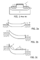
- FIG. 1 a schematic structure of a lateral Schottky source-drain MOSFET transistor which is known in the prior art
- FIGS. 2 a to 2 c show the electronic band structure of the transistor shown in FIG. 1 with different bias voltages applied;
- FIG. 3 a schematic of a known Schottky tunnel transistor
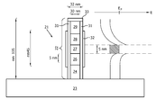
- FIG. 4 a schematic structure of a nanowire transistor according to a first embodiment of the present invention and its band structure
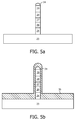
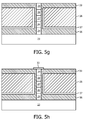
- FIGS. 5 a to 5 h a sequence of processing steps to fabricate the nanowire transistor structure of FIG. 4 ;
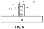
- FIG. 6 a schematic structure of a nanowire transistor according to a second embodiment of the present invention.
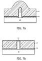
- FIGS. 7 a and 7 b a sequence of processing steps to fabricate the nanowire transistor structure of FIG. 6 .
- FIG. 1 shows a tunnel effect transistor as has been described by R. Hattori, A. Nakae and J. Shirafuji in Japanese Journal of Applied Physics, Volume 31 (1992), L1467 to L1469.
- the known transistor is a lateral transistor structure, which employs internal field emission of a Schottky barrier junction.
- the transistor which is designated as a whole with reference number 1 is fabricated on a conventional p-type silicon substrate 2 .
- a highly n-type doped channel layer 3 is realized on the topside of the substrate by conventional implantation of phosphorus or arsenic ions.
- the channel layer 3 is laterally defined by a masking step.
- a source 4 and a drain 6 are deposited by growing palladium silicide (PdSi) on top of the channel layer 3 .
- the source 4 and the drain 6 are separated by an insulator layer 7 made of silicon oxide (SiO 2 ) on top of which a metallic gate 8 is deposited.
- FIG. 2 a shows the band structure illustrated in FIG. 1 with no bias voltage applied between source 4 and drain 6 and with zero gate voltage.
- the Fermi level E F is a straight line across the whole band diagram of the transistor structure.
- the height of the Schottky barriers is indicated in FIG. 2 a as e ⁇ .
- FIG. 2 b shows the same band structure with a bias voltage applied between source 4 and drain 6 but with still no gate voltage applied.
- the Schottky barrier between source 4 and the channel 3 prevents electrons to flow from the source 4 to the drain 6 .
- FIG. 2 c shows the transistor 1 with an applied source-drain bias voltage and a positive gate voltage.
- the Schottky barrier between the source 4 and the channel 3 becomes thinner so that electrons e ⁇ can tunnel from the source 4 through the Schottky barrier and flow through the conduction band of the channel 3 into the drain 6 .
- the state shown in FIG. 2 c is designated as the ON state whereas the state shown in FIG. 2 b is designated as OFF state. In this way the current flow from the source 4 to the drain 6 is controlled by the gate voltage.
- FIG. 3 shows a Schottky tunnel transistor that has been described in IEEE Electron Device Letters, Vol. 15, No. 10, 1994, page 412.
- this tunnel transistor electrons can tunnel through a very thin Schottky barrier formed between an accumulation layer 17 and the gate 8 .
- this tunnel transistor contains only a single Schottky barrier.
- FIG. 4 shows a schematic structure of the transistor according to the invention in a cross sectional view.
- the transistor as a whole is designated with reference number 21 .
- the transistor 21 comprises a nanowire 22 , which is directly grown on a substrate 23 and which is realized as a longitudinal heterostructure.
- the present invention relates to nanowire structures with a diameter less than approximately 100 nm and preferably in the range of approximately 5 nm to approximately 50 nm with lengths in the range of approximately 50 nm to approximately 200 ⁇ m.
- Adjacent to the substrate 23 the nanowire 22 consists of highly n-type doped silicon forming the source 24 of the transistor 21 .
- the nanowire 22 continues with an intrinsic or lowly doped region 26 separating the source 24 from a barrier region 27 .
- the barrier region 27 is made from metallic material. In the present embodiment it is cobalt silicide (CoSi 2 ). But in other embodiments also other metallic materials or highly doped semiconductors with a small band gap like indium arsenide (InAs), which is compatible with the silicon nanowire 22 , could be used as well.
- the longitudinal nanowire 22 heterostructure continues again with a second intrinsic or lowly doped region 28 such that the barrier region 27 is sandwiched between the first and the second intrinsic or lowly doped regions 26 , 28 .
- the nanowire 22 is terminated with a highly n-type doped silicon region forming the drain 29 of the transistor 21 .
- the perimeter of the nanowire 22 is covered with an electrically insulating dielectric layer 31 .
- On the outer surface of the dielectric layer 31 a metallic gate layer 32 is deposited.
- the gate layer 32 is made e.g. from aluminum. However, aluminum is only one example and other metallic layers could be used as well.
- Schottky barriers are formed between the barrier region 27 and the intrinsic or lowly doped layers 26 , 28 .
- the Schottky barriers prevent electrons from flowing from the source 24 to the drain 29 .
- the height of the Schottky barriers can be modulated by a gate voltage applied to the gate 32 .
- a source-drain bias voltage is applied and a gate voltage lowers the Schottky barriers than a current flows from the source 24 to the drain 29 .
- the electronic structure of the transistor 21 is schematically visualized. At the interfaces between the barrier region 27 and the intrinsic or lowly doped regions 26 , 28 the Schottky barriers are formed.
- the dielectric layer 31 is replaced by a wide band gap semiconductor layer, e.g. Al 1-x Ga x As, which forms a Schottky barrier at the interface of the gate electrode.
- the wide band gap semiconductor layer may or may not contain a delta-doped layer (not shown in FIG. 4 ). The delta-doped layer increases the charge carrier density inside the nanowire 22 without introducing additional impurities inside the nanowire.
- the current is composed of a thermionic emission current across the Schottky barriers and a tunneling current through the Schottky barriers.
- the total current depends exponentially on the effective height and width of the Schottky barrier that can be modulated by the gate voltage. In this way a transistor action can be achieved.
- the effective gate length is defined by the thickness of the barrier region and can therefore be very thin. Accordingly the gate capacitance can be made very small and the transistor is appropriate to operate at high frequencies.
- the length of the gate is not defined by conventional masking techniques but rather by the thickness of the barrier region 27 , which is grown epitaxially, the gate length of the transistor according to the present invention can be much shorter than compared with conventional transistor structures.
- barrier region 27 consists of a highly doped low band gap semiconductor (e.g. InAs) it is separated from the intrinsic or lowly doped region by a more general potential barrier.
- a highly doped low band gap semiconductor e.g. InAs
- the dimensions of the transistor structure 21 can be taken from FIG. 4 as well.
- the total length of the transistor structure in a direction normal to the surface of the silicon substrate 23 is 105 nm.
- the diameter of the nanowire 22 is approximately 30 nm and its parameter is covered with the electrically insulating dielectric layer 31 having a thickness of 1 nm.
- the total diameter of the nanowire covered by the dielectric layer is consequently 32 nm.
- the length of the gate electrode 32 in the longitudinal direction of the nanowire is 45 nm while the thickness of the barrier region 27 in the longitudinal direction is only 5 nm.
- these dimensions are only presented as examples and should not be understood to limit the scope of the present invention.
- the intrinsic or lowly doped regions 26 , 28 are made of gallium arsenide (GaAs) instead of silicon (Si).
- the fabrication process begins with a standard n-type silicon substrate 23 which is made highly n-type doped by means of implantation.
- the doping level is in the order of 10 +19 cm ⁇ 3 and is achieved by implantation of arsenic (As) or phosphorus (P) ions.
- a commercially available implanter is used for this step.
- a catalyst region is defined containing a precursor metal layer that acts as a growth catalyst 34 .
- the catalyst 34 is used for the growth of a semiconducting nanowire. It is well known that a catalytic decomposition of a silicon containing gas by gold or iron can form long nanowires. This technique is usually called the vapor-liquid-solid (VLS) mechanism. A liquid nano droplet containing the metal and silicon is located at the tip of the growing wire.
- VLS vapor-liquid-solid
- gold and iron have a large diffusion coefficient in silicon and create deep electronic levels which are detrimental to the electronic performance of the finalized device. Therefore, metal silicides are much more preferred in semiconductor processing technologies when ever a metallic layer is necessary.
- nickel and cobalt silicides have been used but in the following the process based on cobalt is described for the sake of simplicity but without limiting the scope of the invention.
- a cobalt layer is deposited by chemical vapor deposition (CVD) on commercially available silicon substrates.
- CoCl 4 gas is introduced in a reactor in a H 2 ambience.
- the partial pressure of CoCl 4 is 0.06 Pascal and the total reactor pressure is 670 Pascal.
- the deposition temperature of the substrate is chosen to be in the range of 600 to 700° C. In a subsequent annealing step at elevated temperatures in the order of 900° C. the formation of cobalt silicide is terminated.
- the substrate is exposed to an atmosphere in the reactor of SiH 2 Cl 2 with a partial pressure of 70 Pascal in a 2.7 Kilopascal hydrogen atmosphere at temperatures around 650° C. Under these conditions silicon nanowires are growing on the cobalt silicide.
- the nanowire as a silicon/germanium heterostructure
- a laser is utilized to evaporate germanium in the furnace from a solid target.
- the laser beam heats up the surface of the germanium target placed inside the furnace until germanium atoms are evaporated.
- the evaporated germanium atoms are then incorporated into the nanowire.
- the nanowire as a axial Si/Ge heterostructure, i.e. the composition of the nanowire changes in its axial direction.
- One dimensional growth is maintained as long as the reacted decomposition takes place preferably at the interface between the cobalt silicide and the nanowire.
- the Ge atoms evaporated from the Ge target are also incorporated into the growing nanowire at the interface between the cobalt silicide and the nanowire.
- the silicon and germanium supplies alternatively on and off a nanowire is grown having a Si/Ge heterostructure in the axial direction of the nanowire.
- the nanowire becomes n-type doped by adding arsine (AsH 3 ) or phosphine (PH 3 ) to the incoming gas stream.
- the doping level is determined by the partial pressure of the arsine or phosphine gas.
- the barrier region 27 in this case is formed by highly n-doped Ge.
- the barrier region 27 consists of InAs or other small band gap semiconductors that can be grown as nanowires from the gaseous phase.
- heterostructure means in the present context a nanowire having a composition of different materials like silicon and germanium, the same material e.g. silicon having different doping types like n-type doped silicon and p-type doped silicon, and finally, the same material like silicon having different crystal orientations in the axial or radial direction of the nanowire.
- a radial heterostructure of a nanowire which is modulation doped e.g. of the surface of the nanowire can be very advantageous in the sense of a high majority carrier mobility.
- the structure is covered with a silicon oxide (SiO 2 ) layer 36 ( FIG. 5 b ).
- a metal layer 37 e.g. aluminum, is deposited on top of the SiO 2 layer 36 ( FIG. 5 c ).
- the metal layer 37 is covered by a thick highly n-doped polycrystalline silicon layer 38 with the exception of the top portion of the nanowire 22 ( FIG. 5 d ).
- the metal layer 37 is etched away where it is not covered by the polycrystalline silicon layer by means of an appropriate wet etch ( FIG. 5 e ).
- another SiO 2 layer 39 is deposited ( FIG. 5 f ).
- the ohmic contact 33 is made to the drain 29 .
- Contacts to the metal layer 38 forming the gate electrode are made in a conventional way by contacting the polycrystalline silicon layer.
- the source 24 is contacted by opening a window in the polycrystalline silicon and silicon oxide layers 38 , 39 and by making a contact to the highly n-doped substrate 23 .
- the polycrystalline silicon layer is replaced by a metallic layer.
- the silicon oxide forming the dielectric layer 36 can be replaced by other materials like wide band gap semiconductors forming a Schottky barrier at the interface to the gate electrode 38 .
- a delta-doped layer can be incorporated.
- FIG. 6 an alternative embodiment of the inventive transistor 21 ′ comprising a nanowire 22 ′ is illustrated. It does not include a barrier region and only one Schottky barrier is formed between the drain 29 and the intrinsic or lowly doped region 26 .
- the Schottky barrier between the drain and the intrinsic or lowly doped region 26 is modulated in a similar way as described for the transistor shown in FIG. 4 .
- the transistor 21 shown in FIG. 4 is symmetrical with respect to source 24 and drain 29 , i.e. exchanging the source and drain potentials only reverses the source-to-drain current but its magnitude remains the same. Contrary to that, the transistor 21 ′ is non-symmetrical because it contains only one Schottky diode.
- the nanowire 22 ′ is grown in a corresponding way to the nanowire 22 by the VLS growth process utilizing a growth catalyst 34 ( FIG. 7 a ).
- the main difference is that no barrier is grown in the nanowire 22 ′.
- the structure is covered with a dielectric layer 36 .
- a polycrystalline silicon layer 37 is deposited ( FIG. 7 a ).
- contacts are made to the source 24 , the drain 29 and the gate 32 ( FIG. 6 ).
- the dielectric layer 36 can be replaced by a wide band gap semiconductor material, which may be provided with a delta-doped layer as it has already been described above.
Landscapes
- Engineering & Computer Science (AREA)
- Chemical & Material Sciences (AREA)
- Nanotechnology (AREA)
- Physics & Mathematics (AREA)
- Mathematical Physics (AREA)
- Theoretical Computer Science (AREA)
- Crystallography & Structural Chemistry (AREA)
- Thin Film Transistor (AREA)
- Insulated Gate Type Field-Effect Transistor (AREA)
Applications Claiming Priority (6)
| Application Number | Priority Date | Filing Date | Title |
|---|---|---|---|
| EP06100816 | 2006-01-25 | ||
| EP06100816 | 2006-01-25 | ||
| EP06100816.5 | 2006-01-25 | ||
| IBPCT/IB2007/050241 | 2007-01-24 | ||
| PCT/IB2007/050241 WO2007086009A1 (en) | 2006-01-25 | 2007-01-24 | Nanowire tunneling transistor |
| WOPCT/IB2007/050241 | 2007-01-24 |
Publications (2)
| Publication Number | Publication Date |
|---|---|
| US20090008631A1 US20090008631A1 (en) | 2009-01-08 |
| US7791108B2 true US7791108B2 (en) | 2010-09-07 |
Family
ID=38007344
Family Applications (1)
| Application Number | Title | Priority Date | Filing Date |
|---|---|---|---|
| US12/161,574 Expired - Fee Related US7791108B2 (en) | 2006-01-25 | 2007-01-24 | Nanowire tunneling transistor |
Country Status (8)
| Country | Link |
|---|---|
| US (1) | US7791108B2 (de) |
| EP (1) | EP1979946B1 (de) |
| JP (1) | JP2009524924A (de) |
| KR (1) | KR20080096789A (de) |
| CN (1) | CN101375398B (de) |
| AT (1) | ATE529894T1 (de) |
| TW (1) | TW200739905A (de) |
| WO (1) | WO2007086009A1 (de) |
Cited By (9)
| Publication number | Priority date | Publication date | Assignee | Title |
|---|---|---|---|---|
| US20080093693A1 (en) * | 2006-10-20 | 2008-04-24 | Kamins Theodore I | Nanowire sensor with variant selectively interactive segments |
| US20120112157A1 (en) * | 2009-07-20 | 2012-05-10 | Quitoriano Nathaniel J | Nanowire sensor with angled segments that are differently functionalized |
| US8575624B2 (en) * | 2011-08-10 | 2013-11-05 | Kabushiki Kaisha Toshiba | Semiconductor device |
| US20130307513A1 (en) * | 2011-12-19 | 2013-11-21 | Han Wui Then | High voltage field effect transistors |
| US8975123B2 (en) | 2013-07-09 | 2015-03-10 | International Business Machines Corporation | Tunnel field-effect transistors with a gate-swing broken-gap heterostructure |
| US9978881B2 (en) | 2016-08-05 | 2018-05-22 | Samsung Electronics Co., Ltd. | Integrated circuit devices and method of manufacturing the same |
| US10483284B2 (en) | 2016-09-26 | 2019-11-19 | Korea University Research And Business Foundation | Logic semiconductor device |
| US10755937B2 (en) * | 2017-04-07 | 2020-08-25 | Semiconductor Manufacturing International (Shanghai) Corporation | Vertical transistor having a silicided bottom and method for fabricating thereof |
| US11342442B2 (en) | 2012-07-17 | 2022-05-24 | Unm Rainforest Innovations | Semiconductor product comprising a heteroepitaxial layer grown on a seed area of a nanostructured pedestal |
Families Citing this family (25)
| Publication number | Priority date | Publication date | Assignee | Title |
|---|---|---|---|---|
| EP1979935A1 (de) * | 2006-01-25 | 2008-10-15 | Nxp B.V. | Tunneltransistor mit barriere |
| WO2009072984A1 (en) * | 2007-12-07 | 2009-06-11 | Agency For Science, Technology And Research | A silicon-germanium nanowire structure and a method of forming the same |
| RU2367059C1 (ru) * | 2007-12-13 | 2009-09-10 | Институт радиотехники и электроники Российской Академии Наук | Туннельное устройство |
| EP2148374A1 (de) | 2008-07-23 | 2010-01-27 | University College Cork-National University of Ireland, Cork | Nanodraht-Tunneltransistor |
| US8114787B2 (en) * | 2009-02-19 | 2012-02-14 | Empire Technology Development Llc | Integrated circuit nanowires |
| KR20120003463A (ko) * | 2009-03-25 | 2012-01-10 | 글로 에이비 | 쇼트키 장치 |
| US9159565B2 (en) * | 2009-08-20 | 2015-10-13 | Globalfoundries Singapore Pte. Ltd. | Integrated circuit system with band to band tunneling and method of manufacture thereof |
| US20110087430A1 (en) | 2009-10-14 | 2011-04-14 | International Business Machines Corporation | Determining travel routes by using auction-based location preferences |
| TW201236154A (en) * | 2010-12-22 | 2012-09-01 | Ibm | Semiconductor device |
| US9368502B2 (en) * | 2011-10-17 | 2016-06-14 | GlogalFoundries, Inc. | Replacement gate multigate transistor for embedded DRAM |
| US9054215B2 (en) * | 2012-12-18 | 2015-06-09 | Intel Corporation | Patterning of vertical nanowire transistor channel and gate with directed self assembly |
| US8890119B2 (en) * | 2012-12-18 | 2014-11-18 | Intel Corporation | Vertical nanowire transistor with axially engineered semiconductor and gate metallization |
| US8896101B2 (en) * | 2012-12-21 | 2014-11-25 | Intel Corporation | Nonplanar III-N transistors with compositionally graded semiconductor channels |
| US9306063B2 (en) * | 2013-09-27 | 2016-04-05 | Intel Corporation | Vertical transistor devices for embedded memory and logic technologies |
| JP6146265B2 (ja) * | 2013-11-07 | 2017-06-14 | ソニー株式会社 | 顕微鏡システムおよびオートフォーカス方法 |
| US9318447B2 (en) | 2014-07-18 | 2016-04-19 | Taiwan Semiconductor Manufacturing Company Limited | Semiconductor device and method of forming vertical structure |
| TR201809995T4 (tr) * | 2014-09-24 | 2018-08-27 | Evonik Roehm Gmbh | Darbe mukavemeti olan iyileştirilmiş özellik profiline sahip kalıplama bileşiği. |
| US10121858B2 (en) * | 2015-10-30 | 2018-11-06 | Taiwan Semiconductor Manufacturing Company, Ltd. | Elongated semiconductor structure planarization |
| US11018254B2 (en) * | 2016-03-31 | 2021-05-25 | International Business Machines Corporation | Fabrication of vertical fin transistor with multiple threshold voltages |
| WO2017181404A1 (zh) | 2016-04-22 | 2017-10-26 | 华为技术有限公司 | 隧穿场效应晶体管及其制造方法 |
| WO2019046629A1 (en) | 2017-08-31 | 2019-03-07 | Micron Technology, Inc. | SEMICONDUCTOR DEVICES, HYBRID TRANSISTORS, AND ASSOCIATED METHODS |
| EP3676877A4 (de) * | 2017-08-31 | 2021-09-01 | Micron Technology, Inc. | Halbleiterbauelemente, transistoren und zugehörige verfahren zur kontaktierung von metalloxid-halbleiterbauelementen |
| CN109326650B (zh) * | 2018-10-10 | 2022-04-19 | 中国科学院微电子研究所 | 半导体器件及其制造方法及包括该器件的电子设备 |
| KR20220101861A (ko) * | 2021-01-12 | 2022-07-19 | 에스케이하이닉스 주식회사 | 수직형 트랜지스터 및 그 제조 방법 |
| CN112968053B (zh) * | 2021-02-01 | 2022-09-09 | 深圳大学 | 场效应晶体管及其制备方法 |
Citations (3)
| Publication number | Priority date | Publication date | Assignee | Title |
|---|---|---|---|---|
| WO2005124872A1 (en) | 2004-06-15 | 2005-12-29 | Koninklijke Philips Electronics N.V. | Nanowire semiconductor device |
| US7180107B2 (en) * | 2004-05-25 | 2007-02-20 | International Business Machines Corporation | Method of fabricating a tunneling nanotube field effect transistor |
| US20090224230A1 (en) * | 2006-06-09 | 2009-09-10 | Aaron Anthony Pesetski | Carbon nanotube field effect transistor |
Family Cites Families (2)
| Publication number | Priority date | Publication date | Assignee | Title |
|---|---|---|---|---|
| US7192533B2 (en) * | 2002-03-28 | 2007-03-20 | Koninklijke Philips Electronics N.V. | Method of manufacturing nanowires and electronic device |
| US7335908B2 (en) * | 2002-07-08 | 2008-02-26 | Qunano Ab | Nanostructures and methods for manufacturing the same |
-
2007
- 2007-01-24 CN CN2007800034256A patent/CN101375398B/zh not_active Expired - Fee Related
- 2007-01-24 WO PCT/IB2007/050241 patent/WO2007086009A1/en not_active Ceased
- 2007-01-24 EP EP07700680A patent/EP1979946B1/de active Active
- 2007-01-24 KR KR1020087020568A patent/KR20080096789A/ko not_active Ceased
- 2007-01-24 JP JP2008551929A patent/JP2009524924A/ja not_active Withdrawn
- 2007-01-24 AT AT07700680T patent/ATE529894T1/de not_active IP Right Cessation
- 2007-01-24 US US12/161,574 patent/US7791108B2/en not_active Expired - Fee Related
- 2007-01-25 TW TW096102854A patent/TW200739905A/zh unknown
Patent Citations (3)
| Publication number | Priority date | Publication date | Assignee | Title |
|---|---|---|---|---|
| US7180107B2 (en) * | 2004-05-25 | 2007-02-20 | International Business Machines Corporation | Method of fabricating a tunneling nanotube field effect transistor |
| WO2005124872A1 (en) | 2004-06-15 | 2005-12-29 | Koninklijke Philips Electronics N.V. | Nanowire semiconductor device |
| US20090224230A1 (en) * | 2006-06-09 | 2009-09-10 | Aaron Anthony Pesetski | Carbon nanotube field effect transistor |
Non-Patent Citations (7)
| Title |
|---|
| Hattori R et al; "A New Type of Tunnel-Effect Transistor Employing Internal Field Emission of Schottky Barrier Junction", Japanese Journal of Applied Physics, Tokyo, Japan. vol. 31, Part 2, No. 10B, Oct. 15, 1992, pp. L1467-L1469. |
| Kimura M et al; "A New Type of Schottky Tunnel Transistor", IEEE Electron Device Letters, vol. 15, No. 10, IEEE, IEEE Electron Devices Society, Piscataway, NJ. Oct. 1994, p. 412. |
| Lee C; "Single-Electron Tunnelling Transistor in SIGE/SI Double-Barrier Structures", Semiconductor Science and Technology, IOP, Bristol, GB. vol. 13, No. 8A, Aug. 1998, pp. A115-A118. |
| Ramgopal Rao V et al; "Simulation, Fabrication and Characterization of High Performance Planar-Doped-Barrier Sub 100 NM Channel Mosfets", Electron Devices Meeting, 1997. Technical Digest., International Washington, D.C., USA. Dec. 7-10, 1997, New York, NY, USA, IEEE, US, Dec. 7, 1997, pp. 811-814. |
| Rao V R et al; "Low Temperature-High Pressure Grown Thin Gate Dielectrics for MOS Applications", Microelectronic Engineering, Elsevier Publishers BV, Amsterdamn, NL, vol. 48, No. 1-4, Sep. 1999, pp. 223-226. |
| Sang-Mo Koo et al; "Silicon Nanowires as Enhancement-Mode Schottky Barrier Field-Effect Transistors", Nanotechnology, IOP, Bristol, GB, vol. 16, No. 9, Sep. 1, 2005, pp. 1482-1485. |
| Zhao Q et al; "Nanopatterning of Epitaxial COSI2 Using Oxidation in a Local Stress Field and Fabrication of Nanometer Metal-Oxide-Semiconductor Field-Effect Transistors", Journal of Applied Physics, American Institute of Physics, New York, US, vol. 96, No. 10, Nov. 15, 2004, pp. 5775-5780. |
Cited By (21)
| Publication number | Priority date | Publication date | Assignee | Title |
|---|---|---|---|---|
| US20080093693A1 (en) * | 2006-10-20 | 2008-04-24 | Kamins Theodore I | Nanowire sensor with variant selectively interactive segments |
| US20120112157A1 (en) * | 2009-07-20 | 2012-05-10 | Quitoriano Nathaniel J | Nanowire sensor with angled segments that are differently functionalized |
| US8569900B2 (en) * | 2009-07-20 | 2013-10-29 | Hewlett-Packard Development Company, L.P. | Nanowire sensor with angled segments that are differently functionalized |
| US8575624B2 (en) * | 2011-08-10 | 2013-11-05 | Kabushiki Kaisha Toshiba | Semiconductor device |
| US9685508B2 (en) | 2011-12-19 | 2017-06-20 | Intel Corporation | High voltage field effect transistors |
| US20130307513A1 (en) * | 2011-12-19 | 2013-11-21 | Han Wui Then | High voltage field effect transistors |
| US10263074B2 (en) | 2011-12-19 | 2019-04-16 | Intel Corporation | High voltage field effect transistors |
| US9245989B2 (en) * | 2011-12-19 | 2016-01-26 | Intel Corporation | High voltage field effect transistors |
| US11342442B2 (en) | 2012-07-17 | 2022-05-24 | Unm Rainforest Innovations | Semiconductor product comprising a heteroepitaxial layer grown on a seed area of a nanostructured pedestal |
| US11342438B1 (en) | 2012-07-17 | 2022-05-24 | Unm Rainforest Innovations | Device with heteroepitaxial structure made using a growth mask |
| US11342441B2 (en) | 2012-07-17 | 2022-05-24 | Unm Rainforest Innovations | Method of forming a seed area and growing a heteroepitaxial layer on the seed area |
| US11349011B2 (en) | 2012-07-17 | 2022-05-31 | Unm Rainforest Innovations | Method of making heteroepitaxial structures and device formed by the method |
| US11374106B2 (en) | 2012-07-17 | 2022-06-28 | Unm Rainforest Innovations | Method of making heteroepitaxial structures and device formed by the method |
| US11456370B2 (en) | 2012-07-17 | 2022-09-27 | Unm Rainforest Innovations | Semiconductor product comprising a heteroepitaxial layer grown on a seed area of a nanostructured pedestal |
| US9087717B2 (en) | 2013-07-09 | 2015-07-21 | International Business Machines Corporation | Tunnel field-effect transistors with a gate-swing broken-gap heterostructure |
| US8975123B2 (en) | 2013-07-09 | 2015-03-10 | International Business Machines Corporation | Tunnel field-effect transistors with a gate-swing broken-gap heterostructure |
| US9978881B2 (en) | 2016-08-05 | 2018-05-22 | Samsung Electronics Co., Ltd. | Integrated circuit devices and method of manufacturing the same |
| US10361319B2 (en) | 2016-08-05 | 2019-07-23 | Samsung Electronics Co., Ltd. | Integrated circuit devices |
| US10483284B2 (en) | 2016-09-26 | 2019-11-19 | Korea University Research And Business Foundation | Logic semiconductor device |
| US10755937B2 (en) * | 2017-04-07 | 2020-08-25 | Semiconductor Manufacturing International (Shanghai) Corporation | Vertical transistor having a silicided bottom and method for fabricating thereof |
| US10971367B2 (en) | 2017-04-07 | 2021-04-06 | Semiconductor Manufacturing International (Shanghai) Corporation | Method for fabricating vertical transistor having a silicided bottom |
Also Published As
| Publication number | Publication date |
|---|---|
| EP1979946A1 (de) | 2008-10-15 |
| WO2007086009A1 (en) | 2007-08-02 |
| ATE529894T1 (de) | 2011-11-15 |
| CN101375398A (zh) | 2009-02-25 |
| EP1979946B1 (de) | 2011-10-19 |
| CN101375398B (zh) | 2011-12-28 |
| KR20080096789A (ko) | 2008-11-03 |
| TW200739905A (en) | 2007-10-16 |
| US20090008631A1 (en) | 2009-01-08 |
| JP2009524924A (ja) | 2009-07-02 |
Similar Documents
| Publication | Publication Date | Title |
|---|---|---|
| EP1979946B1 (de) | Nanodraht-tunneltransistor | |
| US8134142B2 (en) | Tunneling transistor with barrier | |
| US7795677B2 (en) | Nanowire field-effect transistors | |
| US5923046A (en) | Quantum dot memory cell | |
| US8441043B2 (en) | Maskless process for suspending and thinning nanowires | |
| US7999251B2 (en) | Nanowire MOSFET with doped epitaxial contacts for source and drain | |
| JP5312938B2 (ja) | 電界効果トランジスタ | |
| US9318583B2 (en) | Tunnel field effect transistor and method for making thereof | |
| JP2011198938A (ja) | トランジスタ | |
| US10096711B2 (en) | Silicon-containing, tunneling field-effect transistor including III-N source | |
| KR100434534B1 (ko) | 쇼트키 터널 장벽을 이용한 단일 전자 트랜지스터 및 그 제조방법 | |
| US20250098515A1 (en) | Method of forming semiconductor device having carbon nanotube | |
| US7709923B2 (en) | Metal-base nanowire transistor | |
| JP7795234B2 (ja) | 電界効果トランジスタおよびスイッチ素子 |
Legal Events
| Date | Code | Title | Description |
|---|---|---|---|
| AS | Assignment |
Owner name: NXP, B.V., NETHERLANDS Free format text: ASSIGNMENT OF ASSIGNORS INTEREST;ASSIGNORS:HURKX, GODEFRIDUS ADRIANUS MARIA;AGARWAL, PRABHAT;REEL/FRAME:021265/0871 Effective date: 20070911 |
|
| REMI | Maintenance fee reminder mailed | ||
| LAPS | Lapse for failure to pay maintenance fees | ||
| STCH | Information on status: patent discontinuation |
Free format text: PATENT EXPIRED DUE TO NONPAYMENT OF MAINTENANCE FEES UNDER 37 CFR 1.362 |
|
| STCH | Information on status: patent discontinuation |
Free format text: PATENT EXPIRED DUE TO NONPAYMENT OF MAINTENANCE FEES UNDER 37 CFR 1.362 |
|
| FP | Lapsed due to failure to pay maintenance fee |
Effective date: 20140907 |
|
| AS | Assignment |
Owner name: MORGAN STANLEY SENIOR FUNDING, INC., MARYLAND Free format text: SECURITY AGREEMENT SUPPLEMENT;ASSIGNOR:NXP B.V.;REEL/FRAME:038017/0058 Effective date: 20160218 |
|
| AS | Assignment |
Owner name: MORGAN STANLEY SENIOR FUNDING, INC., MARYLAND Free format text: CORRECTIVE ASSIGNMENT TO CORRECT THE REMOVE APPLICATION 12092129 PREVIOUSLY RECORDED ON REEL 038017 FRAME 0058. ASSIGNOR(S) HEREBY CONFIRMS THE SECURITY AGREEMENT SUPPLEMENT;ASSIGNOR:NXP B.V.;REEL/FRAME:039361/0212 Effective date: 20160218 |
|
| AS | Assignment |
Owner name: MORGAN STANLEY SENIOR FUNDING, INC., MARYLAND Free format text: CORRECTIVE ASSIGNMENT TO CORRECT THE REMOVE APPLICATION 12681366 PREVIOUSLY RECORDED ON REEL 039361 FRAME 0212. ASSIGNOR(S) HEREBY CONFIRMS THE SECURITY AGREEMENT SUPPLEMENT;ASSIGNOR:NXP B.V.;REEL/FRAME:042762/0145 Effective date: 20160218 Owner name: MORGAN STANLEY SENIOR FUNDING, INC., MARYLAND Free format text: CORRECTIVE ASSIGNMENT TO CORRECT THE REMOVE APPLICATION 12681366 PREVIOUSLY RECORDED ON REEL 038017 FRAME 0058. ASSIGNOR(S) HEREBY CONFIRMS THE SECURITY AGREEMENT SUPPLEMENT;ASSIGNOR:NXP B.V.;REEL/FRAME:042985/0001 Effective date: 20160218 |
|
| AS | Assignment |
Owner name: NXP B.V., NETHERLANDS Free format text: RELEASE BY SECURED PARTY;ASSIGNOR:MORGAN STANLEY SENIOR FUNDING, INC.;REEL/FRAME:050745/0001 Effective date: 20190903 |
|
| AS | Assignment |
Owner name: MORGAN STANLEY SENIOR FUNDING, INC., MARYLAND Free format text: CORRECTIVE ASSIGNMENT TO CORRECT THE REMOVE APPLICATION 12298143 PREVIOUSLY RECORDED ON REEL 042762 FRAME 0145. ASSIGNOR(S) HEREBY CONFIRMS THE SECURITY AGREEMENT SUPPLEMENT;ASSIGNOR:NXP B.V.;REEL/FRAME:051145/0184 Effective date: 20160218 Owner name: MORGAN STANLEY SENIOR FUNDING, INC., MARYLAND Free format text: CORRECTIVE ASSIGNMENT TO CORRECT THE REMOVE APPLICATION 12298143 PREVIOUSLY RECORDED ON REEL 039361 FRAME 0212. ASSIGNOR(S) HEREBY CONFIRMS THE SECURITY AGREEMENT SUPPLEMENT;ASSIGNOR:NXP B.V.;REEL/FRAME:051029/0387 Effective date: 20160218 Owner name: MORGAN STANLEY SENIOR FUNDING, INC., MARYLAND Free format text: CORRECTIVE ASSIGNMENT TO CORRECT THE REMOVE APPLICATION 12298143 PREVIOUSLY RECORDED ON REEL 042985 FRAME 0001. ASSIGNOR(S) HEREBY CONFIRMS THE SECURITY AGREEMENT SUPPLEMENT;ASSIGNOR:NXP B.V.;REEL/FRAME:051029/0001 Effective date: 20160218 Owner name: MORGAN STANLEY SENIOR FUNDING, INC., MARYLAND Free format text: CORRECTIVE ASSIGNMENT TO CORRECT THE REMOVE APPLICATION12298143 PREVIOUSLY RECORDED ON REEL 039361 FRAME 0212. ASSIGNOR(S) HEREBY CONFIRMS THE SECURITY AGREEMENT SUPPLEMENT;ASSIGNOR:NXP B.V.;REEL/FRAME:051029/0387 Effective date: 20160218 Owner name: MORGAN STANLEY SENIOR FUNDING, INC., MARYLAND Free format text: CORRECTIVE ASSIGNMENT TO CORRECT THE REMOVE APPLICATION12298143 PREVIOUSLY RECORDED ON REEL 042985 FRAME 0001. ASSIGNOR(S) HEREBY CONFIRMS THE SECURITY AGREEMENT SUPPLEMENT;ASSIGNOR:NXP B.V.;REEL/FRAME:051029/0001 Effective date: 20160218 Owner name: MORGAN STANLEY SENIOR FUNDING, INC., MARYLAND Free format text: CORRECTIVE ASSIGNMENT TO CORRECT THE REMOVE APPLICATION 12298143 PREVIOUSLY RECORDED ON REEL 038017 FRAME 0058. ASSIGNOR(S) HEREBY CONFIRMS THE SECURITY AGREEMENT SUPPLEMENT;ASSIGNOR:NXP B.V.;REEL/FRAME:051030/0001 Effective date: 20160218 Owner name: MORGAN STANLEY SENIOR FUNDING, INC., MARYLAND Free format text: CORRECTIVE ASSIGNMENT TO CORRECT THE REMOVE APPLICATION12298143 PREVIOUSLY RECORDED ON REEL 042762 FRAME 0145. ASSIGNOR(S) HEREBY CONFIRMS THE SECURITY AGREEMENT SUPPLEMENT;ASSIGNOR:NXP B.V.;REEL/FRAME:051145/0184 Effective date: 20160218 |